


 View fulltext

2025
Volume: 42 Issue 4
20 Article(s)
Xuerong YE, Shanxue ZHAO, and Hao CHEN
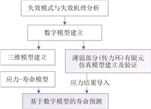
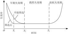
In response of the frequent failure problems of electromagnetic unlocking for aerospace separation electrical connectors,a reliability analysis method for the electromagnetic unlocking of separation electrical connectors is proposed based on digital models.A specific type of separation and release connector is selected as the research object.First,the functions,structure,and failure mechanisms of the connector are analyzed,by which the key failure modes are identified.Then,the digital models are used to simulate the unlocking process.A high-precision 3D model is established and combined with the finite element simulation analysis,by which the stresses exerted on the key components during the electromagnetic unlocking are analyzed.Finally,verification experiments are designed to validate the stress simulation results.Based on these results,the service life of the key components is predicted with the life prediction software.
Aug. 25, 2025Vol. 42 Issue 4 103 (2025)
Zhiwei ZHENG, Ranran ZHAO, Cen CHEN, Hao CHEN, and Guofu ZHAI
Highly reliable military microelectronic components are the cornerstone of quality in aerospace and defense weaponry.Design and manufacturing are the origins of reliability,while screening tests serve as a critical means to ensure it.Extensive screening,however,also increases the cost of component usage,making it urgently needed to carry out optimization research on screening tests oriented towards cost reduction.Currently,numerous studies have been conducted on the correlation between screening tests and manufacturing defects at home and abroad.The American Solid State Technology Association has even established the screening optimization standards for tailoring and optimizing later-stage screening tests by controlling the manufacturing defects.In this paper,the U.S.screening optimization standards are analyzed,and the manufacturing defects related to burn-in are examined.With the production testing data from 1 479 domestically produced 4-to-6-line decoders,the conditions required for optimizing burn-in test duration are determined.Additionally,the electrical parameters of both failed and normal devices under dynamic burn-in conditions are analyzed.The results reveal that,compared with the 240-h dynamic burn-in during the primary screening,the 40-h dynamic burn-in in the secondary screening induces a greater change in the input high-level current of the components.Furthermore,the 40-h dynamic burn-in in the secondary screening significantly reduces the static current,whereas the 240-h dynamic burn-in in the primary screening notably increases it.This indicates that the relationship between the burn-in duration and parameter drift is nonlinear,i.e.,longer burn-in time does not necessarily exert greater influence on the components.These findings demonstrate the feasibility of optimizing the duration of burn-in tests.
Aug. 25, 2025Vol. 42 Issue 4 112 (2025)
Yiwen LUO, Zhengdong SONG, Shaoxi ZHANG, Wei ZHANG, Haoran SUN, and Pengfei LIAN
To address the threats of radiation effects on the reliability in space environments,the radiation probabilistic risk assessment (PRA) methodologies for multi-core parallel fault-tolerant radiation-hardened computer systems (CCUs) are investigated.First,the single-event upset (SEU) rate distribution models for the critical memory devices,e.g.,programmable read only memory (PROM),magnetoresistive random access memory (MRAM),and static random access memory (SRAM),are developed based on the ground-based simulation test data.Three candidate empirical distributions,i.e.,exponential distribution,Weibull distribution,and log-normal distribution,are analyzed.The optimal fitting function is selected according to the maximum entropy principle,and it is shown that the SEU rates of the memory devices follow the log-normal distribution most reasonably.Second,a device failure probability model is established under the framework of the error detection and correction (EDAC) mechanisms.A system-level reliability modeling method is constructed for the CCUs,and the Monte Carlo simulation is adopted to derive the failure probability distribution over a 5-year mission lifecycle.Finally,the probability importance,structural importance,and relative importance of the components are analyzed,and the critical risk sources are quantified,by which the device hardening strategies and risk mitigation recommendations are suggested.The findings provide a theoretical foundation and quantitative support for the design of highly reliable radiation-tolerant systems.
Aug. 25, 2025Vol. 42 Issue 4 120 (2025)
Lindong MA, Zhengdong SONG, Yuan LIU, Bo WANG, and Zebin KONG
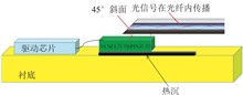
High-speed space communication networks urgently require optical modules featuring high bandwidth,low latency,and miniaturization.In this paper,the displacement damage effect,single-event effect (SEE),and temperature characteristics of optical modules are investigated,aiming to elucidate the degradation patterns and underlying mechanisms of the key parameters of the optical modules in the space environment.Through the environmental tests,it is found that the incident neutrons introduce displacement damage defects in the vertical-cavity surface-emitting laser (VCSEL) and positive-intrinsic-negative (PIN) detector of the optical module,reducing the minority carrier lifetime and thus decreasing the optical output power and receiver sensitivity.The optical module is susceptible to the SEE.The heavy ions cause bit-flips in the registers within the driver circuits,resulting in communication bit-errors and communication interruptions.The threshold current of the VCSEL increases with temperature,which is the main reason for the degradation in the optical output power of the transmitter module.
Aug. 25, 2025Vol. 42 Issue 4 129 (2025)
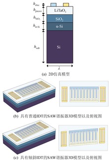
Shijia LI, Zonglin WU, Hangyu QIAN, and Guomin YANG
With the growing demand for 5G technology applications,there is an urgent need to improve the performance of surface acoustic wave (SAW) filters in radio frequency (RF) front-end modules.The shear horizontal (SH) SAW resonators based on piezoelectric thin films exhibit excellent characteristics.However,some transverse spurious modes may appear in the admittance responses of SAW resonators,leading to severe in-band ripples in the SAW filters constructed from such resonators,which hinders their application in 5G technology.This paper proposes an SH-SAW resonator based on a hetero-layered substrate of 42°Y-cut LiTaO?/SiO?/α-Si/Si.To investigate the generation of transverse modes,the dispersion characteristics and slowness curves of the device are analyzed using the finite element method (FEM).The fabricated SAW resonator with normal interdigital transducers (IDTs) achieves an electromechanical coupling coefficient (keff2) of 11.1% and a Bode-Qmax of 1 317.Additionally,an SAW resonator with tilted IDTs is fabricated to suppress the spurious modes.With a tilt angle of 6°,the measured results demonstrate effective suppression of transverse spurious modes.
Aug. 25, 2025Vol. 42 Issue 4 53 (2025)
Junya YANG, Liangping WANG, Yamei LIN, Yanlin LI, Wei SHI, and Jichao LIU
This paper focuses on the extreme environmental adaptability and high-performance requirements of aerospace antenna arrays.A domestically-produced low-temperature co-fired ceramic (LTCC) substrate material is selected to develop a low profile,lightweight,miniaturized,circularly-polarized,4×4 scale highly-reliable antenna array with a center frequency of 12 GHz.The structural design and testing results of the antenna array are analyzed,and the effects of material changes on the electrical performance of the antenna array under irradiation environments and the reliability of the antenna array structure under extreme temperature conditions are investigated by simulations.The results show that the parameter performance changes of domestically-produced LTCC materials have little influence on the electrical performance and structural reliability of the antenna array under irradiation and extreme temperature conditions.The relative impedance bandwidth (S11<-10 dB) of the antenna array is 41.6%,the 3 dB axial ratio relative bandwidth is 33.8%,and the maximum gain is 15 dBi.The antenna array has excellent performance and high structural reliability,and can be widely used in aerospace circularly-polarized communication systems.
Aug. 25, 2025Vol. 42 Issue 4 59 (2025)

Lin DU, Yan JIANG, Zebin KONG, Bo WANG, Minwei ZHU, Lanlai WANG, and Kunshu WANG
The evolution trend of advanced packaging architectures for microsystem devices is analyzed,and the reliability issues and risks of the most widely used 2.5D advanced packaging structure for microsystems are summarized.In view of the difficulties in detecting typical risks of high-value microsystem devices,the non-destructive testing methods are studied.The experiment adopts a 3D micro computed tomography (CT) method,and the characteristics of 2.5D advanced microsystem packaging are analyzed based on a nano-microfocus X-ray tube.For the first time,a contour analysis method based on 2D solder ball virtual slice data is proposed,and the analysis accuracy of the micro-warpage of the interposer reaches 1 μm.The 3D non-destructive testing accuracy of the fine size of the internal through silicon via (TSV) is verified by comparing the TSV 2D slice data with the scanning electron micro-scope sample data.The copper convex morphology in the interposer is confirmed by the analysis on the experimental data of the interposer.The measured data are displayed,which characterize the quality of the micro-solder joints of the resistor welding on the interposer.This paper provides a new evaluation method for the reliability evaluation of advanced microsystem packaging.The experimental data confirm the effectiveness of the method,and provide a reference for the defect identification.
Aug. 25, 2025Vol. 42 Issue 4 66 (2025)
Wuying MA, Lili DING, Jifang LI, Chen PAN, and Liangliang MIN
To elucidate the physical mechanisms underlying the synergistic effects between the total γ dose and neutron displacement damage in bipolar process devices,in this paper,the experiments of neutron irradiation followed by γ-ray exposure and γ-ray exposure followed by neutron irradiation are conducted with the Xi’an pulsed reactor and the irradiation facility of 60Co,taking the bipolar circuits,transistors,and diodes as the experimental subjects.The experimental results demonstrate that,for bipolar process circuits,the damage induced by the neutron irradiation followed by γ-ray exposure is more severe than that caused by the γ-ray exposure followed by neutron irradiation.Tests with diodes and gate-controlled transistors are also carried out,which demonstrates that the interaction between the defects generated by the neutron/γ synergistic effects,or between the radiation and pre-existing defects,is relatively weak.This is mainly because the neutron irradiation facilitates the migration of hydrogen from the passivation layer into the oxide layer,which subsequently accelerates the generation of interface trap charges during the total dose irradiation.These findings provide significant insights for the radiation-hardened design of bipolar devices and the assessment of their performance in mixed radiation fields.
Aug. 25, 2025Vol. 42 Issue 4 75 (2025)
Xing LI, Teng MA, Silei ZHONG, Chao PENG, Hong ZHANG, Zhangang ZHANG, and Zhifeng LEI
The single-event burnout (SEB) phenomenon in β-Ga2O3 Schottky barrier diode (SBD) under heavy ion and high-energy proton irradiation conditions is systematically investigated.The results demonstrate that the reverse bias voltage is a crucial factor influencing the failure of β-Ga2O3 SBDs.SEB occurs only when the reverse bias voltage reaches a specific critical value,and the higher the reverse bias voltage,the shorter the time to failure.Through the technology computer aided design (TCAD) simulations and scanning electron microscopy (SEM) analysis,the mechanisms behind SEB are further elucidated,showing that the accumulation of high electric fields and the electron-hole pairs induced by the irradiation are the primary causes of SEB.The thermal effects and enhanced electric field induced by high-energy proton and heavy ion irradiation lead to localized overheating in the device,which in turn triggers the occurrence of SEB.This research provides theoretical insights and engineering references for optimizing the design of β-Ga2O3 devices and improving their radiation hardness,which is crucial for applications in high-radiation environments.
Aug. 25, 2025Vol. 42 Issue 4 81 (2025)
Zitao ZHAO, Lin WEN, Yudong LI, Jie FENG, Bingkai LIU, and Qi GUO
High-energy protons in space can cause performance degradation and pixel anomalies in complementary metal oxide semiconductor (CMOS) image sensors (CISs),significantly affecting space object detection.To gain a deeper understanding of the random telegraph signal (RTS) pixel issues induced by high-energy protons in CISs,in this paper,some proton irradiation tests are carried out on space-grade CISs,combined with several room-temperature and high-temperature annealing tests.The generation patterns of the RTS pixels are obtained,and the mechanisms underlying the RTS pixel formation are analyzed.The results show that the dark signals of the RTS pixels caused by protons can fluctuate across up to nine levels.The higher the number of levels,the fewer the number of RTS pixels,but the more frequent the transitions of the dark signals between levels become.This study suggests that the fluctuations in RTS pixel dark signals originate from the variations in defect configurations,with phosphorus-vacancy (VP) defects playing a significant role in the formation of RTS pixels.The findings provide a basis for the radiation hardening and on-orbit maintenance of CISs.
Aug. 25, 2025Vol. 42 Issue 4 89 (2025)
Xiaofan ZHAO, Zhongfang WANG, Maodan Ma, Tao ZHANG, Hongyu DING, Yanguang LI, and Yongheng YANG
This article focuses on the ionizing total dose effects of the analog integrated circuits in space radiation environments and the corresponding hardening strategies based on the standard bipolar process.The irreplaceable core role of analog circuits in spacecraft is discussed,the physical mechanisms of the ionizing total dose effects and their degeneration mechanisms on bipolar circuits are analyzed,and the necessity of hardening design is emphasized.The circuit hardening methods are elaborated in detail.Taking the operational amplifiers and voltage reference as examples,the degradation mechanisms of the total ionizing dose effects and the key points of the hardening design are specifically analyzed.The results show that,without designed hardening,the operational amplifiers based on the standard bipolar process will experience serious parameter deviations under the total ionizing dose of 30 krad(Si) (1 rad = 0.01 J/kg).Conducting circuit hardening design for sensitive parameters can enhance the space radiation tolerance of bipolar analog circuits,which is of great significance for ensuring the long-term reliable operation of spacecraft.
Aug. 25, 2025Vol. 42 Issue 4 97 (2025)
Linsheng WU, Yi HUANG, Liang ZHOU, Min TANG, Xiaochun LI, and Junfa MAO
With the development of electronic systems towards higher integration density and performance,conventional radio frequency (RF) integration technologies struggle to meet the demands,and the RF front-end microsystem technology based on three-dimensional (3D) heterogeneous integration has emerged as a critical breakthrough direction.This paper focuses on the application of the RF front-end microsystem technology in the aerospace field.The key scientific challenges requiring resolution are described,including the RF microsystem architecture,multi-physics coupling,and co-simulation design methodologies.Furthermore,the specific technological advancements in microsystem electronic design automation (EDA) tools,heterogeneous integration processes,and testing/verification methods are introduced.Additionally,the research achievements of the authors’ team in millimeter-wave band RF front-end microsystems are also presented.The RF front-end microsystem technology holds significant strategic importance for driving innovation in aerospace RF equipment,enhancing mission execution capabilities,and promoting civil-military integration.It serves as a core enabler for achieving high-performance,miniaturized RF devices in aerospace applications.
Aug. 25, 2025Vol. 42 Issue 4 1 (2025)
Yuan LI, Yue HAO, Yuanfu ZHAO, Xiaohua MA, Xuefeng ZHENG, Danning TANG, Weibo JIANG, Chenyang NIU, and Xinyue LI
The aerospace industry is at the forefront of significant technological advancements,as it adopts emerging solutions for power conversion based on ultra-wide bandgap semiconductor devices to meet the escalating demands for improved efficiency,reduced weight,and enhanced thermal performance in aerospace power electronics applications.On one hand,β-Ga2O3 has emerged as a promising candidate for high-efficiency,high-power-density power electronics applications,owing to its large bandgap and rapid development speed in semiconductor devices.On the other hand,the reliability evaluation and applications of β-Ga2O3 devices in extreme aerospace environments still face numerous unknowns and challenges.This paper thoroughly explores the pressing demand for ultra-wide bandgap semiconductor devices in aerospace power electronics,and offers an in-depth review of the global research progress on the radiation effects in gallium oxide power devices.It is believed that conducting comprehensive studies on radiation-induced defect targets and their associated signal transduction mechanisms within β-Ga2O3 material-device systems not only can advance a robust,closed-loop methodology for evaluating radiation reliability in ultra-wide bandgap compound semiconductors spanning from materials to devices,but also can establish a critical database linking radiation exposure conditions to quantitative device degradation metrics.Ultimately,this research provides pivotal insights for optimizing material growth,designing forward radiation-hardened power devices,and strengthening redundancy-based strategies for device-integrated power electronics systems.
Aug. 25, 2025Vol. 42 Issue 4 16 (2025)
Kunshu WANG, Ranran ZHAO, Rong ZHAO, Bo WANG, Zebin KONG, and Minwei ZHU
With the increasingly stringent requirements for the product cost control in aerospace engineering,the low-cost application approaches for aerospace components and their quality assurance mechanisms have become a critical research focus at present.This paper systematically reviews the research progress and practical experience regarding the low-cost component selection strategies and quality assurance methodologies at home and abroad.On this basis,the core challenges of achieving effective cost control while maintaining the inherent quality and reliability of the components for aerospace models are focused.The component cost structures and quality grades are analyzed in detail,and an integrated cost control scheme is proposed.The scheme centers on implementing a combined selection mechanism based on the mission-criticality classification of aerospace models and component-category management and differentially formulating the targeted screening test strategies according to the specific quality grades of the components.The proposed classification-based management framework and differentiated screening strategy recommendations aim to provide theoretical reference and practical guidance for aerospace model engineering to ensure the high-reliability application and assured quality of components under stringent cost constraints.
Aug. 25, 2025Vol. 42 Issue 4 28 (2025)
Yu HAN, Tao YING, Jianqun YANG, and Xingji LI
Owing to its radiation effects on the radiation-sensitive materials and devices as well as biological entities and crew members onboard spacecraft,the extreme and complex space radiation environment has been identified as a significant challenge threatening the long-term operational reliability of spacecraft and the success of space missions.To accurately analyze the influence of radiation effects on in-orbit spacecraft and implement necessary protective design measures,research teams from international organizations including the National Aeronautics and Space Administration (NASA),the European Space Agency (ESA),and Centre National d'études Spatiales (CNES) have conducted extensive investigations over recent decades,developing diverse simulation analysis methods and tools for space radiation effects.This paper comprehensively reviews the knowledge graph encompassing space radiation environments,various radiation effects,and the evolutionary development of domestic and international radiation effect simulation tools.The typical applications and critical roles of space radiation effect simulation technologies in space missions are summarized,while critically evaluating the limitations in existing radiation effect analysis methods and tools.Finally,the emerging trends and prioritized research directions for radiation effect simulation technologies in future space applications are proposed.
Aug. 25, 2025Vol. 42 Issue 4 39 (2025)
Xiuqing HAO, Simin CHEN, Lingchen MENG, Kewei FU, Liyuan XU, Huangcheng ZHU, Guoqiang GUO, and Ning HE
New materials and structures have been continuously developed and applied in the aerospace field,and their unique properties such as lightweight,high strength,and heterogeneous composites,along with increasingly complex and high-precision structural designs,have imposed stricter requirements on the efficient and precise machining of aerospace components.Laser processing has been widely applied in the aerospace manufacturing field,owing to its advantages of non-contact operation,high precision,and high efficiency.In this paper,the principles of laser processing,typical applications,and current research status at home and abroad are investigated from four perspectives,i.e.,laser cutting,laser welding,laser drilling,and laser surface processing.The application scopes,advantages,and disadvantages of laser processing are compared with other machining technologies in the aerospace field,and the future development directions are proposed.
Aug. 25, 2025Vol. 42 Issue 4 136 (2025)
Zhenqi YANG, Chang HE, Zhihang JING, and Jianjun LUO
To address the challenge of threat assessment for multi-space non-cooperative targets,a multi-space non-cooperative target threat assessment method based on the dynamic Bayesian network (DBN) and the technique for order preference by similarity to ideal solution (TOPSIS) is proposed.First,the key threat factors of spatial non-cooperative targets are analyzed and extracted from a mission-oriented perspective,and a DBN model is constructed to represent their dynamic interrelationships.Meanwhile,an intent recognition module is incorporated into the threat assessment framework to enhance the accuracy and rationality of threat level estimation for individual targets.Second,the TOPSIS method is adopted to quantify and rank the threat levels of multi-space non-cooperative targets.Finally,simulations and analyses are conducted for the target threat assessment under representative scenarios to validate the effectiveness and applicability of the proposed threat assessment approach.
Aug. 25, 2025Vol. 42 Issue 4 158 (2025)
Xiao LIU, Xiuwei LI, Xiaojia LIU, Cheng JIN, and Haibo HONG
The construction requirements for intelligent workshops in aerospace manufacturing under both internal and external environments are analyzed,and a model and data hybrid-driven architecture for the intelligent workshop management and control platform in aerospace manufacturing is proposed,along with the core content of its hierarchical structure.The industrial internet platform based on the middle-platform concept and microservice architecture is elaborated.The key technologies for the intelligent workshops in aerospace manufacturing are elaborated in detail,including the multi-source heterogeneous real-time data acquisition and storage technology,unified modeling technology for multi-dimensional and multi-scale workshop models,microservice decomposition and business integration technology for workshop management and control,and digital twin-based optimization control technology for workshop operations.Finally,the feasibility of the architecture is validated through three typical cases of intelligent workshop construction in aerospace enterprises.
Aug. 25, 2025Vol. 42 Issue 4 171 (2025)
Miao XIN, Yang RUAN, Yusong LI, and Shaoyi LI
Owing to the complex highlighted background interference in medium-wave images and low target signal-to-clutter ratio (SCR) in long-wave images,the performance of visual tasks in a single band is limited.In order to solve such problems,along with the consideration of the inherent difference and complementary information of the target and background in different band infrared images,a fusion algorithm of infrared dual-band images based on the visual state space model (VMamba) is proposed.First,the global perception ability of the VMamba module is used to establish the long-distance dependence between the target and the background,and the feature information of different band images is extracted and effectively integrated.Second,the semantic information of the target and background is combined to improve the algorithm's ability to perceive the salient features of the target.Finally,under the guidance of improving the performance of downstream tasks,a dual-band image fusion evaluation metric,i.e.,background residual (BR),is proposed to measure the suppression effect of the fused image on the background clutter.The test results in the infrared dual-band measured image data set constructed in this paper show that the proposed infrared dual-band fusion algorithm has the abilities of enhancing the target characteristics and suppressing the background clutter.An SCR of 0.636 and a BR of 2.846×10⁻³ are obtained.The SCR is 1.605% higher than that obtained from the optimal general algorithm curvelet transform (CVT),and the BR is 1.625% higher than that obtained from the optimal general algorithm,i.e.,multiscale singular value decomposition (MSVD).
Aug. 25, 2025Vol. 42 Issue 4 180 (2025)
Xuedong SONG, Di PAN, Sijia PAN, Da LIAN, Libin LI, and Weizhi QU
The optical detection products for space targets are an important part of satellite engineering, and their reliability and accuracy are crucial factors in determining the effectiveness of on-orbit missions. However, stray light can seriously affect the on-orbit performance of such products. Moreover, the existing anti-stray light algorithms usually have limited feature extraction and high false alarm rates, or complex processing and large computational load, and are not suitable for real-time on-orbit processing. In this paper, a stray light filtering algorithm for space object detection is proposed. The algorithm extracts three types of feature quantities based on independent image blocks, including grayscale mean, intra-block grayscale gradient, and maximum intra-block grayscale difference between classes. It determines the degree of stray light interference, takes the corresponding filtering measures, and finally filters out the effective image data containing the target. In addition, this algorithm can achieve parallel computing along with image data streams through hardware, with a simple calculation process and excellent real-time performance. It is convenient to be embedded in products as embedded modules. The results of simulation and outdoor star observation experiments indicate that the algorithm has exceedingly good performance in filtering stray light. It has stable and reliable target detection capabilities even under stray light interference, and has a low false alarm rate. The algorithm can significantly improve the anti-stray light ability and on-orbit reliability of space target detection products such as star sensors and wide-field space target surveillance cameras.
Aug. 25, 2025Vol. 42 Issue 4 189 (2025)
© Copyright 2018-2021 | Chinese Laser Press.
All Rights Reserved 沪ICP备15018463号-20