


Please enter the answer below before you can view the full text.


2024
Volume: 61 Issue 19
25 Article(s)

Bitao Shen, Huajin Chang, Haowen Shu, and Xingjun Wang
Integrated microcavity comb technology exploits optical nonlinearity within integrated microcavities to generate periodic optical pulses under continuous optical pumping. These pulses exhibit equidistant optical-frequency components in the frequency domain. Compared to traditional optical combs, integrated microcavity optical combs offer advantages such as miniaturization, low power consumption, and high repetition rates. Their unique time-frequency characteristics not only facilitate the evolution of traditional optical combs toward on-chip integration but also enable integration with wavelength division multiplexing technology to advance on-chip parallelization, high-capacity information transmission, processing, and sensing. In the generation of microcavity combs, the dispersion of microcavities—i.e., the difference in the group velocity of light at different wavelengths within the cavity—is crucial. Different application requirements necessitate specific cavity dispersion designs. This article reviews the research progress on how dispersion influences optical comb states, discusses recent advancements in integrated microcavity dispersion design, and summarizes current technologies and challenges while looking forward to future developments.
Oct. 10, 2024Vol. 61 Issue 19 1913001 (2024)
Hongwei Wang, Lu Sun, Yong Zhang, Luqi Yuan, Jianwen Dong, and Yikai Su
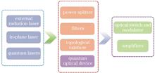
Topological photonics provides new ideas for optical information processing. Furthermore, research on the application of topological edge states to construct nanophotonic devices is developing rapidly. Additionally, topological waveguides have many unique advantages in designing on-chip integrated optoelectronic devices, such as high phase-shifting efficiency and many tunable degrees of freedom, which further inspire researchers to examine and explore them extensively. The research progress based on integrated topological photonic devices is introduced. First, several typical topological lasers based on different topological systems are summarized. Second, on-chip topological passive devices, such as topological power dividers, wavelength multiplexers and demultiplexers, topological rainbows and topological filters are introduced. Third, topological integrated active devices, including topology optical switches and topology modulators, which are important devices for optical signal processing, acquisition, and conversion, are highlighted. Finally, there are topologically integrated quantum optical devices that cover topological quantum light sources and devices in topological quantum information processing. However, certain challenges remain in the application of topological photonics in integrated optoelectronic devices, such as the high loss of topological waveguides and material compatibility, which are briefly discussed in this study. The research progress on on-chip integrated topological photonic devices is summarized and future directions are explored, providing new ideas for the development of integrated optoelectronic devices.
Oct. 10, 2024Vol. 61 Issue 19 1913002 (2024)
Qiang Li, Ruifeng Zhong, Zhaohui Li, and Jingshun Pan
We recently designed a novel on-chip photonic chip based on the chalcogenide glass material (ChG)-Ge26Sb10S64 (GeSbS) to satisfy the demands of optical information processing, optical sensing, and integrated system applications. Chalcogenide glass possesses unique advantages, such as a high photoelastic coefficient, a low transmission loss, an ultra-wide transparency window, and an easy on-chip hybrid integration process. These advantages confer significant benefits upon chalcogenide photonic integrated devices in terms of efficiency in optical sensing applications, thereby facilitating multifunctional integration and resulting in excellent sensing performance. This study combines the characteristics of chalcogenide materials to develop various ChG-based hybrid integrated chips and provides a review of their applications in ultrasonic signal detection, optoacoustic imaging, and acousto-optic modulation. Finally, this study discusses the challenges faced by chalcogenide photonic integrated devices and prospects for future research.
Oct. 10, 2024Vol. 61 Issue 19 1913003 (2024)
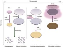
Xu Gao, and Lin Chang
Silicon photonics has emerged as a transformative technology for integrated photonics and has rapidly advanced over the past few decades. Heterogeneous integration facilitates the seamless integration of active and passive devices, including lasers and detectors, into silicon photonics systems. High-quality III-V semiconductor lasers on silicon platforms offer remarkable potential for creating cost-effective, high-density integrated light source for silicon photonics chips. This paper reviews the prevalent methods for heterogeneous integration and recent advancements in the integration of silicon and III-V semiconductor lasers, highlighting their optical applications across various chips. The development trends and future prospects of silicon-based integrated light sources are also analyzed and discussed.
Oct. 10, 2024Vol. 61 Issue 19 1913004 (2024)
Zheng Li, Mingfei Liu, and Chao Xiang
Photonic integrated circuits (PICs) are playing an increasingly important role in the fields of interconnection, sensing, and computing. Heterogeneously integrated lasers can improve the integration, portability and scalability of PICs, help them achieve more complex advanced functions, and achieve large-scale fabrication at the low-cost wafer level. Due to the cost and performance advantages demonstrated by heterogeneously integrated lasers, they have rapidly advanced in the fields of narrow linewidth lasers, tunable lasers, and comb lasers in recent years. They also play a crucial role in applications such as data center interconnection, sensing, microwave generation, and electronicphotonic heterogeneous integration. This paper firstly compares the schemes of different integrated lasers, then reviews the development history of heterogeneously integrated lasers, and summarizes the wide application scenarios of heterogeneously integrated lasers. Finally, the heterogeneously integrated lasers are summarized and prospected. Heterogeneously integrated lasers will further release the potential of PICs with their own advantages, breaking through the power consumption, cost and speed bottlenecks of PICs.
Oct. 10, 2024Vol. 61 Issue 19 1913005 (2024)
Minglu Cai, Jianping Chen, and Kan Wu
Erbium-doped lithium niobate thin films offer a promising optoelectronic platform by combining the gain performance with the electro-optic and nonlinear properties of lithium niobate, potentially enabling single-chip full integration. This study aims to develop an integrated waveguide amplifier based on erbium-doped lithium niobate thin films to meet the growing demand for compact and efficient optical amplifiers in optical communication networks. This study explores on-chip gain theory and conduct experimental validation. A lithium niobate waveguide with a propagation loss as low as 0.18 dB/cm was prepared by combining electron beam lithography with dry etching. Employing a 1484-nm bidirectional pumping scheme, a 10-cm-long integrated waveguide amplifier demonstrated a signal enhancement of 62.76 dB and a net gain of 22.26 dB. The experimental characterization results closely align with the gain simulation outcomes. This research provides a critical experimental basis and theoretical support for further optimizing integrated optical amplifiers based on erbium-doped lithium niobate thin films and broadening their applications in optical communication.
Oct. 10, 2024Vol. 61 Issue 19 1913006 (2024)
Ying Xue, and Lau Kei May
III-V active devices and their efficient coupling and integration with passive components are crucial for the further development of silicon photonics. Heteroepitaxy for integrating efficient III-V lasers on silicon can enable wafer-scale silicon photonic-integrated circuits, maximizing the benefits of silicon photonics at low cost, high throughput, large bandwidth, and large-scale integration. This article examines III-V active devices on silicon-on-insulator (SOI) via lateral selective epitaxy, focusing on the integration of III-V lasers and photodetectors on SOIs and their efficient in-plane coupling with silicon-based passive components. This article discusses their unique characteristics, including bufferless, in-plane configurations and laterally stacked active regions, as well as their future development prospects.
Oct. 10, 2024Vol. 61 Issue 19 1913007 (2024)
Yifei Zhang, Huashan Yang, Pavlov Nikolay, Jijun He, and Shilong Pan
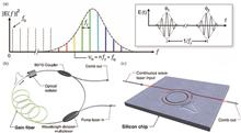
Dissipative Kerr solitons are broadband, low-noise optical-frequency combs generated using optical microresonators. They produce stable temporal pulses and demonstrate significant potential for use in spectral analysis, communications, and precision measurement. A breather soliton, which is a unique subset of dissipative Kerr solitons, is characterized by its rhythmic pulse-duration and peak-intensity oscillations. In this study, we scrutinized the dynamics of a breathing dissipative Kerr soliton within a silicon-nitride microresonator. We experimentally observed a breathing frequency of approximately 290 MHz, which shows instability in the megahertz range, thus posing a significant challenge to practical applications. Nevertheless, by applying an appropriate modulation signal to the pump laser within the fluctuation range of the breather's frequency, the breathing frequency can be injection locked to the frequency of the modulation signal, with the injection locking not exceeding 10 MHz, and the linewidth is compressed from 11 MHz to 35 kHz after locking. Additionally, we discovered another type of breather during our experiments, which was induced by intermodal interactions and had a breathing frequency of approximately 295 MHz. This breather was subjected to injection locking, which stabilized its frequency. Our study provides innovative avenues for the practical utilization of whispering gallery modes within microcavities, which are anticipated to be applied as multiwavelength sources in multichannel amplitude-modulated continuous-wave LiDAR technology.
Oct. 10, 2024Vol. 61 Issue 19 1913008 (2024)
Bigeng Chen, Ke Li, Yiru Zhao, and Shaoliang Yu
As one of the core devices in optical systems for interconnect, communication, and sensing, electro-optical modulators are in charge of the critical functionality of electric-optical signal conversion. Silicon electro-optical modulators based on silicon on insulator (SOI) exhibit various advantages such as compact size, high modulation efficiency, and CMOS fabrication compatibility. Therefore, they have been a hot topic for years and are being commercially deployed on a large scale. Furthermore, the popularization of artificial intelligence and rise of hyper data centers continuously drive the development and innovation of electro-optical modulators. This review first introduces the two principles of silicon electro-optical modulation—free carrier plasma dispersion effect and DC Kerr effect—followed by the common modulation mechanisms and classical forms of devices. Subsequently, we present recent typical innovative advances in high-speed optical interconnects, microwave photonics, and optical sensing. Finally, we summarize the development status and opportunities of silicon electro-optical modulators and discuss the existing challenges, emphasizing the importance of the original innovations of the modulation principle.
Oct. 10, 2024Vol. 61 Issue 19 1913009 (2024)
Yiwei Xie, Jiachen Wu, Xinyan Ju, Zezhong Zhou, Yujun Liu, Shengyao Qian, Shunhua Liu, Huan Li, and Daoxin Dai
Photonic signal processing, an important aspect of information systems, is also crucial in practical applications. Large-scale programmable photonic signal processors, owing to their high flexibility, low cost, and powerful processing capabilities, have become a focus of current research. In terms of implementation, silicon photonic technology offers advantages such as compactness, low power consumption, and compatibility with existing CMOS processes. Remarkable progress has been made in this technology over the past decade, leading to its emergence as a highly promising integrated platform. The integration of large-scale programmable photonic signal processors on silicon-based chips not only facilitates device miniaturization but also ensures system stability and high performance. In this study, we review the research progress of large-scale programmable silicon-based integrated chips in the fields of microwave photonics, optical communications, and photonic computing and discuss the challenges associated with the further development of such chips.
Oct. 10, 2024Vol. 61 Issue 19 1913010 (2024)
Rong Wang, Zhenzhou Tang, Dapeng Liu, Tian Cui, Naidi Cui, and Shilong Pan
This paper presents an active mode-locking optoelectronic oscillator (AML-OEO) utilizing a microring resonator. AML is achieved by integrating a Mach–Zehnder modulator (MZM) into a conventional OEO loop and varying the signal frequency applied to the MZM. Experimental results show that microwave frequency combs with repetition rates of 5.93, 29.65 MHz, and 59.3 MHz can be generated by fundamental, 5th-order harmonic, and 10th-order harmonic mode-locking, respectively. Compared to the phase noise of signals generated by a free-running OEO, that in the case of the AML-OEO at a center frequency of 14.64 GHz remains consistent across different orders of harmonic modes, with a phase noise of approximately -92 dBc/Hz@10 kHz.
Oct. 10, 2024Vol. 61 Issue 19 1913011 (2024)
Weixi Liu, Hengzhen Cao, Chengfeng Wen, Jiahao Wu, Yuanchen Chen, Daoxin Dai, and Yaocheng Shi
Traditional interferometric fiber optic gyroscopes (IFOGs) are constrained by performance bottlenecks inherent in separate system architectures, which severely impede further enhancements in navigation system capabilities. The integration of IFOG technology with optical engine chips offers a compelling solution to these bottlenecks. This paper reviews the integrated optical engine chip technology used in IFOG systems. The paper begins with an overview of the basic working principles of IFOGs, based on the Sagnac effect, and investigates the development of multifunctional integrated optical engine chips using various materials, including silicon, indium phosphide, silicon dioxide, and silicon nitride. Subsequently, the paper presents a comprehensive analysis of the current state of hybrid integrated optical engine chips, showcasing recent advances in system integration and functional diversity. Finally, the main challenges encountered in current research and application are analyzed, and the future development path of integrated optical engine chip technology in the IFOG field is discussed.
Oct. 10, 2024Vol. 61 Issue 19 1913012 (2024)
Ciyuan Qiu, Ning Ma, Yu Chen, and Yikai Su
Programmable silicon multifunction photonic chips are key components in the field of information photonics. They can be widely used in various important applications, including high-speed, multifunctional on-chip optical logic computing, and optical signal processing. In such chips, silicon-integrated devices are used to construct an on-chip optical network. Meanwhile, functional programming and signal loading of the device can be realized by loading the thermal and electrical signals on the optoelectronic device. In this way, multifunctional operations can be implemented using a single chip. Recently, domestic and foreign research teams have made important contributions in these areas. However, current programmable silicon multifunctional chips have several drawbacks, such as speed, integration density, and the automatic programming method. In this paper, we present the basic principle and performance of the demonstrated chips. We also discuss their applications and future prospects.
Oct. 10, 2024Vol. 61 Issue 19 1913013 (2024)
Zan Zhang, and Beiju Huang
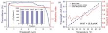
A spectrometer is one of the most important testing instruments that can directly reflect the spectral information of materials as it determines the existence and composition of substances. It is crucial in fields such as material characterization and analysis. Owing to the widespread application of spectral analysis technology in various fields, the limitations of conventional spectrometers have become increasingly apparent, particularly in terms of miniaturization, integration, and cost reduction. In recent years, the computational reconstruction spectrometer has garnered significant attention owing to its small size and low hardware cost. Silicon photonics technology, owing to its mature manufacturing processes, high integration, and excellent performance, provides a new approach to achieving miniaturized, low-cost chip-based computational reconstruction spectrometers. This article reviews the research progress of computational reconstruction spectrometers based on silicon photonics technology, with emphasis on their operating principles, key components, and spectral reconstruction algorithms. Silicon photonics technology provides researchers with various spectral sampling units and encompasses multimode waveguides, linear coherent networks, reconfigurable optical networks, programmable filters, etc. It offers the advantages of high integration, wide spectral range, and high resolution. Its miniaturization potential and new material applications expand its functions, thus rendering it suitable for environmental monitoring, food safety, and medical diagnosis, particularly in portable health monitoring. This review is anticipated to provide a comprehensive reference and inspiration for researchers in the field as well as offer guidance for the further research and application of silicon photonics technology.
Oct. 10, 2024Vol. 61 Issue 19 1913014 (2024)
Ziwei Zhou, Chengkun Dong, Jiayi Wang, Qing He, Yiyun He, and Jun Xia
Liquid crystal metasurfaces (LCMs) have emerged as a promising technique in optical device research due to their ability of flexibly and dynamically control electromagnetic wave properties such as amplitude, phase, polarization, and wavefront. This review discusses the progress in the design and application of LCMs, highlighting their significant potential in various fields like optical detection, imaging, and computation. LCM leverage the high degree of freedom in sub-wavelength structural design, enabling dynamic modulation of optical characteristics through external electric fields. The paper explores the principles behind LCMs, including the integration of liquid crystal materials with metasurfaces to achieve real-time optical property adjustments. Various applications such as tunable filters, beam steering, and dynamic holography are examined. Additionally, the review covers both contact and non-contact LCMs, outlining the mechanisms of phase modulation and information channel switching. The challenges and future prospects of LCMs in enhancing optical communication, sensing, and display technologies are also discussed, providing a comprehensive overview of this cutting-edge field.
Oct. 10, 2024Vol. 61 Issue 19 1913015 (2024)
Hao Li, Fengjun Li, and Xiangping Li
Optical neural networks, which use photons as information carriers and are used to construct optical neurons and optical synaptic connection models, are key components for achieving high-performance computing tasks in optical artificial intelligence. Metasurfaces, composed of subwavelength artificial nanostructures capable of multidimensional light field manipulation, have become a new platform for optical neural networks, offering new possibilities for parallel processing of large-scale intensive computational tasks. This article presents a review of the development and challenges of metasurface-based optical diffraction neural networks. First, it introduces the realization of optical field multitask parallel-processing approaches using metasurface optical diffraction neural networks, the preparation of chip integration, and their applications in image recognition and classification, optical information processing, and complex visual tasks. Finally, it concludes with an outlook on the challenges and future development of metasurface optical diffraction neural networks.
Oct. 10, 2024Vol. 61 Issue 19 1913016 (2024)
Guoyan Zeng, Yuexin Yin, Yingzhi Ding, Xiaoqiang Sun, and Daming Zhang
In this study, a variable optical attenuator for multi-band use based on silica platform is demonstrated. The device is based on the Mach-Zehnder interferometer (MZI) structure with two Bessel curve multi-mode interferometers (MMIs). The variable optical attenuators are prepared to operate in the O+E+S+C+L band (1260?1625 nm) and spectral range of 365 nm. The insertion loss is lower than 10.94 dB with an extinction ratio larger than 8.06 dB. The maximum power consumption of these states is lower than 452.1 mW. At the wavelength of 1310 nm, the rise and fall time of the optical signal are 0.84 ms and 0.88 ms, respectively. Meanwhile, at the wavelength of 1550 nm, the rise and fall time of the optical signal are 0.72 ms and 1.04 ms, respectively. The device has good application prospects in the field of optical communication.
Oct. 10, 2024Vol. 61 Issue 19 1913017 (2024)
Ziyuan Chang, Haoxuan Zhang, Biyan Zhan, Lin Song, and Xianwen Liu
Low half-wave-voltage electro-optic phase modulators can reduce system power consumption and simplify driving circuits, which are crucial in optical signal processing. Using X-cut thin-film lithium niobate photonic platforms and the principle of radio-frequency (RF) phase-delay modulation, we optimized the optical and electrical parameters of a cross-waveguide phase modulator with ground-signal-ground electrodes. Preliminary experiments were conducted to verify the modulator performance. At an in-phase modulation frequency of 17.5 GHz and a total modulation length of 10 mm, the RF voltage-length product was experimentally measured to be 7.5 V·cm, consistent with the design results. Increasing the total modulation length to 40 mm further reduced the half-wave voltage to 2.2 V. A passive waveguide transmission loss of approximately 0.4 dB/cm was measured from the co-integrated microring resonator. At a high RF driving power of 29 dBm, the operation of the cross-waveguide phase modulator in the high-frequency region of 30 GHz was verified. This research offers guidance for designing and analyzing on-chip electro-optic modulators with low half-wave voltages.
Oct. 10, 2024Vol. 61 Issue 19 1913018 (2024)
Bing Chang, Yiyang Gu, Xinyue He, Yupei Liang, Yaqian Zhao, Weixun Zhang, Feilong Dong, Bowen Li, Teng Tan, and Baicheng Yao
Optical frequency combs consist of a series of evenly spaced frequency components with stable phase interrelationships across the spectrum. Since their inception, they have brought about significant advancements in the fields of optical frequency metrology and precision measurement. With continuous innovation in micro-nano processing technology, researchers have successfully realized the generation of microcavity optical frequency combs based on the third-order Kerr effect on chip-scale platforms. These on-chip integrated Kerr optical frequency combs have the advantages of large channel spacing, exceptional coherence, small size, low power consumption, and easy integration. Additionally, they are compatible with complementary metal oxide semiconductor processes, enabling low-cost, large-scale fabrication and bringing significant opportunities for applications in microwave photonics, precision optical sensing, coherent communication with multiple sources, and other on-chip integrated systems. Currently, sensing applications based on on-chip integrated Kerr optical frequency combs are developing rapidly, with technical solutions continually being updated, bringing new breakthroughs in functionality and performance. Focusing on the engineering technology, first, this paper provides an overview of the emerging material platforms and recent research progress in the generation of on-chip integrated Kerr optical frequency combs. Second, it reviews advancements in their applications in optical sensing fields, such as lidar, precision spectroscopy, and distributed fiber sensing. Finally, it summarizes and provides an outlook on the current research status and future development prospects of on-chip integrated Kerr optical frequency combs.
Oct. 10, 2024Vol. 61 Issue 19 1913019 (2024)
Yifei Wang, Lifeng Chen, Zhongjin Lin, and Xinlun Cai
Optical coherence tomography (OCT) is a noninvasive high-resolution three-dimensional imaging technology that has been extensively used in medicine, thin-film material fabrication, and other fields. OCT is particularly applied in ophthalmic disease diagnosis and is widely recognized as the gold standard for cross-sectional retinal imaging in ophthalmology. However, the development of applications in the traditional OCT system is limited as it comprises discrete bulky optical components. Recently, the introduction of photonic integrated circuit (PIC) technology and integration of the traditional discrete components of OCT systems into optoelectronic chips have enabled OCT systems to come into a new phase that features smaller size, lower cost, and stronger stability. This review discusses the operating principle and key performance parameters of the OCT system, including the resolution, imaging speed, imaging depth, and signal-to-noise ratio. Additionally, it outlines the design methodology of PIC-based OCT. Furthermore, this review provides a comprehensive overview of recent advancements in OCT systems based on a PIC. It assesses the strengths and weaknesses of various material platforms for OCT system applications and analyzes potential challenges encountered by current research on PIC-based OCT systems. Finally, it presents a perspective on future development directions and potential research opportunities.
Oct. 10, 2024Vol. 61 Issue 19 1913020 (2024)
Tiantian Li, Yijie Li, Zihan Bai, Yumeng Liu, Dongdong Han, Zhanqiang Hui, and Huimin Du
Silicon photonic switches that use phase change materials offer solutions to the high power consumption and large size challenges faced by traditional optical switch technologies. However, the high absorption properties of conventional optical phase change materials impose limitations on the integration scale of optical switch arrays. Due to its reversible phase transitions between single-crystal states and low structural entropy, In2Se3 is promising for advancing high-speed, stable, and low-power optical switch technology. This study presents a non-volatile photonic switch based on In2Se3 and silicon waveguides that is composed of a directional coupler structure formed by multiple silicon waveguides and a single heterogeneously integrated Si-In2Se3 waveguide. Utilizing the non-volatile phase transition characteristics between α-In2Se3 and β-In2Se3, the device can switch the output between the cross and bar ports of the directional coupler, thus enabling a waveguide-type switch that does not require continuous power supply. Simulation results show that at 1550 nm, the optical switch achieves insertion losses of less than 0.86 dB at both the cross and bar ports, with a channel crosstalk of more than -20.39 dB. The proposed structure is expected to inspire technological developments in fields such as optical communications and photonic information processing.
Oct. 10, 2024Vol. 61 Issue 19 1913021 (2024)
Jinkui Chu, Jiaxin Fu, and Jianying Liu
In this study, we present the design of an integrated polarization optical sensor based on a dielectric metasurface. The sensor consists of a dielectric metasurface, double-layer field diaphragm, and complementary metal oxide semiconductor (CMOS) image sensor. We first design a dielectric metasurface to decompose incident light into six orthogonal polarized components. We next analyze the optical path structure of the sensor and fabricated a micro-nano-processed double-layer field diaphragm to eliminate ambient stray light. We then construct a sensor alignment platform and completed the preparation process for the sensor on this platform. Finally, we calibrate and test the sensor. Following calibration, the measurement error of the full Stokes parameter is ±0.15, and the polarization angle error is ±0.3°. The sensor has the advantages of being small in size and multi-directional as well as having the ability to measure all Stokes parameters.
Oct. 10, 2024Vol. 61 Issue 19 1913022 (2024)
Chenye Wei, Li Tian, Yingqi Feng, and Yongxin Zhu
This paper presents a design scheme of high-resolution digital LCoS chip, which can be used in the wavelength selective switch in all-optical communication networks. The LCoS chip-driving algorithm, overall architecture, component module simulation, and system verification results are presented. The pixel unit adopts the 9T static random-access memory (SRAM) scheme, which realizes two selectable modes of high-speed progressive refresh and global refresh on digital pixels for the first time. This design is based on 0.18 μm complementary metal-oxide-semiconductor transistor (CMOS) technology. Through optimization, the relatively small pixel size of 5.5 μm×3.5 μm is achieved. A 10 bit gray scale, 3840×2160 resolution, and 60 Hz frame rate are realized. Systematic verification via field-programmable gate array (FPGA) and post-simulation of the pixel unit verify that the proposed scheme satisfies the design requirements.
Oct. 10, 2024Vol. 61 Issue 19 1913023 (2024)
Jialong Li, Yanan Niu, Changkun Feng, Tengjiao Jiang, Shuxian Li, and Jiadong Li
To fulfill the urgent demand for the miniaturization and cost reduction of fiber-optic gyroscopes in inertial navigation systems, an integrated optical engine chip for fiber-optic gyroscopes based on high-aspect-ratio silicon-nitride waveguides is proposed and designed. This chip offers on-chip functions such as light-source coupling, beam splitting, transmission, and polarization. The optical engine chip mainly comprises two 1×2 multimode interference (MMI) beam splitters and polarizers. The important parameters of the chip were simulated and calculated using Luminary FDTD to determine the size of the MMI beam splitter, which is 15 μm × 200 μm. The polarization extinction ratio can reach 33 dB and the splitting is uniform. Finally, a low-loss processing method for silicon-nitride optical engine chips is devised. The designed high-aspect-ratio silicon-nitride optical engine chip serves as a solid foundation for the miniaturization and integration of high-precision fiber-optic gyroscopes.
Oct. 10, 2024Vol. 61 Issue 19 1913024 (2024)
Zitong Zhang, Tianyi Wang, Yufei Guo, Jin Li, Tianyi Jiang, Jianbo Wang, Zhiqiang Qi, and Chensheng Wang
Considering the low-terahertz transmission power of typical photoconductive antenna (PCA) chips, this study uses Si3N4 and silicone gel to passivate and package PCA chips and uses a terahertz time-domain spectroscopy (THz-TDS) system to measure the terahertz waveform. The experiments show that: 1) Si3N4 passivation increases the device resistance without laser illumination by approximately an order of magnitude, enhances the terahertz pulse amplitude sixfold, and extends the terahertz spectral width detected in an atmospheric environment from 1.5 THz to approximately 3.0 THz; 2) silicone gel converges or diverges the pump laser beam and improved the dielectric strength of the device at least by 1.4 times, thus enhancing the pulse amplitude by 1.5 times.
Oct. 10, 2024Vol. 61 Issue 19 1913025 (2024)
© Copyright 2018-2021 | Chinese Laser Press.
All Rights Reserved 沪ICP备15018463号-20