


 View fulltext
Quantum defects in silicon carbide (SiC) unlock real-time and sensitive nanoscale thermometry, effectively addressing the limitations of microwave heating and spectral analysis in traditional temperature sensing protocols. See Chengying Liu et al., pp. 1696.

2024
Volume: 12 Issue 8
27 Article(s)

Xinrui Zhu, Yaowen Hu, Shengyuan Lu, Hana K. Warner, Xudong Li, Yunxiang Song, Letícia Magalhães, Amirhassan Shams-Ansari, Andrea Cordaro, Neil Sinclair, and Marko Lončar
The recent emergence of thin-film lithium niobate (TFLN) has extended the landscape of integrated photonics. This has been enabled by the commercialization of TFLN wafers and advanced nanofabrication of TFLN such as high-quality dry etching. However, fabrication imperfections still limit the propagation loss to a few dB/m, restricting the impact of this platform. Here, we demonstrate TFLN microresonators with a record-high intrinsic quality (Q) factor of twenty-nine million, corresponding to an ultra-low propagation loss of 1.3 dB/m. We present spectral analysis and the statistical distribution of Q factors across different resonator geometries. Our work pushes the fabrication limits of TFLN photonics to achieve a Q factor within 1 order of magnitude of the material limit.
Photonics Research
Jul. 26, 2024Vol. 12 Issue 8 A63 (2024)
Fiber Optics and Optical Communications
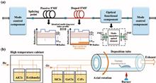
Shuailuo Huang, Lei Shen, Gang Qiao, Yuanpeng Ding, Yuyang Gao, Jian Cui, Baolong Zhu, Siyuan Liu, Mingqing Zuo, Jinglong Zhu, Lei Zhang, Jie Luo, Yongqi He, Zhangyuan Chen, and Juhao Li
Independent light propagation through one or multiple modes is commonly considered as a basic demand for mode manipulation in few-mode fiber (FMF)- or multimode fiber (MMF)-based optical systems such as transmission links, optical fiber lasers, or distributed optical fiber sensors. However, the insertion of doped-fiber amplifiers always kills the entire effort by inducing significant modal crosstalk. In this paper, we propose the design of doped-fiber amplifiers in FMF-based systems adopting identical multiple-ring-core (MRC) index profiles for both passive and doped fibers to achieve low modal crosstalk. We develop the direct-glass-transition (DGT) modified chemical vapor deposition (MCVD) processing for precise fabrication of few-mode erbium-doped fibers (FM-EDFs) with MRC profiles of both refractive index and erbium-ion doping distribution. Then, a few-mode erbium-doped-fiber amplifier (FM-EDFA) with a maximum gain of 26.08 dB and differential modal gain (DMG) of 2.3 dB is realized based on fabricated FM-EDF matched with a transmission FMF supporting four linearly polarized (LP) modes. With the insertion of the FM-EDFA, 60 + 60 km simultaneous LP01/LP11/LP21/LP02 transmission without inter-modal multiple-input multiple-output digital signal processing (MIMO-DSP) is successfully demonstrated. The proposed design of low-modal-crosstalk doped-fiber amplifiers provides, to our knowledge, new insights into mode manipulation methods in various applications.
Aug. 01, 2024Vol. 12 Issue 8 1768 (2024)
Pengtao Luo, Fengyi Chen, Ruohui Wang, and Xueguang Qiao
Rayleigh backscattering enhancement (RSE) of optical fibers is an effective means to improve the performance of distributed optical fiber sensing. Femtosecond laser direct-writing techniques have been used to modulate the fiber core for RSE. However, in-core modulation loses more transmission light, thus limiting the sensing distance. In this work, a cladding-type RSE (cl-RSE) structure is proposed, where the femtosecond laser is focused in the fiber cladding and an array of scatterers is written parallel to the core. The refractive-index modulation structure redistributes the light in the cladding, and the backward scattered light is recovered, which enhances the Rayleigh backscattered signal with almost no effect on the core light. Experimentally, it was demonstrated that in an effectual cl-RSE structure, the insertion loss was reduced to 0.00001 dB per scatterer, corresponding to the lowest value for a point scatterer to date. The cl-RSE structure accomplished measurements up to 800°C. In particular, the temperature measurement fluctuation of the cl-RSE fiber portion is only 0.00273°C after annealing. These results show that the cl-RSE structure has effective scattering enhancement, ultra-low loss, and excellent high-temperature characteristics, and has great potential for application in Rayleigh scattering-enhanced distributed fiber sensing.
Aug. 01, 2024Vol. 12 Issue 8 1813 (2024)
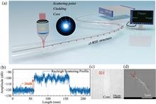
Image Processing and Image Analysis
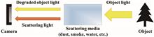
Yifu Zhou, Hanyue Wei, Jian Liang, Feiya Ma, Rui Yang, Liyong Ren, and Xuelong Li
Polarimetric dehazing is an effective way to enhance the quality of images captured in foggy weather. However, images of essential polarization parameters are vulnerable to noise, and the brightness of dehazed images is usually unstable due to different environmental illuminations. These two weaknesses reveal that current polarimetric dehazing algorithms are not robust enough to deal with different scenarios. This paper proposes a novel, to our knowledge, and robust polarimetric dehazing algorithm to enhance the quality of hazy images, where a low-rank approximation method is used to obtain low-noise polarization parameter images. Besides, in order to improve the brightness stability of the dehazed image and thus keep the image have more details within the standard dynamic range, this study proposes a multiple virtual-exposure fusion (MVEF) scheme to process the dehazed image (usually having a high dynamic range) obtained through polarimetric dehazing. Comparative experiments show that the proposed dehazing algorithm is robust and effective, which can significantly improve overall quality of hazy images captured under different environments.
Jul. 26, 2024Vol. 12 Issue 8 1640 (2024)
Imaging Systems, Microscopy, and Displays
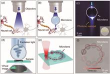
Heng Li, Xixi Chen, Tianli Wu, Zhiyong Gong, Jinghui Guo, Xiaosong Bai, Jiawei Li, Yao Zhang, Yuchao Li, and Baojun Li
Various neuromodulation techniques have been developed to modulate the peak activity of neurons, thereby regulating brain function and alleviating neurological disorders. Additionally, neuronal stimulation and imaging have significantly contributed to the understanding and treatment of these diseases. Here, we propose utilizing photonic nanojets for optical stimulation and imaging of neural cells. The application of resin microspheres as microlenses enhances fluorescence imaging of neural lysosomes, mitochondria, and actin filaments by generating photonic nanojets. Moreover, optical tweezers can precisely manipulate the microlenses to locate specific targets within the cell for real-time stimulation and imaging. The focusing capabilities of these microlenses enable subcellular-level spatial precision in stimulation, allowing highly accurate targeting of neural cells while minimizing off-target effects. Furthermore, fluorescent signals during neural cell stimulation can be detected in real-time using these microlenses. The proposed method facilitates investigation into intercellular signal transmission among neural cells, providing new insights into the underlying mechanisms of neuronal cell activities at a subcellular level.
Jul. 15, 2024Vol. 12 Issue 8 1604 (2024)
Rubing Li, Yueyun Weng, Shubin Wei, Siyuan Lin, Jin Huang, Congkuan Song, Hui Shen, Jinxuan Hou, Yu Xu, Liye Mei, Du Wang, Yujie Zou, Tailang Yin, Fuling Zhou, Qing Geng, Sheng Liu, and Cheng Lei
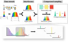
Optical time-stretch (OTS) imaging flow cytometry offers a promising solution for high-throughput and high-precision cell analysis due to its capabilities of high-speed, high-quality, and continuous imaging. Compressed sensing (CS) makes it practically applicable by significantly reducing the data volume while maintaining its high-speed and high-quality imaging properties. To enrich the information of the images acquired with CS-equipped OTS imaging flow cytometry, in this work we propose and experimentally demonstrate Fourier-domain-compressed OTS quantitative phase imaging flow cytometry. It is capable of acquiring intensity and quantitative phase images of cells simultaneously from the compressed data. To evaluate the performance of our method, static microparticles and a corn root cross section are experimentally measured under various compression ratios. Furthermore, to show how our method can be applied in practice, we utilize it in the drug response analysis of breast cancer cells. Experimental results show that our method can acquire high-quality intensity and quantitative phase images of flowing cells at a flowing speed of 1 m/s and a compression ratio of 30%. Combined with machine-learning-based image analysis, it can distinguish drug-treated and drug-untreated cells with an accuracy of over 95%. We believe our method can facilitate cell analysis in both scientific research and clinical settings where both high-throughput and high-content cell analysis is required.
Jul. 26, 2024Vol. 12 Issue 8 1627 (2024)
Instrumentation and Measurements
Light sheet microscope scanning of biointegrated microlasers for localized refractive index sensingEditors' Pick
Ross C. Cowie, and Marcel Schubert
Whispering gallery mode (WGM) microlasers are highly sensitive to localized refractive index changes allowing to link their emission spectrum to various chemical, mechanical, or physical stimuli. Microlasers recently found applications in biological studies within single cells, in three-dimensional samples such as multicellular spheroids, or in vivo. However, detailed studies of biological samples also need to account for the structural heterogeneity of tissues and live animals, therefore requiring a combination of high-resolution microscopy and laser spectroscopy. Here, we design and construct a light sheet fluorescence microscope with a coupled spectrometer for use in microlaser studies for combined high-resolution, high-speed imaging and WGM spectral analysis. The light sheet illumination profile and the decoupled geometry of excitation and emission hereby directly affect the lasing and sensing properties, mainly through geometric constraints and by light coupling effects. We demonstrate the basic working principle of microlaser spectroscopy under light sheet excitation and measure the absolute refractive index within agarose and in zebrafish tail muscle tissue. We further analyze the light coupling conditions that lead to the occurrence of two separate oscillation planes. These so-called cross modes can be scanned around the entire microlaser surface, which allows to estimate a surface-averaged refractive index profile of the microlaser environment.
Jul. 26, 2024Vol. 12 Issue 8 1673 (2024)

Hao Su, Jiawen Qiu, Junlong Li, Rong Chen, Jianbi Le, Xiaoyang Lei, Yongai Zhang, Xiongtu Zhou, Tailiang Guo, and Chaoxing Wu
Non-destructive and accurate inspection of gallium nitride light-emitting diode (GaN-LED) epitaxial wafers is important to GaN-LED technology. However, the conventional electroluminescence inspection, the photoluminescence inspection, and the automated optical inspection cannot fulfill the complex technical requirements. In this work, an inspection method and an operation system based on soft single-contact operation, namely, single-contact electroluminescence (SC-EL) inspection, are proposed. The key component of the SC-EL inspection system is a soft conductive probe with an optical fiber inside, and an AC voltage (70Vpp, 100 kHz) is applied between the probe and the ITO electrode under the LED epitaxial wafer. The proposed SC-EL inspection can measure both the electrical and optical parameters of the LED epitaxial wafer at the same time, while not causing mechanical damage to the LED epitaxial wafer. Moreover, it is demonstrated that the SC-EL inspection has a higher electroluminescence wavelength accuracy than photoluminescence inspection. The results show that the non-uniformity of SC-EL inspection is 444.64%, which is much lower than that of photoluminescence inspection. In addition, the obtained electrical parameters from SC-EL can reflect the reverse leakage current (Is) level of the LED epitaxial wafer. The proposed SC-EL inspection can ensure high inspection accuracy without causing damage to the LED epitaxial wafer, which holds promising application in LED technology.
Aug. 01, 2024Vol. 12 Issue 8 1776 (2024)
Lasers and Laser Optics
Junrui Liang, Jiangming Xu, Yanzhao Ke, Sicheng Li, Junhong He, Yidong Guo, Yang Zhang, Xiaoya Ma, Jun Ye, Xiao Li, Jinyong Leng, and Pu Zhou
A spectral programmable, continuous-wave mid-infrared (MIR) optical parametric oscillator (OPO), enabled by a self-developed high-power spectral tailorable fiber laser, was proposed and realized. While operating at a single-wavelength, the maximum idler power reached 5.53 W at 3028 nm, with a corresponding pump-to-idler conversion efficiency of 14.7%. The wavelength number switchable output was available from one to three. The single idler was tunable in a range of 528 nm (2852–3380 nm). In a dual-wavelength operation, the interval between two idlers could be flexibly tuned for 470 nm (53–523 nm), and the intensity of each channel was controllable. Triple-wavelength idler emission was realized, meanwhile exhibiting spectral custom-tailored characteristics. Furthermore, we balanced the parametric gain through the pre-modulating broadband multi-peak pump spectra, enabling a 10 dB bandwidth adjustment of the idler emission from 20 to 125 nm. This versatile mid-infrared laser, simultaneously featuring wide tuning, multi-wavelength operation, and broad bandwidth manipulation, has great application potential in composition detection, terahertz generation, and speckle-free imaging.
Jul. 15, 2024Vol. 12 Issue 8 1593 (2024)
Dexiang Zhu, Zhouyuanhang Wang, Xiangyu Xu, Wenyu Du, Wei Huang, Yan Kuai, Benli Yu, Jianzhong Zheng, Zhijia Hu, and Siqi Li
Circularly polarized lasers play a pivotal role in classical optics, nanophotonics, and quantum optical information processing, while their fabrication remains complex. This article begins with examining the interactions between stimulated emission and chiral matter, outlining a simple strategy for producing circularly polarized lasing from chiral metal-organic frameworks (MOFs), such as the zeolitic imidazolate framework (ZIF), embedded with achiral laser dyes (L/D-ZIF⊃dyes). It is found that the stimulated emission threshold and intensity are influenced by the interplay between the chiral polarization of the pump light and the inherent chirality of the MOF nanoparticles. We further present the design of a chiral vertical-cavity surface-emitting laser (VCSEL), comprising an L/D-ZIF⊃dyes solid-state film sandwiched between a high-reflectivity distributed Bragg reflector (DBR) mirror and a silver film. The cavity-based lasing exhibits higher asymmetry between emitting left-handed and right-handed polarized light compared to chiral spontaneous emission (SE) and amplified spontaneous emission (ASE), with an asymmetry value glum of approximately ±0.31. This value is nearly four-fold greater than that of SE and twice that of ASE. Our findings reveal a new approach to amplify chiral signals, promoting the comprehension and application of chiral–matter interactions, and offering a simple yet effective strategy to fabricate chiral lasers.
Jul. 26, 2024Vol. 12 Issue 8 1654 (2024)
Nonlinear Optics
Advancing large-scale thin-film PPLN nonlinear photonics with segmented tunable micro-heatersEditors' Pick
Xiaoting Li, Haochuan Li, Zhenzheng Wang, Zhaoxi Chen, Fei Ma, Ke Zhang, Wenzhao Sun, and Cheng Wang
Thin-film periodically poled lithium niobate (TF-PPLN) devices have recently gained prominence for efficient wavelength conversion processes in both classical and quantum applications. However, the patterning and poling of TF-PPLN devices today are mostly performed at chip scales, presenting a significant bottleneck for future large-scale nonlinear photonic systems that require the integration of multiple nonlinear components with consistent performance and low cost. Here, we take a pivotal step towards this goal by developing a wafer-scale TF-PPLN nonlinear photonic platform, leveraging ultraviolet stepper lithography and an automated poling process. To address the inhomogeneous broadening of the quasi-phase matching (QPM) spectrum induced by film thickness variations across the wafer, we propose and demonstrate segmented thermal optic tuning modules that can precisely adjust and align the QPM peak wavelengths in each section. Using the segmented micro-heaters, we show the successful realignment of inhomogeneously broadened multi-peak QPM spectra with up to 57% enhancement of conversion efficiency. We achieve a high normalized conversion efficiency of 3802% W-1 cm-2 in a 6 mm long PPLN waveguide, recovering 84% of the theoretically predicted efficiency in this device. The advanced fabrication techniques and segmented tuning architectures presented herein pave the way for wafer-scale integration of complex functional nonlinear photonic circuits with applications in quantum information processing, precision sensing and metrology, and low-noise-figure optical signal amplification.
Aug. 01, 2024Vol. 12 Issue 8 1703 (2024)
Optical Devices
Min Wang, Yuechen Lei, Zhi-Gang Hu, Chenghao Lao, Yuanlei Wang, Xin Zhou, Jincheng Li, Qi-Fan Yang, and Bei-Bei Li
Standing-wave supermode microresonators that are created through the strong coupling between counter-propagating modes have emerged as versatile platforms for sensing and nonlinear optics. For example, these microresonators have shown potential in nanoparticle sizing and counting, as well as enhancing the single-photon optomechanical coupling rate of stimulated Brillouin scattering. However, it has been observed that the relation between the mode linewidth and on-resonance transmission of the split supermodes differs obviously from that of the non-split modes. This behavior is typically quantified by the coupling ideality (I), which remains inadequately explored for the standing-wave supermodes. In this study, we theoretically and experimentally investigate the coupling ideality of standing-wave supermodes in a commonly employed configuration involving a SiO2 microresonator side-coupled to a tapered fiber. Our findings demonstrate that, even with a single-mode tapered fiber, the coupling ideality of the standing-wave supermodes is limited to 0.5, due to the strong backscattering-induced energy loss into the counter-propagating direction, resulting in an additional equivalent parasitic loss. While achieving a coupling ideality of 0.5 presents challenges for reaching over-coupled regimes, it offers a convenient approach for adjusting the total linewidth of the modes while maintaining critically-coupled conditions.
Jul. 15, 2024Vol. 12 Issue 8 1610 (2024)
Optoelectronics
Hui Liu, Mingyang Guo, Tian Zhang, Jian Dai, and Kun Xu
Advancements in microwave photonics have yielded novel approaches for generating high-purity microwave sources. Among these, optoelectronic oscillators (OEOs) and coupled optoelectronic oscillators (COEOs) have demonstrated the capability to generate frequency-independent microwaves with exceptionally low phase noise. Nonetheless, the tunability of the oscillators is rather limited due to the necessity for narrowband electronic bandpass filters, presenting challenges in achieving both wide and rapid tuning capabilities. Here, we present a COEO featuring ultralow phase noise, flexible tuning capability, and high robustness. This is achieved through a quiet point (QP)-operated harmonic mode-locked fiber laser, which effectively mitigates optical amplifier noise and supermode competition, thus significantly diminishing the necessity for ultra-narrow electronic filters. Due to the liberated tuning ability, we present an oscillator that can be tuned from 2 GHz to 18 GHz, with phase noise as low as -140 dBc/Hz at 10 kHz under the QP operation. We then illustrate the practical application of the proposed oscillator in generating frequency-hopping signals with consistent spurious modes less than -85 dBc, absolute phase noise below -135 dBc/Hz at 10 kHz, hopping resolution of 1.25 MHz, and fractional frequency stability below 6.1×10⁻¹² at 1 s averaging time when locked to a reference. The presented COEO structure emerges as a compelling solution for agile and low-noise microwave sources in advanced wireless communication and radar systems.
Aug. 01, 2024Vol. 12 Issue 8 1785 (2024)
Chengdong Yang, Yilong Liu, Linlin Su, Xinwei Li, Lihua Xu, and Qimei Cheng
Neuromorphic applications have shown great promise not only for efficient parallel computing mode to hold certain computational tasks, such as perception and recognition, but also as key biomimetic elements for the intelligent sensory system of next-generation robotics. However, achieving such a biomimetic nociceptor that can adaptively switch operation mode with a stimulation threshold remains a challenge. Through rational design of material properties and device structures, we realized an easily-fabricated, low-energy, and reconfigurable nociceptor. It is capable of threshold-triggered adaptive bi-mode jump that resembles the biological alarm system. With a tunnel silicon nitride (Si3N4) we mimicked the intensity- and rehearsal-triggered jump by means of the tunneling mode transition of Si3N4 dielectric. Under threshold signals the device can also express some common synaptic functions with an extremely low energy density of 33.5 fJ/μm2. In addition, through the modulation of Si3N4 thickness it is relatively easy to fabricate the device with differing pain degree. Our nociceptor analog based on a tunneling layer provides an opportunity for the analog pain alarm system and opens up a new path toward threshold-related novel applications.
Aug. 01, 2024Vol. 12 Issue 8 1820 (2024)
Physical Optics
Yutian Liang, Ruijian Li, Jie Zhao, Xingyuan Lu, Tong Liu, Zhengliang Liu, Yuan Ren, and Chengliang Zhao
There recently has been increasing interest in the research and application of the rotational Doppler effect (RDE), which paves a promising way to detect rotating objects remotely. In order to obtain more information about the rotating object from the rotational Doppler signal, composite vortex beams by coaxial superposition of orbital angular momentum (OAM) modes are often used as the probe beam. However, to the best of our knowledge, the RDE of composite vortex beams with arbitrary OAM spectra has not yet been comprehensively studied. In this paper, the correspondence between the OAM spectrum of a probe beam and the frequency spectrum of a rotational Doppler signal is theoretically analyzed. It is explicitly revealed that the RDE frequency spectrum of scattered light is related to the product of two autocorrelation functions: one from the OAM spectrum of probe beam and the other from the spiral spectrum of rotating object. On the basis of this relation, one can regulate the RDE frequency spectrum on demand via tailoring the OAM spectrum of the probe beam. As a proof of concept we design a special composite vortex beam to eliminate the broadening of the RDE spectrum induced by misalignment. These findings are of practical value in applications such as remote sensing and optical metrology.
Jul. 26, 2024Vol. 12 Issue 8 1665 (2024)
Haolin Lin, Junhui Jia, Guohua Liu, Yanwen Hu, Zhen Li, Zhenqiang Chen, and Shenhe Fu
Optical singularity states, which significantly affect propagation properties of light in free space or optical medium, can be geometrically classified into screw and edge types. These different types of singularity states do not exhibit direct connection, being decoupled from each other in the absence of external perturbations. Here we demonstrate a novel optical process in which a higher-order edge singularity state initially nested in the propagating Gaussian light field gradually involves into a screw singularity with a new-born topological charge determined by order of the edge state. The considered edge state comprises an equal superposition of oppositely charged vortex and antivortex modes. We theoretically and experimentally realize this edge-to-screw conversion process by introducing intrinsic vortex–antivortex interaction. We also present a geometrical representation for mapping this dynamical process, based on the higher-order orbital Poincaré sphere. Within this framework, the edge-to-screw conversion is explained by a mapping of state evolution from the equator to the north or south pole of the Poincaré sphere. Our demonstration provides a novel approach for manipulating singularity state by the intrinsic vortex–antivortex interactions. The presented phenomenon can be also generalized to other wave systems such as matter wave, water wave, and acoustic wave.
Jul. 26, 2024Vol. 12 Issue 8 1689 (2024)
Quantum Optics
Chengying Liu, Haibo Hu, Zhengtong Liu, Shumin Xiao, Junfeng Wang, Yu Zhou, and Qinghai Song
All-optical thermometry plays a crucial role in precision temperature measurement across diverse fields. Quantum defects in solids are one of the most promising sensors due to their excellent sensitivity, stability, and biocompatibility. Yet, it faces limitations, such as the microwave heating effect and the complexity of spectral analysis. Addressing these challenges, we introduce a novel approach to nanoscale optical thermometry using quantum defects in silicon carbide (SiC), a material compatible with complementary metal-oxide-semiconductor (CMOS) processes. This method leverages the intensity ratio between anti-Stokes and Stokes emissions from SiC color centers, overcoming the drawbacks of traditional techniques such as optically detected magnetic resonance (ODMR) and zero-phonon line (ZPL) analysis. Our technique provides a real-time, highly sensitive (1.06%K-1), and diffraction-limited temperature sensing protocol, which potentially helps enhance thermal management in the future miniaturization of electronic components.
Aug. 01, 2024Vol. 12 Issue 8 1696 (2024)
Programmable silicon-photonic quantum simulator based on a linear combination of unitariesEditors' Pick
Yue Yu, Yulin Chi, Chonghao Zhai, Jieshan Huang, Qihuang Gong, and Jianwei Wang
Simulating the dynamic evolution of physical and molecular systems in a quantum computer is of fundamental interest in many applications. The implementation of dynamics simulation requires efficient quantum algorithms. The Lie-Trotter-Suzuki approximation algorithm, also known as the Trotterization, is basic in Hamiltonian dynamics simulation. A multi-product algorithm that is a linear combination of multiple Trotterizations has been proposed to improve the approximation accuracy. However, implementing such multi-product Trotterization in quantum computers remains challenging due to the requirements of highly controllable and precise quantum entangling operations with high success probability. Here, we report a programmable integrated-photonic quantum simulator based on a linear combination of unitaries, which can be tailored for implementing the linearly combined multiple Trotterizations, and on the simulator we benchmark quantum simulation of Hamiltonian dynamics. We modify the multi-product algorithm by integrating it with oblivious amplitude amplification to simultaneously reach high simulation precision and high success probability. The quantum simulator is devised and fabricated on a large-scale silicon-photonic quantum chip, which allows the initialization, manipulation, and measurement of arbitrary four-qubit states and linearly combined unitary gates. As an example, the quantum simulator is reprogrammed to emulate the dynamics of an electron spin and nuclear spin coupled system. This work promises the practical dynamics simulations of real-world physical and molecular systems in future large-scale quantum computers.
Aug. 01, 2024Vol. 12 Issue 8 1760 (2024)
Silicon Photonics
Alessandro Brugnoni, Ali Emre Kaplan, Valerio Vitali, Kyle Bottrill, Michele Re, Periklis Petropoulos, Cosimo Lacava, and Ilaria Cristiani
Integrated semiconductor lasers represent essential building blocks for integrated optical components and circuits and their stability in frequency is fundamental for the development of numerous frontier applications and engineering tasks. When dense optical circuits are considered, the stability of integrated laser sources can be impaired by the thermal cross-talk generated by the action of neighboring components, leading to a deterioration of the long-term system performance (on the scale of seconds). In this work we show the design and the experimental characterization of a silicon nitride photonic integrated circuit (PIC) that is able to frequency stabilize 16 semiconductor lasers, simultaneously. A stabilized 50 GHz-spaced two-channel system is demonstrated through the detection of the related beating note and the stability of the resulting waveform is characterized via the use of artificially induced thermal cross-talk stimuli.
Jul. 15, 2024Vol. 12 Issue 8 1619 (2024)
Symmetric silicon microring resonator optical crossbar array for accelerated inference and training in deep learningSpotlight on Optics
Rui Tang, Shuhei Ohno, Ken Tanizawa, Kazuhiro Ikeda, Makoto Okano, Kasidit Toprasertpong, Shinichi Takagi, and Mitsuru Takenaka
Photonic integrated circuits are emerging as a promising platform for accelerating matrix multiplications in deep learning, leveraging the inherent parallel nature of light. Although various schemes have been proposed and demonstrated to realize such photonic matrix accelerators, the in situ training of artificial neural networks using photonic accelerators remains challenging due to the difficulty of direct on-chip backpropagation on a photonic chip. In this work, we propose a silicon microring resonator (MRR) optical crossbar array with a symmetric structure that allows for simple on-chip backpropagation, potentially enabling the acceleration of both the inference and training phases of deep learning. We demonstrate a 4×4 circuit on a Si-on-insulator platform and use it to perform inference tasks of a simple neural network for classifying iris flowers, achieving a classification accuracy of 93.3%. Subsequently, we train the neural network using simulated on-chip backpropagation and achieve an accuracy of 91.1% in the same inference task after training. Furthermore, we simulate a convolutional neural network for handwritten digit recognition, using a 9×9 MRR crossbar array to perform the convolution operations. This work contributes to the realization of compact and energy-efficient photonic accelerators for deep learning.
Jul. 26, 2024Vol. 12 Issue 8 1681 (2024)
Heng Chen, Hui Zhang, Jing Zhou, Chen Ma, Qian Huang, Hanxing Wang, Qinghua Ren, Nan Wang, Chengkuo Lee, and Yiming Ma
On-chip spectrometers with high compactness and portability enable new applications in scientific research and industrial development. Fourier transform (FT) spectrometers have the potential to realize a high signal-to-noise ratio. Here we propose and demonstrate a generalized design for high-performance on-chip FT spectrometers. The spectrometer is based on the dynamic in-plane reconfiguration of a waveguide coupler enabled by an integrated comb-drive actuator array. The electrostatic actuation intrinsically features ultra-low power consumption. The coupling gap is crucial to the spectral resolution. The in-plane reconfiguration surmounts the lithography accuracy limitation of the coupling gap, boosting the resolution to 0.2 nm for dual spectral spikes over a large bandwidth of 100 nm (1.5–1.6 μm) within a compact footprint of 75 μm×1000 μm. Meanwhile, the in-plane tuning range can be large enough for arbitrary wavelengths to ensure the effectiveness of spectrum reconstruction. As a result, the proposed spectrometer can be easily transplanted to other operation bands by simply scaling the structural parameters. As a proof-of-concept, a mid-infrared spectrometer is further demonstrated with a dual-spike reconstruction resolution of 1.5 nm and a bandwidth of 300 nm (4–4.3 μm).
Aug. 01, 2024Vol. 12 Issue 8 1730 (2024)
Yihao Chen, Juntao Duan, Jin Li, Yan Chen, Jiewen Li, Jianan Duan, Xiaochuan Xu, and Jiawei Wang
Whispering gallery mode optical microresonators represent a promising avenue for realizing optical analogs of coherent light–atom interactions, circumventing experimental complexities. All-optical analogs of Autler–Townes splitting have been widely demonstrated, harnessing coupled optical microresonators, also known as photonic molecules, wherein the strong coupling between resonant fields enables energy level splitting. Here, we report the characterizations of Autler–Townes splitting in waveguide-coupled microring dimers featuring mismatched sizes. By exploiting backscattering-induced coupling via Rayleigh and Mie scatterers in individual rings, high-order Autler–Townes splitting has been realized, yielding supermode hybridization in a multi-level system. Upon resonance detuning using an integrated phase shifter, intra-cavity coupling-induced splitting becomes almost indistinguishable at the zero-detuning point where the strong inter-cavity coupling counteracts the imbalance of backscattering strengths in individual rings. Through demonstrations on the maturing silicon photonics platform, our findings establish a framework of electrically tunable photonic molecules for coupling-mediated Autler–Townes splitting, offering promising prospects for on-chip signal generation and processing across classical and quantum regimes.
Aug. 01, 2024Vol. 12 Issue 8 1794 (2024)
Zhiwei Guan, Chaofeng Wang, Chuangxin Xie, Haisheng Wu, Junmin Liu, Huapeng Ye, Dianyuan Fan, Jiangnan Xiao, and Shuqing Chen
The progress of on-chip optical communication relies on integrated multi-dimensional mode (de)multiplexers to enhance communication capacity and establish comprehensive networks. However, existing multi-dimensional (de)multiplexers, involving modes and wavelengths, face limitations due to their reliance on single-directional total internal reflection and multi-level mode conversion based on directional coupling principles. These constraints restrict their potential for full-duplex functionality and highly integrated communication. We solve these problems by introducing a photonic-like crystal-connected bidirectional micro-ring resonator array (PBMRA) and apply it to duplex mode-wavelength multiplexing communication. The directional independence of total internal reflection and the cumulative effect of the subwavelength-scale pillar within the single-level photonic crystal enable bidirectional mode and wavelength multiplexed signals to transmit among multi-pair nodes without interference, improving on-chip integration in single-level mode conversion. As a proof of concept, we fabricated a nine-channel bidirectional multi-dimensional (de)multiplexer, featuring three wavelengths and three TE modes, compactly housed within a footprint of 80 μm×80 μm, which efficiently transmits QPSK-OFDM signals at a rate of 216 Gbit/s, achieving a bit error rate lower than 10-4. Leveraging the co-ring transmission characteristic and the orthogonality of the mode-wavelength channel, this (de)multiplexer also enables a doubling of communication capacity using two physical transmission channels.
Aug. 01, 2024Vol. 12 Issue 8 1802 (2024)
Kevin Zelaya, and Mohammed-Ali Miri
An integrated photonic circuit architecture to perform a modified-convolution operation based on the discrete fractional Fourier transform (DFrFT) is introduced. This is accomplished by utilizing two nonuniformly coupled waveguide lattices with equally spaced eigenmode spectra, the lengths of which are chosen so that the DFrFT and its inverse operations are achieved. A programmable modulator array is interlaced so that the required fractional convolution operation is performed. Numerical simulations demonstrate that the proposed architecture can effectively perform smoothing and edge detection tasks even for noisy input signals, which is further verified by electromagnetic wave simulations. Notably, mild lattice defects do not jeopardize the architecture performance, showing its resilience to manufacturing errors.
Aug. 01, 2024Vol. 12 Issue 8 1828 (2024)
Surface Optics and Plasmonics
Feng Xu, Yarong Yu, Yang Liu, Yao Chang, Wenxiang Jiao, Lin Wang, Hopui Ho, Bei Wu, Fei Xu, Yanqing Lu, Yuanjie Pang, and Guanghui Wang
Optical tweezers (OTs) can immobilize and manipulate objects with sizes that span between nano- and micro-meter scales. The manipulating ability of OTs is traditionally characterized by stability factor (S), which can only indicate an empirical “hit-or-miss” process. Additionally, the current quantitative models for trapping stability rarely consider the influence of external flow. In this paper, a comprehensive analysis to quantify the optical trapping stability in a perturbed asymmetric potential well is presented from the perspective of statistics, especially for weak trapping scenarios. Our analytical formulation takes experimentally measurable parameters including particle size, optical power, and spot width as inputs and precisely outputs a statistically relevant mean trapping time. Importantly, this formulation takes into account general and realistic cases including fluidic flow velocity and other perturbations. To verify the model, a back-focal-plane-interferometer-monitored trapping experiment in a flow is set up and the statistical characteristics of trapping time demonstrate good agreement with theoretical predictions. In total, the model quantitatively reveals the effects of external disturbance on trapping time, which will find applications where optical trapping stability is challenged by external perturbations in weak trapping conditions.
Aug. 01, 2024Vol. 12 Issue 8 1741 (2024)
Zhenxin Wang, Alexey V. Krasavin, Chenxinyu Pan, Junsheng Zheng, Zhiyong Li, Xin Guo, Anatoly V. Zayats, Limin Tong, and Pan Wang
Ultrathin plasmonic nanostructures offer an unparalleled opportunity for the study of light–matter interactions at the nanoscale and realization of compact nanophotonic devices. In this study, we introduce an ultrathin gold nanoribbon array and demonstrate an electric approach to actively tuning its plasmonic resonance, which leveraging the extreme light confinement capability in the ultrathin plasmonic nanostructure and a robust nanoscale electro-optical effect in indium tin oxide. Optimizing the design (to a total thickness as small as 12 nm for a 2-nm-thick gold nanoribbon array), we numerically demonstrate a spectral shift in the plasmonic resonance up to 36 nm along with an approximately 16% change in the transmission at a gate voltage below 1.7 V at the wavelength of 1.47 μm. This work presents progress towards electric tuning of plasmonic resonances in ultrathin metallic nanostructures for various applications including surface-enhanced spectroscopy, spontaneous emission enhancement, and optical modulation.
Aug. 01, 2024Vol. 12 Issue 8 1750 (2024)
Imaging Systems, Microscopy, and Displays
Zhi Li, Yaqi Han, Lican Wu, Zihan Zang, Maolin Dai, Sze Yun Set, Shinji Yamashita, Qian Li, and H. Y. Fu
Light detection and ranging (LiDAR), as a hot imaging technology in both industry and academia, has undergone rapid innovation and evolution. The current mainstream direction is towards system miniaturization and integration. There are many metrics that can be used to evaluate the performance of a LiDAR system, such as lateral resolution, ranging accuracy, stability, size, and price. Until recently, with the continuous enrichment of LiDAR application scenarios, the pursuit of imaging speed has attracted tremendous research interest. Particularly, for autonomous vehicles running on motorways or industrial automation applications, the imaging speed of LiDAR systems is a critical bottleneck. In this review, we will focus on discussing the upper speed limit of the LiDAR system. Based on the working mechanism, the limitation of optical parts on the maximum imaging speed is analyzed. The beam scanner has the greatest impact on imaging speed. We provide the working principle of current popular beam scanners used in LiDAR systems and summarize the main constraints on the scanning speed. Especially, we highlight the spectral scanning LiDAR as a new paradigm of ultrafast LiDAR. Additionally, to further improve the imaging speed, we then review the parallel detection methods, which include multiple-detector schemes and multiplexing technologies. Furthermore, we summarize the LiDAR systems with the fastest point acquisition rate reported nowadays. In the outlook, we address the current technical challenges for ultrafast LiDAR systems from different aspects and give a brief analysis of the feasibility of different approaches.
Aug. 01, 2024Vol. 12 Issue 8 1709 (2024)
© Copyright 2018-2021 | Chinese Laser Press.
All Rights Reserved 沪ICP备15018463号-20