


 View fulltext
The ultraviolet photodetectors based on the graphene/AlGaN van der Waals junction in different configurations reveal distinct response characteristics and working mechanisms, which may promote their unique applications in biomimetic visual imaging and self-powered detection in deep space. See Yuanyuan Yue et al., pp. 1858.

2024
Volume: 12 Issue 9
24 Article(s)

Holography, Gratings, and Diffraction
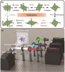
Zhi Li, Xuhao Luo, Jing Wang, Xin Yuan, Dongdong Teng, Qiang Song, and Huigao Duan
The fast algorithms in Fourier optics have invigorated multifunctional device design and advanced imaging technologies. However, the necessity for fast computations limits the widely used conventional Fourier methods, where the image plane has a fixed size at certain diffraction distances. These limitations pose challenges in intricate scaling transformations, 3D reconstructions, and full-color displays. Currently, the lack of effective solutions makes people often resort to pre-processing that compromises fidelity. In this paper, leveraging a higher-dimensional phase space method, a universal framework is proposed for customized diffraction calculation methods. Within this framework, a variable-scale diffraction computation model is established for adjusting the size of the image plane and can be operated by fast algorithms. The model’s robust variable-scale capabilities and its aberration automatic correction capability are validated for full-color holography, and high fidelity is achieved. The tomography experiments demonstrate that this model provides a superior solution for holographic 3D reconstruction. In addition, this model is applied to achieve full-color metasurface holography with near-zero crosstalk, showcasing its versatile applicability at nanoscale. Our model presents significant prospects for applications in the optics community, such as beam shaping, computer-generated holograms (CGHs), augmented reality (AR), metasurface optical elements (MOEs), and advanced holographic head-up display (HUD) systems.
Aug. 29, 2024Vol. 12 Issue 9 1937 (2024)
Imaging Systems, Microscopy, and Displays
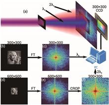
Boyang Li, Zehua Xiao, Hao Yuan, Pei Huang, Huabao Cao, Hushan Wang, Wei Zhao, and Yuxi Fu
Ultrafast imaging simultaneously pursuing high temporal and spatial resolution is a key technique to study the dynamics in the microscopic world. However, the broadband spectra of ultra-short pulses bring a major challenge to traditional coherent diffraction imaging (CDI), as they result in an indistinct diffraction pattern, thereby complicating image reconstruction. To address this, we introduce, to our knowledge, a new ultra-broadband coherent imaging method, and empirically demonstrate its efficacy in facilitating high-resolution and rapid image reconstruction of achromatic objects. The existing full bandwidth limitation for snapshot CDI is enhanced to ∼60% experimentally, restricted solely by our laser bandwidth. Simulations indicate the applicability of our method for CDI operations with a bandwidth as high as ∼140%, potentially supporting ultrafast imaging with temporal resolution into ∼50-attosecond scale. Even deployed with a comb-like harmonic spectrum encompassing multiple octaves, our method remains effective. Furthermore, we establish the capability of our approach in reconstructing a super-broadband spectrum for CDI applications with high fidelity. Given these advancements, we anticipate that our method will contribute significantly to attosecond imaging, thereby advancing cutting-edge applications in material science, quantum physics, and biological research.
Aug. 30, 2024Vol. 12 Issue 9 2068 (2024)
Instrumentation and Measurements
Chen Zhang, Yisi Dong, Pengcheng Hu, Haijin Fu, Hongxing Yang, Ruitao Yang, Yongkang Dong, Limin Zou, and Jiubin Tan
The embedded ultra-precision displacement measurement is of great interest in developing high-end equipment as well as precision metrology. However, conventional interferometers only focus on measurement accuracy neglecting the sensor volume and requirement of embedded measurement, thus hindering their broad applications. Here we present a new sensing method for realizing large-range displacement measurement in narrow space scenarios based on the combination of a fiber microprobe interference-sensing model and precision phase-generated carrier. This is achieved by microprobe tilted-axis Gaussian optical field diffraction and high-order carrier demodulation to realize large-range displacement sensing. It is uncovered that the microprobe element misalignment and phase demodulation means play pivotal roles in the interference signal and the accuracy of large-range displacement sensing. The analysis shows that the proposed interference-sensing method can effectively reduce the nonlinearities. Experimental results illustrate that the measurement range extends from 0 to 700 mm. Furthermore, the maximum nonlinear error is reduced from tens of nanometers to 0.82 nm over the full range, allowing subnanometer accuracy for embedded measurements in the hundreds of millimeters range.
Aug. 19, 2024Vol. 12 Issue 9 1877 (2024)
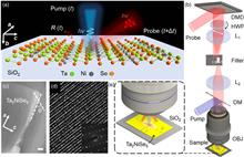
Bingxu Chen, Jie Qiao, Fei Han, Fu Feng, and Shih-Chi Chen
In two-dimensional (2D) material studies, tracking the anisotropic ultrafast carrier dynamics is essential for the development of optoelectronic nano-devices. Conventionally, the anisotropic optical and electronic properties are investigated via either polarization-dependent Raman spectroscopy or field-effect transistors measurements. However, study of the anisotropic transient carrier behaviors is still challenging, due largely to the lack of picosecond-resolved acquisition or programmable scanning capabilities in the current characterization systems. In this work, we select Ta2NiSe5 as a model system to investigate the ultrafast anisotropic transportation properties of photo-excited carriers and transient polarized responses via a digital micromirror device (DMD)-based pump-probe microscope, where the probe beam scans along the armchair and zigzag directions of a crystal structure via binary holography to obtain distinct carrier diffusion coefficients, respectively. The results reveal the nonlinear diffusion behaviors of Ta2NiSe5 in tens of picoseconds, which are attributed to the interplay between excited electrons and phonons. The trend of the measured local polarization-dependent transient reflectivity is consistent with the polarized Raman spectra results. These results show that the DMD-based pump-probe microscope is an effective and versatile tool to study the optoelectronic properties of 2D materials.
Aug. 26, 2024Vol. 12 Issue 9 1918 (2024)
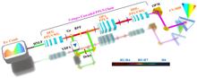
Frequency comb generation from the ultraviolet to mid-infrared region based on a three-stage cascaded PPLN chainEditors' Pick
Xiong Qin, Daping Luo, Lian Zhou, Jiayi Pan, Zejiang Deng, Gehui Xie, Chenglin Gu, and Wenxue Li
Optical frequency combs (OFCs) have enabled significant opportunities for high-precision frequency metrology and high-resolution broadband spectroscopy. Although nonlinear photonics chips have the capacity of frequency expansion for OFCs, most of them can only access the limited bandwidths in the partial infrared region, and it is still hard to satisfy many measurement applications in the ultraviolet-to-visible region. Here, we demonstrate a compact broadband OFC scheme via the combination of three χ(2) nonlinearities in a three-stage periodically poled lithium niobate (PPLN) chain. With a supercontinuum spectrum OFC delivered into the PPLN chain, the intra-pulse diffidence frequency generation, optical parametric amplification, and high-order harmonic generation were carried out in sequence. It is crucial that the harmonics of the 1st–10th orders are simultaneously obtained with an offset-free OFC spectrum from 0.35 to 4.0 μm. In view of the great potential for integration and spectral expansion, this wideband frequency comb source will open a new insight for the valuable applications of two-dimensional material analysis, biofluorescence microscopy, and nonlinear amplitude-phase metrology.
Aug. 29, 2024Vol. 12 Issue 9 2012 (2024)
Integrated Optics
Kaikai Liu, Nitesh Chauhan, Meiting Song, Mark W. Harrington, Karl D. Nelson, and Daniel J. Blumenthal
Ultra-high-quality-factor (Q) resonators are a critical component for visible to near-infrared (NIR) applications, including quantum sensing and computation, atomic timekeeping and navigation, precision metrology, microwave photonics, and fiber optic sensing and communications. Implementing such resonators in an ultra-low-loss CMOS foundry compatible photonic integration platform can enable the transitioning of critical components from the lab- to the chip-scale, such as ultra-low-linewidth lasers, optical reference cavities, scanning spectroscopy, and precision filtering. The optimal operation of these resonators must preserve the ultra-low losses and simultaneously support the desired variations in coupling over a wide range of visible and NIR wavelengths as well as provide tolerance to fabrication imperfections. We report a significant advancement in high-performance integrated resonators based on a two-point-coupling design that achieves critical coupling simultaneously at multiple wavelengths across wide wavebands and tuning of the coupling condition at any wavelength, from under-, through critically, to over-coupled. We demonstrate critical coupling at 698 nm and 780 nm in one visible-wavelength resonator and critical coupling over a wavelength range from 1550 nm to 1630 nm in a 340-million intrinsic Q 10-meter-coil waveguide resonator. Using the 340-million intrinsic Q coil resonator, we demonstrate laser stabilization that achieves six orders of magnitude reduction in the semiconductor laser frequency noise. We also report that this design can be used as a characterization technique to measure the intrinsic waveguide losses from 1300 nm to 1650 nm, resolving hydrogen-related absorption peaks at 1380 nm and 1520 nm in the resonator, giving insight to further reduce waveguide loss. The CMOS foundry compatibility of this resonator design will provide a path towards scalable system-on-chip integration for high-performance precision experiments and applications, improving reliability, and reducing size and cost.
Aug. 19, 2024Vol. 12 Issue 9 1890 (2024)

Lasers and Laser Optics
Yao Xiao, Pei Miao, Jun Wang, Heng Liu, Yudan Gou, Zhicheng Zhang, Bangguo Wang, Wuling Liu, Qijie Wang, Guoliang Deng, and Shouhuan Zhou
High-power, high-efficiency single-mode vertical-cavity surface-emitting lasers (VCSELs) are crucial in the realm of green photonics for high-speed optical communication. However, in recent years, the power and efficiency of single-mode VCSELs have remained relatively low and have been progressing slowly. This study combines theoretical models with experiments to show that multi-junction cascaded 940 nm VCSELs based on surface microstructures can achieve high power, high efficiency, and low divergence in single-mode laser output. Simulations show multi-junction VCSELs with surface microstructures can boost mode modulation capabilities, power, and efficiency, potentially allowing high-power single-mode VCSELs to surpass 60% efficiency. Using this technique, the 6 μm oxide aperture VCSELs with surface relief of different diameters were fabricated. The single-mode VCSELs with the output power of 20.2 mW, side-mode suppression ratios greater than 35 dB, 42% electro-optical efficiency, and a 9.8° divergence angle (at 1/e2) under continuous-wave operation were demonstrated. Near-field images verified its fundamental mode operation. To the best of the authors’ knowledge, this is the highest single-mode power recorded for a single-unit VCSEL to date, almost twice the currently known record, while still maintaining a very high electro-optical conversion efficiency. This research will provide valuable references for the further development and application of high-power, high-efficiency single-mode semiconductor lasers.
Aug. 26, 2024Vol. 12 Issue 9 1899 (2024)
Meiting Xie, Jiangtao Xu, Jiajun Wang, Huihui Zhao, Yeshuai Liu, Jianxiang Wen, Fufei Pang, Jianfeng Sun, and Xianglong Zeng
Cylindrical vector beams (CVBs) with special polarization distribution have been extensively investigated due to the unique ways of interacting with matter. Although several configurations have been developed to generate CVBs, such as Q-plates and subwavelength gratings, the bandwidth of a single CVB is inherently narrow due to the phase geometry, which would limit its application for femtosecond lasers. Here, a broadband CVB mode converter based on an acoustically induced fiber grating (AIFG) and a tuning method of dispersion turning point (DTP) is demonstrated both theoretically and experimentally with the 3-dB bandwidth of 125 nm, which is more than 10 times that of conventional AIFGs. Not only can the DTP wavelength be tuned from the original 1500 nm to 1650 nm by thinning the fiber, but also the stable generation of a single broadband HE21odd/even mode can be controllably implemented by adjusting the polarization state of the incident light, owing to the larger beat length difference between HE21 and other CV modes. Additionally, the femtosecond CVBs and orbital angular momentum (OAM) modes are successfully generated and amplified by combining the broadband AIFG with a figure-9 mode-locked fiber laser. Meanwhile, it is verified by simulation that the choice of broadband CV mode and the tunability of DTP wavelength can be realized by designing ring-core fibers with different structures, which can furthermore improve the flexibility of generating high purity CVBs. This study provides a highly controllable technique for the generation of broadband CVBs and OAMs paving the way for high-capacity CVBs communication.
Aug. 26, 2024Vol. 12 Issue 9 1907 (2024)
Ultrasensitive detection of remote acoustic vibrations at 300 m distance by optical feedback enhancementEditors' Pick
Mingwang Tian, Xin Xu, Sihong Chen, Zhipeng Feng, and Yidong Tan
Sensitive detection of remote vibrations at nanometer scale owns promising potential applications such as geological exploration, architecture, and public security. Nevertheless, how to detect remote vibration information with high sensitivity and anti-disturbance has become a major challenge. Reported current non-contact measurement methods are difficult to simultaneously possess characteristics of high light intensity sensitivity, long working distance, high vibration response sensitivity, and anti-disturbance of ambient light. Here, we propose a polarization-modulated laser frequency-shifted feedback interferometry method with the above characteristics, to obtain remote vibration information. The method can directly measure non-cooperative targets without the need for any cooperative markers. In each interference cycle, the energy as low as 2.3 photons can be effectively responded to, and the vibration amplitude sensitivity at 300 m can reach 0.72 nm/Hz1/2 at 1 kHz. This approach provides a strategy for the ultrasensitive detection of remote vibration that is immune to electromagnetic interference.
Aug. 29, 2024Vol. 12 Issue 9 1962 (2024)
Tiantian Shi, Qiang Wei, Xiaomin Qin, Zhenfeng Liu, Kunkun Chen, Shiying Cao, Hangbo Shi, Zijie Liu, and Jingbiao Chen
133Cs, the only stable cesium (Cs) isotope, is one of the most investigated elements in atomic spectroscopy and was used to realize the atomic clock in 1955. Among all atomic clocks, the cesium atomic clock has a special place, since the current unit of time is based on a microwave transition in the Cs atom. In addition, the long lifetime of the 6P3/2 state and simple preparation technique of Cs vapor cells have great relevance to quantum and atom optics experiments, which suggests the use of the 6S-6P D2 transition as an optical frequency standard. In this work, using one laser as the local oscillator and Cs atoms as the quantum reference, we realize two atomic clocks at the optical and microwave frequencies. Both clocks can be freely switched or simultaneously output. The optical clock, based on the vapor cell, continuously operated with a frequency stability of 3.9×10⁻¹³ at 1 s, decreasing to 2.2×10⁻¹³ at 32 s, which was frequency-stabilized by modulation transfer spectroscopy and estimated by an optical comb. Then, applying this stabilized laser to an optically pumped Cs beam atomic clock to reduce the laser frequency noise, we obtained a microwave clock with a frequency stability of 1.8×10⁻¹²/τ, reaching 6×10-15 at 105 s. This study demonstrates an attractive feature for the commercialization and deployment of optical and microwave clocks, and will guide the further development of integrated atomic clocks with better stability. Therefore, this study holds significant practical implications for future applications in satellite navigation, communication, and timing.
Aug. 29, 2024Vol. 12 Issue 9 1972 (2024)
Quantum dot fourth-harmonic colliding pulse mode-locked laser for high-power optical comb generation
Jing-Zhi Huang, Bo Yang, Jia-Jian Chen, Jia-Le Qin, Xinlun Cai, Jie Yan, Xi Xiao, Zi-Hao Wang, Ting Wang, and Jian-Jun Zhang
Quantum-dot mode-locked lasers have advantages such as high temperature stability, large optical bandwidth, and low power consumption, which make them ideal optical comb sources, especially for wavelength-division multiplexing (WDM) telecommunications, and optical I/O applications. In this work, we demonstrate an O-band quantum dot colliding pulse mode-locked laser (QD-CPML) to generate optical frequency combs with 200 GHz spacing with maximum channels of 12 within 3 dB optical bandwidth. To achieve the high output power of individual comb lines, four channel conditions are implemented at central wavelength of 1310 nm for WDM transmission experiments. Each channel exhibits more than 10 dBm output power with 200 Gb/s PAM-4 and 270 Gb/s PAM-8 modulation capability via thin-film LiNbO3 Mach–Zehnder interferometer modulator without the requirement of any optical amplifications. This high-order QD-CPML is an ideal comb source for power-efficient optical interconnects and large bandwidth optical data transmission.
Aug. 29, 2024Vol. 12 Issue 9 1991 (2024)
Neeraj Prakash, Jonathan Musgrave, Bowen Li, and Shu-Wei Huang
The fiber single-cavity dual-comb laser (SCDCL) is an emerging light-source architecture that opens up the possibility for low-complexity dual-comb pump-probe measurements. However, the fundamental trade-off between measurement speed and time resolution remains a hurdle for the widespread use of fiber SCDCLs in dual-comb pump-probe measurements. In this paper, we break this fundamental trade-off by devising an all-optical dynamic repetition rate difference (Δfrep) modulation technique. We demonstrate the dynamic Δfrep modulation in a modified version of the recently developed counterpropagating all-normal dispersion (CANDi) fiber laser. We verify that our all-optical dynamic Δfrep modulation technique does not introduce excessive relative timing jitter. In addition, the dynamic modulation mechanism is studied and validated both theoretically and experimentally. As a proof-of-principle experiment, we apply this so-called dynamic CANDi (DCANDi) fiber laser to measure the relaxation time of a semiconductor saturable absorber mirror, achieving a measurement speed and duty cycle enhancement factor of 143. DCANDi fiber laser is a promising light source for low-complexity, high-speed, high-sensitivity ultrafast dual-comb pump-probe measurements.
Aug. 30, 2024Vol. 12 Issue 9 2033 (2024)
Nonlinear Optics
Shuo Yan, Yiwei Sun, Fengchao Ni, Zhanwei Liu, Haigang Liu, and Xianfeng Chen
Image reconstruction through the opaque medium has great significance in fields of biophotonics, optical imaging, mesoscopic physics, and optical communications. Previous researches are limited in the simple linear scattering process. Here, we develop a nonlinear speckle decoder network, which can reconstruct the phase information of the fundamental frequency wave via the nonlinear scattering signal. Further, we validate the ability of our model to recover simple and complex structures by using MNIST and CIFAR data sets, respectively. We then show that the model is able to restore the image information through different sets of nonlinear diffusers and reconstruct the image of a kind of completely unseen object category. The proposed method paves the way to nonlinear scattering imaging and information encryption.
Aug. 30, 2024Vol. 12 Issue 9 2047 (2024)
Optical Devices
Huajie Liang, Hongxin Zeng, Tianchi Zhou, Hanyu Zhao, Shaokang Gu, Lin Zou, Tao Jiang, Lan Wang, Feng Lan, Shixiong Liang, Zhihong Feng, Ziqiang Yang, and Yaxin Zhang
Achieving ultra-precise wide-range terahertz (THz) phase modulation has been a long-standing challenge due to the short wavelength and sensitive phase of THz waves. This paper proposes a new ultra-high precision phase control method employing a digitally coding needle meta-chip embedded in a waveguide. The needle tips can effectively couple THz waves via the charge aggregation effect. By controlling the Schottky diodes with coding voltages, the charge on each meta-structure part can be tuned to form strong or weak resonances, producing phase shifts. Crucially, the massive charge accumulation and the sub-λ/10 distance between needle tips lead to near-field coupling among multiple tips. Therefore, modulation of the charge at each tip by multichannel coding voltages enables combined resonance tuning of THz waves, yielding a nonlinear phase superposition. Here, a meta-chip containing 8 needle meta-structure units is demonstrated, which breaks through the precision limitation of independent units and realizes super-resolution precision phase modulation similar to super-resolution imaging. In the 213–227 GHz band, we achieve a phase shift exceeding 180° with 11.25° accuracy, and a phase shift of over 170° with an accuracy of 3°. This super-resolution phase modulation strategy provides a new idea for future high-precision applications of THz integrated systems.
Aug. 19, 2024Vol. 12 Issue 9 1868 (2024)
Xin Gu, Jinlian Zhang, Shulin Ding, Xiaoshun Jiang, Bing He, and Qing Lin
An optical frequency comb, as a spectrum made of discrete and equally spaced spectral lines, is a light source with essential applications in modern technology. Cavity optomechanical systems were found to be a feasible candidate for realizing an on-chip frequency comb with low repetition rate. However, it was difficult to increase the comb line numbers of this type of frequency combs because the mechanical oscillation amplitude of such a system, which determines the frequency comb bandwidth, cannot quickly increase with pump laser power. Here, we develop a new approach to generate a broadband optomechanical frequency comb by employing a different mechanism to enhance the mechanical oscillation. Two pump tones with their frequency difference matching the mechanical frequency will drive the system into a self-organized nonlinear resonance and thus tremendously transfer the energy to the mechanical resonator. As a result, more than 10,000 or even more comb lines become available under the pump laser power of the order of milliwatts. A unique feature of the self-organized resonance is the mechanical frequency locking so that, within a certain range of the frequency difference between two drive tones, the distance between comb teeth can be locked by the two drive tones and becomes independent of any change of pump power. This property guarantees a stable repetition rate of the generated frequency comb.
Aug. 29, 2024Vol. 12 Issue 9 1981 (2024)
Ferre Vanden Kerchove, Didier Colle, Wouter Tavernier, Wim Bogaerts, and Mario Pickavet
Programmable photonic integrated circuits (PPICs) emerge as a novel technology with an enormous potential for ground-breaking innovation. Different architectures are currently being considered that dictate how waveguides should be connected to realize a broadly usable circuit. We focus on the effect of varying connectivity architectures on the routing of light. Three types of uniform meshes are studied, and we introduce a newly developed mesh that is called ring-connected straight lines. We provide an analytical formula to calculate exact distances in these meshes and introduce several metrics relating to routing to compare these meshes. We show that hexagonal tiles are the most promising, but the ring-connected straight lines architecture has a use case as well. Besides this, the effect of defect couplers is also studied. We find that the effects of these failures vary greatly by type and severity on the routability of the mesh.
Aug. 29, 2024Vol. 12 Issue 9 1999 (2024)
Kalipada Chatterjee, Jan Nedoma, Venugopal Arumuru, Subrat Sahu, Carlos Marques, and Rajan Jha
Improving the functionality of an optical sensor on a prefabricated platform relies heavily on an optical signal conditioning method that actively modulates optical signals. In this work, we present a method for active modulation of an optical sensor response that uses fiber modal interferometers integrated in parallel. Over a broad frequency range of 1 Hz to 1 kHz, the interferometers’ technology allows for adjustable amplification, attenuation, and filtering of dynamic signals. The suggested method is also used to enhance the real-time response of an optical fluid flowmeter. In order to keep tabs on different physical fields, the suggested approach promotes the creation of self-conditioning sensing systems.
Aug. 30, 2024Vol. 12 Issue 9 2018 (2024)
Optoelectronics
Linlin Shi, Ziyang Zhao, Jinyang Jiao, Ting Ji, Wenyan Wang, Yanxia Cui, and Guohui Li
The layered two-dimensional material tungsten diselenide (WSe2) has triggered tremendous interests in the field of optoelectronic devices due to its exceptional carrier transport property. Nevertheless, the limited absorption of WSe2 in the near infrared (NIR) band poses a challenge for the application of WSe2 photodetectors in night vision, telecommunication, etc. Herein, the enhanced performance of the WSe2 photodetector is demonstrated through the incorporation of titanium nitride nanoparticles (TiN NPs), complemented by an atomically-thick Al2O3 layer that aids in suppressing the dark current. It is demonstrated that TiN NPs can dramatically enhance the absorption of light in the proposed WSe2 photodetector in the NIR regime. This enhancement boosts photocurrent responses through the generation of plasmonic hot electrons, leading to external quantum efficiency (EQE) enhancement factors of 379.66% at 850 nm and 178.47% at 1550 nm. This work presents, for the first time, to our knowledge, that the WSe2 photodetector is capable of detecting broadband light spanning from ultraviolet to the telecommunication range, all achieved without the reliance on additional semiconductor materials. This achievement opens avenues for the advancement of cost-effective NIR photodetectors.
Aug. 13, 2024Vol. 12 Issue 9 1846 (2024)
Yuanyuan Yue, Yang Chen, Jianhua Jiang, Lin Yao, Haiyu Wang, Shanli Zhang, Yuping Jia, Ke Jiang, Xiaojuan Sun, and Dabing Li
Two-dimensional (2D) graphene has emerged as an excellent partner for solving the scarcity of ultraviolet photodetectors based on three-dimensional (3D) AlGaN, in which the design of a 2D graphene/3D AlGaN junction becomes crucial. This study investigates the response mechanisms of two distinct graphene/AlGaN (Gr-AlGaN) photodetectors in the lateral and vertical configurations. For the lateral Gr-AlGaN photodetector, photogenerated electrons drifting into p-type graphene channel induce negative photoconductivity and a persistent photoconductive effect, resulting in a high responsivity of 1.27×10⁴ A/W and detectivity of 3.88×10¹² Jones. Although the response capability of a vertical Gr-AlGaN device is inferior to the lateral one, it shows significantly reduced dark current and self-powered detection. The photogenerated electron-hole pair can be spontaneously separated by the junction electric field and generate a photocurrent at zero bias. Hence, the vertical Gr-AlGaN photodetector array is satisfied for passive driving imaging like deep space detection. Conversely, the exceptional response of the lateral Gr-AlGaN device emphasizes its prospects for steady object recognition with low-light emission. Moreover, the improved imaging sharpness with light illumination duration makes it suitable for biomimetic visual learning, which follows a recognition to memory process. This study elucidates an efficient approach for diverse photodetection applications through the configuration design of Gr-AlGaN junctions.
Aug. 13, 2024Vol. 12 Issue 9 1858 (2024)
Manipulating exciton confinement for stable and efficient flexible quantum dot light-emitting diodesSpotlight on Optics
Xiaoyun Hu, Jianfang Yang, Yufei Tu, Zhen Su, Fei Zhu, Qingqing Guan, and Zhiwei Ma
Flexible quantum dot light-emitting diodes (QLEDs) show great promise for the next generation of flexible, wearable, and artificial intelligence display applications. However, the performance of flexible QLEDs still lags behind that of rigid substrate devices, hindering their commercialization for display applications. Here we report the superior performance of flexible QLEDs based on efficient red ZnCdSe/ZnS/ZnSe QDs (A-QDs) with anti-type-I nanostructures. We reveal that using ZnS as an intermediate shell can effectively confine the exciton wavefunction to the inner core, reducing the surface sensitivity of the QDs and maintaining its excellent emission properties. These flexible QLEDs exhibit a peak external quantum efficiency of 23.0% and a long lifetime of 63,050 h, respectively. The anti-type-I nanostructure of A-QDs in the device simultaneously suppresses defect-induced nonradiative recombination and balances carrier injection, achieving the most excellent performance of flexible QLEDs ever reported. This study provides new insights into achieving superior performance in flexible QD-based electroluminescent devices.
Aug. 26, 2024Vol. 12 Issue 9 1927 (2024)
Physical Optics
Jinqi Song, Fengqi Liu, Mingli Sun, Xiangyu Tong, Naichen Zhang, Bingsong Cao, Wenzhe Wang, Kaikai Huang, Xian Zhang, and Xuanhui Lu
The dynamics of wave packets carrying a spatiotemporal vortex in the spatial fractional system is still an open problem. The difficulty stems from the fact that the fractional Laplacian derivative is essentially a nonlocal operator, and the vortex is space-time coupled. Here, we investigate the transmission of spatiotemporal vortices in the spatial fractional wave equation (FWE) and demonstrate the effects of linewidth, vortex topological charge, and linear chirp modulation on the transmission of Bessel-type spatiotemporal vortex pulses (BSTVPs). Under narrowband conditions, we find that the propagation of BSTVP in the FWE can be seen as the coherent superposition of two linearly shifted half-BSTVPs and can reveal orbital angular momentum backflow for the half-BSTVP. Our analysis can be extended to other spatiotemporal vortex pulses.
Aug. 30, 2024Vol. 12 Issue 9 2027 (2024)
Silicon Photonics
Shahrzad Khajavi, Jianhao Zhang, Pavel Cheben, Daniele Melati, Jens H. Schmid, Ross Cheriton, Martin Vachon, Shurui Wang, Ahmad Atieh, Carlos Alonso Ramos, and Winnie N. Ye
Optical antennas play a pivotal role in interfacing integrated photonic circuits with free-space systems. Designing antennas for optical phased arrays ideally requires achieving compact antenna apertures, wide radiation angles, and high radiation efficiency all at once, which presents a significant challenge. Here, we experimentally demonstrate a novel ultra-compact silicon grating antenna, utilizing subwavelength grating nanostructures arranged in a transversally interleaved topology to control the antenna radiation pattern. Through near-field phase engineering, we increase the antenna’s far-field beam width beyond the Fraunhofer limit for a given aperture size. The antenna incorporates a single-etch grating and a Bragg reflector implemented on a 300-nm-thick silicon-on-insulator (SOI) platform. Experimental characterizations demonstrate a beam width of 44°×52° with -3.22 dB diffraction efficiency, for an aperture size of 3.4 μm×1.78 μm. Furthermore, to the best of our knowledge, a novel topology of a 2D antenna array is demonstrated for the first time, leveraging evanescently coupled architecture to yield a very compact antenna array. We validated the functionality of our antenna design through its integration into this new 2D array topology. Specifically, we demonstrate a small proof-of-concept two-dimensional optical phased array with 2×4 elements and a wide beam steering range of 19.3º × 39.7º. A path towards scalability and larger-scale integration is also demonstrated on the antenna array of 8×20 elements with a transverse beam steering of 31.4º.
Aug. 29, 2024Vol. 12 Issue 9 1954 (2024)
Surface Optics and Plasmonics
Ying Wang, Shibiao Wei, Zhendong Ju, Changjun Min, Michael Somekh, and Xiaocong Yuan
Optical trapping has revolutionized various scientific disciplines with its non-invasive, high-resolution manipulation capabilities. However, conventional optical tweezers face limitations in effectively manipulating metallic particles due to their high reflectivity and associated scattering forces. Plasmonic tweezers, harnessing surface plasmons in metallic nanostructures, offer a promising solution by confining light to deep subwavelength scales and enhancing optical forces. However, dynamically manipulating metallic particles with plasmonic tweezers without mechanical adjustments remains a significant challenge. In this paper, we propose a novel approach utilizing dynamic optical tweezers with tunable plasmonic fields for metallic particle manipulation. By dynamically tailoring plasmonic fields with holograms, metallic particles can be manipulated without mechanical adjustments. Finite-difference time-domain simulations and Maxwell stress tensor calculations demonstrate the effectiveness of this technique, which offers simplicity, precision, and motionlessness in metallic particle manipulation. This advancement holds promise for applications in surface-enhanced Raman scattering, biosensing, super-resolved detection, and nanoparticle assembly, opening new avenues in plasmonic tweezers technology.
Aug. 13, 2024Vol. 12 Issue 9 1840 (2024)
Shuang Peng, Fei Yang, Han Zhang, Zhan Yi Fu, Chen Xi Liu, Hai Ying Lu, Ya Ting Xie, Qian Yu, Rui Huang, Xiao Jian Fu, and Jun Wei Wu
The dynamic and integrated control of near- and far-field electromagnetic waves is essential for advancing emerging intelligent information technology. Metasurfaces, distinguished by their low-profile design, cost-effectiveness, and ease of fabrication, have successfully revolutionized various electromagnetic functions. However, current research on the dynamic integrated manipulation of near-field and far-field electromagnetic waves using a single metasurface remains relatively constrained, due to the complexity of element-level control, restricted dynamic tuning range, and tuning speed. Herein, we propose an element-level controlled, versatile, compact, and broadband platform allowing for the real-time electronic reconstruction of desired near/far-field electromagnetic wavefronts. This concept is achieved by precisely regulating the 1-bit amplitude coding pattern across a guided-wave-excited metasurface aperture loaded with PIN diodes, following our binary-amplitude holographic theory and modified Gerchberg–Saxton (G–S) algorithm. Consistent findings across calculations, simulations, and experiments highlight the metasurface’s robust performance in 2D beam scanning, frequency scanning, dynamic focusing lens, dynamic holography display, and 3D multiplexing holography, even under 1-bit control. This simplified and innovative metasurface architecture holds the promise of substantially propelling forthcoming investigations and applications of highly integrated, multifunctional, and intelligent platforms.
Aug. 30, 2024Vol. 12 Issue 9 2056 (2024)
© Copyright 2018-2021 | Chinese Laser Press.
All Rights Reserved 沪ICP备15018463号-20