 View fulltext
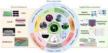
Erbium-doped/erbium-ytterbium co-doped waveguide amplifiers (EDWAs/EYCDWAs) have received much attention as essential components within large-scale functionalized silicon-based optoelectronic (SBO) chips for their remarkable ability to amplify optical signals on-chip at the communication band combined with their potential application across diverse fields. We reviewed the research progress of EDWAs/EYCDWAs comprehensively. In particular, the research advancements concerning amplifiers constructed with diverse host materials are introduced in detail, and the gain limitations of the waveguide amplifiers are thoroughly analyzed from multiple perspectives, such as host materials and innovative structural designs. Subsequently, the preparation processes of the gain medium and waveguide structure in EDWAs/EYCDWAs are discussed, and their common application scenarios and commercial applications are summarized. In addition, an assessment is carried out on the challenges encountered by EDWAs/EYCDWAs. Finally, a discussion is held on their potential applications and development prospects in the field of SBO chips, with the aspiration of providing valuable references for the development of EDWAs/EYCDWAs.
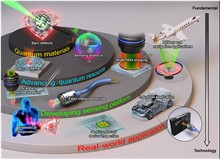
Quantum sensing aims to detect signals with unparalleled sensitivity, potentially surpassing classical limitations. Solid-state spin defects, particularly nitrogen-vacancy centers in diamond, have emerged as promising platforms due to their long coherence time, optical addressability, high field sensitivity, and spatial and spectral resolution, making them ideal for sensing and imaging applications. Their compact size and robust performance under room temperature and ambient conditions further enhance their suitability for real-world applications. We provide an overview of quantum sensing principles and explore efforts to improve sensor functionality, including advanced sensing protocols, spatial imaging techniques, and integration with optical systems to enhance detection efficiency. We also highlight recent progress in the applications of these sensors across various use cases, including biomedical diagnostics, semiconductor device inspection, and industrial and military applications.
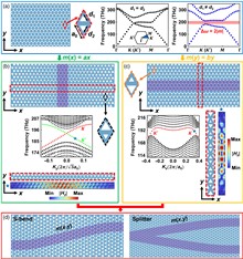
Pseudomagnetic fields (PMFs) can manipulate photons in a similar way that magnetic fields control electrons. However, the PMF-based control over light has been restricted to simple waveguiding of the Landau level states, which hinders the application of PMFs in practical photonic integrated circuits. Here, we propose a universal and systematic methodology to design complex nonuniform PMFs and arbitrarily control the flow of light in silicon photonic crystals at telecommunication wavelengths. As proofs of concept, an S-bend (with a low insertion loss of <1.83 dB) and a 50:50 power splitter (with a low excess loss of <2.11 dB and imbalance of less than ±0.5 dB) based on PMFs are experimentally demonstrated. A high-speed data transmission experiment is performed on these devices with 140-Gb / s four-level pulse amplitude modulation signals to prove their applicability in real communication systems. The proposed method offers a paradigm for exploring magnetic-field-related physics with neutral particles and developing nanophotonic devices with PMF-induced states beyond the Landau level states and the topological edge states.
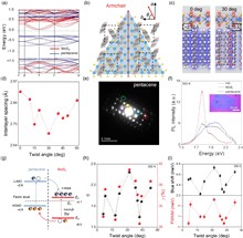
In two-dimensional (2D) organic–inorganic (O-I) heterostructures, interlayer coupling has emerged as a design parameter for engineering their electronic and optoelectronic properties, essential for designing future excitonic and optoelectronic devices. However, the further exploration of interlayer couplings is limited by their weak strength and ineffective tuning strategies, due to the inconsistent material quality and the bulky size of organic counterparts. Here, we integrate 2D pentacene single crystals with monolayer MoS2 to achieve strong interlayer coupling and effective tuning through a twisting method. We confirm this strong coupling through calculated lower interlayer spacing (∼2.70 Å), high charge transfer efficiency (∼61 % ), and a high coupling strength of ∼2.72 at a twist angle of ∼32 deg. Both density functional theory calculations and experimental results demonstrate the remarkable electrical control over interlayer couplings by adjusting electrical band alignments. This control over interlayer couplings helps to untangle the diffusion of neutral excitons and trions, which have diffusion lengths of ∼1.95 and 0.93 μm, respectively. Our results underscore the significant tunability of interlayer couplings and relaxations within O-I systems via twist angles, offering avenues for developing high-performance vertical transistors, logic devices, photodetectors, and photovoltaic devices.
High-quality and real-time holographic imaging based on dynamically tunable metasurfaces has attracted immense interest. Despite remarkable progress, the complex electrical pattern designs and slow-speed near-field scanning terahertz (THz) microscopy systems have significantly hindered the development of real-time electrically tunable metasurface holography in the THz band. We propose and experimentally demonstrate an electrically tunable vanadium dioxide (VO2)-based active metasurface that can generate real-time bias-controlled holographic information via a THz focal plane imaging system. By elaborately designing “microladders” integrated with VO2 pads, the device exhibits low power consumption (∼0.8 W) and real-time imaging (∼4.5 s). The quantitative method is theoretically utilized to investigate the thermal parameters dependent thermodynamics of the “ladder” metasurface based on theoretical analysis with the aid of thermal modelling. The calculated dynamic response time based on the quantitative thermodynamic model agrees well with experimental results. Our study can be used to propel the development of THz electrically tunable metasurfaces for low-power-consumption dynamic, real-time displays, and information encryption, providing crucial insights for future optimization of VO2-based electrothermally tunable holographic metasurfaces.
The commentary discusses a recent report of metasurface-enhanced infrared photothermal (MEIP) microscopy, which simultaneously overcomes long-standing sensitivity and spatial resolution barriers in midinfrared spectroscopy, advancing detection sensitivity to the nanomolar level.
In the past two decades, optogenetic technology has developed to be the most accurate method for investigating or treating neural correlated diseases. Currently, the applications of optogenetic technology have been expanded from the initial central nervous system to the peripheral nervous system, circulatory system, locomotor system, alimentary system, urinary system, and so on. We summarize the recent progress of optogenetic technology in biomedical applications through two categories: activation or inhibition of neural impulses. The involved diseases include Alzheimer’s disease, ischemic stroke, Parkinson’s disease, epilepsy, spinal cord injury, cardiac arrhythmias, and chronic kidney disease. Furthermore, basic and clinical research in optogenetic technology for visual restoration is highlighted, and the challenges of optogenetic technology for clinical applications are discussed.
Computational imaging (CI) leverages the joint optimization of optical system design and reconstruction algorithms, enabling superior performance in terms of dimensionality, resolution, efficiency, and hardware complexity. It has found widespread applications in medical diagnosis and astronomy, among others. Recently, deep learning (DL) has changed the paradigm of CI by harnessing learned priors from data through trained neural network models. However, widely used data-driven DL-based CI methods encounter difficulties related to training data acquisition, computation requirements, generalization, and interpretability. Recent studies have indicated that integrating the physics prior of the CI system into various components of DL pipelines (including training data, network design, and loss functions) holds promise for alleviating these challenges. To provide readers with a better understanding of the current research status and ideas, we present an overview of the state-of-the-art in DL-based CI. We begin by briefly introducing the concepts of CI and DL, followed by a comprehensive review of how DL addresses inverse problems in CI. Particularly, we focus on the emerging physics-enhanced approaches. We highlight the perspectives of future research directions and the transfer to real-world applications.
Quantum theory of photons based on the first quantization technique, similar to that used by Schrödinger in the formulation of quantum mechanics, is considered. First, scalar quantum mechanics of photons operating with the photon wave functions is discussed. Using the first quantization, the wave equation, the Schrödinger-like equations, and the Dirac equation for photons are derived. Then, vector quantum mechanics of photons is introduced, which defines the electromagnetic vector fields. Using the first quantization, the Maxwell equations for photons in a magneto-dielectric medium are obtained. Because the photon’s electric and magnetic fields satisfy the Maxwell equations, all that is known about the classical optical fields can be directly transferred to photons demonstrating their quantum diversity. Relationships between the scalar and vector quantum mechanics of photons and between the Dirac and Maxwell equations are analyzed. To describe the propagation of photons in dispersive media, modified Maxwell equations are introduced.
Infrared spectroscopy with its rich vibrational information plays a crucial role in biochemical sensing. Metasurface-enhanced infrared spectroscopy amplifies the detection sensitivity by enhancing local electromagnetic fields. However, conventional far-field techniques lack the spatial resolution to image the optical response of a single plasmonic nanostructure. In this work, we introduce mid-infrared (mid-IR) photothermal microscopy to map the hot spot distribution and thermal response of a plasmonic metasurface resonant in the mid-IR spectral range. We demonstrate infrared photothermal detection of proteins and drug molecules around a single nanoantenna. Our metasurface-enhanced infrared photothermal microscope achieves a detection limit as low as 0.24 monolayer surface coverage of bovine serum albumin, paving the way for high-throughput, highly sensitive mid-IR analysis of low-abundance molecules.
Visible optical frequency combs are essential to optical atomic clocks, astronomical spectrograph calibration, and biological imaging. However, due to the limitations of the dispersion properties of available materials and the Q-factors of the optical microresonators working at visible wavelengths, the generation of the visible soliton microcomb remains highly challenging. Here, we demonstrate a chip-based visible single-soliton microcomb spanning two-thirds of an octave (ranging from 632.5 to 950.1 nm) by precisely engineering the dispersion of a silica microdisk resonator. Two dispersion waves at the spectrum edges are created by simultaneously employing the higher order dispersion and mode interaction in a microresonator. In particular, we achieve a high Q-factor with small mode volume at the short wavelength, which facilitates the generation of the visible soliton microcombs with 1.1 mW pump power. Moreover, based on the soliton self-frequency shift, we implement a precise adjustment of the dispersive wave, which makes the highest power tooth within the dispersive wave access the transition of Sr88 + for the application in optical atomic clocks.
Quantum-confined Stark effects (QCSEs), where external or built-in electric fields modify optical transition energies, have garnered significant interest due to their potential for tuning emission energies to couple with quantum dots, metasurfaces, cavities, etc. However, only external electric-field-enabled QCSEs in 2D semiconductors have been reported so far, owing to the challenges posed by small and uncontrollable built-in electric fields, as well as charge modulation effects. We report the first observation of giant built-in electric field-enabled QCSEs in 1L WSe2 / 1L graphene heterostructure (HS) with an air-gap structure that suppresses graphene screening and bandgap renormalization. Electrical control of QCSEs demonstrates a maximum Stark shift of ∼56.97 meV. This significant shift is attributed to enhanced built-in electric fields resulting from the doping-induced increase of chemical potential difference. While increasing optical doping or reducing the interlayer distance, QCSEs weaken due to reduced built-in electric fields. By leveraging efficient exciton dissociations from built-in electric fields, the responsivity (R) and response speed of HS photodetectors increase by 3 orders of magnitude and threefold, respectively, compared with 1L WSe2. Our results offer a new avenue for enhancing exciton tunability and exploring device applications of 2D materials in photodetectors, polariton transistors, and quantum light sources.
Holography plays a crucial role in optics, yet traditional methods require complex setups and bulky devices, being unfavourable for optical integration. Although metasurface-based holograms can be ultra-compact, holographic images generated by previously realized metadevices were mostly scalar ones, with a few vectorial holograms realized so far suffering from restrictions on efficiency, incident polarization, and resolution. We propose and experimentally demonstrate an efficient meta-platform to generate vectorial holographic images with high resolutions under arbitrary incident polarizations. Combining Gerchberg–Saxton algorithm and the wave-decomposition technique, we establish a generic strategy to retrieve the optical properties (e.g., reflection phases and polarization-conversion capabilities) of meta-atoms required to construct a metasurface for generating a predesigned vectorial holographic image under a predesigned incident polarization. We next design a series of high-efficiency and deep-subwavelength single-structure meta-atoms exhibiting tailored reflection phases and polarization-conversion capabilities governed by both structural resonances and the Pancharatnam–Berry effect, and experimentally characterize their optical scattering properties. We finally construct a series of ultra-thin metadevices with these meta-atoms and experimentally demonstrate that they can generate pre-designed vectorial holographic images under illuminations of circularly polarized light at 1064 nm. We provide a highly efficient and ultra-thin platform to generate predesigned vectorial holographic images under illuminations of light with arbitrary given polarization, which can inspire numerous future applications in on-chip photonics.
Robust three-dimensional (3D) recognition across different viewing angles is crucial for dynamic applications such as autonomous navigation and augmented reality; however, the application of the technology remains challenging owing to factors such as orientation, deformation, and noise. Wave-based analogous computing, particularly diffraction neural networks (DNNs), constitutes a scan-free, energy-efficient means of mitigating these issues with strong resilience to environmental disturbances. Herein, we present a real-time all-directional 3D object recognition and distortion correction system using a deep knowledge prior DNN. Our approach effectively addressed complex two-dimensional (2D) and 3D distortions by optimizing the metasurface parameters with minimal training data and refining them using DNNs. Experimental results demonstrate that the system can effectively rectify distortions and recognize objects in real time, even under varying perspectives and multiple complex distortions. In 3D recognition, the prior DNN reliably identifies both dynamic and static objects, maintaining stable performance despite arbitrary orientation changes, highlighting its adaptability to complex and dynamic environments. Our system can function either as a preprocessing tool for imaging platforms or as a stand-alone solution, facilitating 3D recognition tasks such as motion sensing and facial recognition. It offers a scalable solution for high-speed recognition tasks in dynamic and resource-constrained applications.
All-inorganic CsPbBr3 perovskite polycrystalline films, renowned for their remarkable optoelectronic properties, solution processability, and enhanced stability over organic–inorganic counterparts, are emerging as next-generation gain media for high-performance lasers. However, due to the limited understanding of how to realize population inversion under slow carrier injection, and a lack of convenient strategies to suppress Auger recombination while retaining low optical loss, achieving high-performance quasi-continuous-wave (quasi-CW) or CW lasing based on CsPbBr3 films at ambient temperature is still challenging. We devised a phase reconstruction strategy employing volatile ammonium, which achieves substantial suppression of Auger recombination through elimination of low-dimensional phase impurities and remains low optical loss via precisely controlled film crystallization dynamics. Importantly, this strategy emphasizes the critical role of Auger recombination suppression for high-performance lasing under slower carrier injection. Ultimately, an ultralow amplified spontaneous emission threshold of 9.6 μJ cm - 2 was achieved under quasi-continuous nanosecond-pulsed excitation, which facilitated the realization of a single-mode vertical-cavity surface-emitting laser with a threshold of 17.3 μJ cm - 2 and a quality factor of 3850 under quasi-CW pumping. We represent the exceptional performance of quasi-CW lasing to date, offering valuable insights for future advancements in high-performance CW lasing and even electrically driven lasers.
Convolutional operations are computationally intensive in artificial intelligence (AI) services, and their overhead in electronic hardware limits machine learning scaling. Here, we introduce a photonic joint transform correlator (pJTC) using a near-energy-free on-chip Fourier transformation to accelerate convolution operations. The pJTC reduces computational complexity for both convolution and cross-correlation from O ( N4 ) to O ( N2 ) , where N2 is the input data size. Demonstrating functional Fourier transforms and convolution, this pJTC achieves 98.0% accuracy on an exemplary Modified National Institute of Standards and Technology inference task. Furthermore, a wavelength-multiplexed pJTC architecture shows potential for high throughput and energy efficiency, reaching 305 TOPS / W and 40.2 TOPS / mm2, based on currently available foundry processes. An efficient, compact, and low-latency convolution accelerator promises to advance next-generation AI capabilities across edge demands, high-performance computing, and cloud services.
The article provides information about the image on the cover of Advanced Photonics, Volume 7 Issue 4.
The authors comment on a recent significant advancement in developing a chiral sensor that is both sensitive and robust.
The commentary discusses recently published design for antireflective coating on solar cells. The proposed free-form inverse design, based on single-layer silicon metasurfaces, dramatically suppresses broadband optical reflection from silicon surfaces.
Optical vortices, characterized by their infinite orthogonal eigenmodes—such as orbital angular momentum (OAM) and cylindrical vector beam (CVB) modes—offer unprecedented opportunities for advancing optical communication systems. The core components of these systems—mode (de)modulation, mode processing, and mode transmission—are fundamental to the construction and networking of OAM/CVB mode-based communication networks. They significantly influence signal encoding, enhance channel capacity, and facilitate signal interconnection and transmission. We explore the historical development and recent advancements in optical vortex-based communication systems from these three critical perspectives. We systematically summarize the normative definitions and research progress related to key concepts such as mode multiplexing and routing. We also demonstrate the performance of these systems in terms of communication capacity, bit error rate, and more. Furthermore, we examine the substantial challenges and future prospects in this field, with the aim of offering cutting-edge insights that will facilitate the advancement and practical implementation of optical communication networks leveraging optical vortex modes.
Photonics has proven to be a very attractive platform for quantum technologies, offering key features such as high-fidelity qubits and room-temperature signal processing. Advancements in integrated photonics are expected to further enhance these capabilities as the technology evolves from few-photon architectures to systems capable of generating and processing tens, possibly hundreds, of photons, marking critical progress toward scalable quantum information processing. Although each integrated platform has its own unique advantages and limitations, thin-film lithium niobate (TFLN) photonics has recently emerged as a strong contender thanks to its low-loss characteristics, large electro-optic and nonlinear coefficients, broad transparency window, and ultra-fast modulation capabilities. In this review, we examine the latest developments in TFLN quantum photonics and identify promising directions and challenges for future research in this field.
Spatial photonic Ising machines (SPIMs) are promising computation devices that can be used to find the ground states of different spin Hamiltonians and solve large-scale optimization problems. The photonic architecture leverages the matrix multiplexing ability of light to accelerate the computing of spin Hamiltonian via free space light transform. However, the intrinsic long-range nature of spatial light only allows for uncontrolled all-to-all spin interaction. We explore the ability to establish arbitrary spin Hamiltonian by modulating the momentum of light. Arbitrary displacement-dependent spin interactions can be computed from different momenta of light, formulating as a generalized Plancherel theorem, which allows us to implement a SPIM with a minimal optical operation (that is, a single Fourier transform) to obtain the Hamiltonian of customized spin interaction. Experimentally, we unveil the exotic magnetic phase diagram of the generalized J1-J2-J3 model, shedding light on the ab initio magnetic states of iron chalcogenides. Moreover, we observe Berezinskii-Kosterlitz-Thouless dynamics by implementing an XY model. We open an avenue to controlling arbitrary spin interaction from the momentum space of light, offering a promising method for on-demand spin model simulation with a simple spatial light platform.
Twisted optical fibers are a promising platform for manipulating circularly polarized light and orbital angular momentum beams for applications such as nonlinear frequency conversion, optical communication, or chiral sensing. However, integration into chip-scale technology is challenging because twisted fibers are incompatible with planar photonics and the achieved twist rates are limited. Here, we address these challenges by introducing the concept of 3D-nanoprinted on-chip twisted hollow-core light cages. We show theoretically and experimentally that the geometrical twisting of light cages forces the fundamental core mode of a given handedness to couple with selected higher-order core modes, resulting in strong circular dichroism (CD). These chiral resonances result from the angular momentum harmonics of the fundamental mode, allowing us to predict their spectral locations and the occurrence of circular birefringence. Twisted light cages enable very high twist rates and CD, exceeding those of twisted hollow-core fibers by more than two orders of magnitude (twist period, 90 μm; CD, 0.8 dB / mm). Moreover, the unique cage design provides lateral access to the central core region, enabling future applications in chiral spectroscopy. Therefore, the presented concept opens a path for translating twisted fiber research to on-chip technology, resulting in a new platform for integrated chiral photonics.
Optical neural networks have emerged as feasible alternatives to their electronic counterparts, offering significant benefits such as low power consumption, low latency, and high parallelism. However, the realization of ultra-compact nonlinear deep neural networks and multi-thread processing remain crucial challenges for optical computing. We present a monolithically integrated all-optical nonlinear diffractive deep neural network (AON-D2NN) chip for the first time. The all-optical nonlinear activation function is implemented using germanium microstructures, which provide low loss and are compatible with the standard silicon photonics fabrication process. Assisted by the germanium activation function, the classification accuracy is improved by 9.1% for four-classification tasks. In addition, the chip’s reconfigurability enables multi-task learning in situ via an innovative cross-training algorithm, yielding two task-specific inference results with accuracies of 95% and 96%, respectively. Furthermore, leveraging the wavelength-dependent response of the chip, the multi-thread nonlinear optical neural network is implemented for the first time, capable of handling two different tasks in parallel. The proposed AON-D2NN contains three hidden layers with a footprint of only 0.73 mm2. It can achieve ultra-low latency (172 ps), paving the path for realizing high-performance optical neural networks.
Recent progress in direct photodetection of light orbital angular momentum (OAM) based on the orbital photogalvanic effect (OPGE) provides an effective way for on-chip direct electric readout of orbital angular momentum, as well as large-scale integration focal-plane array devices. However, the recognition of OAM order from photocurrent response requires the extraction of circular polarization-dependent response. To date, the operation speed of such a detector is currently at the minute level and is limited by slow mechanical polarization modulation and low OAM recognition capability. We demonstrate that the operation speed can be greatly improved via an electrical polarization modulation strategy with a photoelastic modulator (PEM) accompanied by a phase-locked readout approach with a lock-in amplifier. We demonstrate an operation speed of up to kilohertz level with this new technology in the mid-infrared region (4 μm) on an OAM detector using multilayer graphene as photosensitive material. In principle, with a new modulation and readout scheme, we can potentially increase the operation speed to megahertz with a PEM that operates at a state-of-the-art speed. Our work paves the way toward high-speed operation of direct OAM detection devices based on the OPGE effect and pushes such technology to a more practical stage for focal plane array applications.
Flatbands are of significant interest due to their potential for strong energy confinement and their ability to facilitate strongly correlated physics such as unconventional superconductivity and fractional quantum Hall states. When topology is incorporated into flatband systems, it further enhances flatband mode robustness against perturbations. We present the first realization of doubly degenerate topological flatbands of edge states in chiral-symmetric strained graphene. The flatband degeneracy stems from the merging of Dirac points, achieved by tuning the coupling ratios in a honeycomb lattice with newly discovered twig boundary conditions. The topology of these modes is characterized by the nontrivial winding number, which ensures their robustness against disorder. Experimentally, two types of topological edge states are observed in a strained photonic graphene lattice, consistent with numerical simulations. Moreover, the degeneracy of the topological flatbands doubles the density of states for zero-energy modes, facilitating the formation of compact edge states and providing greater control over edge states and light confinement. Our findings underscore the interplay among lattice geometry, symmetry, and topology in shaping doubly degenerate topological flatbands. This work opens new possibilities for advancements in correlated effects, nonlinear optical phenomena, and efficient energy transfer in materials science, photonic crystals, and quantum devices.
Metalenses have exhibited significant promise across various applications due to their ultrathin, lightweight, and flat architecture, which allows for integration with microelectronic devices. However, their overall imaging capabilities, particularly in microscopy, are hindered by substantial off-axis aberrations that limit both the field of view (FOV) and resolution. To address these issues, we introduce a meta-microscope that utilizes a metalens doublet incorporated with annular illumination, enabling wide FOV and high-resolution imaging in a compact design. The metalens-doublet effectively mitigates off-axis aberrations, whereas annular illumination boosts resolution. To validate this design, we constructed and tested the meta-microscope system, attaining a record resolution of 310 nm (for metalens image) with a 150 μm FOV at 470 nm wavelength. Moreover, by utilizing the integration of metasurface, we implemented a compact prototype achieving an impressive 1-mm FOV with a resolution of 620 nm. Our experimental results demonstrate high-quality microscopic bio-images that are comparable to those obtained from traditional microscopes within a compact prototype, highlighting its potential applications in portable and convenient settings, such as biomedical imaging, mobile monitoring, and outdoor research.
Surface-enhanced Raman spectroscopy (SERS), as a great potential label-free tool in metabolite detection, offers a strategy for rapid bacterial identification. However, it still lacks experimentally supported spectral interpretation at the metabolite level for complex biosamples. We present a SERS-based method for reliable bacterial intracellular metabolic profiling using plasmonic colloids with high rapidness and cost-efficiency. A convolutional neural network model was constructed to accurately classify eight types of bacteria with an overall accuracy as high as 90.44% and identify the key spectral features for classification by Shapley Additive Explanations. Molecule-level interpretation of the SERS metabolic profiles has been further realized in combination with laser desorption/ionization mass spectrometry, evidencing the primary metabolite contribution to the bacterial spectral signatures and molecule-level distinctions among different bacterial types. We provide insights into the mechanism of bacterial identification by label-free SERS and pave the way for interpretable SERS diagnostic tools for various diseases.
Imaging through complex scattering media is severely limited by aberrations and scattering, which obscure images and reduce resolution. Confocal and temporal gatings partly filter out multiple scattering but are severely degraded by wavefront distortions. Adaptive optics (AO) restore resolution by correcting low-order aberrations, and matrix-based imaging enables more complex wavefront corrections. However, they struggle to undo high-order aberrations under strong scattering, preventing imaging at greater depths. To address these challenges, we present scattering matrix tomography (SMT), an approach that makes full use of the wavefront engineering capability of scattering matrix and extreme AO. SMT reformulates imaging through complex media as a numerical optimization and employs Zernike-mode wavefront regularization and coarse-to-fine nonconvex optimization strategy to reverse severe aberrations, enabling noninvasive high-resolution volumetric imaging in multiple scattering regimes. Based on the spectrally resolved matrix measurement, SMT achieves a depth-over-resolution ratio above 900 beneath ex vivo mouse brain tissue and volumetric imaging at over three transport mean-free paths inside an opaque colloid, where conventional methods fail to correct strong aberrations under these challenging conditions. SMT is noninvasive and label-free and works both inside and outside the scattering media, making it suitable for various applications, including medical imaging, biological science, device inspection, and colloidal physics.
Visible femtosecond lasers, especially within the deep-red wavelengths, are critical for applications such as bioimaging, biomedicine, and material processing. Traditional visible ultrafast lasers, such as Ti:sapphire lasers or nonlinear frequency–converted lasers, face limitations in size, cost, stability, and efficiency. Here, we demonstrate a Pr3 + -doped mode-locked fiber laser (MLFL), directly generating sub-100-fs pulses at deep-red wavelength. This approach involves theoretical optimization and experimental validation using a ring cavity with Pr3 + :ZBLAN fiber and nonlinear polarization rotation. The resulting ultrafast laser operates at 716.6 nm, delivering pulses with an ∼13-nm bandwidth and 83-fs duration at an ∼73.7-MHz repetition rate. To showcase the feasibility of this 717-nm MLFL for practical applications, two-photon microscopy is demonstrated with outstanding and unique performance regarding the simultaneous multicolor excitation of blue, green, and red dyes, enhanced resolution by 33%, and approximately four times higher excitation efficiency, compared with the conventional excitation wavelength at ∼1064 nm. These advantages confirm its versatility and reliability in biophotonic imaging. Our findings pave the way for compact, efficient sub-100-fs visible fiber lasers for multicolor bioimaging applications.
The slow axial scanning rate in multiphoton microscopy (MPM) has traditionally limited the speed of three-dimensional (3D) imaging. Recently, a lot of techniques have been proposed to speed up the axial scan; however, there inherently exists an upper limit of the achievable maximum scanning rate restricted by full sampling. To overcome this limitation, we developed an approach to realize multiplane compressive imaging in MPM that empowers conventional laser scanning microscopies with rapid axial scanning capacity in a sub-sampling way. To realize the technique, we achieved two technical breakthroughs: first, we proposed a concept to axially encode the beam with binary intensities; second, compressive sensing theory was introduced to the axial direction in MPM based on the axial-coded point spread function. This 3D imaging technology is termed arbitrary illumination microscopy with encoded depth (AIMED), enabling a nearly double volumetric imaging speed with subcellular resolution for mouse brain neurons in experiments and performing approximately eight times faster in simulation. The axial compressive ability of AIMED can be readily extended to other microscopic modalities for achieving axially compressive 3D imaging. Our concepts demonstrated provide insights into the entire field of advanced volumetric microscopy.
 About the CoverEditorialsErrataNews and CommentariesReviewsLettersResearch Articles
Special Issues

