


Please enter the answer below before you can view the full text.
5+3=
One-dimensional semiconductor materials possess excellent photoelectric properties and potential for the construction of integrated nanodevices. Among them, Sn-doped CdS has different micro-nano structures, including nanoribbons, nanowires, comb-like structures, and superlattices, with rich optical microcavity modes, excellent optical properties, and a wide range of application fields. This article reviews the research progress of various micrometer structures of Sn-doped CdS, systematically elaborates the effects of different growth conditions on the preparation of Sn-doped CdS micro-nano structures, as well as the spectral characteristics of these structures and their potential applications in certain fields. With the continuous progress of nanotechnology, it is expected that Sn-doped CdS micro-nano structures will achieve more breakthroughs in the field of optoelectronics and form cross-integration with other fields, jointly promoting scientific, technological, and social development.
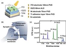
Photoelectric synaptic devices could emulate synaptic behaviors utilizing photoelectric effects and offer promising prospects with their high-speed operation and low crosstalk. In this study, we introduced a novel InGaZnO-based photoelectric memristor. Under both electrical and optical stimulation, the device successfully emulated synaptic characteristics including excitatory postsynaptic current (EPSC), paired-pulse facilitation (PPF), long-term potentiation (LTP), and long-term depression (LTD). Furthermore, we demonstrated the practical application of our synaptic devices through the recognition of handwritten digits. The devices have successfully shown their ability to modulate synaptic weights effectively through light pulse stimulation, resulting in a recognition accuracy of up to 93.4%. The results illustrated the potential of IGZO-based memristors in neuromorphic computing, particularly their ability to simulate synaptic functionalities and contribute to image recognition tasks.
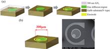
This paper examines GaSb short-wavelength infrared detectors employing planar PN junctions. The fabrication was based on the Zn diffusion process and the diffusion temperature was optimized. Characterization revealed a 50% cut-off wavelength of 1.73 μm, a maximum detectivity of 8.73 × 1010 cm·Hz1/2/W, and a minimum dark current density of 1.02 × 10?5 A/cm2. Additionally, a maximum quantum efficiency of 60.3% was achieved. Subsequent optimization of fabrication enabled the realization of a 320 × 256 focal plane array that exhibited satisfactory imaging results. Remarkably, the GaSb planar detectors demonstrated potential in low-cost short wavelength infrared imaging, without requiring material epitaxy or deposition.
The utilization of processing capabilities within the detector holds significant promise in addressing energy consumption and latency challenges. Especially in the context of dynamic motion recognition tasks, where substantial data transfers are necessitated by the generation of extensive information and the need for frame-by-frame analysis. Herein, we present a novel approach for dynamic motion recognition, leveraging a spatial-temporal in-sensor computing system rooted in multiframe integration by employing photodetector. Our approach introduced a retinomorphic MoS2 photodetector device for motion detection and analysis. The device enables the generation of informative final states, nonlinearly embedding both past and present frames. Subsequent multiply-accumulate (MAC) calculations are efficiently performed as the classifier. When evaluating our devices for target detection and direction classification, we achieved an impressive recognition accuracy of 93.5%. By eliminating the need for frame-by-frame analysis, our system not only achieves high precision but also facilitates energy-efficient in-sensor computing.
This work shows that despite a lattice mismatch of almost 20%, CdMnTe/CdTe/CdMnTe heterostructures grown directly on Si(111) have surprisingly good optical emission properties. The investigated structures were grown by molecular beam epitaxy and characterized by scanning transmission electron microscopy, macro- and micro-photoluminescence. Low temperature macro-photoluminescence experiments indicate three emission bands which depend on the CdTe layer thickness and have different confinement characteristics. Temperature measurements reveal that the lower energy emission band (at 1.48 eV) is associated to defects and bound exciton states, while the main emission at 1.61 eV has a weak 2D character and the higher energy one at 1.71 eV has a well-defined (zero-dimensional, 0D) 0D nature. Micro-photoluminescence measurements show the existence of sharp and strongly circularly polarized (up to 40%) emission lines which can be related to the presence of Mn in the heterostructure. This result opens the possibility of producing photon sources with the typical spin control of the diluted magnetic semiconductors using the low-cost silicon technology.
In this study, the effects of 1 MeV electron radiation on the D-mode GaN-based high electron mobility transistors (HEMTs) were investigated after different radiation doses. The changes in electrical properties of the device were obtained, and the related physical mechanisms were analyzed. It indicated that under the radiation dose of 5 × 1014 cm?2, the channel current cannot be completely pinched off even if the negative gate voltage was lower than the threshold voltage, and the gate leakage current increased significantly. The emission microscopy and scanning electron microscopy were used to determine the damage location. Besides, the radiation dose was adjusted ranging from 5 × 10¹² to 1 × 1014 cm?2, and we noticed that the drain?source current increased and the threshold voltage presented slightly negative shift. By calculations, it suggested that the carrier density and electron mobility gradually increased. It provided a reference for the development of device radiation reinforcement technology.
In this work, AlN films were grown using gallium (Ga) as surfactant on 4° off-axis 4H-SiC substrates via microwave plasma chemical vapor deposition (MPCVD). We have found that AlN growth rate can be greatly improved due to the catalytic effect of trimethyl-gallium (TMGa), but AlN crystal structure and composition are not affected. When the proportion of TMGa in gas phase was low, crystal quality of AlN can be improved and three-dimensional growth mode of AlN was enhanced with the increase of Ga source. When the proportion of TMGa in gas phase was high, two-dimensional growth mode of AlN was presented, with the increase of Ga source results in the deterioration of AlN crystal quality. Finally, employing a two-step growth approach, involving the initial growth of Ga-free AlN nucleation layer followed by Ga-assisted AlN growth, high quality of AlN film with flat surface was obtained and the full width at half maximum (FWHM) values of 415 nm AlN (002) and (102) planes were 465 and 597 arcsec.
This work presents a novel radio frequency (RF) narrowband Si micro-electro-mechanical systems (MEMS) filter based on capacitively transduced slotted width extensional mode (WEM) resonators. The flexibility of the plate leads to multiple modes near the target frequency. The high Q-factor resonators of around 100 000 enable narrow bandwidth filters with small size and simplified design. The 1-wavelength and 2-wavelength WEMs were first developed as a pair of coupled modes to form a passband. To reduce bandwidth, two plates are coupled with a λ-length coupling beam. The 79.69 MHz coupled plate filter (CPF) achieved a narrow bandwidth of 8.8 kHz, corresponding to a tiny 0.011%. The CPF exhibits an impressive 34.84 dB stopband rejection and 7.82 dB insertion loss with near-zero passband ripple. In summary, the RF MEMS filter presented in this work shows promising potential for application in RF transceiver front-ends.
Boron?nitrogen doped multiple resonance (BN-MR) emitters, characterized by B?N covalent bonds, offer distinctive advantages as pivotal building blocks for facile access to novel MR emitters featuring narrowband spectra and high efficiency. However, there remains a scarcity of exploration concerning synthetic methods and structural derivations to expand the library of novel BN-MR emitters. Herein, we present the synthesis of a BN-MR emitter, tCz[B?N]N, through a one-pot borylation reaction directed by the amine group, achieving an impressive yield of 94%. The emitter is decorated by incorporating two 3,6-di-t-butylcarbazole (tCz) units into a B?N covalent bond doped BN-MR parent molecule via para-C?π?D and para-N?π?D conjugations. This peripheral decoration strategy enhances the reverse intersystem crossing process and shifts the emission band towards the pure green region, peaking at 526 nm with a narrowband full-width at half maximum (FWHM) of 41 nm. Consequently, organic light emitting diodes (OLEDs) employing this emitter achieved a maximum external quantum efficiency (EQEmax) value of 27.7%, with minimal efficiency roll-off. Even at a practical luminance of 1000 cd?m?2, the device maintains a high EQE value of 24.6%.
Semiconductor quantum dots are promising candidates for preparing high-performance single photon sources. A basic requirement for this application is realizing the controlled growth of high-quality semiconductor quantum dots. Here, we report the growth of embedded GaAs1?xSbx quantum dots in GaAs nanowires by molecular-beam epitaxy. It is found that the size of the GaAs1?xSbx quantum dot can be well-defined by the GaAs nanowire. Energy dispersive spectroscopy analyses show that the antimony content x can be up to 0.36 by tuning the growth temperature. All GaAs1?xSbx quantum dots exhibit a pure zinc-blende phase. In addition, we have developed a new technology to grow GaAs passivation layers on the sidewalls of the GaAs1?xSbx quantum dots. Different from the traditional growth process of the passivation layer, GaAs passivation layers can be grown simultaneously with the growth of the embedded GaAs1?xSbx quantum dots. The spontaneous GaAs passivation layer shows a pure zinc-blende phase due to the strict epitaxial relationship between the quantum dot and the passivation layer. The successful fabrication of embedded high-quality GaAs1?xSbx quantum dots lays the foundation for the realization of GaAs1?xSbx-based single photon sources.
This paper presents a design of single photon avalanche diode (SPAD) light detection and ranging (LiDAR) sensor with 128 × 128 pixels and 128 column-parallel time-to-analog-merged-analog-to-digital converts (TA-ADCs). Unlike the conventional TAC-based SPAD LiDAR sensor, in which the TAC and ADC are separately implemented, we propose to merge the TAC and ADC by sharing their capacitors, thus avoiding the analog readout noise of TAC’s output buffer, improving the conversion rate, and reducing chip area. The reverse start-stop logic is employed to reduce the power of the TA-ADC. Fabricated in a 180 nm CMOS process, our prototype sensor exhibits a timing resolution of 25 ps, a DNL of +0.30/?0.77 LSB, an INL of +1.41/?2.20 LSB, and a total power consumption of 190 mW. A flash LiDAR system based on this sensor demonstrates the function of 2D/3D imaging with 128 × 128 resolution, 25 kHz inter-frame rate, and sub-centimeter ranging precision.
Ratiometric fluorescent detection of iron(Ⅲ) (Fe3+) offers inherent self-calibration and contactless analytic capabilities. However, realizing a dual-emission near-infrared (NIR) nanosensor with a low limit of detection (LOD) is rather challenging. In this work, we report the synthesis of water-dispersible erbium-hyperdoped silicon quantum dots (Si QDs:Er), which emit NIR light at the wavelengths of 810 and 1540 nm. A dual-emission NIR nanosensor based on water-dispersible Si QDs:Er enables ratiometric Fe3+ detection with a very low LOD (0.06 μM). The effects of pH, recyclability, and the interplay between static and dynamic quenching mechanisms for Fe3+ detection have been systematically studied. In addition, we demonstrate that the nanosensor may be used to construct a sequential logic circuit with memory functions.
Detectors were developed for detecting irradiation in the short-wavelength ultraviolet (UVC) interval using high-quality single-crystalline α-Ga2O3 films with Pt interdigital contacts. The films of α-Ga2O3 were grown on planar sapphire substrates with c-plane orientation using halide vapor phase epitaxy. The spectral dependencies of the photo to dark current ratio, responsivity, external quantum efficiency and detectivity of the structures were investigated in the wavelength interval of 200?370 nm. The maximum of photo to dark current ratio, responsivity, external quantum efficiency, and detectivity of the structures were 1.16 × 10⁴ arb. un., 30.6 A/W, 1.65 × 10⁴%, and 6.95 × 10¹⁵ Hz0.5·cm/W at a wavelength of 230 nm and an applied voltage of 1 V. The high values of photoelectric properties were due to the internal enhancement of the photoresponse associated with strong hole trapping. The α-Ga2O3 film-based UVC detectors can function in self-powered operation mode due to the built-in electric field at the Pt/α-Ga2O3 interfaces. At a wavelength of 254 nm and zero applied voltage, the structures exhibit a responsivity of 0.13 mA/W and an external quantum efficiency of 6.2 × 10?2%. The UVC detectors based on the α-Ga2O3 films demonstrate high-speed performance with a rise time of 18 ms in self-powered mode.
Silicon carbide (SiC), as a third-generation semiconductor material, possesses exceptional material properties that significantly enhance the performance of power devices. The SiC lateral double-diffused metal–oxide–semiconductor (LDMOS) power devices have undergone continuous optimization, resulting in an increase in breakdown voltage (BV) and ultra-low specific on-resistance (Ron,sp). This paper has summarized the structural optimizations and experimental progress of SiC LDMOS power devices, including the trench-gate technology, reduced surface field (RESURF) technology, doping technology, junction termination techniques and so on. The paper is aimed at enhancing the understanding of the operational mechanisms and providing guidelines for the further development of SiC LDMOS power devices.
Relationship between the hole concentration at room temperature and the Mg doping concentration in p-GaN grown by MOCVD after sufficient annealing was studied in this paper. Different annealing conditions were applied to obtain sufficient activation for p-GaN samples with different Mg doping ranges. Hole concentration, resistivity and mobility were characterized by room-temperature Hall measurements. The Mg doping concentration and the residual impurities such as H, C, O and Si were measured by secondary ion mass spectroscopy, confirming negligible compensations by the impurities. The hole concentration, resistivity and mobility data are presented as a function of Mg concentration, and are compared with literature data. The appropriate curve relating the Mg doping concentration to the hole concentration is derived using a charge neutrality equation and the ionized-acceptor-density [NA?] (cm?3) dependent ionization energy of Mg acceptor was determined as EAMg = 184 ? 2.66 × 10?5 × [NA?]1/3 meV.
Herein, a physical and mathematical model of the voltage?current characteristics of a p?n heterostructure with quantum wells (QWs) is prepared using the Sah?Noyce?Shockley (SNS) recombination mechanism to show the SNS recombination rate of the correction function of the distribution of QWs in the space charge region of diode configuration. A comparison of the model voltage?current characteristics (VCCs) with the experimental ones reveals their adequacy. The technological parameters of the structure of the VCC model are determined experimentally using a nondestructive capacitive approach for determining the impurity distribution profile in the active region of the diode structure with a profile depth resolution of up to 10 ?. The correction function in the expression of the recombination rate shows the possibility of determining the derivative of the VCCs of structures with QWs with a nonideality factor of up to 4.
The amorphous phase-change materials with spontaneous structural relaxation leads to the resistance drift with the time for phase-change neuron synaptic devices. Here, we modify the phase change properties of the conventional Ge2Sb2Te5 (GST) material by introducing an SnS phase. It is found that the resistance drift coefficient of SnS-doped GST was decreased from 0.06 to 0.01. It can be proposed that the origin originates from the precipitation of GST nanocrystals accompanied by the precipitation of SnS crystals compared to single-phase GST compound systems. We also found that the decrease in resistance drift can be attributed to the narrowed bandgap from 0.65 to 0.43 eV after SnS-doping. Thus, this study reveals the quantitative relationship between the resistance drift and the band gap and proposes a new idea for alleviating the resistance drift by composition optimization, which is of great significance for finding a promising phase change material.
Semiconductor materials exemplify humanity's unwavering pursuit of enhanced performance, efficiency, and functionality in electronic devices. From its early iterations to the advanced variants of today, this field has undergone an extraordinary evolution. As the reliability requirements of integrated circuits continue to increase, the industry is placing greater emphasis on the crystal qualities. Consequently, conducting a range of characterization tests on the crystals has become necessary. This paper will examine the correlation between crystal quality, device performance, and production yield, emphasizing the significance of crystal characterization tests and the important role of high-precision synchrotron radiation X-ray topography characterization in semiconductor analysis. Finally, we will cover the specific applications of synchrotron radiation characterization in the development of semiconductor materials.
Nanocomposite films consisting of carboxymethyl cellulose, polyethylene oxide (CMC/PEO), and anatase titanium dioxide (TO) were produced by the use of sol-gel and solution casting techniques. TiO2 nanocrystals were effectively incorporated into CMC/PEO polymers, as shown by X-ray diffraction (XRD) and attenuated total reflectance fourier transform infrared (ATR-FTIR) analysis. The roughness growth is at high levels of TO nanocrystals (TO NCs), which means increasing active sites and defects in CMC/PEO. In differential scanning calorimetry (DSC) thermograms, the change in glass transition temperature (Tg) values verifies that the polymer blend interacts with TO NCs. The increment proportions of TO NCs have a notable impact on the dielectric performances of the nanocomposites, as observed. The electrical properties of the CMC/PEO/TO nanocomposite undergo significant changes. The nanocomposite films exhibit a red alteration in the absorption edge as the concentration of TO NCs increases in the polymer blend. The decline in the energy gap is readily apparent as the weight percentage of TO NCs increases. The photoluminescence (PL) emission spectra indicate that the sites of the luminescence peak maximums show slight variation; peaks get wider, while their intensities decrease dramatically as the concentration of TO increases. These nanocomposite materials show potential for multifunctional applications including optoelectronics, antireflection coatings, photocatalysis, light emitting diodes, and solid polymer electrolytes.
Avalanche photodetectors (APDs) featuring an avalanche multiplication region are vital for reaching high sensitivity and responsivity in optical transceivers. Waveguide-coupled Ge-on-Si separate absorption, charge, and multiplication (SACM) APDs are popular due to their straightforward fabrication process, low optical propagation loss, and high detection sensitivity in optical communications. This paper introduces a lateral SACM Ge-on-Si APD on a silicon-on-insulator (SOI) wafer, featuring a 10 μm-long, 0.5 μm-wide Ge layer at 1310 nm on a standard 8-inch silicon photonics platform. The dark current measures approximately 38.6 μA at ?21 V, indicating a breakdown voltage greater than ?21 V for the device. The APDs exhibit a unit-gain responsivity of 0.5 A/W at ?10 V. At ?15 V, their responsivity reaches 2.98 and 2.91 A/W with input powers of ?10 and ?25 dBm, respectively. The device's 3-dB bandwidth is 15 GHz with an input power of ?15 dBm and a gain is 11.68. Experimental results show a peak in impedance at high bias voltages, attributed to inductor and capacitor (LC) circuit resonance, enhancing frequency response. Furthermore, 20 Gbps eye diagrams at ?21 V and ?9 dBm input power reveal signal to noise ratio (SNRs) of 5.30. This lateral SACM APD, compatible with the stand complementary metal oxide semiconductor (CMOS) process, shows that utilizing the peaking effect at low optical power increases bandwidth.
Memristors as non-volatile memory devices have gained numerous attentions owing to their advantages in storage, in-memory computing, synaptic applications, etc. In recent years, two-dimensional (2D) materials with moderate defects have been discovered to exist memristive feature. However, it is very difficult to obtain moderate defect degree in 2D materials, and studied on modulation means and mechanism becomes urgent and essential. In this work, we realized memristive feature with a bipolar switching and a configurable on/off ratio in a two-terminal MoS2 device (on/off ratio ~100), for the first time, from absent to present using laser-modulation to few-layer defect-free MoS2 (about 10 layers), and its retention time in both high resistance state and low resistance state can reach 2 × 10⁴ s. The mechanism of the laser-induced memristive feature has been cleared by dynamic Monte Carlo simulations and first-principles calculations. Furthermore, we verified the universality of the laser-modulation by investigating other 2D materials of TMDs. Our work will open a route to modulate and optimize the performance of 2D semiconductor memristive devices.
In–Ga–Zn–O (IGZO) channel based thin-film transistors (TFT), which exhibit high on–off current ratio and relatively high mobility, has been widely researched due to its back end of line (BEOL)-compatible potential for the next generation dynamic random access memory (DRAM) application. In this work, thermal atomic layer deposition (TALD) indium gallium zinc oxide (IGZO) technology was explored. It was found that the atomic composition and the physical properties of the IGZO films can be modulated by changing the sub-cycles number during atomic layer deposition (ALD) process. In addition, thin-film transistors (TFTs) with vertical channel-all-around (CAA) structure were realized to explore the influence of different IGZO films as channel layers on the performance of transistors. Our research demonstrates that TALD is crucial for high density integration technology, and the proposed vertical IGZO CAA-TFT provides a feasible path to break through the technical problems for the continuous scale of electronic equipment.
In this paper, we explore the electrical characteristics of high-electron-mobility transistors (HEMTs) using a TaN/AlGaN/GaN metal insulating semiconductor (MIS) structure. The high-resistance tantalum nitride (TaN) film prepared by magnetron sputtering as the gate dielectric layer of the device achieved an effective reduction of electronic states at the TaN/AlGaN interface, and reducing the gate leakage current of the MIS HEMT, its performance was enhanced. The HEMT exhibited a low gate leakage current of 2.15 × 10?7 mA/mm and a breakdown voltage of 1180 V. Furthermore, the MIS HEMT displayed exceptional operational stability during dynamic tests, with dynamic resistance remaining only 1.39 times even under 400 V stress.
All-dielectric metasurface, which features low optical absorptance and high resolution, is becoming a promising candidate for full-color generation. However, the optical response of current metamaterials is fixed and lacks active tuning. In this work, we demonstrate a reconfigurable and polarization-dependent active color generation technique by incorporating low-loss phase change materials (PCMs) and CaF2 all-dielectric substrate. Based on the strong Mie resonance effect and low optical absorption structure, a transflective, full-color with high color purity and gamut value is achieved. The spectrum can be dynamically manipulated by changing either the polarization of incident light or the PCM state. High transmittance and reflectance can be simultaneously achieved by using low-loss PCMs and substrate. The novel active metasurfaces can bring new inspiration in the areas of optical encryption, anti-counterfeiting, and display technologies.
Radiation damage produced in 4H-SiC by electrons of different doses is presented by using multiple characterization techniques. Raman spectra results indicate that SiC crystal structures are essentially impervious to 10 MeV electron irradiation with doses up to 3000 kGy. However, irradiation indeed leads to the generation of various defects, which are evaluated through photoluminescence (PL) and deep level transient spectroscopy (DLTS). The PL spectra feature a prominent broad band centered at 500 nm, accompanied by several smaller peaks ranging from 660 to 808 nm. The intensity of each PL peak demonstrates a linear correlation with the irradiation dose, indicating a proportional increase in defect concentration during irradiation. The DLTS spectra reveal several thermally unstable and stable defects that exhibit similarities at low irradiation doses. Notably, after irradiating at the higher dose of 1000 kGy, a new stable defect labeled as R2 (Ec ? 0.51 eV) appeared after annealing at 800 K. Furthermore, the impact of irradiation-induced defects on SiC junction barrier Schottky diodes is discussed. It is observed that high-dose electron irradiation converts SiC n-epilayers to semi-insulating layers. However, subjecting the samples to a temperature of only 800 K results in a significant reduction in resistance due to the annealing out of unstable defects.
Growth of gallium nitride (GaN) inverted pyramids on c-plane sapphire substrates is benefit for fabricating novel devices as it forms the semipolar facets. In this work, GaN inverted pyramids are directly grown on c-plane patterned sapphire substrates (PSS) by metal organic vapor phase epitaxy (MOVPE). The influences of growth conditions on the surface morphology are experimentally studied and explained by Wulff constructions. The competition of growth rate among {0001}, {101ˉ1}, and {112ˉ2} facets results in the various surface morphologies of GaN. A higher growth temperature of 985 °C and a lower Ⅴ/Ⅲ ratio of 25 can expand the area of {112ˉ2} facets in GaN inverted pyramids. On the other hand, GaN inverted pyramids with almost pure {101ˉ1} facets are obtained by using a lower growth temperature of 930 °C, a higher Ⅴ/Ⅲ ratio of 100, and PSS with pattern arrangement perpendicular to the substrate primary flat.
A 28/56 Gb/s NRZ/PAM-4 dual-mode transceiver (TRx) designed in a 28-nm complementary metal-oxide-semiconductor (CMOS) process is presented in this article. A voltage-mode (VM) driver featuring a 4-tap reconfigurable feed-forward equalizer (FFE) is employed in the quarter-rate transmitter (TX). The half-rate receiver (RX) incorporates a continuous-time linear equalizer (CTLE), a 3-stage high-speed slicer with multi-clock-phase sampling, and a clock and data recovery (CDR). The experimental results show that the TRx operates at a maximum speed of 56 Gb/s with chip-on board (COB) assembly. The 28 Gb/s NRZ eye diagram shows a far-end vertical eye opening of 210 mV with an output amplitude of 351 mV single-ended and the 56 Gb/s PAM-4 eye diagram exhibits far-end eye opening of 33 mV (upper-eye), 31 mV (mid-eye), and 28 mV (lower-eye) with an output amplitude of 353 mV single-ended. The recovered 14 GHz clock from the RX exhibits random jitter (RJ) of 469 fs and deterministic jitter (DJ) of 8.76 ps. The 875 Mb/s de-multiplexed data features 593 ps horizontal eye opening with 32.02 ps RJ, at bit-error rate (BER) of 10?5 (0.53 UI). The power dissipation of TX and RX are 125 and 181.4 mW, respectively, from a 0.9-V supply.
In this paper, an NMOS output-capacitorless low-dropout regulator (OCL-LDO) featuring dual-loop regulation has been proposed, achieving fast transient response with low power consumption. An event-driven charge pump (CP) loop with the dynamic strength control (DSC), is proposed in this paper, which overcomes trade-offs inherent in conventional structures. The presented design addresses and resolves the large signal stability issue, which has been previously overlooked in the event-driven charge pump structure. This breakthrough allows for the full exploitation of the charge-pump structure's potential, particularly in enhancing transient recovery. Moreover, a dynamic error amplifier is utilized to attain precise regulation of the steady-state output voltage, leading to favorable static characteristics. A prototype chip has been fabricated in 65 nm CMOS technology. The measurement results show that the proposed OCL-LDO achieves a 410 nA low quiescent current (IQ) and can recover within 30 ns under 200 mA/10 ns loading change.
A frequency servo system-on-chip (FS-SoC) featuring output power stabilization technology is introduced in this study for high-precision and miniaturized cesium (Cs) atomic clocks. The proposed power stabilization loop (PSL) technique, incorporating an off-chip power detector (PD), ensures that the output power of the FS-SoC remains stable, mitigating the impact of power fluctuations on the atomic clock's stability. Additionally, a one-pulse-per-second (1PPS) is employed to synchronize the clock with GPS. Fabricated using 65 nm CMOS technology, the measured phase noise of the FS-SoC stands at ?69.5 dBc/Hz@100 Hz offset and ?83.9 dBc/Hz@1 kHz offset, accompanied by a power dissipation of 19.7 mW. The Cs atomic clock employing the proposed FS-SoC and PSL obtains an Allan deviation of 1.7 × 10?11 with 1-s averaging time.
Memtransistors in which the source?drain channel conductance can be nonvolatilely manipulated through the gate signals have emerged as promising components for implementing neuromorphic computing. On the other side, it is known that the complementary metal-oxide-semiconductor (CMOS) field effect transistors have played the fundamental role in the modern integrated circuit technology. Therefore, will complementary memtransistors (CMT) also play such a role in the future neuromorphic circuits and chips? In this review, various types of materials and physical mechanisms for constructing CMT (how) are inspected with their merits and need-to-address challenges discussed. Then the unique properties (what) and potential applications of CMT in different learning algorithms/scenarios of spiking neural networks (why) are reviewed, including supervised rule, reinforcement one, dynamic vision with in-sensor computing, etc. Through exploiting the complementary structure-related novel functions, significant reduction of hardware consuming, enhancement of energy/efficiency ratio and other advantages have been gained, illustrating the alluring prospect of design technology co-optimization (DTCO) of CMT towards neuromorphic computing.
This paper presents a 16-bit, 18-MSPS (million samples per second) flash-assisted successive-approximation-register (SAR) analog-to-digital converter (ADC) utilizing hybrid synchronous and asynchronous (HYSAS) timing control logic based on an on-chip delay-locked loop (DLL). The HYSAS scheme can provide a longer settling time for the capacitive digital-to-analog converter (CDAC) than the synchronous and asynchronous SAR ADC. Therefore, the issue of incomplete settling or ringing in the DAC voltage for cases of either on-chip or off-chip reference voltage can be solved to a large extent. In addition, the foreground calibration of the CDAC’s mismatch is performed with a finite-impulse-response bandpass filter (FIR-BPF) based least-mean-square (LMS) algorithm in an off-chip FPGA (field programmable gate array). Fabricated in 40-nm CMOS process, the prototype ADC achieves 94.02-dB spurious-free dynamic range (SFDR), and 75.98-dB signal-to-noise-and-distortion ratio (SNDR) for a 2.88-MHz input under 18-MSPS sampling rate.
Robots are widely used, providing significant convenience in daily life and production. With the rapid development of artificial intelligence and neuromorphic computing in recent years, the realization of more intelligent robots through a profound intersection of neuroscience and robotics has received much attention. Neuromorphic circuits based on memristors used to construct hardware neural networks have proved to be a promising solution of shattering traditional control limitations in the field of robot control, showcasing characteristics that enhance robot intelligence, speed, and energy efficiency. Starting with introducing the working mechanism of memristors and peripheral circuit design, this review gives a comprehensive analysis on the biomimetic information processing and biomimetic driving operations achieved through the utilization of neuromorphic circuits in brain-like control. Four hardware neural network approaches, including digital-analog hybrid circuit design, novel device structure design, multi-regulation mechanism, and crossbar array, are summarized, which can well simulate the motor decision-making mechanism, multi-information integration and parallel control of brain at the hardware level. It will be definitely conductive to promote the application of memristor-based neuromorphic circuits in areas such as intelligent robotics, artificial intelligence, and neural computing. Finally, a conclusion and future prospects are discussed.
We demonstrated a scheme of phase-locked terahertz quantum cascade lasers (THz QCLs) array, with a single-mode pulse power of 108 mW at 13 K. The device utilizes a Talbot cavity to achieve phase locking among five ridge lasers with first-order buried distributed feedback (DFB) grating, resulting in nearly five times amplification of the single-mode power. Due to the optimum length of Talbot cavity depends on wavelength, the combination of Talbot cavity with the DFB grating leads to better power amplification than the combination with multimode Fabry?Perot (F?P) cavities. The Talbot cavity facet reflects light back to the ridge array direction and achieves self-imaging in the array, enabling phase-locked operation of ridges. We set the spacing between adjacent elements to be 220 μm, much larger than the free-space wavelength, ensuring the operation of the fundamental supermode throughout the laser's dynamic range and obtaining a high-brightness far-field distribution. This scheme provides a new approach for enhancing the single-mode power of THz QCLs.
Enhancement-mode (E-mode) GaN-on-Si radio-frequency (RF) high-electron-mobility transistors (HEMTs) were fabricated on an ultrathin-barrier (UTB) AlGaN (<6 nm)/GaN heterostructure featuring a naturally depleted 2-D electron gas (2DEG) channel. The fabricated E-mode HEMTs exhibit a relatively high threshold voltage (VTH) of +1.1 V with good uniformity. A maximum current/power gain cut-off frequency (fT/fMAX) of 31.3/99.6 GHz with a power added efficiency (PAE) of 52.47% and an output power density (Pout) of 1.0 W/mm at 3.5 GHz were achieved on the fabricated E-mode HEMTs with 1-μm gate and Au-free ohmic contact.
Two-dimension (2D) van der Waals heterojunction holds essential promise in achieving high-performance flexible near-infrared (NIR) photodetector. Here, we report the successful fabrication of ZnSb/Ti3C2Tx MXene based flexible NIR photodetector array via a facile photolithography technology. The single ZnSb/Ti3C2Tx photodetector exhibited a high light-to-dark current ratio of 4.98, fast response/recovery time (2.5/1.3 s) and excellent stability due to the tight connection between 2D ZnSb nanoplates and 2D Ti3C2Tx MXene nanoflakes, and the formed 2D van der Waals heterojunction. Thin polyethylene terephthalate (PET) substrate enables the ZnSb/Ti3C2Tx photodetector withstand bending such that stable photoelectrical properties with non-obvious change were maintained over 5000 bending cycles. Moreover, the ZnSb/Ti3C2Tx photodetectors were integrated into a 26 × 5 device array, realizing a NIR image sensing application.
High quality β-Ga2O3 single crystal nanobelts with length of 2?3 mm and width from tens of microns to 132 μm were synthesized by carbothermal reduction method. Based on the grown nanobelt with the length of 600 μm, the dual-Schottky-junctions coupling device (DSCD) was fabricated. Due to the electrically floating Ga2O3 nanobelt region coupling with the double Schottky-junctions, the current IS2 increases firstly and rapidly reaches into saturation as increase the voltage VS2. The saturation current is about 10 pA, which is two orders of magnitude lower than that of a single Schottky-junction. In the case of solar-blind ultraviolet (UV) light irradiation, the photogenerated electrons further aggravate the coupling physical mechanism in device. IS2 increases as the intensity of UV light increases. Under the UV light of 1820 μW/cm2, IS2 quickly enters the saturation state. At VS2 = 10 V, photo-to-dark current ratio (PDCR) of the device reaches more than 104, the external quantum efficiency (EQE) is 1.6 × 10³%, and the detectivity (D*) is 7.5 × 10¹² Jones. In addition, the device has a very short rise and decay times of 25?54 ms under different positive and negative bias. DSCD shows unique electrical and optical control characteristics, which will open a new way for the application of nanobelt-based devices.
This work reports the growth and characterization of p-AlInN layers doped with Mg by plasma-assisted molecular beam epitaxy (PAMBE). AlInN was grown with an Al molar fraction of 0.80 by metal-modulated epitaxy (MME) with a thickness of 180 nm on Si(111) substrates using AlN as buffer layers. Low substrate temperatures were used to enhance the incorporation of indium atoms into the alloy without clustering, as confirmed by X-ray diffraction (XRD). Cathodoluminescence measurements revealed ultraviolet (UV) range emissions. Meanwhile, Hall effect measurements indicated a maximum hole mobility of 146 cm2/(V?s), corresponding to a free hole concentration of 1.23 × 1019 cm?3. The samples were analyzed by X-ray photoelectron spectroscopy (XPS) estimating the alloy composition and extracting the Fermi level by valence band analysis. Mg-doped AlInN layers were studied for use as the electron-blocking layer (EBL) in LED structures. We varied the Al composition in the EBL from 0.84 to 0.96 molar fraction to assess its theoretical effects on electroluminescence, carrier concentration, and electric field, using SILVACO Atlas. The results from this study highlight the importance and capability of producing high-quality Mg-doped p-AlInN layers through PAMBE. Our simulations suggest that an Al content of 0.86 is optimal for achieving desired outcomes in electroluminescence, carrier concentration, and electric field.
Reducing the process variation is a significant concern for resistive random access memory (RRAM). Due to its ultra-high integration density, RRAM arrays are prone to lithographic variation during the lithography process, introducing electrical variation among different RRAM devices. In this work, an optical physical verification methodology for the RRAM array is developed, and the effects of different layout parameters on important electrical characteristics are systematically investigated. The results indicate that the RRAM devices can be categorized into three clusters according to their locations and lithography environments. The read resistance is more sensitive to the locations in the array (~30%) than SET/RESET voltage (<10%). The increase in the RRAM device length and the application of the optical proximity correction technique can help to reduce the variation to less than 10%, whereas it reduces RRAM read resistance by 4×, resulting in a higher power and area consumption. As such, we provide design guidelines to minimize the electrical variation of RRAM arrays due to the lithography process.
An accurate and novel small-signal equivalent circuit model for GaN high-electron-mobility transistors (HEMTs) is proposed, which considers a dual-field-plate (FP) made up of a gate-FP and a source-FP. The equivalent circuit of the overall model is composed of parasitic elements, intrinsic transistors, gate-FP, and source-FP networks. The equivalent circuit of the gate-FP is identical to that of the intrinsic transistor. In order to simplify the complexity of the model, a series combination of a resistor and a capacitor is employed to represent the source-FP. The analytical extraction procedure of the model parameters is presented based on the proposed equivalent circuit. The verification is carried out on a 4 × 250 μm GaN HEMT device with a gate-FP and a source-FP in a 0.45 μm technology. Compared with the classic model, the proposed novel small-signal model shows closer agreement with measured S-parameters in the range of 1.0 to 18.0 GHz.
There are challenges to the reliability evaluation for insulated gate bipolar transistors (IGBT) on electric vehicles, such as junction temperature measurement, computational and storage resources. In this paper, a junction temperature estimation approach based on neural network without additional cost is proposed and the lifetime calculation for IGBT using electric vehicle big data is performed. The direct current (DC) voltage, operation current, switching frequency, negative thermal coefficient thermistor (NTC) temperature and IGBT lifetime are inputs. And the junction temperature (Tj) is output. With the rain flow counting method, the classified irregular temperatures are brought into the life model for the failure cycles. The fatigue accumulation method is then used to calculate the IGBT lifetime. To solve the limited computational and storage resources of electric vehicle controllers, the operation of IGBT lifetime calculation is running on a big data platform. The lifetime is then transmitted wirelessly to electric vehicles as input for neural network. Thus the junction temperature of IGBT under long-term operating conditions can be accurately estimated. A test platform of the motor controller combined with the vehicle big data server is built for the IGBT accelerated aging test. Subsequently, the IGBT lifetime predictions are derived from the junction temperature estimation by the neural network method and the thermal network method. The experiment shows that the lifetime prediction based on a neural network with big data demonstrates a higher accuracy than that of the thermal network, which improves the reliability evaluation of system.
Electrochemical impedance spectroscopy (EIS) flow cytometry offers the advantages of speed, affordability, and portability in cell analysis and cytometry applications. However, the integration challenges of microfluidic and EIS read-out circuits hinder the downsizing of cytometry devices. To address this, we developed a thermal-bubble-driven impedance flow cytometric application-specific integrated circuit (ASIC). The thermal-bubble micropump avoids external piping and equipment, enabling high-throughput designs. With a total of 36 cell counting channels, each measuring 884 × 220 μm2, the chip significantly enhances the throughput of flow cytometers. Each cell counting channel incorporates a differential trans-impedance amplifier (TIA) to amplify weak biosensing signals. By eliminating the parasitic parameters created at the complementary metal-oxide-semiconductor transistor (CMOS)-micro-electromechanical systems (MEMS) interface, the counting accuracy can be increased. The on-chip TIA can adjust feedback resistance from 5 to 60 kΩ to accommodate solutions with different impedances. The chip effectively classifies particles of varying sizes, demonstrated by the average peak voltages of 0.0529 and 0.4510 mV for 7 and 14 μm polystyrene beads, respectively. Moreover, the counting accuracies of the chip for polystyrene beads and MSTO-211H cells are both greater than 97.6%. The chip exhibits potential for impedance flow cytometer at low cost, high-throughput, and miniaturization for the application of point-of-care diagnostics.
Two-dimensional (2D) materials have attracted tremendous interest in view of the outstanding optoelectronic properties, showing new possibilities for future photovoltaic devices toward high performance, high specific power and flexibility. In recent years, substantial works have focused on 2D photovoltaic devices, and great progress has been achieved. Here, we present the review of recent advances in 2D photovoltaic devices, focusing on 2D-material-based Schottky junctions, homojunctions, 2D?2D heterojunctions, 2D?3D heterojunctions, and bulk photovoltaic effect devices. Furthermore, advanced strategies for improving the photovoltaic performances are demonstrated in detail. Finally, conclusions and outlooks are delivered, providing a guideline for the further development of 2D photovoltaic devices.
The flexible perovskite light-emitting diodes (FPeLEDs), which can be expediently integrated to portable and wearable devices, have shown great potential in various applications. The FPeLEDs inherit the unique optical properties of metal halide perovskites, such as tunable bandgap, narrow emission linewidth, high photoluminescence quantum yield, and particularly, the soft nature of lattice. At present, substantial efforts have been made for FPeLEDs with encouraging external quantum efficiency (EQE) of 24.5%. Herein, we summarize the recent progress in FPeLEDs, focusing on the strategy developed for perovskite emission layers and flexible electrodes to facilitate the optoelectrical and mechanical performance. In addition, we present relevant applications of FPeLEDs in displays and beyond. Finally, perspective toward the future development and applications of flexible PeLEDs are also discussed.
Li2MnO3 and Li2RuO3 represent two prototype Li-rich transition metal (TM) oxides as high-capacity cathodes for Li-ion batteries, which have similar crystal structures but show quite different cycling performances. Here, based on the first-principles calculations, we systematically studied the electronic structures and defect properties of these two Li-rich cathodes, in order to get more understanding on the structural degradation mechanism in Li-rich TM oxides. Our calculations indicated that the structural and cycling stability of Li2MnO3 and Li2RuO3 depend closely on their electronic structures, especially the energy of their highest occupied electronic states (HOS), as it largely determines the defect properties of these cathodes. For Li2MnO3 with low-energy HOS, we found that, due to the defect charge transfer mechanism, various defects can form spontaneously in its host structure as Li ions are extracted upon delithiation, which seriously deteriorates its structural and cycling stability. While for Li2RuO3, on the other hand, we identified that the high-energy HOS prevents it from the defect formation upon delithiation and thus preserve its cycling reversibility. Our studies thus illustrated an electronic origin of the structural degradation in Li-rich TM oxides and implied that it is possible to improve their cycling performances by carefully adjusting their TM components.
Quantum key distribution (QKD), rooted in quantum mechanics, offers information-theoretic security. However, practical systems open security threats due to imperfections, notably bright-light blinding attacks targeting single-photon detectors. Here, we propose a concise, robust defense strategy for protecting single-photon detectors in QKD systems against blinding attacks. Our strategy uses a dual approach: detecting the bias current of the avalanche photodiode (APD) to defend against continuous-wave blinding attacks, and monitoring the avalanche amplitude to protect against pulsed blinding attacks. By integrating these two branches, the proposed solution effectively identifies and mitigates a wide range of bright light injection attempts, significantly enhancing the resilience of QKD systems against various bright-light blinding attacks. This method fortifies the safeguards of quantum communications and offers a crucial contribution to the field of quantum information security.
High-quality bonding of 4-inch GaAs and Si is achieved using plasma-activated bonding technology. The influence of Ar plasma activation on surface morphology is discussed. When the annealing temperature is 300 ℃, the bonding strength reaches a maximum of 6.2 MPa. In addition, a thermal stress model for GaAs/Si wafers is established based on finite element analysis to obtain the distribution of equivalent stress and deformation variables at different temperatures. The shape variation of the wafer is directly proportional to the annealing temperature. At an annealing temperature of 400 ℃, the maximum protrusion of 4 inches GaAs/Si wafers is 3.6 mm. The interface of GaAs/Si wafers is observed to be dense and defect-free using a transmission electron microscope. The characterization of interface elements by X-ray energy dispersion spectroscopy indicates that the elements at the interface undergo mutual diffusion, which is beneficial for improving the bonding strength of the interface. There is an amorphous transition layer with a thickness of about 5 nm at the bonding interface. The preparation of Si-based GaAs heterojunctions can enrich the types of materials required for the development of integrated circuits, improve the performance of materials and devices, and promote the development of microelectronics technology.
The high critical electric field strength of Ga2O3 enables higher operating voltages and reduced switching losses in power electronic devices. Suitable Schottky metals and epitaxial films are essential for further enhancing device performance. In this work, the fabrication of vertical Ga2O3 barrier diodes with three different barrier metals was carried out on an n–-Ga2O3 homogeneous epitaxial film deposited on an n+-β-Ga2O3 substrate by metal?organic chemical vapor deposition, excluding the use of edge terminals. The ideal factor, barrier height, specific on-resistance, and breakdown voltage characteristics of all devices were investigated at room temperature. In addition, the vertical Ga2O3 barrier diodes achieve a higher breakdown voltage and exhibit a reverse leakage as low as 4.82 ×10?8 A/cm2 by constructing a NiO/Ga2O3 heterojunction. Therefore, Ga2O3 power detailed investigations into Schottky barrier metal and NiO/Ga2O3 heterojunction of Ga2O3 homogeneous epitaxial films are of great research potential in high-efficiency, high-power, and high-reliability applications.
High-speed solar-blind short wavelength ultraviolet radiation detectors based on κ(ε)-Ga2O3 layers with Pt contacts were demonstrated and their properties were studied in detail. The κ(ε)-Ga2O3 layers were deposited by the halide vapor phase epitaxy on patterned GaN templates with sapphire substrates. The spectral dependencies of the photoelectric properties of structures were analyzed in the wavelength interval 200–370 nm. The maximum photo to dark current ratio, responsivity, detectivity and external quantum efficiency of structures were determined as: 180.86 arb. un., 3.57 A/W, 1.78 × 10¹² Hz0.5?cm?W?1 and 2193.6%, respectively, at a wavelength of 200 nm and an applied voltage of 1 V. The enhancement of the photoresponse was caused by the decrease in the Schottky barrier at the Pt/κ(ε)?Ga2O3 interface under ultraviolet exposure. The detectors demonstrated could functionalize in self-powered mode due to built-in electric field at the Pt/κ(ε)-Ga2O3 interface. The responsivity and external quantum efficiency of the structures at a wavelength of 254 nm and zero applied voltage were 0.9 mA/W and 0.46%, respectively. The rise and decay times in self-powered mode did not exceed 100 ms.
A nitrogen-polarity (N-polarity) GaN-based high electron mobility transistor (HEMT) shows great potential for high-frequency solid-state power amplifier applications because its two-dimensional electron gas (2DEG) density and mobility are minimally affected by device scaling. However, the Schottky barrier height (SBH) of N-polarity GaN is low. This leads to a large gate leakage in N-polarity GaN-based HEMTs. In this work, we investigate the effect of annealing on the electrical characteristics of N-polarity GaN-based Schottky barrier diodes (SBDs) with Ni/Au electrodes. Our results show that the annealing time and temperature have a large influence on the electrical properties of N-polarity GaN SBDs. Compared to the N-polarity SBD without annealing, the SBH and rectification ratio at ±5 V of the SBD are increased from 0.51 eV and 30 to 0.77 eV and 7700, respectively, and the ideal factor of the SBD is decreased from 1.66 to 1.54 after an optimized annealing process. Our analysis results suggest that the improvement of the electrical properties of SBDs after annealing is mainly due to the reduction of the interface state density between Schottky contact metals and N-polarity GaN and the increase of barrier height for the electron emission from the trap state at low reverse bias.
The detrimental effect of imprint, which can cause misreading problem, has hindered the application of ferroelectric HfO2. In this work, we present results of a comprehensive reliability evaluation of Hf0.5Zr0.5O2-based ferroelectric random access memory. The influence of imprint on the retention and endurance is demonstrated. Furthermore, a solution in circuity is proposed to effectively solve the misreading problem caused by imprint.
Applying pressure has been evidenced as an effective method to control the properties of semiconductors, owing to its capability to modify the band configuration around Fermi energy. Correspondingly, structural evolutions under external pressures are required to analyze the mechanisms. Herein high-pressure structure of a magnetic doped semiconductor Ba(Zn0.95Mn0.05)2As2 is studied with combination of in-situ synchrotron X-ray diffractions and diamond anvil cells. The materials become ferromagnetic with Curie temperature of 105 K after further 20% K doping. The title material undergoes an isostructural phase transition at around 19 GPa. Below the transition pressure, it is remarkable to find lengthening of Zn/Mn?As bond within Zn/MnAs layers, since chemical bonds are generally shortened with applying pressures. Accompanied with the bond stretch, interlayer As?As distances become shorter and the As?As dimers form after the phase transition. With further compression, Zn/Mn?As bond becomes shortened due to the recovery of isotropic compression on the Zn/MnAs layers.
Atomically thin MoSe2 layers, as a core member of the transition metal dichalcogenides (TMDs) family, benefit from their appealing properties, including tunable band gaps, high exciton binding energies, and giant oscillator strengths, thus providing an intriguing platform for optoelectronic applications of light-emitting diodes (LEDs), field-effect transistors (FETs), single-photon emitters (SPEs), and coherent light sources (CLSs). Moreover, these MoSe2 layers can realize strong excitonic emission in the near-infrared wavelengths, which can be combined with the silicon-based integration technologies and further encourage the development of the new generation technologies of on-chip optical interconnection, quantum computing, and quantum information processing. Herein, we overview the state-of-the-art applications of light-emitting devices based on two-dimensional MoSe2 layers. Firstly, we introduce recent developments in excitonic emission features from atomically thin MoSe2 and their dependences on typical physical fields. Next, we focus on the exciton-polaritons and plasmon-exciton polaritons in MoSe2 coupled to the diverse forms of optical microcavities. Then, we highlight the promising applications of LEDs, SPEs, and CLSs based on MoSe2 and their heterostructures. Finally, we summarize the challenges and opportunities for high-quality emission of MoSe2 and high-performance light-emitting devices.
The emergent two-dimensional (2D) material, tin diselenide (SnSe2), has garnered significant consideration for its potential in image capturing systems, optical communication, and optoelectronic memory. Nevertheless, SnSe2-based photodetection faces obstacles, including slow response speed and low normalized detectivity. In this work, photodetectors based on SnS/SnSe2 and SnSe/SnSe2 p?n heterostructures have been implemented through a polydimethylsiloxane (PDMS)?assisted transfer method. These photodetectors demonstrate broad-spectrum photoresponse within the 405 to 850 nm wavelength range. The photodetector based on the SnS/SnSe2 heterostructure exhibits a significant responsivity of 4.99 × 10³ A?W?1, normalized detectivity of 5.80 × 1012 cm?Hz1/2?W?1, and fast response time of 3.13 ms, respectively, owing to the built-in electric field. Meanwhile, the highest values of responsivity, normalized detectivity, and response time for the photodetector based on the SnSe/SnSe2 heterostructure are 5.91 × 10³ A?W?1, 7.03 × 1012 cm?Hz1/2?W?1, and 4.74 ms, respectively. And their photodetection performances transcend those of photodetectors based on individual SnSe2, SnS, SnSe, and other commonly used 2D materials. Our work has demonstrated an effective strategy to improve the performance of SnSe2-based photodetectors and paves the way for their future commercialization.
We demonstrate the photon-number resolution (PNR) capability of a 1.25 GHz gated InGaAs single-photon avalanche photodiode (APD) that is equipped with a simple, low-distortion ultra-narrowband interference circuit for the rejection of its background capacitive response. Through discriminating the avalanche current amplitude, we are able to resolve up to four detected photons in a single detection gate with a detection efficiency as high as 45%. The PNR capability is limited by the avalanche current saturation, and can be increased to five photons at a lower detection efficiency of 34%. The PNR capability, combined with high efficiency and low noise, will find applications in quantum information processing technique based on photonic qubits.
Excitons have significant impacts on the properties of semiconductors. They exhibit significantly different properties when a direct semiconductor turns in to an indirect one by doping. Huybrecht variational method is also found to influence the study of exciton ground state energy and ground state binding energy in AlxGa1?xAs semiconductor spherical quantum dots. The AlxGa1?xAs is considered to be a direct semiconductor at Al concentration below 0.45, and an indirect one at the concentration above 0.45. With regards to the former, the ground state binding energy increases and decreases with Al concentration and eigenfrequency, respectively; however, while the ground state energy increases with Al concentration, it is marginally influenced by eigenfrequency. On the other hand, considering the latter, while the ground state binding energy increases with Al concentration, it decreases with eigenfrequency; nevertheless, the ground state energy increases both with Al concentration and eigenfrequency. Hence, for the better practical performance of the semiconductors, the properties of the excitons are suggested to vary by adjusting Al concentration and eigenfrequency
Emission and capture characteristics of a deep hole trap (H1) in n-GaN Schottky barrier diodes (SBDs) have been investigated by optical deep level transient spectroscopy (ODLTS). Activation energy (Eemi) and capture cross-section (σp) of H1 are determined to be 0.75 eV and 4.67 × 10?15 cm2, respectively. Distribution of apparent trap concentration in space charge region is demonstrated. Temperature-enhanced emission process is revealed by decrease of emission time constant. Electric-field-boosted trap emission kinetics are analyzed by the Poole?Frenkel emission (PFE) model. In addition, H1 shows point defect capture properties and temperature-enhanced capture kinetics. Taking both hole capture and emission processes into account during laser beam incidence, H1 features a trap concentration of 2.67 × 1015 cm?3. The method and obtained results may facilitate understanding of minority carrier trap properties in wide bandgap semiconductor material and can be applied for device reliability assessment.
In this work, a novel one-time-programmable memory unit based on a Schottky-type p-GaN diode is proposed. During the programming process, the junction switches from a high-resistance state to a low-resistance state through Schottky junction breakdown, and the state is permanently preserved. The memory unit features a current ratio of more than 103, a read voltage window of 6 V, a programming time of less than 10?4 s, a stability of more than 108 read cycles, and a lifetime of far more than 10 years. Besides, the fabrication of the device is fully compatible with commercial Si-based GaN process platforms, which is of great significance for the realization of low-cost read-only memory in all-GaN integration.
Vertical GaN power MOSFET is a novel technology that offers great potential for power switching applications. Being still in an early development phase, vertical GaN devices are yet to be fully optimized and require careful studies to foster their development. In this work, we report on the physical insights into device performance improvements obtained during the development of vertical GaN-on-Si trench MOSFETs (TMOS’s) provided by TCAD simulations, enhancing the dependability of the adopted process optimization approaches. Specifically, two different TMOS devices are compared in terms of transfer-curve hysteresis (H) and subthreshold slope (SS), showing a ≈ 75% H reduction along with a ≈ 30% SS decrease. Simulations allow attributing the achieved improvements to a decrease in the border and interface traps, respectively. A sensitivity analysis is also carried out, allowing to quantify the additional trap density reduction required to minimize both figures of merit.
The 975 nm multimode diode lasers with high-order surface Bragg diffraction gratings have been simulated and calculated using the 2D finite difference time domain (FDTD) algorithm and the scattering matrix method (SMM). The periods and etch depth of the grating parameters have been optimized. A board area laser diode (BA-LD) with high-order diffraction gratings has been designed and fabricated. At output powers up to 10.5 W, the measured spectral width of full width at half maximum (FWHM) is less than 0.5 nm. The results demonstrate that the designed high-order surface gratings can effectively narrow the spectral width of multimode semiconductor lasers at high output power.
The performance and reliability of ferroelectric thin films at temperatures around a few Kelvin are critical for their application in cryo-electronics. In this work, TiN/Hf0.5Zr0.5O2/TiN capacitors that are free from the wake-up effect are investigated systematically from room temperature (300 K) to cryogenic temperature (30 K). We observe a consistent decrease in permittivity (εr) and a progressive increase in coercive electric field (Ec) as temperatures decrease. Our investigation reveals exceptional stability in the double remnant polarization (2Pr) of our ferroelectric thin films across a wide temperature range. Specifically, at 30 K, a 2Pr of 36 μC/cm2 under an applied electric field of 3.0 MV/cm is achieved. Moreover, we observed a reduced fatigue effect at 30 K in comparison to 300 K. The stable ferroelectric properties and endurance characteristics demonstrate the feasibility of utilizing HfO2 based ferroelectric thin films for cryo-electronics applications.
Ex situ characterization techniques in molecular beam epitaxy (MBE) have inherent limitations, such as being prone to sample contamination and unstable surfaces during sample transfer from the MBE chamber. In recent years, the need for improved accuracy and reliability in measurement has driven the increasing adoption of in situ characterization techniques. These techniques, such as reflection high-energy electron diffraction, scanning tunneling microscopy, and X-ray photoelectron spectroscopy, allow direct observation of film growth processes in real time without exposing the sample to air, hence offering insights into the growth mechanisms of epitaxial films with controlled properties. By combining multiple in situ characterization techniques with MBE, researchers can better understand film growth processes, realizing novel materials with customized properties and extensive applications. This review aims to overview the benefits and achievements of in situ characterization techniques in MBE and their applications for material science research. In addition, through further analysis of these techniques regarding their challenges and potential solutions, particularly highlighting the assistance of machine learning to correlate in situ characterization with other material information, we hope to provide a guideline for future efforts in the development of novel monitoring and control schemes for MBE growth processes with improved material properties.
The TiO2 with nanoparticles (NPs), nanowires (NWs), nanorods (NRs) and nanotubes (NTs) structures were prepared by using a in-situ hydrothermal technique, and then proposed as a photoanode for flexible dye-sensitized solar cell (FDSSC). The influences of the morphology of TiO2 on the photovoltaic performances of FDSSCs were investigated. Under rear illumination of 100 mW·cm?2, the power conversion efficiencies of FDSSCs achieved 6.96%, 7.36%, 7.65%, and 7.83% with the TiO2 photoanodes of NPs, NWs, NRs, and NTs and PEDOT counter electrode. The FDSSCs based on TiO2 NRs and NTs photoanodes have higher short circuit current densities and power conversion efficiencies than that of the others. The enhanced power conversion efficiency is responsible for their nanotubes and rod-shaped ordered structures, which are more beneficial to transmission of electron and hole in semiconductor compared to the TiO2 nanoparticles and nanowires disordered structure.
A new theoretical method to study super-multiperiod superlattices has been developed. The method combines the precision of the 8-band kp-method with the flexibility of the shooting method and the Monte Carlo approach. This method was applied to examine the finest quality samples of super-multiperiod Al0.3Ga0.7As/GaAs superlattices grown by molecular beam epitaxy. The express photoreflectance spectroscopy method was utilized to validate the proposed theoretical method. For the first time, the accurate theoretical analysis of the energy band diagram of super-multiperiod superlattices with experimental verification has been conducted. The proposed approach highly accurately determines transition peak positions and enables the calculation of the energy band diagram, transition energies, relaxation rates, and gain estimation. It has achieved a remarkably low 5% error compared to the commonly used method, which typically results in a 25% error, and allowed to recover the superlattice parameters. The retrieved intrinsic parameters of the samples aligned with XRD data and growth parameters. The proposed method also accurately predicted the escape of the second energy level for quantum well thicknesses less than 5 nm, as was observed in photoreflectance experiments. The new designs of THz light-emitting devices operating at room temperature were suggested by the developed method.
In this work, a two-step metal organic chemical vapor deposition (MOCVD) method was applied for growing β-Ga2O3 film on c-plane sapphire. Optimized buffer layer growth temperature (TB) was found at 700 °C and the β-Ga2O3 film with full width at half maximum (FWHM) of 0.66° was achieved. A metal?semiconductor?metal (MSM) solar-blind photodetector (PD) was fabricated based on the β-Ga2O3 film. Ultrahigh responsivity of 1422 A/W @ 254 nm and photo-to-dark current ratio (PDCR) of 106 at 10 V bias were obtained. The detectivity of 2.5 × 10¹⁵ Jones proved that the photodetector has outstanding performance in detecting weak signals. Moreover, the photodetector exhibited superior wavelength selectivity with rejection ratio (R250 nm/R400 nm) of 105. These results indicate that the two-step method is a promising approach for preparation of high-quality β-Ga2O3 films for high-performance solar-blind photodetectors.
A new kind of step-flow growth mode is proposed, which adopts sidewall as step source on patterned GaN substrate. The terrace width of steps originated from the sidewall was found to change with the growth temperature and ammonia flux. The growth mechanism is explained and simulated based on step motion model. This work helps better understand the behaviors of step advancement and puts forward a method of precisely modulating atomic steps.
Phase-change material (PCM) is widely used in thermal management due to their unique thermal behavior. However, related research in thermal rectifier is mainly focused on exploring the principles at the fundamental device level, which results in a gap to real applications. Here, we propose a controllable thermal rectification design towards building applications through the direct adhesion of composite thermal rectification material (TRM) based on PCM and reduced graphene oxide (rGO) aerogel to ordinary concrete walls (CWs). The design is evaluated in detail by combining experiments and finite element analysis. It is found that, TRM can regulate the temperature difference on both sides of the TRM/CWs system by thermal rectification. The difference in two directions reaches to 13.8 K at the heat flow of 80 W/m2. In addition, the larger the change of thermal conductivity before and after phase change of TRM is, the more effective it is for regulating temperature difference in two directions. The stated technology has a wide range of applications for the thermal energy control in buildings with specific temperature requirements.
We introduce a novel method to create mid-infrared (MIR) thermal emitters using fully epitaxial, metal-free structures. Through the strategic use of epsilon-near-zero (ENZ) thin films in InAs layers, we achieve a narrow-band, wide-angle, and p-polarized thermal emission spectra. This approach, employing molecular beam epitaxy, circumvents the complexities associated with current layered structures and yields temperature-resistant emission wavelengths. Our findings contribute a promising route towards simpler, more efficient MIR optoelectronic devices.
Anode materials are an essential part of lithium-ion batteries (LIBs), which determine the performance and safety of LIBs. Currently, graphite, as the anode material of commercial LIBs, is limited by its low theoretical capacity of 372 mA·h·g?1, thus hindering further development toward high-capacity and large-scale applications. Alkaline earth metal iron-based oxides are considered a promising candidate to replace graphite because of their low preparation cost, good thermal stability, superior stability, and high electrochemical performance. Nonetheless, many issues and challenges remain to be addressed. Herein, we systematically summarize the research progress of alkaline earth metal iron-based oxides as LIB anodes. Meanwhile, the material and structural properties, synthesis methods, electrochemical reaction mechanisms, and improvement strategies are introduced. Finally, existing challenges and future research directions are discussed to accelerate their practical application in commercial LIBs.
The development of semiconductors is always accompanied by the progress in controllable doping techniques. Taking AlGaN-based ultraviolet (UV) emitters as an example, despite a peak wall-plug efficiency of 15.3% at the wavelength of 275 nm, there is still a huge gap in comparison with GaN-based visible light-emitting diodes (LEDs), mainly attributed to the inefficient doping of AlGaN with increase of the Al composition. First, p-doping of Al-rich AlGaN is a long-standing challenge and the low hole concentration seriously restricts the carrier injection efficiency. Although p-GaN cladding layers are widely adopted as a compromise, the high injection barrier of holes as well as the inevitable loss of light extraction cannot be neglected. While in terms of n-doping the main issue is the degradation of the electrical property when the Al composition exceeds 80%, resulting in a low electrical efficiency in sub-250 nm UV-LEDs. This review summarizes the recent advances and outlines the major challenges in the efficient doping of Al-rich AlGaN, meanwhile the corresponding approaches pursued to overcome the doping issues are discussed in detail.
Two-dimensional (2D) WSe2 has received increasing attention due to its unique optical properties and bipolar behavior. Several WSe2-based heterojunctions exhibit bidirectional rectification characteristics, but most devices have a lower rectification ratio. In this work, the Bi2O2Se/WSe2 heterojunction prepared by us has a type Ⅱ band alignment, which can vastly suppress the channel current through the interface barrier so that the Bi2O2Se/WSe2 heterojunction device has a large rectification ratio of about 105. Meanwhile, under different gate voltage modulation, the current on/off ratio of the device changes by nearly five orders of magnitude, and the maximum current on/off ratio is expected to be achieved 106. The photocurrent measurement reveals the behavior of recombination and space charge confinement, further verifying the bidirectional rectification behavior of heterojunctions, and it also exhibits excellent performance in light response. In the future, Bi2O2Se/WSe2 heterojunction field-effect transistors have great potential to reduce the volume of integrated circuits as a bidirectional controlled switching device.
240 nm AlGaN-based micro-LEDs with different sizes are designed and fabricated. Then, the external quantum efficiency (EQE) and light extraction efficiency (LEE) are systematically investigated by comparing size and edge effects. Here, it is revealed that the peak optical output power increases by 81.83% with the size shrinking from 50.0 to 25.0 μm. Thereinto, the LEE increases by 26.21% and the LEE enhancement mainly comes from the sidewall light extraction. Most notably, transverse-magnetic (TM) mode light intensifies faster as the size shrinks due to the tilted mesa side-wall and Al reflector design. However, when it turns to 12.5 μm sized micro-LEDs, the output power is lower than 25.0 μm sized ones. The underlying mechanism is that even though protected by SiO2 passivation, the edge effect which leads to current leakage and Shockley-Read-Hall (SRH) recombination deteriorates rapidly with the size further shrinking. Moreover, the ratio of the p-contact area to mesa area is much lower, which deteriorates the p-type current spreading at the mesa edge. These findings show a role of thumb for the design of high efficiency micro-LEDs with wavelength below 250 nm, which will pave the way for wide applications of deep ultraviolet (DUV) micro-LEDs.
The InGaN films and GaN/InGaN/GaN tunnel junctions (TJs) were grown on GaN templates with plasma-assisted molecular beam epitaxy. As the In content increases, the quality of InGaN films grown on GaN templates decreases and the surface roughness of the samples increases. V-pits and trench defects were not found in the AFM images. p++-GaN/InGaN/n++-GaN TJs were investigated for various In content, InGaN thicknesses and doping concentration in the InGaN insert layer. The InGaN insert layer can promote good interband tunneling in GaN/InGaN/GaN TJ and significantly reduce operating voltage when doping is sufficiently high. The current density increases with increasing In content for the 3 nm InGaN insert layer, which is achieved by reducing the depletion zone width and the height of the potential barrier. At a forward current density of 500 A/cm2, the measured voltage was 4.31 V and the differential resistance was measured to be 3.75 × 10?3 Ω·cm2 for the device with a 3 nm p++-In0.35Ga0.65N insert layer. When the thickness of the In0.35Ga0.65N layer is closer to the “balanced” thickness, the TJ current density is higher. If the thickness is too high or too low, the width of the depletion zone will increase and the current density will decrease. The undoped InGaN layer has a better performance than n-type doping in the TJ. Polarization-engineered tunnel junctions can enhance the functionality and performance of electronic and optoelectronic devices.
Molten-alkali etching has been widely used to reveal dislocations in 4H silicon carbide (4H-SiC), which has promoted the identification and statistics of dislocation density in 4H-SiC single crystals. However, the etching mechanism of 4H-SiC is limited misunderstood. In this letter, we reveal the anisotropic etching mechanism of the Si face and C face of 4H-SiC by combining molten-KOH etching, X-ray photoelectron spectroscopy (XPS) and first-principles investigations. The activation energies for the molten-KOH etching of the C face and Si face of 4H-SiC are calculated to be 25.09 and 35.75 kcal/mol, respectively. The molten-KOH etching rate of the C face is higher than the Si face. Combining XPS analysis and first-principles calculations, we find that the molten-KOH etching of 4H-SiC is proceeded by the cycling of the oxidation of 4H-SiC by the dissolved oxygen and the removal of oxides by molten KOH. The faster etching rate of the C face is caused by the fact that the oxides on the C face are unstable, and easier to be removed with molten alkali, rather than the C face being easier to be oxidized.
In this letter, high power density AlGaN/GaN high electron-mobility transistors (HEMTs) on a freestanding GaN substrate are reported. An asymmetric Γ-shaped 500-nm gate with a field plate of 650 nm is introduced to improve microwave power performance. The breakdown voltage (BV) is increased to more than 200 V for the fabricated device with gate-to-source and gate-to-drain distances of 1.08 and 2.92 μm. A record continuous-wave power density of 11.2 W/mm@10 GHz is realized with a drain bias of 70 V. The maximum oscillation frequency (fmax) and unity current gain cut-off frequency (ft) of the AlGaN/GaN HEMTs exceed 30 and 20 GHz, respectively. The results demonstrate the potential of AlGaN/GaN HEMTs on free-standing GaN substrates for microwave power applications.
With the rapid development of machine learning, the demand for high-efficient computing becomes more and more urgent. To break the bottleneck of the traditional Von Neumann architecture, computing-in-memory (CIM) has attracted increasing attention in recent years. In this work, to provide a feasible CIM solution for the large-scale neural networks (NN) requiring continuous weight updating in online training, a flash-based computing-in-memory with high endurance (109 cycles) and ultra-fast programming speed is investigated. On the one hand, the proposed programming scheme of channel hot electron injection (CHEI) and hot hole injection (HHI) demonstrate high linearity, symmetric potentiation, and a depression process, which help to improve the training speed and accuracy. On the other hand, the low-damage programming scheme and memory window (MW) optimizations can suppress cell degradation effectively with improved computing accuracy. Even after 109 cycles, the leakage current (Ioff) of cells remains sub-10pA, ensuring the large-scale computing ability of memory. Further characterizations are done on read disturb to demonstrate its robust reliabilities. By processing CIFAR-10 tasks, it is evident that ~90% accuracy can be achieved after 109 cycles in both ResNet50 and VGG16 NN. Our results suggest that flash-based CIM has great potential to overcome the limitations of traditional Von Neumann architectures and enable high-performance NN online training, which pave the way for further development of artificial intelligence (AI) accelerators.
This article presents an 8-element dual-polarized phased-array transceiver (TRX) front-end IC for millimeter-wave (mm-Wave) 5G new radio (NR). Power enhancement technologies for power amplifiers (PA) in mm-Wave 5G phased-array TRX are discussed. A four-stage wideband high-power class-AB PA with distributed-active-transformer (DAT) power combining and multi-stage second-harmonic traps is proposed, ensuring the mitigated amplitude-to-phase (AM-PM) distortions across wide carrier frequencies without degrading transmitting (TX) power, gain and efficiency. TX and receiving (RX) switching is achieved by a matching network co-designed on-chip T/R switch. In each TRX element, 6-bit 360° phase shifting and 6-bit 31.5-dB gain tuning are respectively achieved by the digital-controlled vector-modulated phase shifter (VMPS) and differential attenuator (ATT). Fabricated in 65-nm bulk complementary metal oxide semiconductor (CMOS), the proposed TRX demonstrates the measured peak TX/RX gains of 25.5/21.3 dB, covering the 24?29.5 GHz band. The measured peak TX OP1dB and power-added efficiency (PAE) are 20.8 dBm and 21.1%, respectively. The measured minimum RX NF is 4.1 dB. The TRX achieves an output power of 11.0?12.4 dBm and error vector magnitude (EVM) of 5% with 400-MHz 5G NR FR2 OFDM 64-QAM signals across 24?29.5 GHz, covering 3GPP 5G NR FR2 operating bands of n257, n258, and n261.
(Ga,Fe)Sb is a promising magnetic semiconductor (MS) for spintronic applications because its Curie temperature (TC) is above 300 K when the Fe concentration is higher than 20%. However, the anisotropy constant Ku of (Ga,Fe)Sb is below 7.6 × 10³ erg/cm3 when Fe concentration is lower than 30%, which is one order of magnitude lower than that of (Ga,Mn)As. To address this issue, we grew Ga1-x-yFexNiySb films with almost the same x (≈24%) and different y to characterize their magnetic and electrical transport properties. We found that the magnetic anisotropy of Ga0.76-yFe0.24NiySb can be enhanced by increasing y, in which Ku is negligible at y = 1.7% but increases to 3.8 × 10⁵ erg/cm3 at y = 6.1% (TC = 354 K). In addition, the hole mobility (μ) of Ga1-x-yFexNiySb reaches 31.3 cm2/(V?s) at x = 23.7%, y = 1.7% (TC = 319 K), which is much higher than the mobility of Ga1-xFexSb at x = 25.2% (μ = 6.2 cm2/(V?s)). Our results provide useful information for enhancing the magnetic anisotropy and hole mobility of (Ga,Fe)Sb by using Ni co-doping.
In the past few years, many groups have focused on the research and development of GaN-based ultraviolet laser diodes (UV LDs). Great progresses have been achieved even though many challenges exist. In this article, we analyze the challenges of developing GaN-based ultraviolet laser diodes, and the approaches to improve the performance of ultraviolet laser diode are reviewed. With these techniques, room temperature (RT) pulsed oscillation of AlGaN UVA (ultraviolet A) LD has been realized, with a lasing wavelength of 357.9 nm. Combining with the suppression of thermal effect, the high output power of 3.8 W UV LD with a lasing wavelength of 386.5 nm was also fabricated.
The anisotropic absorption and emission from semiconductor CdSe/CdS quantum rods (QRs) provide extra benefits among other photoluminescence nanocrystals. Using photo-induced alignment technique, the QRs can be oriented in liquid crystal polymer matrix at a large scale. In this article, a 2D Dammann grating pattern, within “SKL” characters domains aligned QRs in composite film, was fabricated by multi-step photo exposure using several photo masks, and a continuous geometric lens profile pattern aligned QRs was realized by the single step polarization converting holographic irradiation method. Both polarized optical microscope and fluorescence microscope are employed to determine the liquid crystal director profiles and QRs anisotropic excitation properties. We have been able to orient the QRs in fine binary and continuous patterns that confirms the strong quantum rod aligning ability of the proposed method. Thus, the proposed approach paves a way for photo-induced flexible QRs alignments to provide a highly specific and difficult-to-replicate security application at a large scale.
The high-density, vertically aligned retinal neuron array provides effective vision, a feature we aim to replicate with electronic devices. However, the conventional complementary metal-oxide-semiconductor (CMOS) image sensor, based on separate designs for sensing, memory, and processing units, limits its integration density. Moreover, redundant signal communication significantly increases energy consumption. Current neuromorphic devices integrating sensing and signal processing show promise in various computer vision applications, but there is still a need for frame-based imaging with good compatibility. In this study, we developed a dual-mode image sensor based on a high-density all-inorganic perovskite nanowire array. The device can switch between frame-based standard imaging mode and neuromorphic imaging mode by applying different biases. This unique bias-dependent photo response is based on a well-designed energy band diagram. The biomimetic alignment of nanowires ensures the potential for high-resolution imaging. To further demonstrate the imaging ability, we conducted pattern reconstruction in both modes with a 10 × 10 crossbar device. This study introduces a novel image sensor with high compatibility and efficiency, suitable for various applications including computer vision, surveillance, and robotics.
The performance of inverted quantum-dot light-emitting diodes (QLEDs) based on solution-processed hole transport layers (HTLs) has been limited by the solvent-induced damage to the quantum dot (QD) layer during the spin-coating of the HTL. The lack of compatibility between the HTL's solvent and the QD layer results in an uneven surface, which negatively impacts the overall device performance. In this work, we develop a novel method to solve this problem by modifying the QD film with 1,8-diaminooctane to improve the resistance of the QD layer for the HTL’s solvent. The uniform QD layer leads the inverted red QLED device to achieve a low turn-on voltage of 1.8 V, a high maximum luminance of 105 500 cd/m2, and a remarkable maximum external quantum efficiency of 13.34%. This approach releases the considerable potential of HTL materials selection and offers a promising avenue for the development of high-performance inverted QLEDs.
Close-space sublimation (CSS) has been demonstrated as an alternative vacuum deposition technique for fabricating organic light-emitting diodes (OLEDs). CSS utilizes a planar donor plate pre-coated with organic thin films as an area source to rapidly transfer the donor film to a device substrate at temperatures below 200 °C. CSS is also conformal and capable of depositing on odd-shaped substrates using flexible donor media. The evaporation behaviors of organic donor films under CSS were fully characterized using model OLED materials and CSS-deposited films exhibited comparable device performances in an OLED stack to films deposited by conventional point sources. The low temperature and conformal nature of CSS, along with its high material utilization and short process time, make it a promising method for fabricating flexible OLED displays.
As growing applications demand higher driving currents of oxide semiconductor thin-film transistors (TFTs), severe instabilities and even hard breakdown under high-current stress (HCS) become critical challenges. In this work, the triggering voltage of HCS-induced self-heating (SH) degradation is defined in the output characteristics of amorphous indium-gallium-zinc oxide (a-IGZO) TFTs, and used to quantitatively evaluate the thermal generation process of channel donor defects. The fluorinated a-IGZO (a-IGZO:F) was adopted to effectively retard the triggering of the self-heating (SH) effect, and was supposed to originate from the less population of initial deep-state defects and a slower rate of thermal defect transition in a-IGZO:F. The proposed scheme noticeably enhances the high-current applications of oxide TFTs.
β-Ga2O3 Schottky barrier diodes have undergone rapid progress in research and development for power electronic applications. This paper reviews state-of-the-art β-Ga2O3 rectifier technologies, including advanced diode architectures that have enabled lower reverse leakage current via the reduced-surface-field effect. Characteristic device properties including on-resistance, breakdown voltage, rectification ratio, dynamic switching, and nonideal effects are summarized for the different devices. Notable results on the high-temperature resilience of β-Ga2O3 Schottky diodes, together with the enabling thermal packaging solutions, are also presented.
Organic-inorganic halides perovskites (OHPs) have drawn the attention of many researchers owing to their astonishing and unique optoelectronic properties. They have been extensively used for photovoltaic applications, achieving higher than 26% power conversion efficiency to date. These materials have potential to be deployed for many other applications beyond photovoltaics like photodetectors, sensors, light-emitting diodes (LEDs), and resistors. To address the looming challenge of Moore's law and the Von Neumann bottleneck, many new technologies regarding the computation of architectures and storage of information are being extensively researched. Since the discovery of the memristor as a fourth component of the circuit, many materials are explored for memristive applications. Lately, researchers have advanced the exploration of OHPs for memristive applications. These materials possess promising memristive properties and various kinds of halide perovskites have been used for different applications that are not only limited to data storage but expand towards artificial synapses, and neuromorphic computing. Herein we summarize the recent advancements of OHPs for memristive applications, their unique electronic properties, fabrication of materials, and current progress in this field with some future perspectives and outlooks.
Impedance spectroscopy has been increasingly employed in quantum dot light-emitting diodes (QLEDs) to investigate the charge dynamics and device physics. In this review, we introduce the mathematical basics of impedance spectroscopy that applied to QLEDs. In particular, we focus on the Nyquist plot, Mott−Schottky analysis, capacitance-frequency and capacitance-voltage characteristics, and the dC/dV measurement of the QLEDs. These impedance measurements can provide critical information on electrical parameters such as equivalent circuit models, characteristic time constants, charge injection and recombination points, and trap distribution of the QLEDs. However, this paper will also discuss the disadvantages and limitations of these measurements. Fundamentally, this review provides a deeper understanding of the device physics of QLEDs through the application of impedance spectroscopy, offering valuable insights into the analysis of performance loss and degradation mechanisms of QLEDs.
Indium-tin-zinc oxide (ITZO) thin-film transistor (TFT) technology holds promise for achieving high mobility and offers significant opportunities for commercialization. This paper provides a review of progress made in improving the mobility of ITZO TFTs. This paper begins by describing the development and current status of metal-oxide TFTs, and then goes on to explain the advantages of selecting ITZO as the TFT channel layer. The evaluation criteria for TFTs are subsequently introduced, and the reasons and significance of enhancing mobility are clarified. This paper then explores the development of high-mobility ITZO TFTs from five perspectives: active layer optimization, gate dielectric optimization, electrode optimization, interface optimization, and device structure optimization. Finally, a summary and outlook of the research field are presented.
Here we review two 300 °C metal–oxide (MO) thin-film transistor (TFT) technologies for the implementation of flexible electronic circuits and systems. Fluorination-enhanced TFTs for suppressing the variation and shift of turn-on voltage (VON), and dual-gate TFTs for acquiring sensor signals and modulating VON have been deployed to improve the robustness and performance of the systems in which they are deployed. Digital circuit building blocks based on fluorinated TFTs have been designed, fabricated, and characterized, which demonstrate the utility of the proposed low-temperature TFT technologies for implementing flexible electronic systems. The construction and characterization of an analog front-end system for the acquisition of bio-potential signals and an active-matrix sensor array for the acquisition of tactile images have been reported recently.
Interaction between photons and phonons in cavity optomechanical systems provides a new toolbox for quantum information technologies. A GaAs/AlAs pillar multi-optical mode microcavity optomechanical structure can obtain phonons with ultra-high frequency (~THz). However, the optical field cannot be effectively restricted when the diameter of the GaAs/AlAs pillar microcavity decreases below the diffraction limit of light. Here, we design a system that combines Ag nanocavity with GaAs/AlAs phononic superlattices, where phonons with the frequency of 4.2 THz can be confined in a pillar with ~4 nm diameter. The Qc/V reaches 0.22 nm?3, which is ~80 times that of the photonic crystal (PhC) nanobeam and ~100 times that of the hybrid point-defect PhC bowtie plasmonic nanocavity, where Qc is optical quality factor and V is mode volume. The optomechanical single-photon coupling strength can reach 12 MHz, which is an order of magnitude larger than that of the PhC nanobeam. In addition, the mechanical zero-point fluctuation amplitude is 85 fm and the efficient mass is 0.27 zg, which is much smaller than the PhC nanobeam. The phononic superlattice-Ag nanocavity optomechanical devices hold great potential for applications in the field of integrated quantum optomechanics, quantum information, and terahertz-light transducer.
A physics-based analytical expression that predicts the charge, electrical field and potential distributions along the gated region of the GaN HEMT channel has been developed. Unlike the gradual channel approximation (GCA), the proposed model considers the non-uniform variation of the concentration under the gated region as a function of terminal applied voltages. In addition, the model can capture the influence of mobility and channel temperature on the charge distribution trend. The comparison with the hydrodynamic (HD) numerical simulation showed a high agreement of the proposed model with numerical data for different bias conditions considering the self-heating and quantization of the electron concentration. The analytical nature of the model allows us to reduce the computational and time cost of the simulation. Also, it can be used as a core expression to develop a complete physics-based transistor Ⅳ model without GCA limitation.
In this work, the GaN p-MISFET with LPCVD-SiNx is studied as a gate dielectric to improve device performance. By changing the Si/N stoichiometry of SiNx, it is found that the channel hole mobility can be effectively enhanced with Si-rich SiNx gate dielectric, which leads to a respectably improved drive current of GaN p-FET. The record high channel mobility of 19.4 cm2/(V?s) was achieved in the device featuring an Enhancement-mode channel. Benefiting from the significantly improved channel mobility, the fabricated E-mode GaN p-MISFET is capable of delivering a decent-high current of 1.6 mA/mm, while simultaneously featuring a negative threshold-voltage (VTH) of –2.3 V (defining at a stringent criteria of 10 μA/mm). The device also exhibits a well pinch-off at 0 V with low leakage current of 1 nA/mm. This suggests that a decent E-mode operation of the fabricated p-FET is obtained. In addition, the VTH shows excellent stability, while the threshold-voltage hysteresis ΔVTH is as small as 0.1 V for a gate voltage swing up to –10 V, which is among the best results reported in the literature. The results indicate that optimizing the Si/N stoichiometry of LPCVD-SiNx is a promising approach to improve the device performance of GaN p-MISFET.
In this work, we developed a simple and direct circuit model with a dual two-diode model that can be solved by a SPICE numerical simulation to comprehensively describe the monolithic perovskite/crystalline silicon (PVS/c-Si) tandem solar cells. We are able to reveal the effects of different efficiency-loss mechanisms based on the illuminated current density-voltage (J-V), semi-log dark J-V, and local ideality factor (m-V) curves. The effects of the individual efficiency-loss mechanism on the tandem cell’s efficiency are discussed, including the exp(V/VT) and exp(V/2VT) recombination, the whole cell’s and subcell’s shunts, and the Ohmic-contact or Schottky-contact of the intermediate junction. We can also fit a practical J-V curve and find a specific group of parameters by the trial-and-error method. Although the fitted parameters are not a unique solution, they are valuable clues for identifying the efficiency loss with the aid of the cell’s structure and experimental processes. This method can also serve as an open platform for analyzing other tandem solar cells by substituting the corresponding circuit models. In summary, we developed a simple and effective methodology to diagnose the efficiency-loss source of a monolithic PVS/c-Si tandem cell, which is helpful to researchers who wish to adopt the proper approaches to improve their solar cells.
Antimony selenide (Sb2Se3) is an emerging solar cell material. Here, we demonstrate that an organic small molecule of 4, 4', 4''-tris(carbazol-9-yl)-triphenylamine (TCTA) can efficiently passivate the anode interface of the Sb2Se3 solar cell. We fabricated the device by the vacuum thermal evaporation, and took ITO/TCTA (3.0 nm)/Sb2Se3 (50 nm)/C60 (5.0 nm)/Alq3 (3.0 nm)/Al as the device architecture, where Alq3 is the tris(8-hydroxyquinolinato) aluminum. By introducing a TCTA layer, the open-circuit voltage is raised from 0.36 to 0.42 V, and the power conversion efficiency is significantly improved from 3.2% to 4.3%. The TCTA layer not only inhibits the chemical reaction between the ITO and Sb2Se3 during the annealing process but it also blocks the electron diffusion from Sb2Se3 to ITO anode. The enhanced performance is mainly attributed to the suppression of the charge recombination at the anode interface.
Spin injection and detection in bulk GaN were investigated by performing magnetotransport measurements at low temperatures. A non-local four-terminal lateral spin valve device was fabricated with Co/GaN Schottky contacts. The spin injection efficiency of 21% was achieved at 1.7 K. It was confirmed that the thin Schottky barrier formed between the heavily n-doped GaN and Co was conducive to the direct spin tunneling, by reducing the spin scattering relaxation through the interface states.
The stability of organic solar cells (OSCs) remains a major concern for their ultimate industrialization due to the photo, oxygen, and water susceptibility of organic photoactive materials. Usually, antioxidant additives are blended as radical scavengers into the active layer. However, it will induce the intrinsic morphology instability and adversely affect the efficiency and long-term stability. Herein, the antioxidant dibutylhydroxytoluene (BHT) group has been covalently linked onto the side chain of benzothiadiazole (BT) unit, and a series of ternary copolymers D18-Cl-BTBHTx (x = 0, 0.05, 0.1, 0.2) with varied ratio of BHT-containing side chains have been synthesized. It was found that the introduction of BHT side chains would have a negligible effect on the photophysical properties and electronic levels, and the D18-Cl-BTBHT0.05: Y6-based OSC achieved the highest power conversion efficiency (PCE) of 17.6%, which is higher than those based active layer blended with BHT additives. More importantly, the unencapsulated device based on D18-Cl-BTBHTx (x = 0.05, 0.1, 0.2) retained approximately 50% of the initial PCE over 30 hours operation under ambient conditions, significantly outperforming the control device based on D18-Cl (90% degradation in PCE after 30 h). This work provides a new structural design strategy of copolymers for OSCs with simultaneously improved efficiency and stability.
Recently, the two-dimensional (2D) form of Ruddlesden-Popper perovskite (RPP) has been widely studied. However, the synthesis of one-dimensional (1D) RPP is rarely reported. Here, we fabricated a photodetector based on RPP microwires (RPP-MWs) and compared it with a 2D-RPP photodetector. The results show that the RPP-MWs photodetector possesses a wider photoresponse range and higher responsivities of 233 A/W in the visible band and 30 A/W in the near-infrared (NIR) band. The analyses show that the synthesized RPP-MWs have a multi-layer, heterogeneous core-shell structure. This structure gives RPP-MWs a unique band structure, as well as abundant trap states and defect levels, which enable them to acquire better photoresponse performance. This configuration of RPP-MWs provides a new idea for the design and application of novel heterostructures.
Two-dimensional transition metal dichalcogenides (TMDs) have intriguing physic properties and offer an exciting platform to explore many features that are important for future devices. In this work, we synthesized monolayer WS2 as an example to study the optical response with hydrostatic pressure. The Raman results show a continuous tuning of the lattice vibrations that is induced by hydrostatic pressure. We further demonstrate an efficient pressure-induced change of the band structure and carrier dynamics via transient absorption measurements. We found that two time constants can be attributed to the capture process of two kinds of defect states, with the pressure increasing from 0.55 GPa to 2.91 GPa, both of capture processes were accelerated, and there is an inflection point within the pressure range of 1.56 GPa to 1.89 GPa. Our findings provide valuable information for the design of future optoelectronic devices.
Developing low-cost, efficient, and stable photocatalysts is one of the most promising methods for large-scale solar water splitting. As a metal-free semiconductor material with suitable band gap, graphitic carbon nitride (g-C3N4) has attracted attention in the field of photocatalysis, which is mainly attributed to its fascinating physicochemical and photoelectronic properties. However, several inherent limitations and shortcomings—involving high recombination rate of photocarriers, insufficient reaction kinetics, and optical absorption—impede the practical applicability of g-C3N4. As an effective strategy, vacancy defect engineering has been widely used for breaking through the current limitations, considering its ability to optimize the electronic structure and surface morphology of g-C3N4 to obtain the desired photocatalytic activity. This review summarizes the recent progress of vacancy defect engineered g-C3N4 for solar water splitting. The fundamentals of solar water splitting with g-C3N4 are discussed first. We then focus on the fabrication strategies and effect of vacancy generated in g-C3N4. The advances of vacancy-modified g-C3N4 photocatalysts toward solar water splitting are discussed next. Finally, the current challenges and future opportunities of vacancy-modified g-C3N4 are summarized. This review aims to provide a theoretical basis and guidance for future research on the design and development of highly efficient defective g-C3N4.
In the era of accelerated development in artificial intelligence as well as explosive growth of information and data throughput, underlying hardware devices that can integrate perception and memory while simultaneously offering the benefits of low power consumption and high transmission rates are particularly valuable. Neuromorphic devices inspired by the human brain are considered to be one of the most promising successors to the efficient in-sensory process. In this paper, a homojunction-based multi-functional optoelectronic synapse (MFOS) is proposed and testified. It enables a series of basic electrical synaptic plasticity, including paired-pulse facilitation/depression (PPF/PPD) and long-term promotion/depression (LTP/LTD). In addition, the synaptic behaviors induced by electrical signals could be instead achieved through optical signals, where its sensitivity to optical frequency allows the MFOS to simulate high-pass filtering applications in situ and the perception capability integrated into memory endows it with the information acquisition and processing functions as a visual system. Meanwhile, the MFOS exhibits its performances of associative learning and logic gates following the illumination with two different wavelengths. As a result, the proposed MFOS offers a solution for the realization of intelligent visual system and bionic electronic eye, and will provide more diverse application scenarios for future neuromorphic computing.
Gallium oxide (Ga2O3) based flexible heterojunction type deep ultraviolet (UV) photodetectors show excellent solar-blind photoelectric performance, even when not powered, which makes them ideal for use in intelligent wearable devices. However, traditional flexible photodetectors are prone to damage during use due to poor toughness, which reduces the service life of these devices. Self-healing hydrogels have been demonstrated to have the ability to repair damage and their combination with Ga2O3 could potentially improve the lifetime of the flexible photodetectors while maintaining their performance. Herein, a novel self-healing and self-powered flexible photodetector has been constructed onto the hydrogel substrate, which exhibits an excellent responsivity of 0.24 mA/W under 254 nm UV light at zero bias due to the built-in electric field originating from the PEDOT: PSS/Ga2O3 heterojunction. The self-healing of the Ga2O3 based photodetector was enabled by the reversible property of the synthesis of agarose and polyvinyl alcohol double network, which allows the photodetector to recover its original configuration and function after damage. After self-healing, the photocurrent of the photodetector decreases from 1.23 to 1.21 μA, while the dark current rises from 0.95 to 0.97 μA, with a barely unchanged of photoresponse speed. Such a remarkable recovery capability and the photodetector’s superior photoelectric performance not only significantly enhance a device lifespan but also present new possibilities to develop wearable and intelligent electronics in the future.
In this work, we reported a high-performance-based ultraviolet-visible (UV-VIS) photodetector based on a TiO2@GaOxNy-Ag heterostructure. Ag particles were introduced into TiO2@GaOxNy to enhance the visible light detection performance of the heterojunction device. At 380 nm, the responsivity and detectivity of TiO2@GaOxNy-Ag were 0.94 A/W and 4.79 × 10⁹ Jones, respectively, and they increased to 2.86 A/W and 7.96 × 10¹⁰ Jones at 580 nm. The rise and fall times of the response were 0.19/0.23 and 0.50/0.57 s, respectively. Uniquely, at 580 nm, the responsivity of fabricated devices is one to four orders of magnitude higher than that of the photodetectors based on TiO2, Ga2O3, and other heterojunctions. The excellent optoelectronic characteristics of the TiO2@GaOxNy-Ag heterojunction device could be mainly attributed to the synergistic effect of the type-Ⅱ band structure of the metal–semiconductor–metal heterojunction and the plasmon resonance effect of Ag, which not only effectively promotes the separation of photogenerated carriers but also reduces the recombination rate. It is further illuminated by finite difference time domain method (FDTD) simulation and photoelectric measurements. The TiO2@GaOxNy-Ag arrays with high-efficiency detection are suitable candidates for applications in energy-saving communication, imaging, and sensing networks.
We demonstrate superb large-area vertical β-Ga2O3 SBDs with a Schottky contact area of 1 × 1 mm2 and obtain a high-efficiency DC–DC converter based on the device. The β-Ga2O3 SBD can obtain a forward current of 8 A with a forward voltage of 5 V, and has a reverse breakdown voltage of 612 V. The forward turn-on voltage (VF) and the on-resistance (Ron) are 1.17 V and 0.46 Ω, respectively. The conversion efficiency of the β-Ga2O3 SBD-based DC–DC converter is 95.81%. This work indicates the great potential of Ga2O3 SBDs and relevant circuits in power electronic applications.
The self-heating effect severely limits device performance and reliability. Although some studies have revealed the heat distribution of β-Ga2O3 MOSFETs under biases, those devices all have small areas and have difficulty reflecting practical conditions. This work demonstrated a multi-finger β-Ga2O3 MOSFET with a maximum drain current of 0.5 A. Electrical characteristics were measured, and the heat dissipation of the device was investigated through infrared images. The relationship between device temperature and time/bias is analyzed.
A NiO/β-Ga2O3 heterojunction-gate field effect transistor (HJ-FET) is fabricated and its instability mechanisms are experimentally investigated under different gate stress voltage (VG,s) and stress times (ts). Two different degradation mechanisms of the devices under negative bias stress (NBS) are identified. At low VG,s for a short ts, NiO bulk traps trapping/de-trapping electrons are responsible for decrease/recovery of the leakage current, respectively. At higher VG,s or long ts, the device transfer characteristic curves and threshold voltage (VTH) are almost permanently negatively shifted. This is because the interface dipoles are almost permanently ionized and neutralize the ionized charges in the space charge region (SCR) across the heterojunction interface, resulting in a narrowing SCR. This provides an important theoretical guide to study the reliability of NiO/β-Ga2O3 heterojunction devices in power electronic applications.
This work demonstrates high-performance NiO/β-Ga2O3 vertical heterojunction diodes (HJDs) with double-layer junction termination extension (DL-JTE) consisting of two p-typed NiO layers with varied lengths. The bottom 60-nm p-NiO layer fully covers the β-Ga2O3 wafer, while the geometry of the upper 60-nm p-NiO layer is 10 μm larger than the square anode electrode. Compared with a single-layer JTE, the electric field concentration is inhibited by double-layer JTE structure effectively, resulting in the breakdown voltage being improved from 2020 to 2830 V. Moreover, double p-typed NiO layers allow more holes into the Ga2O3 drift layer to reduce drift resistance. The specific on-resistance is reduced from 1.93 to 1.34 mΩ·cm2. The device with DL-JTE shows a power figure-of-merit (PFOM) of 5.98 GW/cm2, which is 2.8 times larger than that of the conventional single-layer JTE structure. These results indicate that the double-layer JTE structure provides a viable way of fabricating high-performance Ga2O3 HJDs.
In this work, W/β-Ga2O3 Schottky barrier diodes, prepared using a confined magnetic field-based sputtering method, were analyzed at different operation temperatures. Firstly, Schottky barrier height increased with increasing temperature from 100 to 300 K and reached 1.03 eV at room temperature. The ideality factor decreased with increasing temperature and it was higher than 2 at 100 K. This apparent high value was related to the tunneling effect. Secondly, the series and on-resistances decreased with increasing operation temperature. Finally, the interfacial dislocation was extracted from the tunneling current. A high dislocation density was found, which indicates the domination of tunneling through dislocation in the transport mechanism. These findings are evidently helpful in designing better performance devices.
The anisotropic properties and applications of β-gallium oxide (β-Ga2O3) are comprehensively reviewed. All the anisotropic properties are essentially resulted from the anisotropic crystal structure. The process flow of how to exfoliate nanoflakes from bulk material is introduced. Anisotropic optical properties, including optical bandgap, Raman and photoluminescence characters are comprehensively reviewed. Three measurement configurations of angle-resolved polarized Raman spectra (ARPRS) are reviewed, with Raman intensity formulas calculated with Raman tensor elements. The method to obtain the Raman tensor elements of phonon modes through experimental fitting is also introduced. In addition, the anisotropy in electron mobility and affinity are discussed. The applications, especially polarization photodetectors, based on β-Ga2O3 were summarized comprehensively. Three kinds of polarization detection mechanisms based on material dichroism, 1D morphology and metal-grids are discussed in-depth. This review paper provides a framework for anisotropic optical and electric properties of β-Ga2O3, as well as the applications based on these characters, and is expected to lead to a wider discussion on this topic.
Ultrawide band gap semiconductors are promising solar-blind ultraviolet (UV) photodetector materials due to their suitable bandgap, strong absorption and high sensitivity. Here, β-Ga2O3 microwires with high crystal quality and large size were grown by the chemical vapor deposition (CVD) method. The microwires reach up to 1 cm in length and were single crystalline with low defect density. Owing to its high crystal quality, a metal–semiconductor–metal photodetector fabricated from a Ga2O3 microwire showed a responsivity of 1.2 A/W at 240 nm with an ultrahigh UV/visible rejection ratio (Rpeak/R400 nm) of 5.8 × 10⁵, indicating that the device has excellent spectral selectivity. In addition, no obvious persistent photoconductivity was observed in the test. The rise and decay time constants of the device were 0.13 and 0.14 s, respectively. This work not only provides a growth method for high-quality Ga2O3 microwires, but also demonstrates the excellent performance of Ga2O3 microwires in solar-blind ultraviolet detection.
Sn doping is an effective way to improve the response rate of Ga2O3 film based solar-blind detectors. In this paper, Sn-doped Ga2O3 films were prepared on a sapphire substrate by radio frequency magnetron sputtering. The films were characterized by X-ray diffraction, scanning electron microscopy, X-ray photoelectron spectroscopy and ultraviolet visible spectroscopy, and the effect of annealing atmosphere on the properties of films was studied. The Ga2O3 films changed from amorphous to β-Ga2O3 after annealing at 900 °C. The films were composed of micro crystalline particles with a diameter of about 5–20 nm. The β-Ga2O3 had high transmittance for wavelengths above 300 nm, and obvious absorption for solar-blind signals at 200–280 nm. The metal semiconductor metal type solar-blind detectors were prepared. The detector based on Sn-doped β-Ga2O3 thin film annealed in N2 has the best response performance to 254 nm light. The photo-current is 10 μA at 20 V, the dark-current is 5.76 pA, the photo dark current ratio is 1.7 × 10⁶, the response rate is 12.47 A/W, the external quantum efficiency is 6.09 × 10³%, the specific detection rate is 2.61 × 10¹² Jones, the response time and recovery time are 378 and 90 ms, respectively.
We investigated the influence of the growth temperature, O2 flow, molar ratio between Ga2O3 powder and graphite powder on the structure and morphology of the films grown on the c-plane sapphire (0001) substrates by a carbothermal reduction method. Experimental results for the heteroepitaxial growth of β-Ga2O3 illustrate that β-Ga2O3 growth by the carbothermal reduction method can be controlled. The optimal result was obtained at a growth temperature of 1050 °C. The fastest growth rate of β-Ga2O3 films was produced when the O2 flow was 20 sccm. To guarantee that β-Ga2O3 films with both high-quality crystal and morphology properties, the ideal molar ratio between graphite powder and Ga2O3 powder should be set at 10 : 1.
High thickness uniformity and large-scale films of α-Ga2O3 are crucial factors for the development of power devices. In this work, a high-quality 2-inch α-Ga2O3 epitaxial film on c-plane sapphire substrates was prepared by the mist-CVD method. The growth rate and phase control mechanisms were systematically investigated. The growth rate of the α-Ga2O3 films was limited by the evaporation of the microdroplets containing gallium acetylacetonate. By adjusting the substrate position (z) from 80 to 50 mm, the growth rate was increased from 307 nm/h to 1.45 μm/h when the growth temperature was fixed at 520 °C. When the growth temperature exceeded 560 °C, ε-Ga2O3 was observed to form at the edges of 2-inch sapphire substrate. Phase control was achieved by adjusting the growth temperature. When the growth temperature was 540 °C and the substrate position was 50 mm, the full-width at half maximum (FWHM) of the rocking curves for the (0006) and (10-14) planes were 0.023° and 1.17°. The screw and edge dislocations were 2.3 × 10⁶ and 3.9 × 1010 cm-2, respectively. Furthermore, the bandgaps and optical transmittance of α-Ga2O3 films grown under different conditions were characterized utilizing UV-visible and near-IR scanning spectra.
This study explores the epitaxial relationship and electrical properties of α-Ga2O3 thin films deposited on a-plane, m-plane, and r-plane sapphire substrates. We characterize the thin films by X-ray diffraction and Raman spectroscopy, and elucidate thin film epitaxial relationships with the underlying sapphire substrates. The oxygen vacancy concentration of α-Ga2O3 thin films on m-plane and r-plane sapphire substrates are higher than α-Ga2O3 thin film on a-plane sapphire substrates. All three thin films have a high transmission of over 80% in the visible and near-ultraviolet regions, and their optical bandgaps stay around 5.02–5.16 eV. Hall measurements show that the α-Ga2O3 thin film grown on r-plane sapphire has the highest conductivity of 2.71 S/cm, which is at least 90 times higher than the film on a-plane sapphire. A similar orientation-dependence is seen in their activation energy as revealed by temperature-dependent conductivity measurements, with 0.266, 0.079, and 0.075 eV for the film on a-, m-, r-plane, respectively. The origin of the distinct transport behavior of films on differently oriented substrates is suggested to relate with the distinct evolution of oxygen vacancies at differently oriented substrates. This study provides insights for the substrate selection when growing α-Ga2O3 films with tunable transport properties.
Homoepitaxial growth of Si-doped β-Ga2O3 films on semi-insulating (100) β-Ga2O3 substrates by metalorganic chemical vapor deposition (MOCVD) is studied in this work. By appropriately optimizing the growth conditions, an increasing diffusion length of Ga adatoms is realized, suppressing 3D island growth patterns prevalent in (100) β-Ga2O3 films and optimizing the surface morphology with [010] oriented stripe features. The slightly Si-doped β-Ga2O3 film shows smooth and flat surface morphology with a root-mean-square roughness of 1.3 nm. Rocking curves of the (400) diffraction peak also demonstrate the high crystal quality of the Si-doped films. According to the capacitance–voltage characteristics, the effective net doping concentrations of the films are 5.41 × 10¹⁵ – 1.74 × 1020 cm−3. Hall measurements demonstrate a high electron mobility value of 51 cm2/(V·s), corresponding to a carrier concentration of 7.19 × 1018 cm−3 and a high activation efficiency of up to 61.5%. Transmission line model (TLM) measurement shows excellent Ohmic contacts and a low specific contact resistance of 1.29 × 10⁻⁴ Ω·cm2 for the Si-doped film, which is comparable to the Si-implanted film with a concentration of 5.0 × 1019 cm−3, confirming the effective Si doing in the MOCVD epitaxy.
Beta gallium oxide (β-Ga2O3) has attracted significant attention for applications in power electronics due to its ultra-wide bandgap of ~ 4.8 eV and the large critical electric field of 8 MV/cm. These properties yield a high Baliga’s figures of merit (BFOM) of more than 3000. Though β-Ga2O3 possesses superior material properties, the lack of p-type doping is the main obstacle that hinders the development of β-Ga2O3-based power devices for commercial use. Constructing heterojunctions by employing other p-type materials has been proven to be a feasible solution to this issue. Nickel oxide (NiO) is the most promising candidate due to its wide band gap of 3.6–4.0 eV. So far, remarkable progress has been made in NiO/β-Ga2O3 heterojunction power devices. This review aims to summarize recent advances in the construction, characterization, and device performance of the NiO/β-Ga2O3 heterojunction power devices. The crystallinity, band structure, and carrier transport property of the sputtered NiO/β-Ga2O3 heterojunctions are discussed. Various device architectures, including the NiO/β-Ga2O3 heterojunction pn diodes (HJDs), junction barrier Schottky (JBS) diodes, and junction field effect transistors (JFET), as well as the edge terminations and super-junctions based on the NiO/β-Ga2O3 heterojunction, are described.
Power electronic devices are of great importance in modern society. After decades of development, Si power devices have approached their material limits with only incremental improvements and large conversion losses. As the demand for electronic components with high efficiency dramatically increasing, new materials are needed for power device fabrication. Beta-phase gallium oxide, an ultra-wide bandgap semiconductor, has been considered as a promising candidate, and various β-Ga2O3 power devices with high breakdown voltages have been demonstrated. However, the realization of enhancement-mode (E-mode) β-Ga2O3 field-effect transistors (FETs) is still challenging, which is a critical problem for a myriad of power electronic applications. Recently, researchers have made some progress on E-mode β-Ga2O3 FETs via various methods, and several novel structures have been fabricated. This article gives a review of the material growth, devices and properties of these E-mode β-Ga2O3 FETs. The key challenges and future directions in E-mode β-Ga2O3 FETs are also discussed.
The “memory wall” of traditional von Neumann computing systems severely restricts the efficiency of data-intensive task execution, while in-memory computing (IMC) architecture is a promising approach to breaking the bottleneck. Although variations and instability in ultra-scaled memory cells seriously degrade the calculation accuracy in IMC architectures, stochastic computing (SC) can compensate for these shortcomings due to its low sensitivity to cell disturbances. Furthermore, massive parallel computing can be processed to improve the speed and efficiency of the system. In this paper, by designing logic functions in NOR flash arrays, SC in IMC for the image edge detection is realized, demonstrating ultra-low computational complexity and power consumption (25.5 fJ/pixel at 2-bit sequence length). More impressively, the noise immunity is 6 times higher than that of the traditional binary method, showing good tolerances to cell variation and reliability degradation when implementing massive parallel computation in the array.
With rapid advancement and deep integration of artificial intelligence and the internet-of-things, artificial intelligence of things has emerged as a promising technology changing people’s daily life. Massive growth of data generated from the devices challenges the AIoT systems from information collection, storage, processing and communication. In the review, we introduce volatile threshold switching memristors, which can be roughly classified into three types: metallic conductive filament-based TS devices, amorphous chalcogenide-based ovonic threshold switching devices, and metal-insulator transition based TS devices. They play important roles in high-density storage, energy efficient computing and hardware security for AIoT systems. Firstly, a brief introduction is exhibited to describe the categories (materials and characteristics) of volatile TS devices. And then, switching mechanisms of the three types of TS devices are discussed and systematically summarized. After that, attention is focused on the applications in 3D cross-point memory technology with high storage-density, efficient neuromorphic computing, hardware security (true random number generators and physical unclonable functions), and others (steep subthreshold slope transistor, logic devices,etc.). Finally, the major challenges and future outlook of volatile threshold switching memristors are presented.
The finding of the robust ferroelectricity in HfO2-based thin films is fantastic from the view point of both the fundamentals and the applications. In this review article, the current research status of the future prospects for the ferroelectric HfO2-based thin films and devices are presented from fundamentals to applications. The related issues are discussed, which include: 1) The ferroelectric characteristics observed in HfO2-based films and devices associated with the factors of dopant, strain, interface, thickness, defect, fabrication condition, and more; 2) physical understanding on the observed ferroelectric behaviors by the density functional theory (DFT)-based theory calculations; 3) the characterizations of microscopic and macroscopic features by transmission electron microscopes-based and electrical properties-based techniques; 4) modeling and simulations, 5) the performance optimizations, and 6) the applications of some ferroelectric-based devices such as ferroelectric random access memory, ferroelectric-based field effect transistors, and the ferroelectric tunnel junction for the novel information processing systems.
This study focuses on generating and manipulating squeezed states with two external oscillators coupled by an InP HEMT operating at cryogenic temperatures. First, the small-signal nonlinear model of the transistor at high frequency at 5 K is analyzed using quantum theory, and the related Lagrangian is theoretically derived. Subsequently, the total quantum Hamiltonian of the system is derived using Legendre transformation. The Hamiltonian of the system includes linear and nonlinear terms by which the effects on the time evolution of the states are studied. The main result shows that the squeezed state can be generated owing to the transistor’s nonlinearity; more importantly, it can be manipulated by some specific terms introduced in the nonlinear Hamiltonian. In fact, the nonlinearity of the transistors induces some effects, such as capacitance, inductance, and second-order transconductance, by which the properties of the external oscillators are changed. These changes may lead to squeezing or manipulating the parameters related to squeezing in the oscillators. In addition, it is theoretically derived that the circuit can generate two-mode squeezing. Finally, second-order correlation (photon counting statistics) is studied, and the results demonstrate that the designed circuit exhibits antibunching, where the quadrature operator shows squeezing behavior.
A suitable contacting scheme for p-(Al)GaN facilitating quick feedback and accurate measurements is proposed in this study. 22 nm p+-GaN followed by 2 nm p-In0.2Ga0.8N was grown on p-type layers by metal-organic chemical vapor deposition. Samples were then cut into squares after annealing and contact electrodes using In balls were put at the corners of the squares. Good linearity between all the electrodes was confirmed inI–V curves during Hall measurements even with In metal. Serval samples taken from the same wafer showed small standard deviation of ~ 4% for resistivity, Hall mobility and hole concentration. The influence of contact layer on the electrical characteristics of bulk p-type layers was then investigated by step etching technique using inductively coupled plasma etching and subsequent Hall-effect measurements. Identical values could be obtained consistently when a 28 nm non-conductive layer thickness at the surface was taken into account. Therefore, the procedures for evaluating the electrical properties of GaN-based p-type layers just using In balls proposed in this study are shown to be quick and useful as for the other conventional III–V materials.
A new SiC superjunction power MOSFET device using high-k insulator and p-type pillar with an integrated Schottky barrier diode (Hk-SJ-SBD MOSFET) is proposed, and has been compared with the SiC high-k MOSFET (Hk MOSFET), SiC superjuction MOSFET (SJ MOSFET) and the conventional SiC MOSFET in this article. In the proposed SiC Hk-SJ-SBD MOSFET, under the combined action of the p-type region and the Hk dielectric layer in the drift region, the concentration of the N-drift region and the current spreading layer can be increased to achieve an ultra-low specific on-resistance (Ron,sp). The integrated Schottky barrier diode (SBD) also greatly improves the reverse recovery performance of the device. TCAD simulation results indicate that theRon,sp of the proposed SiC Hk-SJ-SBD MOSFET is 0.67 mΩ·cm2 with a 2240 V breakdown voltage (BV), which is more than 72.4%, 23%, 5.6% lower than that of the conventional SiC MOSFET, Hk SiC MOSFET and SJ SiC MOSFET with the 1950, 2220, and 2220 V BV, respectively. The reverse recovery time and reverse recovery charge of the proposed MOSFET is 16 ns and18 nC, which are greatly reduced by more than 74% and 94% in comparison with those of all the conventional SiC MOSFET, Hk SiC MOSFET and SJ SiC MOSFET, due to the integrated SBD in the proposed MOSFET. And the trade-off relationship between theRon,sp and the BV is also significantly improved compared with that of the conventional MOSFET, Hk MOSFET and SJ MOSFET as well as the MOSFETs in other previous literature, respectively. In addition, compared with conventional SJ SiC MOSFET, the proposed SiC MOSFET has better immunity to charge imbalance, which may bring great application prospects.
Broad-spectrum absorption and highly effective charge-carrier separation are two essential requirements to improve the photocatalytic performance of semiconductor-based photocatalysts. In this work, a fascinating one-photon system is reported by rationally fabricating 2D in-plane Bi2O3/BiOCl (i-Cl) heterostructures for efficient photocatalytic degradation of RhB and TC. Systematic investigations revealed that the matched band structure generated an internal electric field and a chemical bond connection between the Bi2O3 and BiOCl in the Bi2O3/BiOCl composite that could effectively improve the utilization ratio of visible light and the separation effectivity of photo-generated carriers in space. The formed interactions at the 2D in-plane heterojunction interface induced the one-photon excitation pathway which has been confirmed by the experiment and DFT calculations. As a result, the i-Cl samples showed significantly enhanced photocatalytic efficiency towards the degradation of RhB and TC (RhB: 0.106 min−1; TC: 0.048 min−1) under visible light. The degradation activities of RhB and TC for i-Cl were 265.08 and 4.08 times that of pure BiOCl, as well as 9.27 and 2.14 times that of mechanistically mixed Bi2O3/BiOCl samples, respectively. This work provides a logical strategy to construct other 2D in-plane heterojunctions with a one-photon excitation pathway with enhanced performance.
Due to the complicated film formation kinetics, morphology control remains a major challenge for the development of efficient and stable all-polymer solar cells (all-PSCs). To overcome this obstacle, the sequential deposition method is used to fabricate the photoactive layers of all-PSCs comprising a polymer donor PTzBI-oF and a polymer acceptor PS1. The film morphology can be manipulated by incorporating amounts of a dibenzyl ether additive into the PS1 layer. Detailed morphology investigations by grazing incidence wide-angle X-ray scattering and a transmission electron microscope reveal that the combination merits of sequential deposition and DBE additive can render favorable crystalline properties as well as phase separation for PTzBI-oF:PS1 blends. Consequently, the optimized all-PSCs delivered an enhanced power conversion efficiency (PCE) of 15.21% along with improved carrier extraction and suppressed charge recombination. More importantly, the optimized all-PSCs remain over 90% of their initial PCEs under continuous thermal stress at 65 °C for over 500 h. This work validates that control over microstructure morphology via a sequential deposition process is a promising strategy for fabricating highly efficient and stable all-PSCs.
In this work, the surface morphology and internal defect evolution process of GaAs substrates implanted with light ions of different fluence combinations are studied. The influence of H and He ions implantation on the atomic mechanism of the blister phenomenon observed after annealing is investigated. Raman spectroscopy is used to measure the surface stress change of different samples before and after implantation and annealing. Optical microscopy and atomic force microscopy are used to characterize the morphology changes of the GaAs surface under different annealing conditions. The evolution of bubbles and defects in GaAs crystals is revealed by transmission electron microscopy. Through this study, it is hoped that ion implantation fluence, surface exfoliation efficiency and exfoliation cost can be optimized. At the same time, it also lays a foundation for the heterointegration of GaAs film on Si.
Amorphous oxide semiconductors (AOS) have unique advantages in transparent and flexible thin film transistors (TFTs) applications, compared to low-temperature polycrystalline-Si (LTPS). However, intrinsic AOS TFTs are difficult to obtain field-effect mobility (μFE) higher than LTPS (100 cm2/(V·s)). Here, we design ZnAlSnO (ZATO) homojunction structure TFTs to obtainμFE = 113.8 cm2/(V·s). The device demonstrates optimized comprehensive electrical properties with an off-current of about 1.5 × 10⁻¹¹ A, a threshold voltage of –1.71 V, and a subthreshold swing of 0.372 V/dec. There are two kinds of gradient coupled in the homojunction active layer, which are micro-crystallization and carrier suppressor concentration gradient distribution so that the device can reduce off-current and shift the threshold voltage positively while maintaining high field-effect mobility. Our research in the homojunction active layer points to a promising direction for obtaining excellent-performance AOS TFTs.
The temperature characteristics of the read current of the NOR embedded flash memory with a 1.5T-per-cell structure are theoretically analyzed and experimentally verified. We verify that for a cell programmed with a “10” state, the read current is either increasing, decreasing, or invariable with the temperature, essentially depending on the reading overdrive voltage of the selected bitcell, or its programming strength. By precisely controlling the programming strength and thus manipulating its temperature coefficient, we propose a new setting method for the reference cells that programs each of reference cells to a charge state with a temperature coefficient closely tracking tail data cells, thereby solving the current coefficient mismatch and improving the read window.The temperature characteristics of the read current of the NOR embedded flash memory with a 1.5T-per-cell structure are theoretically analyzed and experimentally verified. We verify that for a cell programmed with a “10” state, the read current is either increasing, decreasing, or invariable with the temperature, essentially depending on the reading overdrive voltage of the selected bitcell, or its programming strength. By precisely controlling the programming strength and thus manipulating its temperature coefficient, we propose a new setting method for the reference cells that programs each of reference cells to a charge state with a temperature coefficient closely tracking tail data cells, thereby solving the current coefficient mismatch and improving the read window.
The silicon on glasses process is a common preparation method of micro-electro-mechanical system inertial devices, which can realize the processing of thick silicon structures. This paper proposes that indium tin oxides (ITO) film can serve as a deep silicon etching cut-off layer because ITO is less damaged under the attack of fluoride ions. ITO has good electrical conductivity and can absorb fluoride ions for silicon etching and reduce the reflection of fluoride ions, thus reducing the foot effect. The removal and release of ITO use an acidic solution, which does not damage the silicon structure. Therefore, the selection of the sacrificial layer has an excellent effect in maintaining the shape of the MEMS structure. This method is used in the preparation of MEMS accelerometers with a structure thickness of 100 μm and a feature size of 4 μm. The over-etching of the bottom of the silicon structure caused by the foot effect is negligible. The difference between the simulated value and the designed value of the device characteristic frequency is less than 5%. This indicates that ITO is an excellent deep silicon etch stopper material.The silicon on glasses process is a common preparation method of micro-electro-mechanical system inertial devices, which can realize the processing of thick silicon structures. This paper proposes that indium tin oxides (ITO) film can serve as a deep silicon etching cut-off layer because ITO is less damaged under the attack of fluoride ions. ITO has good electrical conductivity and can absorb fluoride ions for silicon etching and reduce the reflection of fluoride ions, thus reducing the foot effect. The removal and release of ITO use an acidic solution, which does not damage the silicon structure. Therefore, the selection of the sacrificial layer has an excellent effect in maintaining the shape of the MEMS structure. This method is used in the preparation of MEMS accelerometers with a structure thickness of 100 μm and a feature size of 4 μm. The over-etching of the bottom of the silicon structure caused by the foot effect is negligible. The difference between the simulated value and the designed value of the device characteristic frequency is less than 5%. This indicates that ITO is an excellent deep silicon etch stopper material.
Trap characterization on GaN Schottky barrier diodes (SBDs) has been carried out using deep-level transient spectroscopy (DLTS). Selective probing by varying the ratio of the rate window values (r) incites different trap signatures at similar temperature regimes. Electron traps are found to be within the values: 0.05–1.2 eV from the conduction band edge whereas the hole traps 1.37–2.66 eV from the valence band edge on the SBDs. In the lower temperature regime, the deeper electron traps contribute to the capacitance transients with increasing r values, whereas at the higher temperatures >300 K, a slow variation of the trap levels (both electrons and holes) is observed when r is varied. These traps are found to be mainly contributed to dislocations, interfaces, and vacancies within the structure.Trap characterization on GaN Schottky barrier diodes (SBDs) has been carried out using deep-level transient spectroscopy (DLTS). Selective probing by varying the ratio of the rate window values (r) incites different trap signatures at similar temperature regimes. Electron traps are found to be within the values: 0.05–1.2 eV from the conduction band edge whereas the hole traps 1.37–2.66 eV from the valence band edge on the SBDs. In the lower temperature regime, the deeper electron traps contribute to the capacitance transients with increasing r values, whereas at the higher temperatures >300 K, a slow variation of the trap levels (both electrons and holes) is observed when r is varied. These traps are found to be mainly contributed to dislocations, interfaces, and vacancies within the structure.
The nano-patterned InGaN film was used in green InGaN/GaN multiple quantum wells (MQWs) structure, to relieve the unpleasantly existing mismatch between high indium content InGaN and GaN, as well as to enhance the light output. The different self-assembled nano-masks were formed on InGaN by annealing thin Ni layers of different thicknesses. Whereafter, the InGaN films were etched into nano-patterned films. Compared with the green MQWs structure grown on untreated InGaN film, which on nano-patterned InGaN had better luminous performance. Among them the MQWs performed best when 3 nm thick Ni film was used as mask, because that optimally balanced the effects of nano-patterned InGaN on the crystal quality and the light output.The nano-patterned InGaN film was used in green InGaN/GaN multiple quantum wells (MQWs) structure, to relieve the unpleasantly existing mismatch between high indium content InGaN and GaN, as well as to enhance the light output. The different self-assembled nano-masks were formed on InGaN by annealing thin Ni layers of different thicknesses. Whereafter, the InGaN films were etched into nano-patterned films. Compared with the green MQWs structure grown on untreated InGaN film, which on nano-patterned InGaN had better luminous performance. Among them the MQWs performed best when 3 nm thick Ni film was used as mask, because that optimally balanced the effects of nano-patterned InGaN on the crystal quality and the light output.
We report on a long wavelength interband cascade photodetector with type II InAs/GaSb superlattice absorber. The device is a three-stage interband cascade structure. At 77 K, the 50% cutoff wavelength of the detector is 8.48 μm and the peak photoresponse wavelength is 7.78 μm. The peak responsivity is 0.93 A/W and the detectivity D* is 1.12 × 1011 cm·Hz0.5/W for 7.78 μm at –0.20 V. The detector can operate up to about 260 K. At 260 K, the 50% cutoff wavelength is 11.52 μm, the peak responsivity is 0.78 A/W and the D* is 5.02 × 108 cm·Hz0.5/W for the peak wavelength of 10.39 μm at –2.75 V. The dark current of the device is dominated by the diffusion current under both a small bias voltage of –0.2 V and a large one of –2.75 V for the temperature range of 120 to 260 K.We report on a long wavelength interband cascade photodetector with type II InAs/GaSb superlattice absorber. The device is a three-stage interband cascade structure. At 77 K, the 50% cutoff wavelength of the detector is 8.48 μm and the peak photoresponse wavelength is 7.78 μm. The peak responsivity is 0.93 A/W and the detectivity D* is 1.12 × 1011 cm·Hz0.5/W for 7.78 μm at –0.20 V. The detector can operate up to about 260 K. At 260 K, the 50% cutoff wavelength is 11.52 μm, the peak responsivity is 0.78 A/W and the D* is 5.02 × 108 cm·Hz0.5/W for the peak wavelength of 10.39 μm at –2.75 V. The dark current of the device is dominated by the diffusion current under both a small bias voltage of –0.2 V and a large one of –2.75 V for the temperature range of 120 to 260 K.
Inspired by the recently predicted 2D MX2Y6 (M = metal element; X = Si/Ge/Sn; Y = S/Se/Te), we explore the possible applications of alkaline earth metal (using magnesium as example) in this family based on the idea of element replacement and valence electron balance. Herein, we report a new family of 2D quaternary compounds, namely MgMX2Y6 (M = Ti/Zr/Hf; X = Si/Ge; Y = S/Se/Te) monolayers, with superior kinetic, thermodynamic and mechanical stability. In addition, our results indicate that MgMX2Y6 monolayers are all indirect band gap semiconductors with band gap values ranging from 0.870 to 2.500 eV. Moreover, the band edges and optical properties of 2D MgMX2Y6 are suitable for constructing multifunctional optoelectronic devices. Furthermore, for comparison, the mechanical, electronic and optical properties of In2X2Y6 monolayers have been discussed in detail. The success of introducing Mg into the 2D MX2Y6 family indicates that more potential materials, such as Ca- and Sr-based 2D MX2Y6 monolayers, may be discovered in the future. Therefore, this work not only broadens the existing family of 2D semiconductors, but it also provides beneficial results for the future.Inspired by the recently predicted 2D MX2Y6 (M = metal element; X = Si/Ge/Sn; Y = S/Se/Te), we explore the possible applications of alkaline earth metal (using magnesium as example) in this family based on the idea of element replacement and valence electron balance. Herein, we report a new family of 2D quaternary compounds, namely MgMX2Y6 (M = Ti/Zr/Hf; X = Si/Ge; Y = S/Se/Te) monolayers, with superior kinetic, thermodynamic and mechanical stability. In addition, our results indicate that MgMX2Y6 monolayers are all indirect band gap semiconductors with band gap values ranging from 0.870 to 2.500 eV. Moreover, the band edges and optical properties of 2D MgMX2Y6 are suitable for constructing multifunctional optoelectronic devices. Furthermore, for comparison, the mechanical, electronic and optical properties of In2X2Y6 monolayers have been discussed in detail. The success of introducing Mg into the 2D MX2Y6 family indicates that more potential materials, such as Ca- and Sr-based 2D MX2Y6 monolayers, may be discovered in the future. Therefore, this work not only broadens the existing family of 2D semiconductors, but it also provides beneficial results for the future.
Quantum emitters are widely used in quantum networks, quantum information processing, and quantum sensing due to their excellent optical properties. Compared with Stokes excitation, quantum emitters under anti-Stokes excitation exhibit better performance. In addition to laser cooling and nanoscale thermometry, anti-Stokes excitation can improve the coherence of single-photon sources for advanced quantum technologies. In this review, we follow the recent advances in phonon-assisted upconversion photoluminescence of quantum emitters and discuss the upconversion mechanisms, applications, and prospects for quantum emitters with anti-Stokes excitation.Quantum emitters are widely used in quantum networks, quantum information processing, and quantum sensing due to their excellent optical properties. Compared with Stokes excitation, quantum emitters under anti-Stokes excitation exhibit better performance. In addition to laser cooling and nanoscale thermometry, anti-Stokes excitation can improve the coherence of single-photon sources for advanced quantum technologies. In this review, we follow the recent advances in phonon-assisted upconversion photoluminescence of quantum emitters and discuss the upconversion mechanisms, applications, and prospects for quantum emitters with anti-Stokes excitation.
Potassium-ion batteries (PIBs) have been considered as promising candidates in the post-lithium-ion battery era. Till now, a large number of materials have been used as electrode materials for PIBs, among which vanadium oxides exhibit great potentiality. Vanadium oxides can provide multiple electron transfers during electrochemical reactions because vanadium possesses a variety of oxidation states. Meanwhile, their relatively low cost and superior material, structural, and physicochemical properties endow them with strong competitiveness. Although some inspiring research results have been achieved, many issues and challenges remain to be further addressed. Herein, we systematically summarize the research progress of vanadium oxides for PIBs. Then, feasible improvement strategies for the material properties and electrochemical performance are introduced. Finally, the existing challenges and perspectives are discussed with a view to promoting the development of vanadium oxides and accelerating their practical applications.Potassium-ion batteries (PIBs) have been considered as promising candidates in the post-lithium-ion battery era. Till now, a large number of materials have been used as electrode materials for PIBs, among which vanadium oxides exhibit great potentiality. Vanadium oxides can provide multiple electron transfers during electrochemical reactions because vanadium possesses a variety of oxidation states. Meanwhile, their relatively low cost and superior material, structural, and physicochemical properties endow them with strong competitiveness. Although some inspiring research results have been achieved, many issues and challenges remain to be further addressed. Herein, we systematically summarize the research progress of vanadium oxides for PIBs. Then, feasible improvement strategies for the material properties and electrochemical performance are introduced. Finally, the existing challenges and perspectives are discussed with a view to promoting the development of vanadium oxides and accelerating their practical applications.
To prevent and mitigate environmental degradation, high-performance and cost-effective electrochemical flexible energy storage systems need to be urgently developed. This demand has led to an increase in research on electrode materials for high-capacity flexible supercapacitors and secondary batteries, which have greatly aided the development of contemporary digital communications and electric vehicles. The use of layered double hydroxides (LDHs) as electrode materials has shown productive results over the last decade, owing to their easy production, versatile composition, low cost, and excellent physicochemical features. This review highlights the distinctive 2D sheet-like structures and electrochemical characteristics of LDH materials, as well as current developments in their fabrication strategies for expanding the application scope of LDHs as electrode materials for flexible supercapacitors and alkali metal (Li, Na, K) ion batteries.To prevent and mitigate environmental degradation, high-performance and cost-effective electrochemical flexible energy storage systems need to be urgently developed. This demand has led to an increase in research on electrode materials for high-capacity flexible supercapacitors and secondary batteries, which have greatly aided the development of contemporary digital communications and electric vehicles. The use of layered double hydroxides (LDHs) as electrode materials has shown productive results over the last decade, owing to their easy production, versatile composition, low cost, and excellent physicochemical features. This review highlights the distinctive 2D sheet-like structures and electrochemical characteristics of LDH materials, as well as current developments in their fabrication strategies for expanding the application scope of LDHs as electrode materials for flexible supercapacitors and alkali metal (Li, Na, K) ion batteries.
Silicon nanomaterials have been of immense interest in the last few decades due to their remarkable optoelectronic responses, elemental abundance, and higher biocompatibility. Two-dimensional silicon is one of the new allotropes of silicon and has many compelling properties such as quantum-confined photoluminescence, high charge carrier mobilities, anisotropic electronic and magnetic response, and non-linear optical properties. This review summarizes the recent advances in the synthesis of two-dimensional silicon nanomaterials with a range of structures (silicene, silicane, and multilayered silicon), surface ligand engineering, and corresponding optoelectronic applications.Silicon nanomaterials have been of immense interest in the last few decades due to their remarkable optoelectronic responses, elemental abundance, and higher biocompatibility. Two-dimensional silicon is one of the new allotropes of silicon and has many compelling properties such as quantum-confined photoluminescence, high charge carrier mobilities, anisotropic electronic and magnetic response, and non-linear optical properties. This review summarizes the recent advances in the synthesis of two-dimensional silicon nanomaterials with a range of structures (silicene, silicane, and multilayered silicon), surface ligand engineering, and corresponding optoelectronic applications.
Transparent conducting aluminum doped tin oxide thin films were prepared by sol-gel dip coating method with different Al concentrations and characterized by X-ray diffraction (XRD), atomic force microscopy (AFM), UV–Vis spectrophotometry and photoconductivity study. The variation observed in the properties of the measured films agrees with a difference in the film's thickness, which decreases when Al concentration augments. X-ray diffraction analysis reveals that all films are polycrystalline with tetragonal structure, (110) plane being the strongest diffraction peak. The crystallite size calculated by the Debye Scherrer’s formula decreases from 11.92 to 8.54 nm when Al concentration increases from 0 to 5 wt.%. AFM images showed grains uniformly distributed in the deposited films. An average transmittance greater than 80% was measured for the films and an energy gap value of about 3.9 eV was deduced from the optical analysis. Finally, the photosensitivity properties like current–voltage characteristics,ION/IOFF ratio, growth and decay time are studied and reported. Also, we have calculated the trap depth energy using the decay portion of the rise and decay curve photocurrent.Transparent conducting aluminum doped tin oxide thin films were prepared by sol-gel dip coating method with different Al concentrations and characterized by X-ray diffraction (XRD), atomic force microscopy (AFM), UV–Vis spectrophotometry and photoconductivity study. The variation observed in the properties of the measured films agrees with a difference in the film's thickness, which decreases when Al concentration augments. X-ray diffraction analysis reveals that all films are polycrystalline with tetragonal structure, (110) plane being the strongest diffraction peak. The crystallite size calculated by the Debye Scherrer’s formula decreases from 11.92 to 8.54 nm when Al concentration increases from 0 to 5 wt.%. AFM images showed grains uniformly distributed in the deposited films. An average transmittance greater than 80% was measured for the films and an energy gap value of about 3.9 eV was deduced from the optical analysis. Finally, the photosensitivity properties like current–voltage characteristics,ION/IOFF ratio, growth and decay time are studied and reported. Also, we have calculated the trap depth energy using the decay portion of the rise and decay curve photocurrent.
Colloidal CdSe quantum dots (QDs) are promising materials for solar cells because of their simple preparation process and compatibility with flexible substrates. The QD radiative recombination lifetime has attracted enormous attention as it affects the probability of photogenerated charges leaving the QDs and being collected at the battery electrodes. However, the scaling law for the exciton radiative lifetime in CdSe QDs is still a puzzle. This article presents a novel explanation that reconciles this controversy. Our calculations agree with the experimental measurements of all three divergent trends in a broadened energy window. Further, we proved that the exciton radiative lifetime is a consequence of the thermal average of decays for all thermally accessible exciton states. Each of the contradictory size-dependent patterns reflects this trend in a specific size range. As the optical band gap increases, the radiative lifetime decreases in larger QDs, increases in smaller QDs, and is weakly dependent on size in the intermediate energy region. This study addresses the inconsistencies in the scaling law of the exciton lifetime and gives a unified interpretation over a widened framework. Moreover, it provides valuable guidance for carrier separation in the thin film solar cell of CdSe QDs.Colloidal CdSe quantum dots (QDs) are promising materials for solar cells because of their simple preparation process and compatibility with flexible substrates. The QD radiative recombination lifetime has attracted enormous attention as it affects the probability of photogenerated charges leaving the QDs and being collected at the battery electrodes. However, the scaling law for the exciton radiative lifetime in CdSe QDs is still a puzzle. This article presents a novel explanation that reconciles this controversy. Our calculations agree with the experimental measurements of all three divergent trends in a broadened energy window. Further, we proved that the exciton radiative lifetime is a consequence of the thermal average of decays for all thermally accessible exciton states. Each of the contradictory size-dependent patterns reflects this trend in a specific size range. As the optical band gap increases, the radiative lifetime decreases in larger QDs, increases in smaller QDs, and is weakly dependent on size in the intermediate energy region. This study addresses the inconsistencies in the scaling law of the exciton lifetime and gives a unified interpretation over a widened framework. Moreover, it provides valuable guidance for carrier separation in the thin film solar cell of CdSe QDs.
In this work, carbon fiber and polyaniline (CF|PANI) composites are prepared by using an electrochemical polymerization method. The morphology and composition characterization results show that the PANI nanospheres are successfully synthesized and uniformly coated on the CF. When the electrodeposition period is 300 cycles, the as-prepared CF|PANI electrode exhibits good specific capacitance of 231.63 F/g at 1 A/g, high performance of 98.14% retention rate from 0.5 to 20 A/g, and excellent cycle stability with only 0.96% capacity loss after 1000 cycles. This is ascribed to the internal resistance that was significantly reduced without binders, which helps to the CF|PANI electrode maintains high operating potential and pseudo-capacitance performance at high current density. The symmetrical supercapacitor based on two CF|PANI electrodes connecting by acidic PVA-H2SO4 gel electrolyte exhibits an energy density of 6.55 W·h/kg at a power density of 564.37 W/kg. In addition, the asymmetric supercapacitor based on MoS2|MWCNTs and CF|PANI electrodes with neutral PVA-Na2SO4 gel electrolyte shows an energy density of 16.12 W·h/kg at a power density of 525.03 W/kg. These results indicate that the low internal resistance contributes to the high energy density of symmetrical supercapacitors and asymmetric supercapacitors at high current density and high power density, which is significant for its practical application.In this work, carbon fiber and polyaniline (CF|PANI) composites are prepared by using an electrochemical polymerization method. The morphology and composition characterization results show that the PANI nanospheres are successfully synthesized and uniformly coated on the CF. When the electrodeposition period is 300 cycles, the as-prepared CF|PANI electrode exhibits good specific capacitance of 231.63 F/g at 1 A/g, high performance of 98.14% retention rate from 0.5 to 20 A/g, and excellent cycle stability with only 0.96% capacity loss after 1000 cycles. This is ascribed to the internal resistance that was significantly reduced without binders, which helps to the CF|PANI electrode maintains high operating potential and pseudo-capacitance performance at high current density. The symmetrical supercapacitor based on two CF|PANI electrodes connecting by acidic PVA-H2SO4 gel electrolyte exhibits an energy density of 6.55 W·h/kg at a power density of 564.37 W/kg. In addition, the asymmetric supercapacitor based on MoS2|MWCNTs and CF|PANI electrodes with neutral PVA-Na2SO4 gel electrolyte shows an energy density of 16.12 W·h/kg at a power density of 525.03 W/kg. These results indicate that the low internal resistance contributes to the high energy density of symmetrical supercapacitors and asymmetric supercapacitors at high current density and high power density, which is significant for its practical application.
Ionic gels can be potentially used in wearable devices owing to their high humidity resistance and non-volatility. However, the applicability of existing ionic gel pressure sensors is limited by their low sensitivity. Therefore, it is very important to develop an ionic gel pressure sensor with high sensitivity and a wide pressure detection range without sacrificing mechanical stretchability and self-healing ability. Herein, we report an effective strategy for developing pressure sensors based on ionic gel composites consisting of high-molecular-weight polymers, ionic liquids, and Au nanoparticles. The resulting capacitive pressure sensors exhibit high pressure sensitivity, fast response, and excellent self-healing properties. The sensors composed of highly hydrophobic polymers and ionic liquids can be used to track underwater movements, demonstrating broad application prospects in human motion state monitoring and underwater mechanical operations.Ionic gels can be potentially used in wearable devices owing to their high humidity resistance and non-volatility. However, the applicability of existing ionic gel pressure sensors is limited by their low sensitivity. Therefore, it is very important to develop an ionic gel pressure sensor with high sensitivity and a wide pressure detection range without sacrificing mechanical stretchability and self-healing ability. Herein, we report an effective strategy for developing pressure sensors based on ionic gel composites consisting of high-molecular-weight polymers, ionic liquids, and Au nanoparticles. The resulting capacitive pressure sensors exhibit high pressure sensitivity, fast response, and excellent self-healing properties. The sensors composed of highly hydrophobic polymers and ionic liquids can be used to track underwater movements, demonstrating broad application prospects in human motion state monitoring and underwater mechanical operations.
Wavelength-tunable organic semiconductor lasers based on mechanically stretchable polydimethylsiloxane (PDMS) gratings were developed. The intrinsic stretchability of PDMS was explored to modulate the period of the distributed feedback gratings for fine tuning the lasing wavelength. Notably, elastic lasers based on three typical light-emitting molecules show comparable lasing threshold values analogous to rigid devices and a continuous wavelength tunability of about 10 nm by mechanical stretching. In addition, the stretchability provides a simple solution for dynamically tuning the lasing wavelength in a spectral range that is challenging to achieve for inorganic counterparts. Our work has provided a simple and efficient method of fabricating tunable organic lasers that depend on stretchable distributed feedback gratings, demonstrating a significant step in the advancement of flexible organic optoelectronic devices.Wavelength-tunable organic semiconductor lasers based on mechanically stretchable polydimethylsiloxane (PDMS) gratings were developed. The intrinsic stretchability of PDMS was explored to modulate the period of the distributed feedback gratings for fine tuning the lasing wavelength. Notably, elastic lasers based on three typical light-emitting molecules show comparable lasing threshold values analogous to rigid devices and a continuous wavelength tunability of about 10 nm by mechanical stretching. In addition, the stretchability provides a simple solution for dynamically tuning the lasing wavelength in a spectral range that is challenging to achieve for inorganic counterparts. Our work has provided a simple and efficient method of fabricating tunable organic lasers that depend on stretchable distributed feedback gratings, demonstrating a significant step in the advancement of flexible organic optoelectronic devices.
We report the study of magnetic and transport properties of polycrystalline and single crystal Na(Zn,Mn)Sb, a new member of “111” type of diluted magnetic materials. The material crystallizes into Cu2Sb-type structure which is isostructural to “111” type Fe-based superconductors. With suitable carrier and spin doping, the Na(Zn,Mn)Sb establishes spin-glass ordering with freezing temperature (Tf) below 15 K. Despite lack of long-range ferromagnetic ordering, Na(Zn,Mn)Sb single crystal still shows sizeable anomalous Hall effect belowTf. Carrier concentration determined by Hall effect measurements is over 1019 cm–3. More significantly, we observe colossal negative magnetoresistance (MR ≡ [ρ(H) ? ρ(0)]/ρ(0)) of –94% in the single crystal sample.We report the study of magnetic and transport properties of polycrystalline and single crystal Na(Zn,Mn)Sb, a new member of “111” type of diluted magnetic materials. The material crystallizes into Cu2Sb-type structure which is isostructural to “111” type Fe-based superconductors. With suitable carrier and spin doping, the Na(Zn,Mn)Sb establishes spin-glass ordering with freezing temperature (Tf) below 15 K. Despite lack of long-range ferromagnetic ordering, Na(Zn,Mn)Sb single crystal still shows sizeable anomalous Hall effect belowTf. Carrier concentration determined by Hall effect measurements is over 1019 cm–3. More significantly, we observe colossal negative magnetoresistance (MR ≡ [ρ(H) ? ρ(0)]/ρ(0)) of –94% in the single crystal sample.
With the emergence of new materials for high-efficiency organic solar cells (OSCs), understanding and finetuning the interface energetics become increasingly important. Precise determination of the so-called pinning energies, one of the critical characteristics of the material to predict the energy level alignment (ELA) at either electrode/organic or organic/organic interfaces, are urgently needed for the new materials. Here, pinning energies of a wide variety of newly developed donors and non-fullerene acceptors (NFAs) are measured through ultraviolet photoelectron spectroscopy. The positive pinning energies of the studied donors and the negative pinning energies of NFAs are in the same energy range of 4.3?4.6 eV, which follows the design rules developed for fullerene-based OSCs. The ELA for metal/organic and inorganic/organic interfaces follows the predicted behavior for all of the materials studied. For organic–organic heterojunctions where both the donor and the NFA feature strong intramolecular charge transfer, the pinning energies often underestimate the experimentally obtained interface vacuum level shift, which has consequences for OSC device performance.With the emergence of new materials for high-efficiency organic solar cells (OSCs), understanding and finetuning the interface energetics become increasingly important. Precise determination of the so-called pinning energies, one of the critical characteristics of the material to predict the energy level alignment (ELA) at either electrode/organic or organic/organic interfaces, are urgently needed for the new materials. Here, pinning energies of a wide variety of newly developed donors and non-fullerene acceptors (NFAs) are measured through ultraviolet photoelectron spectroscopy. The positive pinning energies of the studied donors and the negative pinning energies of NFAs are in the same energy range of 4.3?4.6 eV, which follows the design rules developed for fullerene-based OSCs. The ELA for metal/organic and inorganic/organic interfaces follows the predicted behavior for all of the materials studied. For organic–organic heterojunctions where both the donor and the NFA feature strong intramolecular charge transfer, the pinning energies often underestimate the experimentally obtained interface vacuum level shift, which has consequences for OSC device performance.
Significant advancements in nanoscale material efficiency optimization have made it feasible to substantially adjust the thermoelectric transport characteristics of materials. Motivated by the prediction and enhanced understanding of the behavior of two-dimensional (2D) bilayers (BL) of zirconium diselenide (ZrSe2), hafnium diselenide (HfSe2), molybdenum diselenide (MoSe2), and tungsten diselenide (WSe2), we investigated the thermoelectric transport properties using information generated from experimental measurements to provide inputs to work with the functions of these materials and to determine the critical factor in the trade-off between thermoelectric materials. Based on the Boltzmann transport equation (BTE) and Barden-Shockley deformation potential (DP) theory, we carried out a series of investigative calculations related to the thermoelectric properties and characterization of these materials. The calculated dimensionless figure of merit (ZT) values of 2DBL-MSe2 (M = Zr, Hf, Mo, W) at room temperature were 3.007, 3.611, 1.287, and 1.353, respectively, with convenient electronic densities. In addition, the power factor is not critical in the trade-off between thermoelectric materials but it can indicate a good thermoelectric performance. Thus, the overall thermal conductivity and power factor must be considered to determine the preference of thermoelectric materials.Significant advancements in nanoscale material efficiency optimization have made it feasible to substantially adjust the thermoelectric transport characteristics of materials. Motivated by the prediction and enhanced understanding of the behavior of two-dimensional (2D) bilayers (BL) of zirconium diselenide (ZrSe2), hafnium diselenide (HfSe2), molybdenum diselenide (MoSe2), and tungsten diselenide (WSe2), we investigated the thermoelectric transport properties using information generated from experimental measurements to provide inputs to work with the functions of these materials and to determine the critical factor in the trade-off between thermoelectric materials. Based on the Boltzmann transport equation (BTE) and Barden-Shockley deformation potential (DP) theory, we carried out a series of investigative calculations related to the thermoelectric properties and characterization of these materials. The calculated dimensionless figure of merit (ZT) values of 2DBL-MSe2 (M = Zr, Hf, Mo, W) at room temperature were 3.007, 3.611, 1.287, and 1.353, respectively, with convenient electronic densities. In addition, the power factor is not critical in the trade-off between thermoelectric materials but it can indicate a good thermoelectric performance. Thus, the overall thermal conductivity and power factor must be considered to determine the preference of thermoelectric materials.
Laser writing is a fast and efficient technology that can produce graphene with a high surface area, whereas laser-induced graphene (LIG) has been widely used in both physics and chemical device application. It is necessary to update this important progress because it may provide a clue to consider the current challenges and possible future directions. In this review, the basic principles of LIG fabrication are first briefly described for a detailed understanding of the lasing process. Subsequently, we summarize the physical device applications of LIGs and describe their advantages, including flexible electronics and energy harvesting. Then, chemical device applications are categorized into chemical sensors, supercapacitors, batteries, and electrocatalysis, and a detailed interpretation is provided. Finally, we present our vision of future developments and challenges in this exciting research field.Laser writing is a fast and efficient technology that can produce graphene with a high surface area, whereas laser-induced graphene (LIG) has been widely used in both physics and chemical device application. It is necessary to update this important progress because it may provide a clue to consider the current challenges and possible future directions. In this review, the basic principles of LIG fabrication are first briefly described for a detailed understanding of the lasing process. Subsequently, we summarize the physical device applications of LIGs and describe their advantages, including flexible electronics and energy harvesting. Then, chemical device applications are categorized into chemical sensors, supercapacitors, batteries, and electrocatalysis, and a detailed interpretation is provided. Finally, we present our vision of future developments and challenges in this exciting research field.
Two-dimensional materials have shown great application potential in high-performance electronic devices because they are ultrathin, have an ultra-large specific surface area, high carrier mobility, efficient channel current regulation, and extraordinary integration. In addition to graphene, other types of 2D nanomaterials have also been studied and applied in photodetectors, solar cells, energy storage devices, and so on. Bi2O2Se is an emerging 2D semiconductor material with very high electron mobility, modest bandgap, near-ideal subthreshold swing, and excellent thermal and chemical stability. Even in a monolayer structure, Bi2O2Se has still exhibited efficient light absorption. In this mini review, the latest main research progresses on the preparation methods, electric structure, and the optical, mechanical, and thermoelectric properties of Bi2O2Se are summarized. The wide rang of applications in electronics and photoelectronic devices are then reviewed. This review concludes with a discussion of the existing open questions/challenges and future prospects for Bi2O2Se.Two-dimensional materials have shown great application potential in high-performance electronic devices because they are ultrathin, have an ultra-large specific surface area, high carrier mobility, efficient channel current regulation, and extraordinary integration. In addition to graphene, other types of 2D nanomaterials have also been studied and applied in photodetectors, solar cells, energy storage devices, and so on. Bi2O2Se is an emerging 2D semiconductor material with very high electron mobility, modest bandgap, near-ideal subthreshold swing, and excellent thermal and chemical stability. Even in a monolayer structure, Bi2O2Se has still exhibited efficient light absorption. In this mini review, the latest main research progresses on the preparation methods, electric structure, and the optical, mechanical, and thermoelectric properties of Bi2O2Se are summarized. The wide rang of applications in electronics and photoelectronic devices are then reviewed. This review concludes with a discussion of the existing open questions/challenges and future prospects for Bi2O2Se.
Ion sensitive field effect transistor (ISFET) devices are highly accurate, convenient, fast and low-cost in the detection of ions and biological macromolecules, such as DNA molecules, antibodies, enzymatic substrates and cellular metabolites. For high-throughput cell metabolism detection, we successfully designed a very large-scale biomedical sensing application specific integrated circuit (ASIC) with a 640 × 640 ISFET array. The circuit design is highly integrated by compressing the size of a pixel to 7.4 × 7.4μm2 and arranging the layout of even and odd columns in an interdigital pattern to maximize the utilization of space. The chip can operate at a speed of 2.083M pixels/s and the dynamic process of the fluid flow on the surface of the array was monitored through ion imaging. The pH sensitivity is 33 ± 4 mV/pH and the drift rate is 0.06 mV/min after 5 h, indicating the stability and robustness of the chip. Moreover, the chip was applied to monitor pH changes in CaSki cells metabolism, with pH shifting from 8.04 to 7.40 on average. This platform has the potential for continuous and parallel monitoring of cell metabolism in single-cell culture arrays.Ion sensitive field effect transistor (ISFET) devices are highly accurate, convenient, fast and low-cost in the detection of ions and biological macromolecules, such as DNA molecules, antibodies, enzymatic substrates and cellular metabolites. For high-throughput cell metabolism detection, we successfully designed a very large-scale biomedical sensing application specific integrated circuit (ASIC) with a 640 × 640 ISFET array. The circuit design is highly integrated by compressing the size of a pixel to 7.4 × 7.4μm2 and arranging the layout of even and odd columns in an interdigital pattern to maximize the utilization of space. The chip can operate at a speed of 2.083M pixels/s and the dynamic process of the fluid flow on the surface of the array was monitored through ion imaging. The pH sensitivity is 33 ± 4 mV/pH and the drift rate is 0.06 mV/min after 5 h, indicating the stability and robustness of the chip. Moreover, the chip was applied to monitor pH changes in CaSki cells metabolism, with pH shifting from 8.04 to 7.40 on average. This platform has the potential for continuous and parallel monitoring of cell metabolism in single-cell culture arrays.
Microcantilever is one of the most popular miniaturized structures in micro-electromechanical systems (MEMS). Sensors based on microcantilever are ideal for biochemical detection, since they have high sensitivity, high throughput, good specification, fast response, thus have attracted extensive attentions. A number of devices that are based on static deflections or shifts of resonant frequency of the cantilevers responding to analyte attachment have been demonstrated. This review comprehensively presents state of art of microcantilever sensors working in gaseous and aqueous environments and highlights the challenges and opportunities of microcantilever biochemical sensors.Microcantilever is one of the most popular miniaturized structures in micro-electromechanical systems (MEMS). Sensors based on microcantilever are ideal for biochemical detection, since they have high sensitivity, high throughput, good specification, fast response, thus have attracted extensive attentions. A number of devices that are based on static deflections or shifts of resonant frequency of the cantilevers responding to analyte attachment have been demonstrated. This review comprehensively presents state of art of microcantilever sensors working in gaseous and aqueous environments and highlights the challenges and opportunities of microcantilever biochemical sensors.
The threat posed to crop production by pests and diseases is one of the key factors that could reduce global food security. Early detection is of critical importance to make accurate predictions, optimize control strategies and prevent crop losses. Recent technological advancements highlight the opportunity to revolutionize monitoring of pests and diseases. Biosensing methodologies offer potential solutions for real-time and automated monitoring, which allow advancements in early and accurate detection and thus support sustainable crop protection. Herein, advanced biosensing technologies for pests and diseases monitoring, including image-based technologies, electronic noses, and wearable sensing methods are presented. Besides, challenges and future perspectives for widespread adoption of these technologies are discussed. Moreover, we believe it is necessary to integrate technologies through interdisciplinary cooperation for further exploration, which may provide unlimited possibilities for innovations and applications of agriculture monitoring.The threat posed to crop production by pests and diseases is one of the key factors that could reduce global food security. Early detection is of critical importance to make accurate predictions, optimize control strategies and prevent crop losses. Recent technological advancements highlight the opportunity to revolutionize monitoring of pests and diseases. Biosensing methodologies offer potential solutions for real-time and automated monitoring, which allow advancements in early and accurate detection and thus support sustainable crop protection. Herein, advanced biosensing technologies for pests and diseases monitoring, including image-based technologies, electronic noses, and wearable sensing methods are presented. Besides, challenges and future perspectives for widespread adoption of these technologies are discussed. Moreover, we believe it is necessary to integrate technologies through interdisciplinary cooperation for further exploration, which may provide unlimited possibilities for innovations and applications of agriculture monitoring.
Viral diseases represent one of the major threats for salmonids aquaculture. Early detection and identification of viral pathogens is the main prerequisite prior to undertaking effective prevention and control measures. Rapid, sensitive, efficient and portable detection method is highly essential for fish viral diseases detection. Biosensor strategies are highly prevalent and fulfill the expanding demands of on-site detection with fast response, cost-effectiveness, high sensitivity, and selectivity. With the development of material science, the nucleic acid biosensors fabricated by semiconductor have shown great potential in rapid and early detection or screening for diseases at salmonids fisheries. This paper reviews the current detection development of salmonids viral diseases. The present limitations and challenges of salmonids virus diseases surveillance and early detection are presented. Novel nucleic acid semiconductor biosensors are briefly reviewed. The perspective and potential application of biosensors in the on-site detection of salmonids diseases are discussed.Viral diseases represent one of the major threats for salmonids aquaculture. Early detection and identification of viral pathogens is the main prerequisite prior to undertaking effective prevention and control measures. Rapid, sensitive, efficient and portable detection method is highly essential for fish viral diseases detection. Biosensor strategies are highly prevalent and fulfill the expanding demands of on-site detection with fast response, cost-effectiveness, high sensitivity, and selectivity. With the development of material science, the nucleic acid biosensors fabricated by semiconductor have shown great potential in rapid and early detection or screening for diseases at salmonids fisheries. This paper reviews the current detection development of salmonids viral diseases. The present limitations and challenges of salmonids virus diseases surveillance and early detection are presented. Novel nucleic acid semiconductor biosensors are briefly reviewed. The perspective and potential application of biosensors in the on-site detection of salmonids diseases are discussed.
The rapid spread of viral zoonoses can cause severe consequences, including huge economic loss, public health problems or even global crisis of society. Clinical detection technology plays a very important role in the prevention and control of such zoonoses. The rapid and accurate detection of the pathogens of the diseases can directly lead to the early report and early successful control of the diseases. With the advantages of being easy to use, fast, portable, multiplexing and cost-effective, semiconductor biosensors are kinds of detection devices that play an important role in preventing epidemics, and thus have become one of the research hotspots. Here, we summarized the advances of semiconductor biosensors in viral zoonoses detection. By discussing the major principles and applications of each method for different pathogens, this review proposed the directions of designing semiconductor biosensors for clinical application and put forward perspectives in diagnostic of viral zoonoses.The rapid spread of viral zoonoses can cause severe consequences, including huge economic loss, public health problems or even global crisis of society. Clinical detection technology plays a very important role in the prevention and control of such zoonoses. The rapid and accurate detection of the pathogens of the diseases can directly lead to the early report and early successful control of the diseases. With the advantages of being easy to use, fast, portable, multiplexing and cost-effective, semiconductor biosensors are kinds of detection devices that play an important role in preventing epidemics, and thus have become one of the research hotspots. Here, we summarized the advances of semiconductor biosensors in viral zoonoses detection. By discussing the major principles and applications of each method for different pathogens, this review proposed the directions of designing semiconductor biosensors for clinical application and put forward perspectives in diagnostic of viral zoonoses.
Virus is a kind of microorganism and possesses simple structure and contains one nucleic acid, which must be replicated using the host cell system. It causes large-scale infectious diseases and poses serious threats to the health, social well-being, and economic conditions of millions of people worldwide. Therefore, there is an urgent need to develop novel strategies for accurate diagnosis of virus infection to prevent disease transmission. Quantum dots (QDs) are typical fluorescence nanomaterials with high quantum yield, broad absorbance range, narrow and size-dependent emission, and good stability. QDs-based nanotechnology has been found to be effective method with rapid response, easy operation, high sensitivity, and good specificity, and has been widely applied for the detection of different viruses. However, until now, no systematic and critical review has been published on this important research area. Hence, in this review, we aim to provide a comprehensive coverage of various QDs-based virus detection methods. The fundamental investigations have been reviewed, including information related to the synthesis and biofunctionalization of QDs, QDs-based viral nucleic acid detection strategies, and QDs-based immunoassays. The challenges and perspectives regarding the potential application of QDs for virus detection is also discussed.Virus is a kind of microorganism and possesses simple structure and contains one nucleic acid, which must be replicated using the host cell system. It causes large-scale infectious diseases and poses serious threats to the health, social well-being, and economic conditions of millions of people worldwide. Therefore, there is an urgent need to develop novel strategies for accurate diagnosis of virus infection to prevent disease transmission. Quantum dots (QDs) are typical fluorescence nanomaterials with high quantum yield, broad absorbance range, narrow and size-dependent emission, and good stability. QDs-based nanotechnology has been found to be effective method with rapid response, easy operation, high sensitivity, and good specificity, and has been widely applied for the detection of different viruses. However, until now, no systematic and critical review has been published on this important research area. Hence, in this review, we aim to provide a comprehensive coverage of various QDs-based virus detection methods. The fundamental investigations have been reviewed, including information related to the synthesis and biofunctionalization of QDs, QDs-based viral nucleic acid detection strategies, and QDs-based immunoassays. The challenges and perspectives regarding the potential application of QDs for virus detection is also discussed.
Effective detection of methamphetamine (Met) requires a fast, sensitive, and cheap testing assay. However, commercially available methods require expensive instruments and highly trained operators, which are time-consuming and labor-intensive. Herein, an antibody-modified graphene transistor assay is developed for sensitive and minute-level detection of Met in complex environments. The anti-Met probe captured charged targets within 120 s, leading to a p-doping effect near the graphene channel. The limit of detection reaches 50 aM (5.0 × 10?17 M) Met in solution. The graphene transistor would be a valuable tool for Met detection effective prevention of drug abuse.Effective detection of methamphetamine (Met) requires a fast, sensitive, and cheap testing assay. However, commercially available methods require expensive instruments and highly trained operators, which are time-consuming and labor-intensive. Herein, an antibody-modified graphene transistor assay is developed for sensitive and minute-level detection of Met in complex environments. The anti-Met probe captured charged targets within 120 s, leading to a p-doping effect near the graphene channel. The limit of detection reaches 50 aM (5.0 × 10?17 M) Met in solution. The graphene transistor would be a valuable tool for Met detection effective prevention of drug abuse.
With the rapid technological innovation in materials engineering and device integration, a wide variety of textile-based wearable biosensors have emerged as promising platforms for personalized healthcare, exercise monitoring, and pre-diagnostics. This paper reviews the recent progress in sweat biosensors and sensing systems integrated into textiles for wearable body status monitoring. The mechanisms of biosensors that are commonly adopted for biomarkers analysis are first introduced. The classification, fabrication methods, and applications of textile conductors in different configurations and dimensions are then summarized. Afterward, innovative strategies to achieve efficient sweat collection with textile-based sensing patches are presented, followed by an in-depth discussion on nanoengineering and system integration approaches for the enhancement of sensing performance. Finally, the challenges of textile-based sweat sensing devices associated with the device reusability, washability, stability, and fabrication reproducibility are discussed from the perspective of their practical applications in wearable healthcare.With the rapid technological innovation in materials engineering and device integration, a wide variety of textile-based wearable biosensors have emerged as promising platforms for personalized healthcare, exercise monitoring, and pre-diagnostics. This paper reviews the recent progress in sweat biosensors and sensing systems integrated into textiles for wearable body status monitoring. The mechanisms of biosensors that are commonly adopted for biomarkers analysis are first introduced. The classification, fabrication methods, and applications of textile conductors in different configurations and dimensions are then summarized. Afterward, innovative strategies to achieve efficient sweat collection with textile-based sensing patches are presented, followed by an in-depth discussion on nanoengineering and system integration approaches for the enhancement of sensing performance. Finally, the challenges of textile-based sweat sensing devices associated with the device reusability, washability, stability, and fabrication reproducibility are discussed from the perspective of their practical applications in wearable healthcare.
Fifteen periods of Si/Si0.7Ge0.3 multilayers (MLs) with various SiGe thicknesses are grown on a 200 mm Si substrate using reduced pressure chemical vapor deposition (RPCVD). Several methods were utilized to characterize and analyze the ML structures. The high resolution transmission electron microscopy (HRTEM) results show that the ML structure with 20 nm Si0.7Ge0.3 features the best crystal quality and no defects are observed. Stacked Si0.7Ge0.3 ML structures etched by three different methods were carried out and compared, and the results show that they have different selectivities and morphologies. In this work, the fabrication process influences on Si/SiGe MLs are studied and there are no significant effects on the Si layers, which are the channels in lateral gate all around field effect transistor (L-GAAFET) devices. For vertically-stacked dynamic random access memory (VS-DRAM), it is necessary to consider the dislocation caused by strain accumulation and stress release after the number of stacked layers exceeds the critical thickness. These results pave the way for the manufacture of high-performance multivertical-stacked Si nanowires, nanosheet L-GAAFETs, and DRAM devices.
A commercial epi-ready (2¯01) β-Ga2O3 wafer was investigated upon diamond sawing into pieces measuring 2.5 × 3 mm2. The defect structure and crystallinity in the cut samples has been studied by X-ray diffraction and a selective wet etching technique. The density of defects was estimated from the average value of etch pits calculated, including near-edge regions, and was obtained close to 109 cm−2. Blocks with lattice orientation deviated by angles of 1−3 arcmin, as well as non-stoichiometric fractions with a relative strain about (1.0−1.5) × 10−4 in the [2¯01] direction, were found. Crystal perfection was shown to decrease significantly towards the cutting lines of the samples. To reduce the number of structural defects and increase the crystal perfection of the samples via increasing defect motion mobility, the thermal annealing was employed. Polygonization and formation of a mosaic structure coupled with dislocation wall appearance upon 3 h of annealing at 1100 °C was observed. The fractions characterized by non-stoichiometry phases and the block deviation disappeared. The annealing for 11 h improved the homogeneity and perfection in the crystals. The average density of the etch pits dropped down significantly to 8 × 106 cm−2.
In this study, three-dimensional porous magnesium ferrite/titanium dioxide/reduced graphene oxide (MgFe2O4-GM/TiO2/rGO (MGTG)) was successfully synthesized via green and hydrothermal-supported co-precipitation methods using the extract of Garcinia mangostana (G. mangostana) as a reducing agent. The characterization results indicate the successful formation of the nano/micro MgFe2O4 (MFO) and TiO2 on the structure of the reduced graphene oxide (rGO), which can also act as efficient support, alleviating the agglomeration of the nano/micro MFO and TiO2. The synergic effects of the adsorption and photodegradation activity of the material were investigated according to the removal of crystal violet (CV) under ultraviolet light. The effects of catalyst dosage, CV concentration, and pH on the CV removal efficiency of the MGTG were also investigated. According to the results, the CV photodegradation of the MGTG-200 corresponded to the pseudo-first-order kinetic model. The reusability of the material after 10 cycles also showed a removal efficiency of 92%. This happened because the materials can easily be recollected using external magnets. In addition, according to the effects of different free radicals ·O2?, h+, and ·OH on the photodegradation process, the photocatalysis mechanism of the MGTG was also thoroughly suggested. The antibacterial efficiency of the MGTG was also evaluated according to the inhibition of the Gram-positive bacteria strain Staphylococcus aureus (S. aureus). Concurrently, the antibacterial mechanism of the fabricated material was also proposed. These results confirm that the prepared material can be potentially employed in a wide range of applications, including wastewater treatment and antibacterial activity.
As typical quarternary copper-based chalcogenides, Cu–Zn–Sn–S nanocrystals (CZTS NCs) have emerged as a new-fashioned electrocatalyst in hydrogen evolution reactions (HERs). Oleylamine (OM), a reducing surfactant and solvent, plays a significant role in the assisting synthesis of CZTS NCs due to the ligand effect. Herein, we adopted a facile one-pot colloidal method for achieving the structure evolution of CZTS NCs from 2D nanosheets to 1D nanorods assisted through the continuous addition of OM. During the process, the mechanism of OM-induced morphology evolution was further discussed. When merely adding pure 1-dodecanethiol (DDT) as the solvent, the CZTS nanosheets were obtained. As OM was gradually added to the reaction, the CZTS NCs began to grow along the sides of the nanosheets and gradually shrink at the top, followed by the formation of stable nanorods. In acidic electrolytic conditions, the CZTS NCs with 1.0 OM addition display the optimal HER activity with a low overpotential of 561 mV at 10 mA/cm2 and a small Tafel slope of 157.6 mV/dec compared with other CZTS samples. The enhancement of HER activity could be attributed to the contribution of the synergistic effect of the diverse crystal facets to the reaction.
Manganese (Mn) doped cadmium sulphide (CdS) nanoparticles were synthesized using a chemical method. It was possible to decrease CdS : Mn particle size by increasing Mn concentration. Investigation techniques such as ultraviolet?visible (UV?Vis) absorption spectroscopy and photoluminescence (PL) spectroscopy were used to determine optical properties of CdS : Mn nanoparticles. Size quantization effect was observed in UV?Vis absorption spectra. Quantum efficiency for luminescence or the internal magnetic field strength was increased by doping CdS nanoparticles with Mn element. Orange emission was observed at wavelength ~630 nm due to 4T1 → 6A1 transition. Isolated Mn2+ ions arranged in tetrahedral coordination are mainly responsible for luminescence. Luminescence quenching and the effect of Mn doping on hyperfine interactions in the case of CdS nanoparticles were also discussed. The corresponding weight percentage of Mn element actually incorporated in doping process was determined by atomic absorption spectroscopy (AAS). Crystallinity was checked and the average size of nanoparticles was estimated using the X-ray diffraction (XRD) technique. CdS : Mn nanoparticles show ferromagnetism at room temperature. Transmission electron microscopy (TEM) images show spherical clusters of various sizes and selected area electron diffraction (SAED) patterns show the polycrystalline nature of the clusters. The electronic states of diluted magnetic semiconductors (DMS) of Ⅱ?Ⅵ group CdS nanoparticles give them great potential for applications due to quantum confinement. In this study, experimental results and discussions on these aspects have been given.
We have successfully demonstrated a 1 Kb spin-orbit torque (SOT) magnetic random-access memory (MRAM) multiplexer (MUX) array with remarkable performance. The 1 Kb MUX array exhibits an in-die function yield of over 99.6%. Additionally, it provides a sufficient readout window, with a TMR/RP_sigma% value of 21.4. Moreover, the SOT magnetic tunnel junctions (MTJs) in the array show write error rates as low as 10?6 without any ballooning effects or back-hopping behaviors, ensuring the write stability and reliability. This array achieves write operations in 20 ns and 1.2 V for an industrial-level temperature range from ?40 to 125 °C. Overall, the demonstrated array shows competitive specifications compared to the state-of-the-art works. Our work paves the way for the industrial-scale production of SOT-MRAM, moving this technology beyond R&D and towards widespread adoption.
Two-dimensional (2D) antiferroelectric materials have raised great research interest over the last decade. Here, we reveal a type of 2D antiferroelectric (AFE) crystal where the AFE polarization direction can be switched by a certain degree in the 2D plane. Such 2D functional materials are realized by stacking the exfoliated wurtzite (wz) monolayers with “self-healable” nature, which host strongly coupled ferroelasticity/antiferroelectricity and benign stability. The AFE candidates, i.e., ZnX and CdX (X = S, Se, Te), are all semiconductors with direct bandgap at Γ point, which harbors switchable antiferroelectricity and ferroelasticity with low transition barriers, hidden spin polarization, as well as giant in-plane negative Poisson's ratio (NPR), enabling the co-tunability of hidden spin characteristics and auxetic magnitudes via AFE switching. The 2D AFE wz crystals provide a platform to probe the interplay of 2D antiferroelectricity, ferroelasticity, NPR, and spin effects, shedding new light on the rich physics and device design in wz semiconductors.
Palladium (Pd)-based sulfides have triggered extensive interest due to their unique properties and potential applications in the fields of electronics and optoelectronics. However, the synthesis of large-scale uniform PdS and PdS2 nanofilms (NFs) remains an enormous challenge. In this work, 2-inch wafer-scale PdS and PdS2 NFs with excellent stability can be controllably prepared via chemical vapor deposition combined with electron beam evaporation technique. The thickness of the pre-deposited Pd film and the sulfurization temperature are critical for the precise synthesis of PdS and PdS2 NFs. A corresponding growth mechanism has been proposed based on our experimental results and Gibbs free energy calculations. The electrical transport properties of PdS and PdS2 NFs were explored by conductive atomic force microscopy. Our findings have achieved the controllable growth of PdS and PdS2 NFs, which may provide a pathway to facilitate PdS and PdS2 based applications for next-generation high performance optoelectronic devices.
Sharing the advantages of high optical power, high efficiency and design flexibility in a compact size, quantum cascade lasers (QCLs) are excellent mid-to-far infrared laser sources for gas sensing, infrared spectroscopic, medical diagnosis, and defense applications. Metalorganic chemical vapor deposition (MOCVD) is an important technology for growing high quality semiconductor materials, and has achieved great success in the semiconductor industry due to its advantages of high efficiency, short maintenance cycles, and high stability and repeatability. The utilization of MOCVD for the growth of QCL materials holds a significant meaning for promoting the large batch production and industrial application of QCL devices. This review summarizes the recent progress of QCLs grown by MOCVD. Material quality and the structure design together determine the device performance. Research progress on the performance improvement of MOCVD-grown QCLs based on the optimization of material quality and active region structure are mainly reviewed.
The GaN HEMT is a potential candidate for RF applications due to the high frequency and large power handling capability. To ensure the quality of the communication signal, linearity is a key parameter during the system design. However, the GaN HEMT usually suffers from the nonlinearity problems induced by the nonlinear parasitic capacitance, transconductance, channel transconductance etc. Among them, the transconductance reduction is the main contributor for the nonlinearity and is mostly attributed to the scattering effect, the increasing resistance of access region, the self-heating effect and the trapping effects. Based on the mechanisms, device-level improvement methods of transconductance including the trapping suppression, the nanowire channel, the graded channel, the double channel, the transconductance compensation and the new material structures have been proposed recently. The features of each method are reviewed and compared to provide an overview perspective on the linearity of the GaN HEMT at the device level.
Epilepsy is a common neurological disorder that occurs at all ages. Epilepsy not only brings physical pain to patients, but also brings a huge burden to the lives of patients and their families. At present, epilepsy detection is still achieved through the observation of electroencephalography (EEG) by medical staff. However, this process takes a long time and consumes energy, which will create a huge workload to medical staff. Therefore, it is particularly important to realize the automatic detection of epilepsy. This paper introduces, in detail, the overall framework of EEG-based automatic epilepsy identification and the typical methods involved in each step. Aiming at the core modules, that is, signal acquisition analog front end (AFE), feature extraction and classifier selection, method summary and theoretical explanation are carried out. Finally, the future research directions in the field of automatic detection of epilepsy are prospected.
CMOS image sensors produced by the existing CMOS manufacturing process usually have difficulty achieving complete charge transfer owing to the introduction of potential barriers or Si/SiO2 interface state traps in the charge transfer path, which reduces the charge transfer efficiency and image quality. Until now, scholars have only considered mechanisms that limit charge transfer from the perspectives of potential barriers and spill back effect under high illumination condition. However, the existing models have thus far ignored the charge transfer limitation due to Si/SiO2 interface state traps in the transfer gate channel, particularly under low illumination. Therefore, this paper proposes, for the first time, an analytical model for quantifying the incomplete charge transfer caused by Si/SiO2 interface state traps in the transfer gate channel under low illumination. This model can predict the variation rules of the number of untransferred charges and charge transfer efficiency when the trap energy level follows Gaussian distribution, exponential distribution and measured distribution. The model was verified with technology computer-aided design simulations, and the results showed that the simulation results exhibit the consistency with the proposed model.
This manuscript explores the behavior of a junctionless tri-gate FinFET at the nano-scale region using SiGe material for the channel. For the analysis, three different channel structures are used: (a) tri-layer stack channel (TLSC) (Si–SiGe–Si), (b) double layer stack channel (DLSC) (SiGe–Si), (c) single layer channel (SLC) (Si). The I?V characteristics, subthreshold swing (SS), drain-induced barrier lowering (DIBL), threshold voltage (Vt), drain current (ION), OFF current (IOFF), and ON-OFF current ratio (ION/IOFF) are observed for the structures at a 20 nm gate length. It is seen that TLSC provides 21.3% and 14.3% more ON current than DLSC and SLC, respectively. The paper also explores the analog and RF factors such as input transconductance (gm), output transconductance (gds), gain (gm/gds), transconductance generation factor (TGF), cut-off frequency (fT), maximum oscillation frequency (fmax), gain frequency product (GFP) and linearity performance parameters such as second and third-order harmonics (gm2, gm3), voltage intercept points (VIP2, VIP3) and 1-dB compression points for the three structures. The results show that the TLSC has a high analog performance due to more gm and provides 16.3%, 48.4% more gain than SLC and DLSC, respectively and it also provides better linearity. All the results are obtained using the VisualTCAD tool.
The influence of the virtual guard ring width (GRW) on the performance of the p-well/deep n-well single-photon avalanche diode (SPAD) in a 180 nm standard CMOS process was investigated. TCAD simulation demonstrates that the electric field strength and current density in the guard ring are obviously enhanced when GRW is decreased to 1 μm. It is experimentally found that, compared with an SPAD with GRW = 2 μm, the dark count rate (DCR) and afterpulsing probability (AP) of the SPAD with GRW = 1 μm is significantly increased by 2.7 times and twofold, respectively, meanwhile, its photon detection probability (PDP) is saturated and hard to be promoted at over 2 V excess bias voltage. Although the fill factor (FF) can be enlarged by reducing GRW, the dark noise of devices is negatively affected due to the enhanced trap-assisted tunneling (TAT) effect in the 1 μm guard ring region. By comparison, the SPAD with GRW = 2 μm can achieve a better trade-off between the FF and noise performance. Our study provides a design guideline for guard rings to realize a low-noise SPAD for large-array applications.
This article reports on the development of a simple two-step lithography process for double barrier quantum well (DBQW) InGaAs/AlAs resonant tunneling diode (RTD) on a semi-insulating indium phosphide (InP) substrate using an air-bridge technology. This approach minimizes processing steps, and therefore the processing time as well as the required resources. It is particularly suited for material qualification of new epitaxial layer designs. A DC performance comparison between the proposed process and the conventional process shows approximately the same results. We expect that this novel technique will aid in the recent and continuing rapid advances in RTD technology.
The comparison of domestic and foreign studies has been utilized to extensively employ junction termination extension (JTE) structures for power devices. However, achieving a gradual doping concentration change in the lateral direction is difficult for SiC devices since the diffusion constants of the implanted aluminum ions in SiC are much less than silicon. Many previously reported studies adopted many new structures to solve this problem. Additionally, the JTE structure is strongly sensitive to the ion implantation dose. Thus, GA-JTE, double-zone etched JTE structures, and SM-JTE with modulation spacing were reported to overcome the above shortcomings of the JTE structure and effectively increase the breakdown voltage. They provided a theoretical basis for fabricating terminal structures of 4H-SiC PiN diodes. This paper summarized the effects of different terminal structures on the electrical properties of SiC devices at home and abroad. Presently, the continuous development and breakthrough of terminal technology have significantly improved the breakdown voltage and terminal efficiency of 4H-SiC PiN power diodes.
This letter showcases the successful fabrication of an enhancement-mode (E-mode) buried p-channel GaN field-effect-transistor on a standard p-GaN/AlGaN/GaN-on-Si power HEMT substrate. The transistor exhibits a threshold voltage (VTH) of ?3.8 V, a maximum ON-state current (ION) of 1.12 mA/mm, and an impressive ION/IOFF ratio of 107. To achieve these remarkable results, an H plasma treatment was strategically applied to the gated p-GaN region, where a relatively thick GaN layer (i.e., 70 nm) was kept intact without aggressive gate recess. Through this treatment, the top portion of the GaN layer was converted to be hole-free, leaving only the bottom portion p-type and spatially separated from the etched GaN surface and gate-oxide/GaN interface. This approach allows for E-mode operation while retaining high-quality p-channel characteristics.
Metallic few-layered 1T phase vanadium disulfide nanosheets have been employed for boosting sodium ion batteries. It can deliver a capacity of 241 mAh?g?1 at 100 mA?g?1 after 200 cycles. Such long-term stability is attributed to the facile ion diffusion and electron transport resulting from the well-designed two-dimensional (2D) electron-electron correlations among V atoms in the 1T phase and optimized in-planar electric transport. Our results highlight the phase engineering into electrode design for energy storage.
Modulation bandwidth enhancement in a directly modulated two-section distributed feedback (TS-DFB) laser based on a detuned loading effect is investigated and experimentally demonstrated. The results show that the 3-dB bandwidth of the TS-DFB laser is increased to 17.6 GHz and that chirp parameter can be reduced to 2.24. Compared to the absence of a detuned loading effect, there is a 4.6 GHz increase and a 2.45 reduction, respectively. After transmitting a 10 Gb/s non-return-to-zero (NRZ) signal through a 5-km fiber, the modulation eye diagram still achieves a large opening. Eight-channel laser arrays with precise wavelength spacing are fabricated. Each TS-DFB laser in the array has side mode suppression ratios (SMSR) > 49.093 dB and the maximum wavelength residual < 0.316 nm.
Two-dimensional layered material/semiconductor heterostructures have emerged as a category of fascinating architectures for developing highly efficient and low-cost photodetection devices. Herein, we present the construction of a highly efficient flexible light detector operating in the visible-near infrared wavelength regime by integrating a PdTe2 multilayer on a thin Si film. A representative device achieves a good photoresponse performance at zero bias including a sizeable current on/off ratio exceeding 105, a decent responsivity of ~343 mA/W, a respectable specific detectivity of ~2.56 × 10¹² Jones, and a rapid response time of 4.5/379 μs, under 730 nm light irradiation. The detector also displays an outstanding long-term air stability and operational durability. In addition, thanks to the excellent flexibility, the device can retain its prominent photodetection performance at various bending radii of curvature and upon hundreds of bending tests. Furthermore, the large responsivity and rapid response speed endow the photodetector with the ability to accurately probe heart rate, suggesting a possible application in the area of flexible and wearable health monitoring.
In recent years, the treatment of agricultural wastewater has been an important aspect of environmental protection. The purpose of photocatalytic technology is to degrade pollutants by utilizing solar light energy to stimulate the migration of photocarriers to the surface of photocatalysts and occur reduction-oxidation reaction with pollutants in agricultural wastewater. Photocatalytic technology has the characteristics of high efficiency, sustainability, low-energy and free secondary pollution. It is an environmental and economical method to recover water quality that only needs sunlight. In this paper, the mechanism and research progress of photocatalytic removal of heavy metal ions and antibiotics from agricultural water pollution were reviewed by combining photocatalytic degradation process with agricultural treatment technology. The mechanism of influencing factors of photocatalytic degradation efficiency was discussed in detail and corresponding strategies were proposed, which has certain reference value for the development of photocatalytic degradation.
Waveguide-integrated optical modulators are indispensable for on-chip optical interconnects and optical computing. To cope with the ever-increasing amount of data being generated and consumed, ultrafast waveguide-integrated optical modulators with low energy consumption are highly demanded. In recent years, two-dimensional (2D) materials have attracted a lot of attention and have provided tremendous opportunities for the development of high-performance waveguide-integrated optical modulators because of their extraordinary optoelectronic properties and versatile compatibility. This paper reviews the state-of-the-art waveguide-integrated optical modulators with 2D materials, providing researchers with the developing trends in the field and allowing them to identify existing challenges and promising potential solutions. First, the concept and fundamental mechanisms of optical modulation with 2D materials are summarized. Second, a review of waveguide-integrated optical modulators employing electro-optic, all-optic, and thermo-optic effects is provided. Finally, the challenges and perspectives of waveguide-integrated modulators with 2D materials are discussed.
Sparse coding is a prevalent method for image inpainting and feature extraction, which can repair corrupted images or improve data processing efficiency, and has numerous applications in computer vision and signal processing. Recently, several memristor-based in-memory computing systems have been proposed to enhance the efficiency of sparse coding remarkably. However, the variations and low precision of the devices will deteriorate the dictionary, causing inevitable degradation in the accuracy and reliability of the application. In this work, a digital-analog hybrid memristive sparse coding system is proposed utilizing a multilevel Pt/Al2O3/AlOx/W memristor, which employs the forward stagewise regression algorithm: The approximate cosine distance calculation is conducted in the analog part to speed up the computation, followed by high-precision coefficient updates performed in the digital portion. We determine that four states of the aforementioned memristor are sufficient for the processing of natural images. Furthermore, through dynamic adjustment of the mapping ratio, the precision requirement for the digit-to-analog converters can be reduced to 4 bits. Compared to the previous system, our system achieves higher image reconstruction quality of the 38 dB peak-signal-to-noise ratio. Moreover, in the context of image inpainting, images containing 50% missing pixels can be restored with a reconstruction error of 0.0424 root-mean-squared error.
This review article discusses the development of gallium arsenide (GaAs)-based resonant tunneling diodes (RTD) since the 1970s. To the best of my knowledge, this article is the first review of GaAs RTD technology which covers different epitaxial-structure design, fabrication techniques, and characterizations for various application areas. It is expected that the details presented here will help the readers to gain a perspective on the previous accomplishments, as well as have an outlook on the current trends and future developments in GaAs RTD research.
In this letter, an enhancement-mode (E-mode) GaN p-channel field-effect transistor (p-FET) with a high current density of ?4.9 mA/mm based on a O3-Al2O3/HfO2 (5/15 nm) stacked gate dielectric was demonstrated on a p++-GaN/p-GaN/AlN/AlGaN/AlN/GaN/Si heterostructure. Attributed to the p++-GaN capping layer, a good linear ohmic I?V characteristic featuring a low-contact resistivity (ρc) of 1.34 × 10?4 Ω·cm2 was obtained. High gate leakage associated with the HfO2 high-k gate dielectric was effectively blocked by the 5-nm O3-Al2O3 insertion layer grown by atomic layer deposition, contributing to a high ION/IOFF ratio of 6 × 10⁶ and a remarkably reduced subthreshold swing (SS) in the fabricated p-FETs. The proposed structure is compelling for energy-efficient GaN complementary logic (CL) circuits.
An 80-GHz DCO based on modified hybrid tuning banks is introduced in this paper. To achieve sub-MHz frequency resolution with reduced circuit complexity, the improved circuit topology replaces the conventional circuit topology with two binary-weighted SC cells, enabling eight SC-cell-based improved SC ladders to achieve the same fine-tuning steps as twelve SC-cell-based conventional SC ladders. To achieve lower phase noise and smaller chip size, the promoted binary-weighted digitally controlled transmission lines (DCTLs) are used to implement the coarse and medium tuning banks of the DCO. Compared to the conventional thermometer-coded DCTLs, control bits of the proposed DCTLs are reduced from 30 to 8, and the total length is reduced by 34.3% (from 122.76 to 80.66 μm). Fabricated in 40-nm CMOS, the DCO demonstrated in this work features a small fine-tuning step (483 kHz), a high oscillation frequency (79–85 GHz), and a smaller chip size (0.017 mm2). Compared to previous work, the modified DCO exhibits an excellent figure of merit with an area (FoMA) of –198 dBc/Hz.
This paper describes a promising route for the exploration and development of 3.0 THz sensing and imaging with FET-based power detectors in a standard 65 nm CMOS process. Based on th plasma-wave theory proposed by Dyakonov and Shur, we designed high-responsivity and low-noise multiple detectors for monitoring a pulse-mode 3.0 THz quantum cascade laser (QCL). Furthermore, we present a fully integrated high-speed 32 × 32-pixel 3.0 THz CMOS image sensor (CIS). The full CIS measures 2.81 × 5.39 mm2 and achieves a 423 V/W responsivity (Rv) and a 5.3 nW integral noise equivalent power (NEP) at room temperature. In experiments, we demonstrate a testing speed reaching 319 fps under continuous-wave (CW) illumination of a 3.0 THz QCL. The results indicate that our terahertz CIS has excellent potential in cost-effective and commercial THz imaging and material detection.
Output power and reliability are the most important characteristic parameters of semiconductor lasers. However, catastrophic optical damage (COD), which usually occurs on the cavity surface, will seriously damage the further improvement of the output power and affect the reliability. To improve the anti-optical disaster ability of the cavity surface, a non-absorption window (NAW) is adopted for the 915 nm InGaAsP/GaAsP single-quantum well semiconductor laser using quantum well mixing (QWI) induced by impurity-free vacancy. Both the principle and the process of point defect diffusion are described in detail in this paper. We also studied the effects of annealing temperature, annealing time, and the thickness of SiO2 film on the quantum well mixing in a semiconductor laser with a primary epitaxial structure, which is distinct from the previous structures. We found that when compared with the complete epitaxial structure, the blue shift of the semiconductor laser with the primary epitaxial structure is larger under the same conditions. To obtain the appropriate blue shift window, the primary epitaxial structure can use a lower annealing temperature and shorter annealing time. In addition, the process is less expensive. We also provide references for upcoming device fabrication.
For the measurement of responsivity of an infrared photodetector, the most-used radiation source is a blackbody. In such a measurement system, distance between the blackbody, the photodetector and the aperture diameter are two parameters that contribute most measurement errors. In this work, we describe the configuration of our responsivity measurement system in great detail and present a method to calibrate the distance and aperture diameter. The core of this calibration method is to transfer direct measurements of these two parameters into an extraction procedure by fitting the experiment data to the calculated results. The calibration method is proved experimentally with a commercially extended InGaAs detector at a wide range of blackbody temperature, aperture diameter and distance. Then proof procedures are further extended into a detector fabricated in our laboratory and consistent results were obtained.
Hydrostatic pressure provides an efficient way to tune and optimize the properties of solid materials without changing their composition. In this work, we investigate the electronic, optical, and mechanical properties of antiperovskite X3NP (X2+ = Ca, Mg) upon compression by first-principles calculations. Our results reveal that the system is anisotropic, and the lattice constant a of X3NP exhibits the fastest rate of decrease upon compression among the three directions, which is different from the typical Pnma phase of halide and chalcogenide perovskites. Meanwhile, Ca3NP has higher compressibility than Mg3NP due to its small bulk modulus. The electronic and optical properties of Mg3NP show small fluctuations upon compression, but those of Ca3NP are more sensitive to pressure due to its higher compressibility and lower unoccupied 3d orbital energy. For example, the band gap, lattice dielectric constant, and exciton binding energy of Ca3NP decrease rapidly as the pressure increases. In addition, the increase in pressure significantly improves the optical absorption and theoretical conversion efficiency of Ca3NP. Finally, the mechanical properties of X3NP are also increased upon compression due to the reduction in bond length, while inducing a brittle-to-ductile transition. Our research provides theoretical guidance and insights for future experimental tuning of the physical properties of antiperovskite semiconductors by pressure.
Germanene nanostrips (GeNSs) have garnered significant attention in modern semiconductor technology due to their exceptional physical characteristics, positioning them as promising candidates for a wide range of applications. GeNSs exhibit a two-dimensional (buckled) honeycomb-like lattice, which is similar to germanene but with controllable bandgaps. The modeling of GeNSs is essential for developing appropriate synthesis methods as it enables understanding and controlling the growth process of these systems. Indeed, one can adjust the strip width, which in turn can tune the bandgap and plasmonic response of the material to meet specific device requirements. In this study, the objective is to investigate the electronic behavior and THz plasmon features of GeNSs (≥100 nm wide). A semi-analytical model based on the charge-carrier velocity of freestanding germanene is utilized for this purpose. The charge-carrier velocity of freestanding germanene is determined through the GW approximation (vF m·s?1). Within the width range of 100 to 500 nm, GeNSs exhibit narrow bandgaps, typically measuring only a few meV. Specifically, upon analysis, it was found that the bandgaps of the investigated GeNSs ranged between 29 and 6 meV. As well, these nanostrips exhibit q-like plasmon dispersions, with their connected plasmonic frequency (≤30 THz) capable of being manipulated by varying parameters such as strip width, excitation plasmon angle, and sample quality. These manipulations can lead to frequency variations, either increasing or decreasing, as well as shifts towards larger momentum values. The outcomes of our study serve as a foundational motivation for future experiments, and further confirmation is needed to validate the reported results.
Photonic waveguides are the most fundamental element for photonic integrated circuits (PICs). Waveguide properties, such as propagation loss, modal areas, nonlinear coefficients, etc., directly determine the functionalities and performance of PICs. Recently, the emerging waveguides with bound states in the continuum (BICs) have opened new opportunities for PICs because of their special properties in resonance and radiation. Here, we review the recent progress of PICs composed of waveguides with BICs. First, fundamentals including background physics and design rules of a BIC-based waveguide will be introduced. Next, two types of BIC-based waveguide structures, including shallowly etched dielectric and hybrid waveguides, will be presented. Lastly, the challenges and opportunities of PICs with BICs will be discussed.
In recent years, Janus two-dimensional (2D) materials have received extensive research interests because of their outstanding electronic, mechanical, electromechanical, and optoelectronic properties. In this work, we explore the structural, electromechanical, and optoelectronic properties of a novel hypothesized Janus InGaSSe monolayer by means of first-principles calculations. It is confirmed that the Janus InGaSSe monolayer indeed show extraordinary charge transport properties with intrinsic electron mobility of 48 139 cm2/(V·s) and hole mobility of 16 311 cm2/(V·s). Both uniaxial and biaxial strains can effectively tune its electronic property. Moreover, the Janus InGaSSe monolayer possesses excellent piezoelectric property along both in-plane and out-of-plane directions. The results of this work imply that the Janus InGaSSe monolayer is in fact an efficient photocatalyst candidate, and may provide useful guidelines for the discovery of other new 2D photocatalytic and piezoelectric materials.In recent years, Janus two-dimensional (2D) materials have received extensive research interests because of their outstanding electronic, mechanical, electromechanical, and optoelectronic properties. In this work, we explore the structural, electromechanical, and optoelectronic properties of a novel hypothesized Janus InGaSSe monolayer by means of first-principles calculations. It is confirmed that the Janus InGaSSe monolayer indeed show extraordinary charge transport properties with intrinsic electron mobility of 48 139 cm2/(V·s) and hole mobility of 16 311 cm2/(V·s). Both uniaxial and biaxial strains can effectively tune its electronic property. Moreover, the Janus InGaSSe monolayer possesses excellent piezoelectric property along both in-plane and out-of-plane directions. The results of this work imply that the Janus InGaSSe monolayer is in fact an efficient photocatalyst candidate, and may provide useful guidelines for the discovery of other new 2D photocatalytic and piezoelectric materials.
High-performance germanium (Ge) waveguide photodetectors are designed and fabricated utilizing the inductive-gain-peaking technique. With the appropriate integrated inductors, the 3-dB bandwidth of photodetectors is significantly improved owing to the inductive-gain-peaking effect without any compromises to the dark current and optical responsivity. Measured 3-dB bandwidth up to 75 GHz is realized and clear open eye diagrams at 64 Gbps are observed. In this work, the relationship between the frequency response and large signal transmission characteristics on the integrated inductors of Ge waveguide photodetectors is investigated, which indicates the high-speed performance of photodetectors using the inductive-gain-peaking technique.High-performance germanium (Ge) waveguide photodetectors are designed and fabricated utilizing the inductive-gain-peaking technique. With the appropriate integrated inductors, the 3-dB bandwidth of photodetectors is significantly improved owing to the inductive-gain-peaking effect without any compromises to the dark current and optical responsivity. Measured 3-dB bandwidth up to 75 GHz is realized and clear open eye diagrams at 64 Gbps are observed. In this work, the relationship between the frequency response and large signal transmission characteristics on the integrated inductors of Ge waveguide photodetectors is investigated, which indicates the high-speed performance of photodetectors using the inductive-gain-peaking technique.
The emerging two-dimensional materials, particularly transition metal dichalcogenides (TMDs), are known to exhibit valley degree of freedom with long valley lifetime, which hold great promises in the implementation of valleytronic devices. Especially, light–valley interactions have attracted attentions in these systems, as the electrical generation of valley magnetization can be readily achieved — a rather different route toward magnetoelectric (ME) effect as compared to that from conventional electron spins. However, so far, the moiré patterns constructed with twisted bilayer TMDs remain largely unexplored in regard of their valley spin polarizations, even though the symmetry might be distinct from the AB stacked bilayer TMDs. Here, we study the valley Hall effect (VHE) in 40°-twisted chemical vapor deposition (CVD) grown WS2 moiré transistors, using optical Kerr rotation measurements at 20 K. We observe a clear gate tunable spatial distribution of the valley carrier imbalance induced by the VHE when a current is exerted in the system.The emerging two-dimensional materials, particularly transition metal dichalcogenides (TMDs), are known to exhibit valley degree of freedom with long valley lifetime, which hold great promises in the implementation of valleytronic devices. Especially, light–valley interactions have attracted attentions in these systems, as the electrical generation of valley magnetization can be readily achieved — a rather different route toward magnetoelectric (ME) effect as compared to that from conventional electron spins. However, so far, the moiré patterns constructed with twisted bilayer TMDs remain largely unexplored in regard of their valley spin polarizations, even though the symmetry might be distinct from the AB stacked bilayer TMDs. Here, we study the valley Hall effect (VHE) in 40°-twisted chemical vapor deposition (CVD) grown WS2 moiré transistors, using optical Kerr rotation measurements at 20 K. We observe a clear gate tunable spatial distribution of the valley carrier imbalance induced by the VHE when a current is exerted in the system.
Moiré materials, composed of two single-layer two-dimensional semiconductors, are important because they are good platforms for studying strongly correlated physics. Among them, moiré materials based on transition metal dichalcogenides (TMDs) have been intensively studied. The hetero-bilayer can support moiré interlayer excitons if there is a small twist angle or small lattice constant difference between the TMDs in the hetero-bilayer and form a type-II band alignment. The coupling of moiré interlayer excitons to cavity modes can induce exotic phenomena. Here, we review recent advances in the coupling of moiré interlayer excitons to cavities, and comment on the current difficulties and possible future research directions in this field.Moiré materials, composed of two single-layer two-dimensional semiconductors, are important because they are good platforms for studying strongly correlated physics. Among them, moiré materials based on transition metal dichalcogenides (TMDs) have been intensively studied. The hetero-bilayer can support moiré interlayer excitons if there is a small twist angle or small lattice constant difference between the TMDs in the hetero-bilayer and form a type-II band alignment. The coupling of moiré interlayer excitons to cavity modes can induce exotic phenomena. Here, we review recent advances in the coupling of moiré interlayer excitons to cavities, and comment on the current difficulties and possible future research directions in this field.
Moiré patterns in physics are interference fringes produced when a periodic template is stacked on another similar one with different displacement and twist angles. The phonon in two-dimensional (2D) material affected by moiré patterns in the lattice shows various novel physical phenomena, such as frequency shift, different linewidth, and mediation to the superconductivity. This review gives a brief overview of phonons in 2D moiré superlattice. First, we introduce the theory of the moiré phonon modes based on a continuum approach using the elastic theory and discuss the effect of the moiré pattern on phonons in 2D materials such as graphene and MoS2. Then, we discuss the electron–phonon coupling (EPC) modulated by moiré patterns, which can be detected by the spectroscopy methods. Furthermore, the phonon-mediated unconventional superconductivity in 2D moiré superlattice is introduced. The theory of phonon-mediated superconductivity in moiré superlattice sets up a general framework, which promises to predict the response of superconductivity to various perturbations, such as disorder, magnetic field, and electric displacement field.Moiré patterns in physics are interference fringes produced when a periodic template is stacked on another similar one with different displacement and twist angles. The phonon in two-dimensional (2D) material affected by moiré patterns in the lattice shows various novel physical phenomena, such as frequency shift, different linewidth, and mediation to the superconductivity. This review gives a brief overview of phonons in 2D moiré superlattice. First, we introduce the theory of the moiré phonon modes based on a continuum approach using the elastic theory and discuss the effect of the moiré pattern on phonons in 2D materials such as graphene and MoS2. Then, we discuss the electron–phonon coupling (EPC) modulated by moiré patterns, which can be detected by the spectroscopy methods. Furthermore, the phonon-mediated unconventional superconductivity in 2D moiré superlattice is introduced. The theory of phonon-mediated superconductivity in moiré superlattice sets up a general framework, which promises to predict the response of superconductivity to various perturbations, such as disorder, magnetic field, and electric displacement field.
Moiré superlattices are formed when overlaying two materials with a slight mismatch in twist angle or lattice constant. They provide a novel platform for the study of strong electronic correlations and non-trivial band topology, where emergent phenomena such as correlated insulating states, unconventional superconductivity, and quantum anomalous Hall effect are discovered. In this review, we focus on the semiconducting transition metal dichalcogenides (TMDs) based moiré systems that host intriguing flat-band physics. We first review the exfoliation methods of two-dimensional materials and the fabrication technique of their moiré structures. Secondly, we overview the progress of the optically excited moiré excitons, which render the main discovery in the early experiments on TMD moiré systems. We then introduce the formation mechanism of flat bands and their potential in the quantum simulation of the Hubbard model with tunable doping, degeneracies, and correlation strength. Finally, we briefly discuss the challenges and future perspectives of this field.Moiré superlattices are formed when overlaying two materials with a slight mismatch in twist angle or lattice constant. They provide a novel platform for the study of strong electronic correlations and non-trivial band topology, where emergent phenomena such as correlated insulating states, unconventional superconductivity, and quantum anomalous Hall effect are discovered. In this review, we focus on the semiconducting transition metal dichalcogenides (TMDs) based moiré systems that host intriguing flat-band physics. We first review the exfoliation methods of two-dimensional materials and the fabrication technique of their moiré structures. Secondly, we overview the progress of the optically excited moiré excitons, which render the main discovery in the early experiments on TMD moiré systems. We then introduce the formation mechanism of flat bands and their potential in the quantum simulation of the Hubbard model with tunable doping, degeneracies, and correlation strength. Finally, we briefly discuss the challenges and future perspectives of this field.
Since the beginning of research on two-dimensional (2D) materials, a few numbers of 2D ferroelectric materials have been predicted or experimentally confirmed, but 2D ferroelectrics as necessary functional materials are greatly important in developing future electronic devices. Recent breakthroughs in 2D ferroelectric materials are impressive, and the physical and structural properties of twisted 2D ferroelectrics, a new type of ferroelectric structure by rotating alternating monolayers to form an angle with each other, have attracted widespread interest and discussion. Here, we review the latest research on twisted 2D ferroelectrics, including Bernal-stacked bilayer graphene/BN, bilayer boron nitride, and transition metal dichalcogenides. Finally, we prospect the development of twisted 2D ferroelectrics and discuss the challenges and future of 2D ferroelectric materials.Since the beginning of research on two-dimensional (2D) materials, a few numbers of 2D ferroelectric materials have been predicted or experimentally confirmed, but 2D ferroelectrics as necessary functional materials are greatly important in developing future electronic devices. Recent breakthroughs in 2D ferroelectric materials are impressive, and the physical and structural properties of twisted 2D ferroelectrics, a new type of ferroelectric structure by rotating alternating monolayers to form an angle with each other, have attracted widespread interest and discussion. Here, we review the latest research on twisted 2D ferroelectrics, including Bernal-stacked bilayer graphene/BN, bilayer boron nitride, and transition metal dichalcogenides. Finally, we prospect the development of twisted 2D ferroelectrics and discuss the challenges and future of 2D ferroelectric materials.
Two-dimensional (2D) semiconductors have captured broad interest as light emitters, due to their unique excitonic effects. These layer-blocks can be integrated through van der Waals assembly,i.e., fabricating homo- or heterojunctions, which show novel emission properties caused by interface engineering. In this review, we will first give an overview of the basic strategies that have been employed in interface engineering, including changing components, adjusting interlayer gap, and tuning twist angle. By modifying the interfacial factors, novel emission properties of emerging excitons are unveiled and discussed. Generally, well-tailored interfacial energy transfer and charge transfer within a 2D heterostructure cause static modulation of the brightness of intralayer excitons. As a special case, dynamically correlated dual-color emission in weakly-coupled bilayers will be introduced, which originates from intermittent interlayer charge transfer. For homobilayers and type Ⅱ heterobilayers, interlayer excitons with electrons and holes residing in neighboring layers are another important topic in this review. Moreover, the overlap of two crystal lattices forms moiré patterns with a relatively large period, taking effect on intralayer and interlayer excitons. Particularly, theoretical and experimental progresses on spatially modulated moiré excitons with ultra-sharp linewidth and quantum emission properties will be highlighted. Moiré quantum emitter provides uniform and integratable arrays of single photon emitters that are previously inaccessible, which is essential in quantum many-body simulation and quantum information processing. Benefiting from the optically addressable spin and valley indices, 2D heterostructures have become an indispensable platform for investigating exciton physics, designing and integrating novel concept emitters.Two-dimensional (2D) semiconductors have captured broad interest as light emitters, due to their unique excitonic effects. These layer-blocks can be integrated through van der Waals assembly,i.e., fabricating homo- or heterojunctions, which show novel emission properties caused by interface engineering. In this review, we will first give an overview of the basic strategies that have been employed in interface engineering, including changing components, adjusting interlayer gap, and tuning twist angle. By modifying the interfacial factors, novel emission properties of emerging excitons are unveiled and discussed. Generally, well-tailored interfacial energy transfer and charge transfer within a 2D heterostructure cause static modulation of the brightness of intralayer excitons. As a special case, dynamically correlated dual-color emission in weakly-coupled bilayers will be introduced, which originates from intermittent interlayer charge transfer. For homobilayers and type Ⅱ heterobilayers, interlayer excitons with electrons and holes residing in neighboring layers are another important topic in this review. Moreover, the overlap of two crystal lattices forms moiré patterns with a relatively large period, taking effect on intralayer and interlayer excitons. Particularly, theoretical and experimental progresses on spatially modulated moiré excitons with ultra-sharp linewidth and quantum emission properties will be highlighted. Moiré quantum emitter provides uniform and integratable arrays of single photon emitters that are previously inaccessible, which is essential in quantum many-body simulation and quantum information processing. Benefiting from the optically addressable spin and valley indices, 2D heterostructures have become an indispensable platform for investigating exciton physics, designing and integrating novel concept emitters.
Hyperdoping that introduces impurities with concentrations exceeding their equilibrium solubility has been attracting great interest since the tuning of semiconductor properties increasingly relies on extreme measures. In this review we focus on hyperdoped silicon (Si) by introducing methods used for the hyperdoping of Si such as ion implantation and laser doping, discussing the electrical and optical properties of hyperdoped bulk Si, Si nanocrystals, Si nanowires and Si films, and presenting the use of hyperdoped Si for devices like infrared photodetectors and solar cells. The perspectives of the development of hyperdoped Si are also provided.Hyperdoping that introduces impurities with concentrations exceeding their equilibrium solubility has been attracting great interest since the tuning of semiconductor properties increasingly relies on extreme measures. In this review we focus on hyperdoped silicon (Si) by introducing methods used for the hyperdoping of Si such as ion implantation and laser doping, discussing the electrical and optical properties of hyperdoped bulk Si, Si nanocrystals, Si nanowires and Si films, and presenting the use of hyperdoped Si for devices like infrared photodetectors and solar cells. The perspectives of the development of hyperdoped Si are also provided.
Specific contact resistance ρc to p-GaN was measured for various structures of Ni/Pd-based metals and thin (20–30 nm thick) p-InGaN/p+-GaN contacting layers. The effects of surface chemical treatment and annealing temperature were examined. The optimal annealing temperature was determined to be 550 °C, above which the sheet resistance of the samples degraded considerably, suggesting that undesirable alloying had occurred. Pd-containing metal showed ~35% lower ρc compared to that of single Ni. Very thin (2–3.5 nm thick) p-InGaN contacting layers grown on 20–25 nm thick p+-GaN layers exhibited one to two orders of magnitude smaller values of ρc compared to that of p+-GaN without p-InGaN. The current density dependence of ρc, which is indicative of nonlinearity in current-voltage relation, was also examined. The lowest ρc achieved through this study was 4.9 × 10⁻⁵ Ω·cm2 @J = 3.4 kA/cm2.Specific contact resistance ρc to p-GaN was measured for various structures of Ni/Pd-based metals and thin (20–30 nm thick) p-InGaN/p+-GaN contacting layers. The effects of surface chemical treatment and annealing temperature were examined. The optimal annealing temperature was determined to be 550 °C, above which the sheet resistance of the samples degraded considerably, suggesting that undesirable alloying had occurred. Pd-containing metal showed ~35% lower ρc compared to that of single Ni. Very thin (2–3.5 nm thick) p-InGaN contacting layers grown on 20–25 nm thick p+-GaN layers exhibited one to two orders of magnitude smaller values of ρc compared to that of p+-GaN without p-InGaN. The current density dependence of ρc, which is indicative of nonlinearity in current-voltage relation, was also examined. The lowest ρc achieved through this study was 4.9 × 10⁻⁵ Ω·cm2 @J = 3.4 kA/cm2.
The behavior of H inβ-Ga2O3 is of substantial interest because it is a common residual impurity that is present inβ-Ga2O3, regardless of the synthesis methods. Herein, we report the influences of H-plasma exposure on the electric and optical properties of the heteroepitaxialβ-Ga2O3 thin films grown on sapphire substrates by chemical vapor deposition. The results indicate that the H incorporation leads to a significantly increased electrical conductivity, a greatly reduced defect-related photoluminescence emission, and a slightly enhanced transmittance, while it has little effect on the crystalline quality of theβ-Ga2O3 films. The significant changes in the electrical and optical properties ofβ-Ga2O3 may originate from the formation of shallow donor states and the passivation of the defects by the incorporated H. Temperature dependent electrical properties of the H-incorporatedβ-Ga2O3 films are also investigated, and the dominant scattering mechanisms at various temperatures are discussed.The behavior of H inβ-Ga2O3 is of substantial interest because it is a common residual impurity that is present inβ-Ga2O3, regardless of the synthesis methods. Herein, we report the influences of H-plasma exposure on the electric and optical properties of the heteroepitaxialβ-Ga2O3 thin films grown on sapphire substrates by chemical vapor deposition. The results indicate that the H incorporation leads to a significantly increased electrical conductivity, a greatly reduced defect-related photoluminescence emission, and a slightly enhanced transmittance, while it has little effect on the crystalline quality of theβ-Ga2O3 films. The significant changes in the electrical and optical properties ofβ-Ga2O3 may originate from the formation of shallow donor states and the passivation of the defects by the incorporated H. Temperature dependent electrical properties of the H-incorporatedβ-Ga2O3 films are also investigated, and the dominant scattering mechanisms at various temperatures are discussed.
Beta-gallium oxide (β-Ga2O3) thin films were deposited onc-plane (0001) sapphire substrates with different mis-cut angles along 112ˉ0> by metal-organic chemical vapor deposition (MOCVD). The structural properties and surface morphology of as-grownβ-Ga2O3 thin films were investigated in detail. It was found that by using thin buffer layer and mis-cut substrate technology, the full width at half maximum (FWHM) of the ( 2ˉ01) diffraction peak of theβ-Ga2O3 film is decreased from 2° onc-plane (0001) Al2O3 substrate to 0.64° on an 8° off-angledc-plane (0001) Al2O3 substrate. The surface root-mean-square (RMS) roughness can also be improved greatly and the value is 1.27 nm for 8° off-angledc-plane (0001) Al2O3 substrate. Room temperature photoluminescence (PL) was observed, which was attributed to the self-trapped excitons formed by oxygen and gallium vacancies in the film. The ultraviolet–blue PL intensity related with oxygen and gallium vacancies is decreased with the increasing mis-cut angle, which is in agreement with the improved crystal quality measured by high resolution X-ray diffraction (HR-XRD). The present results provide a route for growing high qualityβ-Ga2O3 film on Al2O3 substrate.Beta-gallium oxide (β-Ga2O3) thin films were deposited onc-plane (0001) sapphire substrates with different mis-cut angles along 112ˉ0> by metal-organic chemical vapor deposition (MOCVD). The structural properties and surface morphology of as-grownβ-Ga2O3 thin films were investigated in detail. It was found that by using thin buffer layer and mis-cut substrate technology, the full width at half maximum (FWHM) of the ( 2ˉ01) diffraction peak of theβ-Ga2O3 film is decreased from 2° onc-plane (0001) Al2O3 substrate to 0.64° on an 8° off-angledc-plane (0001) Al2O3 substrate. The surface root-mean-square (RMS) roughness can also be improved greatly and the value is 1.27 nm for 8° off-angledc-plane (0001) Al2O3 substrate. Room temperature photoluminescence (PL) was observed, which was attributed to the self-trapped excitons formed by oxygen and gallium vacancies in the film. The ultraviolet–blue PL intensity related with oxygen and gallium vacancies is decreased with the increasing mis-cut angle, which is in agreement with the improved crystal quality measured by high resolution X-ray diffraction (HR-XRD). The present results provide a route for growing high qualityβ-Ga2O3 film on Al2O3 substrate.
This letter presents the fabrication of InP double heterojunction bipolar transistors (DHBTs) on a 3-inch flexible substrate with various thickness values of the benzocyclobutene (BCB) adhesive bonding layer, the corresponding thermal resistance of the InP DHBT on flexible substrate is also measured and calculated. InP DHBT on a flexible substrate with 100 nm BCB obtains cut-off frequency fT = 358 GHz and maximum oscillation frequencyfMAX = 530 GHz. Moreover, the frequency performance of the InP DHBT on flexible substrates at different bending radii are compared. It is shown that the bending strain has little effect on the frequency characteristics (less than 8.5%), and these bending tests prove that InP DHBT has feasible flexibility.This letter presents the fabrication of InP double heterojunction bipolar transistors (DHBTs) on a 3-inch flexible substrate with various thickness values of the benzocyclobutene (BCB) adhesive bonding layer, the corresponding thermal resistance of the InP DHBT on flexible substrate is also measured and calculated. InP DHBT on a flexible substrate with 100 nm BCB obtains cut-off frequency fT = 358 GHz and maximum oscillation frequencyfMAX = 530 GHz. Moreover, the frequency performance of the InP DHBT on flexible substrates at different bending radii are compared. It is shown that the bending strain has little effect on the frequency characteristics (less than 8.5%), and these bending tests prove that InP DHBT has feasible flexibility.
A magnetic semiconductor whose electronic charge and spin can be regulated together will be an important component of future spintronic devices. Here, we construct a two-dimensional (2D) Fe doped SnS2 (Fe-SnS2) homogeneous junction and investigate its electromagnetic transport feature. The Fe-SnS2 homojunction device showed large positive and unsaturated magnetoresistance (MR) of 1800% in the parallel magnetic field and 600% in the vertical magnetic field, indicating an obvious anisotropic MR feature. In contrast, The MR of Fe-SnS2 homojunction is much larger than the pure diamagnetic SnS2 and most 2D materials. The application of a gate voltage can regulate the MR effect of Fe-SnS2 homojunction devices. Moreover, the stability of Fe-SnS2 in air has great application potential. Our Fe-SnS2 homojunction has a significant potential in future magnetic memory applications.A magnetic semiconductor whose electronic charge and spin can be regulated together will be an important component of future spintronic devices. Here, we construct a two-dimensional (2D) Fe doped SnS2 (Fe-SnS2) homogeneous junction and investigate its electromagnetic transport feature. The Fe-SnS2 homojunction device showed large positive and unsaturated magnetoresistance (MR) of 1800% in the parallel magnetic field and 600% in the vertical magnetic field, indicating an obvious anisotropic MR feature. In contrast, The MR of Fe-SnS2 homojunction is much larger than the pure diamagnetic SnS2 and most 2D materials. The application of a gate voltage can regulate the MR effect of Fe-SnS2 homojunction devices. Moreover, the stability of Fe-SnS2 in air has great application potential. Our Fe-SnS2 homojunction has a significant potential in future magnetic memory applications.
This paper presents an E-band frequency quadrupler in 40-nm CMOS technology. The circuit employs two push–push frequency doublers and two single-stage neutralized amplifiers. The pseudo-differential class-B biased cascode topology is adopted for the frequency doubler, which improves the reverse isolation and the conversion gain. Neutralization technique is applied to increase the stability and the power gain of the amplifiers simultaneously. The stacked transformers are used for single-ended-to-differential transformation as well as output bandpass filtering. The output bandpass filter enhances the 4th-harmonic output power, while rejecting the undesired harmonics, especially the 2nd harmonic. The core chip is 0.23 mm2 in size and consumes 34 mW. The measured 4th harmonic achieves a maximum output power of 1.7 dBm with a peak conversion gain of 3.4 dB at 76 GHz. The fundamental and 2nd-harmonic suppressions of over 45 and 20 dB are achieved for the spectrum from 74 to 82 GHz, respectively.This paper presents an E-band frequency quadrupler in 40-nm CMOS technology. The circuit employs two push–push frequency doublers and two single-stage neutralized amplifiers. The pseudo-differential class-B biased cascode topology is adopted for the frequency doubler, which improves the reverse isolation and the conversion gain. Neutralization technique is applied to increase the stability and the power gain of the amplifiers simultaneously. The stacked transformers are used for single-ended-to-differential transformation as well as output bandpass filtering. The output bandpass filter enhances the 4th-harmonic output power, while rejecting the undesired harmonics, especially the 2nd harmonic. The core chip is 0.23 mm2 in size and consumes 34 mW. The measured 4th harmonic achieves a maximum output power of 1.7 dBm with a peak conversion gain of 3.4 dB at 76 GHz. The fundamental and 2nd-harmonic suppressions of over 45 and 20 dB are achieved for the spectrum from 74 to 82 GHz, respectively.
This article demonstrates the fabrication of organic-based devices using a low-cost solution-processable technique. A blended heterojunction of chlorine substituted 2D-conjugated polymer PBDB-T-2Cl, and PC71BM supported nanocapsules hydrate vanadium penta oxides (HVO) as hole transport layer (HTL) based photodetector fabricated on an ITO coated glass substrate under ambient condition. The device forms an excellent organic junction diode with a good rectification ratio of ~200. The device has also shown excellent photodetection properties under photoconductive mode (at reverse bias) and zero bias for green light wavelength. A very high responsivity of ~6500 mA/W and high external quantum efficiency (EQE) of 1400% have been reported in the article. The proposed organic photodetector exhibits an excellent response and recovery time of ~30 and ~40 ms, respectively.This article demonstrates the fabrication of organic-based devices using a low-cost solution-processable technique. A blended heterojunction of chlorine substituted 2D-conjugated polymer PBDB-T-2Cl, and PC71BM supported nanocapsules hydrate vanadium penta oxides (HVO) as hole transport layer (HTL) based photodetector fabricated on an ITO coated glass substrate under ambient condition. The device forms an excellent organic junction diode with a good rectification ratio of ~200. The device has also shown excellent photodetection properties under photoconductive mode (at reverse bias) and zero bias for green light wavelength. A very high responsivity of ~6500 mA/W and high external quantum efficiency (EQE) of 1400% have been reported in the article. The proposed organic photodetector exhibits an excellent response and recovery time of ~30 and ~40 ms, respectively.
We report a strict non-blocking four-port optical router that is used for a mesh photonic network-on-chip on a silicon-on-insulator platform. The router consists of eight silicon microring switches that are tuned by the thermo-optic effect. For each tested rousting state, the signal-to-noise ratio of the optical router is larger than 13.8 dB at the working wavelength. The routing functionality of the device is verified. We perform 40 Gbps nonreturn to zero code data transmission on its 12 optical links. Meanwhile, data transmission using wavelength division multiplexing on eight channels in the C band (from 1525 to 1565 nm) has been adopted to increase the communication capacity. The optical router’s average energy efficiency is 25.52 fJ/bit. The rising times (10% to 90%) of the eight optical switch elements are less than 10μs and the falling times (90%–10%) are less than 20μs.We report a strict non-blocking four-port optical router that is used for a mesh photonic network-on-chip on a silicon-on-insulator platform. The router consists of eight silicon microring switches that are tuned by the thermo-optic effect. For each tested rousting state, the signal-to-noise ratio of the optical router is larger than 13.8 dB at the working wavelength. The routing functionality of the device is verified. We perform 40 Gbps nonreturn to zero code data transmission on its 12 optical links. Meanwhile, data transmission using wavelength division multiplexing on eight channels in the C band (from 1525 to 1565 nm) has been adopted to increase the communication capacity. The optical router’s average energy efficiency is 25.52 fJ/bit. The rising times (10% to 90%) of the eight optical switch elements are less than 10μs and the falling times (90%–10%) are less than 20μs.
Defects as non-radiative recombination centers hinder the further efficiency improvements of perovskite solar cells (PSCs). Additive engineering has been demonstrated to be an effective method for defect passivation in perovskite films. Here, we employed (4-methoxyphenyl) potassium trifluoroborate (C7H7BF3KO) with BF3? and K+ functional groups to passivate spray-coated (FAPbI3)x(MAPbBr3)1–x perovskite and eliminate hysteresis. It is shown that the F of BF3? can form hydrogen bonds with the H atom in the amino group of MA+/FA+ ions of perovskite, thus reducing the generation of MA+/FA+ vacancies and improving device efficiency. Meanwhile, K+ and reduced MA+/FA+ vacancies can inhibit ion migration, thereby eliminating hysteresis. With the aid of C7H7BF3KO, we obtained hysteresis-free PSCs with the maximum efficiency of 19.5% by spray-coating in air. Our work demonstrates that additive engineering is promising to improve the performance of spray-coated PSCs.Defects as non-radiative recombination centers hinder the further efficiency improvements of perovskite solar cells (PSCs). Additive engineering has been demonstrated to be an effective method for defect passivation in perovskite films. Here, we employed (4-methoxyphenyl) potassium trifluoroborate (C7H7BF3KO) with BF3? and K+ functional groups to passivate spray-coated (FAPbI3)x(MAPbBr3)1–x perovskite and eliminate hysteresis. It is shown that the F of BF3? can form hydrogen bonds with the H atom in the amino group of MA+/FA+ ions of perovskite, thus reducing the generation of MA+/FA+ vacancies and improving device efficiency. Meanwhile, K+ and reduced MA+/FA+ vacancies can inhibit ion migration, thereby eliminating hysteresis. With the aid of C7H7BF3KO, we obtained hysteresis-free PSCs with the maximum efficiency of 19.5% by spray-coating in air. Our work demonstrates that additive engineering is promising to improve the performance of spray-coated PSCs.
Silicon carbide (SiC) material features a wide bandgap and high critical breakdown field intensity. It also plays an important role in the high efficiency and miniaturization of power electronic equipment. It is an ideal choice for new power electronic devices, especially in smart grids and high-speed trains. In the medium and high voltage fields, SiC devices with a blocking voltage of more than 6.5 kV will have a wide range of applications. In this paper, we study the influence of epitaxial material properties on the static characteristics of 6.5 kV SiC MOSFET. 6.5 kV SiC MOSFETs with different channel lengths and JFET region widths are manufactured on three wafers and analyzed. The FN tunneling of gate oxide, HTGB and HTRB tests are performed and provide data support for the industrialization process for medium/high voltage SiC MOSFETs.Silicon carbide (SiC) material features a wide bandgap and high critical breakdown field intensity. It also plays an important role in the high efficiency and miniaturization of power electronic equipment. It is an ideal choice for new power electronic devices, especially in smart grids and high-speed trains. In the medium and high voltage fields, SiC devices with a blocking voltage of more than 6.5 kV will have a wide range of applications. In this paper, we study the influence of epitaxial material properties on the static characteristics of 6.5 kV SiC MOSFET. 6.5 kV SiC MOSFETs with different channel lengths and JFET region widths are manufactured on three wafers and analyzed. The FN tunneling of gate oxide, HTGB and HTRB tests are performed and provide data support for the industrialization process for medium/high voltage SiC MOSFETs.
In this article, the design, fabrication and characterization of silicon carbide (SiC) complementary-metal-oxide-semiconductor (CMOS)-based integrated circuits (ICs) are presented. A metal interconnect strategy is proposed to fabricate the fundamental N-channel MOS (NMOS) and P-channel MOS (PMOS) devices that are required for the CMOS circuit configuration. Based on the mainstream 6-inch SiC wafer processing technology, the simultaneous fabrication of SiC CMOS ICs and power MOSFET is realized. Fundamental gates, such as inverter and NAND gates, are fabricated and tested. The measurement results show that the inverter and NAND gates function well. The calculated low-to-high delay (low-to-high output transition) and high-to-low delay (high-to-low output transition) are 49.9 and 90 ns, respectively.In this article, the design, fabrication and characterization of silicon carbide (SiC) complementary-metal-oxide-semiconductor (CMOS)-based integrated circuits (ICs) are presented. A metal interconnect strategy is proposed to fabricate the fundamental N-channel MOS (NMOS) and P-channel MOS (PMOS) devices that are required for the CMOS circuit configuration. Based on the mainstream 6-inch SiC wafer processing technology, the simultaneous fabrication of SiC CMOS ICs and power MOSFET is realized. Fundamental gates, such as inverter and NAND gates, are fabricated and tested. The measurement results show that the inverter and NAND gates function well. The calculated low-to-high delay (low-to-high output transition) and high-to-low delay (high-to-low output transition) are 49.9 and 90 ns, respectively.
Two-dimensional (2D) materials have attracted considerable interest thanks to their unique electronic/physical–chemical characteristics and their potential for use in a large variety of sensing applications. However, few-layered nanosheets tend to agglomerate owing to van der Waals forces, which obstruct internal nanoscale transport channels, resulting in low electrochemical activity and restricting their use for sensing purposes. Here, a hybrid MXene/rGO aerogel with a three-dimensional (3D) interlocked network was fabricated via a freeze-drying method. The porous MXene/rGO aerogel has a lightweight and hierarchical porous architecture, which can be compressed and expanded several times without breaking. Additionally, a flexible pressure sensor that uses the aerogel as the sensitive layer has a wide response range of approximately 0–40 kPa and a considerable response within this range, averaging approximately 61.49 kPa–1. The excellent sensing performance endows it with a broad range of applications, including human-computer interfaces and human health monitoring.Two-dimensional (2D) materials have attracted considerable interest thanks to their unique electronic/physical–chemical characteristics and their potential for use in a large variety of sensing applications. However, few-layered nanosheets tend to agglomerate owing to van der Waals forces, which obstruct internal nanoscale transport channels, resulting in low electrochemical activity and restricting their use for sensing purposes. Here, a hybrid MXene/rGO aerogel with a three-dimensional (3D) interlocked network was fabricated via a freeze-drying method. The porous MXene/rGO aerogel has a lightweight and hierarchical porous architecture, which can be compressed and expanded several times without breaking. Additionally, a flexible pressure sensor that uses the aerogel as the sensitive layer has a wide response range of approximately 0–40 kPa and a considerable response within this range, averaging approximately 61.49 kPa–1. The excellent sensing performance endows it with a broad range of applications, including human-computer interfaces and human health monitoring.
This paper presents a low-power high-quality CMOS image sensor (CIS) using 1.5 V 4T pinned photodiode (4T-PPD) and dual correlated double sampling (dual-CDS) column-parallel single-slope ADC. A five-finger shaped pixel layer is proposed to solve image lag caused by low-voltage 4T-PPD. Dual-CDS is used to reduce random noise and the nonuniformity between columns. Dual-mode counting method is proposed to improve circuit robustness. A prototype sensor was fabricated using a 0.11 µm CMOS process. Measurement results show that the lag of the five-finger shaped pixel is reduced by 80% compared with the conventional rectangular pixel, the chip power consumption is only 36 mW, the dynamic range is 67.3 dB, the random noise is only 1.55 e–rms, and the figure-of-merit is only 1.98 e–·nJ, thus realizing low-power and high-quality imaging.This paper presents a low-power high-quality CMOS image sensor (CIS) using 1.5 V 4T pinned photodiode (4T-PPD) and dual correlated double sampling (dual-CDS) column-parallel single-slope ADC. A five-finger shaped pixel layer is proposed to solve image lag caused by low-voltage 4T-PPD. Dual-CDS is used to reduce random noise and the nonuniformity between columns. Dual-mode counting method is proposed to improve circuit robustness. A prototype sensor was fabricated using a 0.11 µm CMOS process. Measurement results show that the lag of the five-finger shaped pixel is reduced by 80% compared with the conventional rectangular pixel, the chip power consumption is only 36 mW, the dynamic range is 67.3 dB, the random noise is only 1.55 e–rms, and the figure-of-merit is only 1.98 e–·nJ, thus realizing low-power and high-quality imaging.
The optical catastrophic damage that usually occurs at the cavity surface of semiconductor lasers has become the main bottleneck affecting the improvement of laser output power and long-term reliability. To improve the output power of 680 nm AlGaInP/GaInP quantum well red semiconductor lasers, Si–Si3N4 composited dielectric layers are used to induce its quantum wells to be intermixed at the cavity surface to make a non-absorption window. Si with a thickness of 100 nm and Si3N4 with a thickness of 100 nm were grown on the surface of the epitaxial wafer by magnetron sputtering and PECVD as diffusion source and driving source, respectively. Compared with traditional Si impurity induced quantum well intermixing, this paper realizes the blue shift of 54.8 nm in the nonabsorbent window region at a lower annealing temperature of 600 °C and annealing time of 10 min. Under this annealing condition, the wavelength of the gain luminescence region basically does not shift to short wavelength, and the surface morphology of the whole epitaxial wafer remains fine after annealing. The application of this process condition can reduce the difficulty of production and save cost, which provides an effective method for upcoming fabrication.The optical catastrophic damage that usually occurs at the cavity surface of semiconductor lasers has become the main bottleneck affecting the improvement of laser output power and long-term reliability. To improve the output power of 680 nm AlGaInP/GaInP quantum well red semiconductor lasers, Si–Si3N4 composited dielectric layers are used to induce its quantum wells to be intermixed at the cavity surface to make a non-absorption window. Si with a thickness of 100 nm and Si3N4 with a thickness of 100 nm were grown on the surface of the epitaxial wafer by magnetron sputtering and PECVD as diffusion source and driving source, respectively. Compared with traditional Si impurity induced quantum well intermixing, this paper realizes the blue shift of 54.8 nm in the nonabsorbent window region at a lower annealing temperature of 600 °C and annealing time of 10 min. Under this annealing condition, the wavelength of the gain luminescence region basically does not shift to short wavelength, and the surface morphology of the whole epitaxial wafer remains fine after annealing. The application of this process condition can reduce the difficulty of production and save cost, which provides an effective method for upcoming fabrication.
Transition metal dichalcogenides are nowadays appealing to researchers for their excellent electronic properties. Vertical stacked nanosheet FET (NSFET) based on MoS2 are proposed and studied by Poisson equation solver coupled with semi-classical quantum correction model implemented in Sentaurus workbench. It is found that, the 2D stacked NSFET can largely suppress short channel effects with improved subthreshold swing and drain induced barrier lowering, due to the excellent electrostatics of 2D MoS2. In addition, small-signal capacitance is extracted and analyzed. The MoS2 based NSFET shows great potential to enable next generation electronics.Transition metal dichalcogenides are nowadays appealing to researchers for their excellent electronic properties. Vertical stacked nanosheet FET (NSFET) based on MoS2 are proposed and studied by Poisson equation solver coupled with semi-classical quantum correction model implemented in Sentaurus workbench. It is found that, the 2D stacked NSFET can largely suppress short channel effects with improved subthreshold swing and drain induced barrier lowering, due to the excellent electrostatics of 2D MoS2. In addition, small-signal capacitance is extracted and analyzed. The MoS2 based NSFET shows great potential to enable next generation electronics.
Monolayer transition-metal dichalcogenides possess rich excitonic physics and unique valley-contrasting optical selection rule, and offer a great platform for long spin/valley lifetime engineering and the associated spin/valleytronics exploration. Using two-color time-resolved Kerr rotation and time-resolved reflectivity spectroscopy, we investigate the spin/valley dynamics of different excitonic states in monolayer WSe2 grown by molecular beam epitaxy. With fine tuning of the photon energy of both pump and probe beams, the valley relaxation process for the neutral excitons and trions is found to be remarkably different—their characteristic spin/valley lifetimes vary from picoseconds to nanoseconds, respectively. The observed long trion spin lifetime of > 2.0 ns is discussed to be associated with the dark trion states, which is evidenced by the photon-energy dependent valley polarization relaxation. Our results also reveal that valley depolarization for these different excitonic states is intimately connected with the strong Coulomb interaction when the optical excitation energy is above the exciton resonance.Monolayer transition-metal dichalcogenides possess rich excitonic physics and unique valley-contrasting optical selection rule, and offer a great platform for long spin/valley lifetime engineering and the associated spin/valleytronics exploration. Using two-color time-resolved Kerr rotation and time-resolved reflectivity spectroscopy, we investigate the spin/valley dynamics of different excitonic states in monolayer WSe2 grown by molecular beam epitaxy. With fine tuning of the photon energy of both pump and probe beams, the valley relaxation process for the neutral excitons and trions is found to be remarkably different—their characteristic spin/valley lifetimes vary from picoseconds to nanoseconds, respectively. The observed long trion spin lifetime of > 2.0 ns is discussed to be associated with the dark trion states, which is evidenced by the photon-energy dependent valley polarization relaxation. Our results also reveal that valley depolarization for these different excitonic states is intimately connected with the strong Coulomb interaction when the optical excitation energy is above the exciton resonance.
Micro-optical electromechanical systems (MOEMS) combine the merits of micro-electromechanical systems (MEMS) and micro-optics to enable unique optical functions for a wide range of advanced applications. Using simple external electromechanical control methods, such as electrostatic, magnetic or thermal effects, Si-based MOEMS can achieve precise dynamic optical modulation. In this paper, we will briefly review the technologies and applications of Si-based MOEMS. Their basic working principles, advantages, general materials and micromachining fabrication technologies are introduced concisely, followed by research progress of advanced Si-based MOEMS devices, including micromirrors/micromirror arrays, micro-spectrometers, and optical/photonic switches. Owing to the unique advantages of Si-based MOEMS in spatial light modulation and high-speed signal processing, they have several promising applications in optical communications, digital light processing, and optical sensing. Finally, future research and development prospects of Si-based MOEMS are discussed.Micro-optical electromechanical systems (MOEMS) combine the merits of micro-electromechanical systems (MEMS) and micro-optics to enable unique optical functions for a wide range of advanced applications. Using simple external electromechanical control methods, such as electrostatic, magnetic or thermal effects, Si-based MOEMS can achieve precise dynamic optical modulation. In this paper, we will briefly review the technologies and applications of Si-based MOEMS. Their basic working principles, advantages, general materials and micromachining fabrication technologies are introduced concisely, followed by research progress of advanced Si-based MOEMS devices, including micromirrors/micromirror arrays, micro-spectrometers, and optical/photonic switches. Owing to the unique advantages of Si-based MOEMS in spatial light modulation and high-speed signal processing, they have several promising applications in optical communications, digital light processing, and optical sensing. Finally, future research and development prospects of Si-based MOEMS are discussed.
Advanced electronic materials are the fundamental building blocks of integrated circuits (ICs). The microscale properties of electronic materials (e.g., crystal structures, defects, and chemical properties) can have a considerable impact on the performance of ICs. Comprehensive characterization and analysis of the material in real time with high-spatial resolution are indispensable. In situ transmission electron microscope (TEM) with atomic resolution and external field can be applied as a physical simulation platform to study the evolution of electronic material in working conditions. The high-speed camera of the in situ TEM generates a high frame rate video, resulting in a large dataset that is beyond the data processing ability of researchers using the traditional method. To overcome this challenge, many works on automated TEM analysis by using machine-learning algorithm have been proposed. In this review, we introduce the technical evolution of TEM data acquisition, including analysis, and we summarize the application of machine learning to TEM data analysis in the aspects of morphology, defect, structure, and spectra. Some of the challenges of automated TEM analysis are given in the conclusion.Advanced electronic materials are the fundamental building blocks of integrated circuits (ICs). The microscale properties of electronic materials (e.g., crystal structures, defects, and chemical properties) can have a considerable impact on the performance of ICs. Comprehensive characterization and analysis of the material in real time with high-spatial resolution are indispensable. In situ transmission electron microscope (TEM) with atomic resolution and external field can be applied as a physical simulation platform to study the evolution of electronic material in working conditions. The high-speed camera of the in situ TEM generates a high frame rate video, resulting in a large dataset that is beyond the data processing ability of researchers using the traditional method. To overcome this challenge, many works on automated TEM analysis by using machine-learning algorithm have been proposed. In this review, we introduce the technical evolution of TEM data acquisition, including analysis, and we summarize the application of machine learning to TEM data analysis in the aspects of morphology, defect, structure, and spectra. Some of the challenges of automated TEM analysis are given in the conclusion.
GaN has been widely used in the fabrication of ultraviolet photodetectors because of its outstanding properties. In this paper, we report a graphene–GaN nanorod heterostructure photodetector with fast photoresponse in the UV range. GaN nanorods were fabricated by a combination mode of dry etching and wet etching. Furthermore, a graphene–GaN nanorod heterostructure ultraviolet detector was fabricated and its photoelectric properties were measured. The device exhibits a fast photoresponse in the UV range. The rising time and falling time of the transient response were 13 and 8 ms, respectively. A high photovoltaic responsivity up to 13.9 A/W and external quantum efficiency up to 479% were realized at the UV range. The specific detectivity D* = 1.44 × 10¹⁰ Jones was obtained at –1 V bias in ambient conditions. The spectral response was measured and the highest response was observed at the 360 nm band.
In this work, the optimization of reverse leakage current (IR) and turn-on voltage (VT) in recess-free AlGaN/GaN Schottky barrier diodes (SBDs) was achieved by substituting the Ni/Au anode with TiN anode. To explain this phenomenon, the current transport mechanism was investigated by temperature-dependent current–voltage (I–V) characteristics. For forward bias, the current is dominated by the thermionic emission (TE) mechanisms for both devices. Besides, the presence of inhomogeneity of the Schottky barrier height (qφb) is proved by the linear relationship between qφb and ideality factor. For reverse bias, the current is dominated by two different mechanisms at high temperature and low temperature, respectively. At high temperatures, the Poole–Frenkel emission (PFE) induced by nitrogen-vacancy (VN) is responsible for the high IR in Ni/Au anode. For TiN anode, the IR is dominated by the PFE from threading dislocation (TD), which can be attributed to the decrease of VN due to the suppression of N diffusion at the interface of Schottky contact. At low temperatures, the IR of both diodes is dominated by Fowler–Nordheim (FN) tunneling. However, the VN donor enhances the electric field in the barrier layer, thus causing a higher IR in Ni/Au anode than TiN anode, as confirmed by the modified FN model.
In this article, we present a theoretical study on the sub-bandgap refractive indexes and optical properties of Si-doped β-Ga2O3 thin films based on newly developed models. The measured sub-bandgap refractive indexes of β-Ga2O3 thin film are explained well with the new model, leading to the determination of an explicit analytical dispersion of refractive indexes for photon energy below an effective optical bandgap energy of 4.952 eV for the β-Ga2O3 thin film. Then, the oscillatory structures in long wavelength regions in experimental transmission spectra of Si-doped β-Ga2O3 thin films with different Si doping concentrations are quantitively interpreted utilizing the determined sub-bandgap refractive index dispersion. Meanwhile, effective optical bandgap values of Si-doped β-Ga2O3 thin films are further determined and are found to decrease with increasing the Si doping concentration as expectedly. In addition, the sub-bandgap absorption coefficients of Si-doped β-Ga2O3 thin film are calculated under the frame of the Franz–Keldysh mechanism due to the electric field effect of ionized Si impurities. The theoretical absorption coefficients agree with the available experimental data. These key parameters obtained in the present study may enrich the present understanding of the sub-bandgap refractive indexes and optical properties of impurity-doped β-Ga2O3 thin films.
In this work, we design and fabricate a deep ultraviolet (DUV) light-emitting array consisting of 10 × 10 micro-LEDs (μ-LEDs) with each device having 20 μm in diameter. Strikingly, the array demonstrates a significant enhancement of total light output power by nearly 52% at the injection current of 100 mA, in comparison to a conventional large LED chip whose emitting area is the same as the array. A much higher (~22%) peak external quantum efficiency, as well as a smaller efficiency droop for μ-LED array, was also achieved. The numerical calculation reveals that the performance boost can be attributed to the higher light extraction efficiency at the edge of each μ-LED. Additionally, the far-field pattern measurement shows that the μ-LED array possesses a better forward directionality of emission. These findings shed light on the enhancement of the DUV LEDs performance and provide new insights in controlling the light behavior of the μ-LEDs.
In this work, a hybrid integrated optical transmitter module was designed and fabricated. A proton-exchanged Mach–Zehnder lithium niobate (LiNbO3) modulator chip was chosen to enhance the output extinction ratio. A fiber was used to adjust the rotation of the polarization direction caused by the optical isolator. The whole optical path structure, including the laser chip, lens, fiber, and modulator chip, was simulated to achieve high optical output efficiency. After a series of process improvements, a module with an output extinction ratio of 34 dB and a bandwidth of 20.5 GHz (from 2 GHz) was obtained. The optical output efficiency of the whole module reached approximately 21%. The link performance of the module was also measured.
A wide wavelength tuning range and single-mode hybrid cavity laser consists of a square Whispering-Gallery (WG) microcavity and a Fabry–Pérot (FP) was introduced and demonstrated. A wavelength tuning range over 12.5 nm from 1760.87 to 1773.39 nm which was single-mode emitting was obtained with the side-mode suppression ratio over 30 dB. The hybrid cavity laser does not need grating etching and special epitaxial structure, which reduces the fabrication difficulty and cost, and shows the potential for gas sensing with absorption lines in this range.
The explosive growth of the global data volume demands new and advanced data storage methods. Here, we report that data storage with ultrahigh capacity (~1 TB per disc) can be realized in low-cost plastics, including polycarbonate (PC), precipitated calcium carbonate (PCC), polystyrene (PS), and polymethyl methacrylate (PMMA), via direct fs laser writing. The focused fs laser can modify the fluorescence of written regions on the surface and in the interior of PMMA, enabling three-dimensional (3D) information storage. Through the 3D laser processing platform, a 50-layer data record with low bit error (0.96%) is archived. Visual reading of data is empowered by the fluorescence contrast. The broad variation of fluorescence intensity assigns 8 gray levels, corresponding to 3 bits on each spot. The gray levels of each layer present high stability after long-term aging cycles, confirming the robustness of data storage. Upon single pulse control via a high-frequency electro-optic modulator (EOM), a fast writing speed (~1 kB/s) is achieved, which is limited by the repetition frequency of the fs laser.
A multi-modal time-to-failure distribution for an electro-migration (EM) structure has been observed and studied from long durationin-situ EM experiment, for which the failure mechanism has been investigated and discussed comprehensively. The mixed EM failure behavior strongly suggest that the fatal voids induced EM failure appear at various locations along the EM structure. This phenomenon is believed to be highly related to the existence of pre-existing voids before EM stress. Meanwhile, the number and location of the pre-existing voids can influence the EM failure mode significantly. Based on our research, a potential direction to improve the EM lifetime of Cu interconnect is presented.
Resistive switching random access memory (RRAM) is considered as one of the potential candidates for next-generation memory. However, obtaining an RRAM device with comprehensively excellent performance, such as high retention and endurance, low variations, as well as CMOS compatibility, etc., is still an open question. In this work, we introduce an insert TaOx layer into HfOx-based RRAM to optimize the device performance. Attributing to robust filament formed in the TaOx layer by a forming operation, the local-field and thermal enhanced effect and interface modulation has been implemented simultaneously. Consequently, the RRAM device features large windows (> 103), fast switching speed (~ 10 ns), steady retention (> 72 h), high endurance (> 108 cycles), and excellent uniformity of both cycle-to-cycle and device-to-device. These results indicate that inserting the TaOx layer can significantly improve HfOx-based device performance, providing a constructive approach for the practical application of RRAM.
We investigated the effect of charge trapping on electrical characteristics of silicon junctionless nanowire transistors which are fabricated on heavily n-type doped silicon-on-insulator substrate. The obvious random telegraph noise and current hysteresis observed at the temperature of 10 K indicate the existence of acceptor-like traps. The position depth of the traps in the oxide from Si/SiO2 interface is 0.35 nm, calculated by utilizing the dependence of the capture and emission time on the gate voltage. Moreover, by constructing a three-dimensional model of tri-gate device structure in COMSOL Multiphysics simulation software, we achieved the trap density of 1.9 × 1012 cm–2 and the energy level position of traps at 0.18 eV below the intrinsic Fermi level.
Inverted perovskite solar cells (IPSCs) have attracted tremendous research interest in recent years due to their applications in perovskite/silicon tandem solar cells. However, further performance improvements and long-term stability issues are the main obstacles that deeply hinder the development of devices. Herein, we demonstrate a facile atomic layer deposition (ALD) processed tin dioxide (SnO2) as an additional buffer layer for efficient and stable wide-bandgap IPSCs. The additional buffer layer increases the shunt resistance and reduces the reverse current saturation density, resulting in the enhancement of efficiency from 19.23% to 21.13%. The target device with a bandgap of 1.63 eV obtains open-circuit voltage of 1.19 V, short circuit current density of 21.86 mA/cm2, and fill factor of 81.07%. More importantly, the compact and stable SnO2 film invests the IPSCs with superhydrophobicity, thus significantly enhancing the moisture resistance. Eventually, the target device can maintain 90% of its initial efficiency after 600 h storage in ambient conditions with relative humidity of 20%–40% without encapsulation. The ALD-processed SnO2 provides a promising way to boost the efficiency and stability of IPSCs, and a great potential for perovskite-based tandem solar cells in the near future.
With the atomically sharp interface and stable switching channel, van der Waals (vdW) heterostructure memristors have attracted extensive interests for the application of high-density memory and neuromorphic computing. Here, we demonstrate a new type of vdW heterostructure memristor device by sandwiching a single-crystalline h-BN layer between two thin graphites. In such a device, a stable bipolar resistive switching (RS) behavior has been observed for the first time. We also characterize their switching performance, and observe an on/off ratio of >10 3 and a minimum RESET voltage variation coefficient of 3.81%. Our work underscores the potential of 2D materials and vdW heterostructures for emerging memory and neuromorphic applications.
Graphene field-effect transistors (GFET) have attracted much attention in the radio frequency (RF) and microwave fields because of its extremely high carrier mobility. In this paper, a GFET with a gate length of 5 μm is fabricated through the van der Walls (vdW) transfer process, and then the existing large-signal GFET model is described, and the model is implemented in Verilog-A for analysis in RF and microwave circuits. Next a double-balanced mixer based on four GFETs is designed and analyzed in advanced design system (ADS) tools. Finally, the simulation results show that with the input of 300 and 280 MHz, the IIP3 of the mixed signal is 24.5 dBm.
A two-dimensional (2D) high-temperature ferromagnetic half-metal whose magnetic and electronic properties can be flexibly tuned is required for the application of new spintronics devices. In this paper, we predict a stable Ir2TeI2 monolayer with half-metallicity by systematical first-principles calculations. Its ground state is found to exhibit inherent ferromagnetism and strong out-of-plane magnetic anisotropy of up to 1.024 meV per unit cell. The Curie temperature is estimated to be 293 K based on Monte Carlo simulation. Interestingly, a switch of magnetic axis between in-plane and out-of-plane is achievable under hole and electron doping, which allows for the effective control of spin injection/detection in such 2D systems. Furthermore, the employment of biaxial strain can realize the transition between ferromagnetic and antiferromagnetic states. These findings not only broaden the scope of 2D half-metal materials but they also provide an ideal platform for future applications of multifunctional spintronic devices.
The Rashba effect and valley polarization provide a novel paradigm in quantum information technology. However, practical materials are scarce. Here, we found a new class of Janus monolayers VXY (X = Cl, Br, I; Y = Se, Te) with excellent valley polarization effect. In particular, Janus VBrSe shows Zeeman type spin splitting of 14 meV, large Berry curvature of 182.73 bohr2, and, at the same time, a large Rashba parameter of 176.89 meV·Å. We use the k·p theory to analyze the relationship between the lattice constant and the curvature of the Berry. The Berry curvature can be adjusted by changing the lattice parameter, which will greatly improve the transverse velocities of carriers and promote the efficiency of the valley Hall device. By applying biaxial strain onto VBrSe, we can see that there is a correlation between Berry curvature and lattice constant, which further validates the above theory. All these results provide tantalizing opportunities for efficient spintronics and valleytronics.
In order to perform automated calculations of defect and dopant properties in semiconductors and insulators, we developed a software package, the Defect and Dopant ab-initio Simulation Package (DASP), which is composed of four modules for calculating: (i) elemental chemical potentials, (ii) defect (dopant) formation energies and charge-state transition levels, (iii) defect and carrier densities and (iv) carrier dynamics properties of high-density defects. DASP uses the materials genome database for quick determination of competing secondary phases when calculating the elemental chemical potential that stabilizes compound semiconductors. DASP calls the ab-initio software to perform the total energy, structural relaxation and electronic structure calculations of the defect supercells with different charge states, based on which the defect formation energies and charge-state transition levels are calculated. Then DASP can calculate the equilibrium densities of defects and electron and hole carriers as well as the Fermi level in semiconductors under different chemical potential conditions and growth/working temperature. For high-density defects, DASP can calculate the carrier dynamics properties such as the photoluminescence (PL) spectrum and carrier capture cross sections which can interpret the deep level transient spectroscopy (DLTS). Here we will show three application examples of DASP in studying the undoped GaN, C-doped GaN and quasi-one-dimensional SbSeI.
Solution-processed oxide semiconductors have been considered as a potential alternative to vacuum-based ones in printable electronics. However, despite spin-coated InZnO (IZO) thin-film transistors (TFTs) have shown a relatively high mobility, the lack of carrier suppressor and the high sensitivity to oxygen and water molecules in ambient air make them potentially suffer issues of poor stability. In this work, Al is used as the third cation doping element to study the effects on the electrical, optoelectronic, and physical properties of IZO TFTs. A hydrophobic self-assembled monolayer called octadecyltrimethoxysilane is introduced as the surface passivation layer, aiming to reduce the effects from air and understand the importance of top surface conditions in solution-processed, ultra-thin oxide TFTs. Owing to the reduced trap states within the film and at the top surface enabled by the doping and passivation, the optimized TFTs show an increased current on/off ratio, a reduced drain current hysteresis, and a significantly enhanced bias stress stability, compared with the untreated ones. By combining with high-capacitance AlOx, TFTs with a low operating voltage of 1.5 V, a current on/off ratio of > 10 4 and a mobility of 4.6 cm2/(V·s) are demonstrated, suggesting the promising features for future low-cost, low-power electronics.
Silicon Hall-effect sensors have been widely used in industry and research fields due to their straightforward fabrication process and CMOS compatibility. However, as their material property limitations, technicians usually implement complex CMOS circuits to improve the sensors’ performance including temperature drift and offset compensation for fitting tough situation, but it is no doubt that it increases the design complexity and the sensor area. Gallium arsenide (GaAs) is a superior material of Hall-effect device because of its large mobility and stable temperature characteristics. Concerning there is no specified modelling of GaAs Hall-effect device, this paper investigated its modelling by using finite element method (FEM) software Silvaco TCAD® to help and guide GaAs Hall-effect device fabrication. The modeled sensor has been fabricated and its experimental results are in agreement with the simulation results. Comparing to our previous silicon Hall-effect sensor, the GaAs Hall-effect sensor demonstrates potential and reliable benchmark for the future Hall magnetic sensor developments.
In the present work, zinc oxide (ZnO) and silver (Ag) doped ZnO nanostructures are synthesized using a hydrothermal method. Structural quality of the products is attested using X-ray diffraction, which confirms the hexagonal wurtzite structure of pure ZnO and Ag-doped ZnO nanostructures. XRD further confirms the crystallite orientation along the c-axis, (101) plane. The field emission scanning electron microscope study reveals the change in shape of the synthesized ZnO particles from hexagonal nanoparticles to needle-shaped nanostructures for 3 wt% Ag-doped ZnO. The optical band gaps and lattice strain of nanostructures is increased significantly with the increase of doping concentration of Ag in ZnO nanostructure. The antimicrobial activity of synthesized nanostructures has been evaluated against the gram-positive human pathogenic bacteria, Staphylococcus aureus via an agarose gel diffusion test. The maximum value of zone of inhibition (22 mm) is achieved for 3 wt% Ag-doped ZnO nanostructure and it clearly demonstrates the remarkable antibacterial activity.
Parasitic capacitances associated with overhangs of the T-shape-gate enhancement-mode (E-mode) GaN-based power device, were investigated by frequency/voltage-dependent capacitance–voltage and inductive-load switching measurements. The overhang capacitances induce a pinch-off voltage distinguished from that of the E-mode channel capacitance in the gate capacitance and the gate–drain capacitance characteristic curves. Frequency- and voltage-dependent tests confirm the instability caused by the trapping of interface/bulk states in the LPCVD-SiNx passivation dielectric. Circuit-level double pulse measurement also reveals its impact on switching transition for power switching applications.
Hydrogen energy is a powerful and efficient energy resource, which can be produced by photocatalytic water splitting. Among the photocatalysis, multinary copper-based chalcogenide semiconductor nanocrystals exhibit great potential due to their tunable crystal structures, adjustable optical band gap, eco-friendly, and abundant resources. In this paper, Cu–Zn–Sn–S (CZTS) nanocrystals with different Cu content have been synthesized by using the one-pot method. By regulating the surface ligands, the reaction temperature, and the Cu content, kesterite and hexagonal wurtzite CZTS nanocrystals were obtained. The critical factors for the controllable transition between two phases were discussed. Subsequently, a series of quaternary CZTS nanocrystals with different Cu content were used for photocatalytic hydrogen evolution. And their band gap, energy level structure, and charge transfer ability were compared comprehensively. As a result, the pure hexagonal wurtzite CZTS nanocrystals have exhibited an improved photocatalytic hydrogen evolution activity.
An integrated front-end vertical CMOS Hall magnetic sensor is proposed for the in-plane magnetic field measurement. To improve the magnetic sensitivity and to obtain low offset, a fully symmetric vertical Hall device (FSVHD) has been optimized with a minimum size design. A new four-phase spinning current modulation associated with a correlated double sampling (CDS) demodulation technique has been further applied to compensate for the offset and also to provide a linear Hall output voltage. The vertical Hall sensor chip has been manufactured in a 0.18 μm low-voltage CMOS technology and it occupies an area of 1.54 mm2. The experimental results show in the magnetic field range from –200 to 200 mT, the entire vertical Hall sensor performs with the linearity of 99.9% and the system magnetic sensitivity of 1.22 V/T and the residual offset of 60 μT. Meanwhile, it consumes 4.5 mW at a 3.3 V supply voltage. The proposed vertical Hall sensor is very suitable for the low-cost system-on-chip (SOC) implementation of 2D or 3D magnetic microsystems.
A proposed inductive-phase-compensation ultra wideband CMOS digital T-type attenuator design based on an analysis of minimising phase errors is presented in this letter. In a standard CMOS technology, the proposed attenuator is analytically demonstrated to have low phase errors due to the inductive-phase-compensation network. A design equation is inferred and a wide-band 4dB attenuation bit digital attenuator with low phase errors is designed as a test vehicle for the proposed approach.
The electrical properties of cubic perovskite series, CaCu3–xTi4–xFe2xO12 with x = 0.0, 0.1, 0.3, 0.5, and 0.7, have been studied by employing current density as a function of electric field characteristics registered at different temperatures and thermal variations of direct current electrical resistivity measurements. All of the compositions exhibit strong non-ohmic behavior. The concentration dependence of breakdown field, the temperature at which switching action takes place, and maximum value of current density (Jmax) has been explained on account of structural, microstructural, and positron lifetime parameters. The highest ever reported value of Jmax = 327 mA/cm2 has been observed for pristine composition. The values of the nonlinear coefficient advise the suitability of ceramics for low-voltage varistor applications. The Arrhenius plots show typical semiconducting nature. The activation energy values indicate that electric conduction proceeds through electrons with deformation in the system.
Highly transparent conductive stoichiometric nanocrystalline stannic oxide coatings were deposited onto Corning® EAGLE XG® slim glass substrates. Including each coating, it was deposited for various concentrations in the aerosol solution with the substrate temperature maintained at 623.15 K by an ultrasonic spray pyrolysis (USP) technique. Nitrogen was employed both as the solution carrier in addition to aerosol directing gas, maintaining its flow rates at 3500.0 and 500.0 mL/min, respectively. The coatings were polycrystalline, with preferential growth along the stannic oxide (112) plane, irrespective of the molarity content in the spray solution. The coating prepared at 0.2 M, a concentration in the aerosol solution, showed an average transmission of 60% in the visible light region spectrum with a maximum conductivity of 24.86 S/cm. The coatings deposited exhibited in the general photoluminescence spectrum emission colors of green, greenish white, and bluish white calculated on the intensities of the excitonic and oxygen vacancy defect level emissions.
AlN thin films were deposited on c-, a- and r-plane sapphire substrates by the magnetron sputtering technique. The influence of high-temperature thermal annealing (HTTA) on the structural, optical properties as well as surface stoichiometry were comprehensively investigated. The significant narrowing of the (0002) diffraction peak to as low as 68 arcsec of AlN after HTTA implies a reduction of tilt component inside the AlN thin films, and consequently much-reduced dislocation densities. This is also supported by the appearance of E2(high) Raman peak and better Al–N stoichiometry after HTTA. Furthermore, the increased absorption edge after HTTA suggests a reduction of point defects acting as the absorption centers. It is concluded that HTTA is a universal post-treatment technique in improving the crystalline quality of sputtered AlN regardless of sapphire orientation.
On-chip optical communications are growingly aiming at multimode operation together with mode-division multiplexing to further increase the transmission capacity. Optical switches, which are capable of optical signals switching at the nodes, play a key role in optical networks. We demonstrate a 2 × 2 electro-optic Mach–Zehnder interferometer-based mode- and polarization-selective switch fabricated by standard complementary metal–oxide–semiconductor process. An electro optic tuner based on a PN-doped junction in one of the Mach–Zehnder interferometer arms enables dynamic switching in 11 ns. For all the channels, the overall insertion losses and inter-modal crosstalk values are below 9.03 and –15.86 dB at 1550 nm, respectively.
Cu2ZnSnS4 (CZTS) is a promising photovoltaic absorber material, however, efficiency is largely hindered by potential fluctuation and a band tailing problem due to the abundance of defect complexes and low formation energy of an intrinsic CuZn defect. Alternatives to CZTS by group I, II, or IV element replacement to circumvent this challenge has grown research interest. In this work, using a hybrid (HSE06) functional, we demonstrated the qualitative similarity of defect thermodynamics and electronic properties in Cu2MgSnS4 (CMTS) to CZTS. We show SnMg to be abundant when in Sn- and Cu-rich condition, which can be detrimental, while defect properties are largely similar to CZTS in Sn- and Cu-poor. Under Sn- and Cu-poor chemical potential, there is a general increase in formation energy in most defects except SnMg, CuMg remains as the main contribution to p-type carriers, and SnMg may be detrimental because of a deep defect level in the mid gap and the possibility of forming defect complex SnMg+MgSn. Vacancy diffusion is studied using generalized gradient approximation, and we find similar vacancy diffusion properties for Cu vacancy and lower diffusion barrier for Mg vacancy, which may reduce possible Cu-Mg disorder in CMTS. These findings further confirm the feasibility of CMTS as an alternative absorber material to CZTS and suggest the possibility for tuning defect properties of CZTS, which is crucial for high photovoltaic performance.
Flexible humidity sensors are effective portable devices for human respiratory monitoring. However, the current preparation of sensitive materials need harsh terms and the small production output limits their practicability. Here, we report a synthesis method of single-crystal BiOBr nanosheets under room temperature and atmospheric pressure based on a sonochemical strategy. A flexible humidity sensor enabled by BiOBr nanosheets deliver efficient sensing performance, a high humidity sensitivity (Ig/I0 = 550%) with relative humidity from 40% to 100%, an excellent selectivity, and a detection response/recovery time of 11 and 6 s, respectively. The flexible humidity sensor shows a potential application value as a wearable monitoring device for respiratory disease prevention and health monitoring.Flexible humidity sensors are effective portable devices for human respiratory monitoring. However, the current preparation of sensitive materials need harsh terms and the small production output limits their practicability. Here, we report a synthesis method of single-crystal BiOBr nanosheets under room temperature and atmospheric pressure based on a sonochemical strategy. A flexible humidity sensor enabled by BiOBr nanosheets deliver efficient sensing performance, a high humidity sensitivity (Ig/I0 = 550%) with relative humidity from 40% to 100%, an excellent selectivity, and a detection response/recovery time of 11 and 6 s, respectively. The flexible humidity sensor shows a potential application value as a wearable monitoring device for respiratory disease prevention and health monitoring.
Chip-sized alkali atom vapor cells with high hermeticity are successfully fabricated through deep silicon etching and two anodic bonding processes. A self-built absorption spectrum testing system is used to test the absorption spectra of the rubidium atoms in alkali atom vapor cells. The influence of silicon cavity size, filling amount of rubidium atoms and temperature on the absorption spectra of rubidium atom vapor in the atom vapor cells are studied in depth through a theoretical analysis. This study provides a reference for the design and preparation of high quality chip-sized atom vapor cells.Chip-sized alkali atom vapor cells with high hermeticity are successfully fabricated through deep silicon etching and two anodic bonding processes. A self-built absorption spectrum testing system is used to test the absorption spectra of the rubidium atoms in alkali atom vapor cells. The influence of silicon cavity size, filling amount of rubidium atoms and temperature on the absorption spectra of rubidium atom vapor in the atom vapor cells are studied in depth through a theoretical analysis. This study provides a reference for the design and preparation of high quality chip-sized atom vapor cells.
A 4H-SiC trench gate metal–oxide–semiconductor field-effect transistor (UMOSFET) with semi-super-junction shielded structure (SS-UMOS) is proposed and compared with conventional trench MOSFET (CT-UMOS) in this work. The advantage of the proposed structure is given by comprehensive study of the mechanism of the local semi-super-junction structure at the bottom of the trench MOSFET. In particular, the influence of the bias condition of the p-pillar at the bottom of the trench on the static and dynamic performances of the device is compared and revealed. The on-resistance of SS-UMOS with grounded (G) and ungrounded (NG) p-pillar is reduced by 52% (G) and 71% (NG) compared to CT-UMOS, respectively. Additionally, gate oxide in the GSS-UMOS is fully protected by the p-shield layer as well as semi-super-junction structure under the trench and p-base regions. Thus, a reduced electric-field of 2 MV/cm can be achieved at the corner of the p-shield layer. However, the quasi-intrinsic protective layer cannot be formed in NGSS-UMOS due to the charge storage effect in the floating p-pillar, resulting in a large electric field of 2.7 MV/cm at the gate oxide layer. Moreover, the total switching loss of GSS-UMOS is 1.95 mJ/cm2 and is reduced by 18% compared with CT-UMOS. On the contrary, the NGSS-UMOS has the slowest overall switching speed due to the weakened shielding effect of the p-pillar and the largest gate-to-drain capacitance among the three. The proposed GSS-UMOS plays an important role in high-voltage and high-frequency applications, and will provide a valuable idea for device design and circuit applications.A 4H-SiC trench gate metal–oxide–semiconductor field-effect transistor (UMOSFET) with semi-super-junction shielded structure (SS-UMOS) is proposed and compared with conventional trench MOSFET (CT-UMOS) in this work. The advantage of the proposed structure is given by comprehensive study of the mechanism of the local semi-super-junction structure at the bottom of the trench MOSFET. In particular, the influence of the bias condition of the p-pillar at the bottom of the trench on the static and dynamic performances of the device is compared and revealed. The on-resistance of SS-UMOS with grounded (G) and ungrounded (NG) p-pillar is reduced by 52% (G) and 71% (NG) compared to CT-UMOS, respectively. Additionally, gate oxide in the GSS-UMOS is fully protected by the p-shield layer as well as semi-super-junction structure under the trench and p-base regions. Thus, a reduced electric-field of 2 MV/cm can be achieved at the corner of the p-shield layer. However, the quasi-intrinsic protective layer cannot be formed in NGSS-UMOS due to the charge storage effect in the floating p-pillar, resulting in a large electric field of 2.7 MV/cm at the gate oxide layer. Moreover, the total switching loss of GSS-UMOS is 1.95 mJ/cm2 and is reduced by 18% compared with CT-UMOS. On the contrary, the NGSS-UMOS has the slowest overall switching speed due to the weakened shielding effect of the p-pillar and the largest gate-to-drain capacitance among the three. The proposed GSS-UMOS plays an important role in high-voltage and high-frequency applications, and will provide a valuable idea for device design and circuit applications.
Discrimination of dislocations is critical to the statistics of dislocation densities in 4H silicon carbide (4H-SiC), which are routinely used to evaluate the quality of 4H-SiC single crystals and homoepitaxial layers. In this work, we show that the inclination angles of the etch pits of molten-alkali etched 4H-SiC can be adopted to discriminate threading screw dislocations (TSDs), threading edge dislocations (TEDs) and basal plane dislocations (BPDs) in 4H-SiC. In n-type 4H-SiC, the inclination angles of the etch pits of TSDs, TEDs and BPDs in molten-alkali etched 4H-SiC are in the ranges of 27°?35°, 8°?15° and 2°?4°, respectively. In semi-insulating 4H-SiC, the inclination angles of the etch pits of TSDs and TEDs are in the ranges of 31°?34° and 21°?24°, respectively. The inclination angles of dislocation-related etch pits are independent of the etching duration, which facilitates the discrimination and statistic of dislocations in 4H-SiC. More significantly, the inclination angle of a threading mixed dislocations (TMDs) is found to consist of characteristic angles of both TEDs and TSDs. This enables to distinguish TMDs from TSDs in 4H-SiC.Discrimination of dislocations is critical to the statistics of dislocation densities in 4H silicon carbide (4H-SiC), which are routinely used to evaluate the quality of 4H-SiC single crystals and homoepitaxial layers. In this work, we show that the inclination angles of the etch pits of molten-alkali etched 4H-SiC can be adopted to discriminate threading screw dislocations (TSDs), threading edge dislocations (TEDs) and basal plane dislocations (BPDs) in 4H-SiC. In n-type 4H-SiC, the inclination angles of the etch pits of TSDs, TEDs and BPDs in molten-alkali etched 4H-SiC are in the ranges of 27°?35°, 8°?15° and 2°?4°, respectively. In semi-insulating 4H-SiC, the inclination angles of the etch pits of TSDs and TEDs are in the ranges of 31°?34° and 21°?24°, respectively. The inclination angles of dislocation-related etch pits are independent of the etching duration, which facilitates the discrimination and statistic of dislocations in 4H-SiC. More significantly, the inclination angle of a threading mixed dislocations (TMDs) is found to consist of characteristic angles of both TEDs and TSDs. This enables to distinguish TMDs from TSDs in 4H-SiC.
Silicon solar cells continue to dominate the market, due to the abundance of silicon and their acceptable efficiency. The heterojunction with intrinsic thin layer (HIT) structure is now the dominant technology. Increasing the efficiency of these cells could expand the development choices for HIT solar cells. We presented a detailed investigation of the emitter a-Si:H(n) layer of a p-type bifacial HIT solar cell in terms of characteristic parameters which include layer doping concentration, thickness, band gap width, electron affinity, hole mobility, and so on. Solar cell composition: (ZnO/nc-Si:H(n)/a-Si:H(i)/c-Si(p)/a-Si:H(i)/nc-Si:H(p)/ZnO). The results reveal optimal values for the investigated parameters, for which the highest computed efficiency is 26.45% when lighted from the top only and 21.21% when illuminated from the back only.Silicon solar cells continue to dominate the market, due to the abundance of silicon and their acceptable efficiency. The heterojunction with intrinsic thin layer (HIT) structure is now the dominant technology. Increasing the efficiency of these cells could expand the development choices for HIT solar cells. We presented a detailed investigation of the emitter a-Si:H(n) layer of a p-type bifacial HIT solar cell in terms of characteristic parameters which include layer doping concentration, thickness, band gap width, electron affinity, hole mobility, and so on. Solar cell composition: (ZnO/nc-Si:H(n)/a-Si:H(i)/c-Si(p)/a-Si:H(i)/nc-Si:H(p)/ZnO). The results reveal optimal values for the investigated parameters, for which the highest computed efficiency is 26.45% when lighted from the top only and 21.21% when illuminated from the back only.
To solve the Flash-based FPGA in the manufacturing process, the ion implantation process will bring electrons into the floating gate of the P-channel Flash cell so that the Flash switch is in a weak conduction state, resulting in the Flash-based FPGA eigenstate current problem. In this paper, the mechanism of its generation is analyzed, and four methods are used including ultraviolet light erasing, high-temperature baking, X-ray irradiation, and circuit logic control. A comparison of these four methods can identify the circuit design by using circuit logic to control the path of the power supply that is the most suitable and reliable method to solve the Flash-based FPGA eigenstate current problem. By this method, the power-on current of 3.5 million Flash-based FPGA can be reduced to less than 0.3 A, and the chip can start normally. The function and performance of the chip can then be further tested and evaluated, which is one of the key technologies for developing Flash-based FPGA.To solve the Flash-based FPGA in the manufacturing process, the ion implantation process will bring electrons into the floating gate of the P-channel Flash cell so that the Flash switch is in a weak conduction state, resulting in the Flash-based FPGA eigenstate current problem. In this paper, the mechanism of its generation is analyzed, and four methods are used including ultraviolet light erasing, high-temperature baking, X-ray irradiation, and circuit logic control. A comparison of these four methods can identify the circuit design by using circuit logic to control the path of the power supply that is the most suitable and reliable method to solve the Flash-based FPGA eigenstate current problem. By this method, the power-on current of 3.5 million Flash-based FPGA can be reduced to less than 0.3 A, and the chip can start normally. The function and performance of the chip can then be further tested and evaluated, which is one of the key technologies for developing Flash-based FPGA.
In the present study, a simple method for the preparation of a luminescent flexible gallium doped zinc oxide (GZO)/polystyrene nanocomposite film was developed. The prepared GZO powder was characterized through different optical and structural techniques. The XRD study revealed the existence of a wurtzite structure with no extra oxide peaks. Elemental-mapping, EDX, FTIR and XPS analyses were used to confirm the presence of elements and the several groups present in the structure. Under excitations of UV, the prepared hybrid nanocomposite showed a strong cyan emission with narrow full width at half the maximum value (20 nm) that has not been reported before. X-ray and laser-induced luminescence results of the hybrid film revealed novel blue-green emission at room temperature. The prepared composite film showed a strong scintillation response to ionizing radiation. The strong emissions, very weak deep-level emissions, and low FWHM of composite indicate the desirable optical properties with low-density structural defects in the GZO composite structure. Therefore, the prepared hybrid film can be considered to be a suitable candidate for the fabrication of optoelectronic devices.In the present study, a simple method for the preparation of a luminescent flexible gallium doped zinc oxide (GZO)/polystyrene nanocomposite film was developed. The prepared GZO powder was characterized through different optical and structural techniques. The XRD study revealed the existence of a wurtzite structure with no extra oxide peaks. Elemental-mapping, EDX, FTIR and XPS analyses were used to confirm the presence of elements and the several groups present in the structure. Under excitations of UV, the prepared hybrid nanocomposite showed a strong cyan emission with narrow full width at half the maximum value (20 nm) that has not been reported before. X-ray and laser-induced luminescence results of the hybrid film revealed novel blue-green emission at room temperature. The prepared composite film showed a strong scintillation response to ionizing radiation. The strong emissions, very weak deep-level emissions, and low FWHM of composite indicate the desirable optical properties with low-density structural defects in the GZO composite structure. Therefore, the prepared hybrid film can be considered to be a suitable candidate for the fabrication of optoelectronic devices.
The electronic structure and optical properties of bilayer germanene under different warpages are studied by the first-principles method of density functional theory. The effects of warpages on the electronic structure and optical properties of bilayer germanene are analyzed. The results of the electronic structure study show that the bottom of the conduction band of bilayer germanene moves to the lower energy direction with the increase of warpages at the K point, and the top of the valence band stays constant at the K point, and so the band gap decreases with the increase of warpage. When the warpage is 0.075 nm, the top of the valence band of bilayer germanene changes from K point to G point, and the bilayer germanene becomes an indirect band gap semiconductor. This is an effective means to modulate the conversion of bilayer germanene between direct band gap semiconductor and indirect band gap semiconductor by adjusting the band structure of bilayer germanene effectively. The study of optical properties shows that the effect of warpage on the optical properties of bilayer germanene is mainly distributed in the ultraviolet and visible regions, and the warpage can effectively regulate the electronic structure and optical properties of bilayer germanene. When the warpage is 0.069 nm, the first peak of dielectric function and extinction coefficient is the largest, and the energy corresponding to the absorption band edge is the smallest. Therefore, the electron utilization rate is the best when the warpage is 0.069 nm.The electronic structure and optical properties of bilayer germanene under different warpages are studied by the first-principles method of density functional theory. The effects of warpages on the electronic structure and optical properties of bilayer germanene are analyzed. The results of the electronic structure study show that the bottom of the conduction band of bilayer germanene moves to the lower energy direction with the increase of warpages at the K point, and the top of the valence band stays constant at the K point, and so the band gap decreases with the increase of warpage. When the warpage is 0.075 nm, the top of the valence band of bilayer germanene changes from K point to G point, and the bilayer germanene becomes an indirect band gap semiconductor. This is an effective means to modulate the conversion of bilayer germanene between direct band gap semiconductor and indirect band gap semiconductor by adjusting the band structure of bilayer germanene effectively. The study of optical properties shows that the effect of warpage on the optical properties of bilayer germanene is mainly distributed in the ultraviolet and visible regions, and the warpage can effectively regulate the electronic structure and optical properties of bilayer germanene. When the warpage is 0.069 nm, the first peak of dielectric function and extinction coefficient is the largest, and the energy corresponding to the absorption band edge is the smallest. Therefore, the electron utilization rate is the best when the warpage is 0.069 nm.
The atomic structure and surface chemistry of GaP/Si(100) heterostructure with different pre-layers grown by molecular beam epitaxy are studied. It is found that GaP epilayer with Ga-riched pre-layers on Si(100) substrate has regular surface morphology and stoichiometric abrupt heterointerfaces from atomic force microscopes (AFMs) and spherical aberration-corrected transmission electron microscopes (ACTEMs). The interfacial dynamics of GaP/Si(100) heterostructure is investigated by X-ray photoelectron spectroscopy (XPS) equipped with an Ar gas cluster ion beam, indicating that Ga pre-layers can lower the interface formation energy and the bond that is formed is more stable. These results suggest that Ga-riched pre-layers are more conducive to the GaP nucleation as well as the epitaxial growth of GaP material on Si(100) substrate.The atomic structure and surface chemistry of GaP/Si(100) heterostructure with different pre-layers grown by molecular beam epitaxy are studied. It is found that GaP epilayer with Ga-riched pre-layers on Si(100) substrate has regular surface morphology and stoichiometric abrupt heterointerfaces from atomic force microscopes (AFMs) and spherical aberration-corrected transmission electron microscopes (ACTEMs). The interfacial dynamics of GaP/Si(100) heterostructure is investigated by X-ray photoelectron spectroscopy (XPS) equipped with an Ar gas cluster ion beam, indicating that Ga pre-layers can lower the interface formation energy and the bond that is formed is more stable. These results suggest that Ga-riched pre-layers are more conducive to the GaP nucleation as well as the epitaxial growth of GaP material on Si(100) substrate.
We report on the synthesis of Sn-doped hematite nanoparticles (Sn-α-Fe2O3 NPs) by the hydrothermal method. The prepared Sn-α-Fe2O3 NPs had a highly pure and well crystalline rhombohedral phase with an average particle size of 41.4 nm. The optical properties of as-synthesizedα-Fe2O3 NPs show a higher bandgap energy (2.40–2.57 eV) than that of pure bulkα-Fe2O3 (2.1 eV). By doping Sn intoα-Fe2O3 NPs, the Sn-doped hematite was observed a redshift toward a long wavelength with increasing Sn concentration from 0% to 4.0%. The photocatalytic activity of Sn-dopedα-Fe2O3 NPs was evaluated by Congo red (CR) dye degradation. The degradation efficiency of CR dye using Sn-α-Fe2O3 NPs catalyst is higher than that of pureα-Fe2O3 NPs. The highest degradation efficiency of CR dye was 97.8% using 2.5% Sn-dopedα-Fe2O3 NPs catalyst under visible-light irradiation. These results suggest that the synthesized Sn-dopedα-Fe2O3 nanoparticles might be a suitable approach to develop a photocatalytic degradation of toxic inorganic dye in wastewater.We report on the synthesis of Sn-doped hematite nanoparticles (Sn-α-Fe2O3 NPs) by the hydrothermal method. The prepared Sn-α-Fe2O3 NPs had a highly pure and well crystalline rhombohedral phase with an average particle size of 41.4 nm. The optical properties of as-synthesizedα-Fe2O3 NPs show a higher bandgap energy (2.40–2.57 eV) than that of pure bulkα-Fe2O3 (2.1 eV). By doping Sn intoα-Fe2O3 NPs, the Sn-doped hematite was observed a redshift toward a long wavelength with increasing Sn concentration from 0% to 4.0%. The photocatalytic activity of Sn-dopedα-Fe2O3 NPs was evaluated by Congo red (CR) dye degradation. The degradation efficiency of CR dye using Sn-α-Fe2O3 NPs catalyst is higher than that of pureα-Fe2O3 NPs. The highest degradation efficiency of CR dye was 97.8% using 2.5% Sn-dopedα-Fe2O3 NPs catalyst under visible-light irradiation. These results suggest that the synthesized Sn-dopedα-Fe2O3 nanoparticles might be a suitable approach to develop a photocatalytic degradation of toxic inorganic dye in wastewater.
In recent years, one-dimensional (1D) nanomaterials have raised researcher's interest because of their unique structural characteristic to generate and confine the optical signal and their promising prospects in photonic applications. In this review, we summarized the recent research advances on the spectroscopy and carrier dynamics of 1D nanostructures. First, the condensation and propagation of exciton–polaritons in nanowires (NWs) are introduced. Second, we discussed the properties of 1D photonic crystal (PC) and applications in photonic–plasmonic structures. Third, the observation of topological edge states in 1D topological structures is introduced. Finally, the perspective on the potential opportunities and remaining challenges of 1D nanomaterials is proposed.In recent years, one-dimensional (1D) nanomaterials have raised researcher's interest because of their unique structural characteristic to generate and confine the optical signal and their promising prospects in photonic applications. In this review, we summarized the recent research advances on the spectroscopy and carrier dynamics of 1D nanostructures. First, the condensation and propagation of exciton–polaritons in nanowires (NWs) are introduced. Second, we discussed the properties of 1D photonic crystal (PC) and applications in photonic–plasmonic structures. Third, the observation of topological edge states in 1D topological structures is introduced. Finally, the perspective on the potential opportunities and remaining challenges of 1D nanomaterials is proposed.
Surface acoustic wave (SAW) resonator with outstanding quality factors of 4829/6775 at the resonant/anti-resonant frequencies has been demonstrated on C-doped semi-insulating bulk GaN. The impact of device parameters including aspect ratio of length to width of resonators, number of interdigital transducers, and acoustic propagation direction on resonator performance have been studied. For the first time, we demonstrate wireless temperature sensing from 21.6 to 120 °C with a stable temperature coefficient of frequency of –24.3 ppm/°C on bulk GaN-based SAW resonators.Surface acoustic wave (SAW) resonator with outstanding quality factors of 4829/6775 at the resonant/anti-resonant frequencies has been demonstrated on C-doped semi-insulating bulk GaN. The impact of device parameters including aspect ratio of length to width of resonators, number of interdigital transducers, and acoustic propagation direction on resonator performance have been studied. For the first time, we demonstrate wireless temperature sensing from 21.6 to 120 °C with a stable temperature coefficient of frequency of –24.3 ppm/°C on bulk GaN-based SAW resonators.
With the development of the third generation of semiconductor devices, it is essential to achieve precise etching of gallium nitride (GaN) materials that is close to the atomic level. Compared with the traditional wet etching and continuous plasma etching, plasma atomic layer etching (ALE) of GaN has the advantages of self-limiting etching, high selectivity to other materials, and smooth etched surface. In this paper the basic properties and applications of GaN are presented. It also presents the various etching methods of GaN. GaN plasma ALE systems are reviewed, and their similarities and differences are compared. In addition, the industrial application of GaN plasma ALE is outlined.With the development of the third generation of semiconductor devices, it is essential to achieve precise etching of gallium nitride (GaN) materials that is close to the atomic level. Compared with the traditional wet etching and continuous plasma etching, plasma atomic layer etching (ALE) of GaN has the advantages of self-limiting etching, high selectivity to other materials, and smooth etched surface. In this paper the basic properties and applications of GaN are presented. It also presents the various etching methods of GaN. GaN plasma ALE systems are reviewed, and their similarities and differences are compared. In addition, the industrial application of GaN plasma ALE is outlined.
The emerging wide bandgap semiconductor β-Ga2O3 has attracted great interest due to its promising applications for high-power electronic devices and solar-blind ultraviolet photodetectors. Deep-level defects in β-Ga2O3 have been intensively studied towards improving device performance. Deep-level signaturesE1,E2, andE3 with energy positions of 0.55–0.63, 0.74–0.81, and 1.01–1.10 eV below the conduction band minimum have frequently been observed and extensively investigated, but their atomic origins are still under debate. In this work, we attempt to clarify these deep-level signatures from the comparison of theoretically predicted electron capture cross-sections of suggested candidates, Ti and Fe substituting Ga on a tetrahedral site (TiGaI and FeGaI) and an octahedral site (TiGaII and FeGaII), to experimentally measured results. The first-principles approach predicted electron capture cross-sections of TiGaI and TiGaII defects are 8.56 × 10⁻¹⁴ and 2.97 × 10⁻¹³ cm2, in good agreement with the experimental values ofE1 andE3centers, respectively. We, therefore, confirmed thatE1 andE3 centers are indeed associated with TiGaI and TiGaIIdefects, respectively. Whereas the predicted electron capture cross-sections of FeGa defect are two orders of magnitude larger than the experimental value of theE2, indicatingE2 may have other origins like CGaand Gai, rather than common believed FeGa.The emerging wide bandgap semiconductor β-Ga2O3 has attracted great interest due to its promising applications for high-power electronic devices and solar-blind ultraviolet photodetectors. Deep-level defects in β-Ga2O3 have been intensively studied towards improving device performance. Deep-level signaturesE1,E2, andE3 with energy positions of 0.55–0.63, 0.74–0.81, and 1.01–1.10 eV below the conduction band minimum have frequently been observed and extensively investigated, but their atomic origins are still under debate. In this work, we attempt to clarify these deep-level signatures from the comparison of theoretically predicted electron capture cross-sections of suggested candidates, Ti and Fe substituting Ga on a tetrahedral site (TiGaI and FeGaI) and an octahedral site (TiGaII and FeGaII), to experimentally measured results. The first-principles approach predicted electron capture cross-sections of TiGaI and TiGaII defects are 8.56 × 10⁻¹⁴ and 2.97 × 10⁻¹³ cm2, in good agreement with the experimental values ofE1 andE3centers, respectively. We, therefore, confirmed thatE1 andE3 centers are indeed associated with TiGaI and TiGaIIdefects, respectively. Whereas the predicted electron capture cross-sections of FeGa defect are two orders of magnitude larger than the experimental value of theE2, indicatingE2 may have other origins like CGaand Gai, rather than common believed FeGa.
The high-power microwave (HPM) effect heats solar cells, which is an important component of a satellite. This creates a serious reliability problem and affects the normal operation of a satellite. In this paper, the different HPM response characteristics of two kinds of solar cells are comparatively researched by simulation. The results show that there are similarities and differences in hot spot distribution and damage mechanisms between both kinds of solar cell, which are related to the amplitude of HPM. In addition, the duty cycle of repetition frequency contributes more to the temperature accumulation of the solar cells than the carrier frequency. These results will help future research of damage assessment technology, reliability enhancement and the selection of materials for solar cells.The high-power microwave (HPM) effect heats solar cells, which is an important component of a satellite. This creates a serious reliability problem and affects the normal operation of a satellite. In this paper, the different HPM response characteristics of two kinds of solar cells are comparatively researched by simulation. The results show that there are similarities and differences in hot spot distribution and damage mechanisms between both kinds of solar cell, which are related to the amplitude of HPM. In addition, the duty cycle of repetition frequency contributes more to the temperature accumulation of the solar cells than the carrier frequency. These results will help future research of damage assessment technology, reliability enhancement and the selection of materials for solar cells.
Ferromagnetic semiconductor Ga1–xMnxAs1–yPy thin films go through a metal–insulator transition at low temperature where electrical conduction becomes driven by hopping of charge carriers. In this regime, we report a colossal negative magnetoresistance (CNMR) coexisting with a saturated magnetic moment, unlike in the traditional magnetic semiconductor Ga1–xMnxAs. By analyzing the temperature dependence of the resistivity at fixed magnetic field, we demonstrate that the CNMR can be consistently described by the field dependence of the localization length, which relates to a field dependent mobility edge. This dependence is likely due to the random environment of Mn atoms in Ga1–xMnxAs1–yPy which causes a random spatial distribution of the mobility that is suppressed by an increasing magnetic field.Ferromagnetic semiconductor Ga1–xMnxAs1–yPy thin films go through a metal–insulator transition at low temperature where electrical conduction becomes driven by hopping of charge carriers. In this regime, we report a colossal negative magnetoresistance (CNMR) coexisting with a saturated magnetic moment, unlike in the traditional magnetic semiconductor Ga1–xMnxAs. By analyzing the temperature dependence of the resistivity at fixed magnetic field, we demonstrate that the CNMR can be consistently described by the field dependence of the localization length, which relates to a field dependent mobility edge. This dependence is likely due to the random environment of Mn atoms in Ga1–xMnxAs1–yPy which causes a random spatial distribution of the mobility that is suppressed by an increasing magnetic field.
We report the successful synthesis and characterization of a novel 1111-type magnetic semiconductor (Ba1?xNax)F(Zn1?xMnx)Sb (0.05 ≤x ≤ 0.175) with tetragonal ZrSiCuAs-type structure, which is isostructural to the layered iron-based superconductor La(O,F)FeAs. Na substitutions for Ba and Mn substitutions for Zn introduce carriers and local magnetic moments, respectively. Ferromagnetic interaction is formed when Na and Mn are codoped, demonstrating that local magnetic moments are mediated by carriers. Iso-thermal magnetization shows that the coercive field is as large as ~ 12 000 Oe, which is also reflected in the large split between the temperature-dependent magnetization in zero-field-cooling and field-cooling condition. AC susceptibility under zero field demonstrates that samples evolve into spin-glass state below spin freezing temperatureTf. The measurements of temperature-dependent resistivity indicate that (Ba1?xNax)F(Zn1?xMnx)Sb exhibits semiconducting behaviour.We report the successful synthesis and characterization of a novel 1111-type magnetic semiconductor (Ba1?xNax)F(Zn1?xMnx)Sb (0.05 ≤x ≤ 0.175) with tetragonal ZrSiCuAs-type structure, which is isostructural to the layered iron-based superconductor La(O,F)FeAs. Na substitutions for Ba and Mn substitutions for Zn introduce carriers and local magnetic moments, respectively. Ferromagnetic interaction is formed when Na and Mn are codoped, demonstrating that local magnetic moments are mediated by carriers. Iso-thermal magnetization shows that the coercive field is as large as ~ 12 000 Oe, which is also reflected in the large split between the temperature-dependent magnetization in zero-field-cooling and field-cooling condition. AC susceptibility under zero field demonstrates that samples evolve into spin-glass state below spin freezing temperatureTf. The measurements of temperature-dependent resistivity indicate that (Ba1?xNax)F(Zn1?xMnx)Sb exhibits semiconducting behaviour.
High-quality narrow bandgap semiconductors nanowires (NWs) challenge the flexible near-infrared (NIR) photodetectors in next-generation imaging, data communication, environmental monitoring, and bioimaging applications. In this work, complementary metal oxide semiconductor-compatible metal of Ag is deposited on glass as the growth catalyst for the surfactant-assisted chemical vapor deposition of GaSb NWs. The uniform morphology, balance stoichiometry, high-quality crystallinity, and phase purity of as-prepared NWs are checked by scanning electron microscopy, energy dispersive X-ray spectroscopy, high-resolution transmission electron microscopy, and X-ray diffraction. The electrical properties of as-prepared NWs are studied by constructing back-gated field-effect-transistors, displaying a highIon/Ioff ratio of 104 and high peak hole mobility of 400 cm2/(V·s). Benefiting from the excellent electrical and mechanical flexibility properties, the as-fabricated NW flexible NIR photodetector exhibits high sensitivity and excellent photoresponse, with responsivity as high as 618 A/W and detectivity as high as 6.7 × 10¹⁰ Jones. Furthermore, there is no obvious decline in NIR photodetection behavior, even after parallel and perpendicular folding with 1200 cycles.High-quality narrow bandgap semiconductors nanowires (NWs) challenge the flexible near-infrared (NIR) photodetectors in next-generation imaging, data communication, environmental monitoring, and bioimaging applications. In this work, complementary metal oxide semiconductor-compatible metal of Ag is deposited on glass as the growth catalyst for the surfactant-assisted chemical vapor deposition of GaSb NWs. The uniform morphology, balance stoichiometry, high-quality crystallinity, and phase purity of as-prepared NWs are checked by scanning electron microscopy, energy dispersive X-ray spectroscopy, high-resolution transmission electron microscopy, and X-ray diffraction. The electrical properties of as-prepared NWs are studied by constructing back-gated field-effect-transistors, displaying a highIon/Ioff ratio of 104 and high peak hole mobility of 400 cm2/(V·s). Benefiting from the excellent electrical and mechanical flexibility properties, the as-fabricated NW flexible NIR photodetector exhibits high sensitivity and excellent photoresponse, with responsivity as high as 618 A/W and detectivity as high as 6.7 × 10¹⁰ Jones. Furthermore, there is no obvious decline in NIR photodetection behavior, even after parallel and perpendicular folding with 1200 cycles.
Multi-lane integrated transmitter chips are key components in future compact optical modules to realize high-speed optical interconnects. Thin-film lithium niobate (TFLN) photonics have emerged as a promising platform for achieving high-performance chip-scale optical systems. Combining a coarse wavelength-division multiplexing (CWDM) devices using fabrication-tolerant angled multimode interferometer structure and high-performance electro-optical modulators, we demonstrate monolithic on-chip four-channel CWDM transmitter on the TFLN platform for the first time. The four-channel CWDM transmitter enables high-speed transmissions of 100 Gb/s data rate per wavelength channel (i.e., an aggregated date rate of 400 Gb/s).Multi-lane integrated transmitter chips are key components in future compact optical modules to realize high-speed optical interconnects. Thin-film lithium niobate (TFLN) photonics have emerged as a promising platform for achieving high-performance chip-scale optical systems. Combining a coarse wavelength-division multiplexing (CWDM) devices using fabrication-tolerant angled multimode interferometer structure and high-performance electro-optical modulators, we demonstrate monolithic on-chip four-channel CWDM transmitter on the TFLN platform for the first time. The four-channel CWDM transmitter enables high-speed transmissions of 100 Gb/s data rate per wavelength channel (i.e., an aggregated date rate of 400 Gb/s).
The emergence of light-tunable synaptic transistors provides opportunities to break through the von Neumann bottleneck and enable neuromorphic computing. Herein, a multifunctional synaptic transistor is constructed by using 2,7-dioctyl[1]benzothieno[3,2-b][1]benzothiophene (C8-BTBT) and indium gallium arsenide (InGaAs) nanowires (NWs) hybrid heterojunction thin film as the active layer. Under illumination, the Type-I C8-BTBT/InGaAs NWs heterojunction would make the dissociated photogenerated excitons more difficult to recombine. The persistent photoconductivity caused by charge trapping can then be used to mimic photosynaptic behaviors, including excitatory postsynaptic current, long/short-term memory and Pavlovian learning. Furthermore, a high classification accuracy of 89.72% can be achieved through the single-layer-perceptron hardware-based neural network built from C8-BTBT/InGaAs NWs synaptic transistors. Thus, this work could provide new insights into the fabrication of high-performance optoelectronic synaptic devices.The emergence of light-tunable synaptic transistors provides opportunities to break through the von Neumann bottleneck and enable neuromorphic computing. Herein, a multifunctional synaptic transistor is constructed by using 2,7-dioctyl[1]benzothieno[3,2-b][1]benzothiophene (C8-BTBT) and indium gallium arsenide (InGaAs) nanowires (NWs) hybrid heterojunction thin film as the active layer. Under illumination, the Type-I C8-BTBT/InGaAs NWs heterojunction would make the dissociated photogenerated excitons more difficult to recombine. The persistent photoconductivity caused by charge trapping can then be used to mimic photosynaptic behaviors, including excitatory postsynaptic current, long/short-term memory and Pavlovian learning. Furthermore, a high classification accuracy of 89.72% can be achieved through the single-layer-perceptron hardware-based neural network built from C8-BTBT/InGaAs NWs synaptic transistors. Thus, this work could provide new insights into the fabrication of high-performance optoelectronic synaptic devices.
A deep trench super-junction LDMOS with double charge compensation layer (DC DT SJ LDMOS) is proposed in this paper. Due to the capacitance effect of the deep trench which is known as silicon–insulator–silicon (SIS) capacitance, the charge balance in the super-junction region of the conventional deep trench SJ LDMOS (Con. DT SJ LDMOS) device will be broken, resulting in breakdown voltage (BV) of the device drops. DC DT SJ LDMOS solves the SIS capacitance effect by adding a vertical variable doped charge compensation layer and a triangular charge compensation layer inside the Con. DT SJ LDMOS device. Therefore, the drift region reaches an ideal charge balance state again. The electric field is optimized by double charge compensation and gate field plate so that the breakdown voltage of the proposed device is improved sharply, meanwhile the enlarged on-current region reduces its specific on-resistance. The simulation results show that compared with the Con. DT SJ LDMOS, the BV of the DC DT SJ LDMOS has been increased from 549.5 to 705.5 V, and theRon,sp decreased to 23.7 mΩ·cm2.A deep trench super-junction LDMOS with double charge compensation layer (DC DT SJ LDMOS) is proposed in this paper. Due to the capacitance effect of the deep trench which is known as silicon–insulator–silicon (SIS) capacitance, the charge balance in the super-junction region of the conventional deep trench SJ LDMOS (Con. DT SJ LDMOS) device will be broken, resulting in breakdown voltage (BV) of the device drops. DC DT SJ LDMOS solves the SIS capacitance effect by adding a vertical variable doped charge compensation layer and a triangular charge compensation layer inside the Con. DT SJ LDMOS device. Therefore, the drift region reaches an ideal charge balance state again. The electric field is optimized by double charge compensation and gate field plate so that the breakdown voltage of the proposed device is improved sharply, meanwhile the enlarged on-current region reduces its specific on-resistance. The simulation results show that compared with the Con. DT SJ LDMOS, the BV of the DC DT SJ LDMOS has been increased from 549.5 to 705.5 V, and theRon,sp decreased to 23.7 mΩ·cm2.
Selector devices are indispensable components of large-scale memristor array systems. The thereinto, ovonic threshold switching (OTS) selector is one of the most suitable candidates for selector devices, owing to its high selectivity and scalability. However, OTS selectors suffer from poor endurance and stability which are persistent tricky problems for application. Here, we report on a multilayer OTS selector based on simple GeSe and doped-GeSe. The experimental results show improving selector performed extraordinary endurance up to 1010 and the fluctuation of threshold voltage is 2.5%. The reason for the improvement may lie in more interface states which strengthen the interaction among individual layers. These developments pave the way towards tuning a new class of OTS materials engineering, ensuring improvement of electrical performance.Selector devices are indispensable components of large-scale memristor array systems. The thereinto, ovonic threshold switching (OTS) selector is one of the most suitable candidates for selector devices, owing to its high selectivity and scalability. However, OTS selectors suffer from poor endurance and stability which are persistent tricky problems for application. Here, we report on a multilayer OTS selector based on simple GeSe and doped-GeSe. The experimental results show improving selector performed extraordinary endurance up to 1010 and the fluctuation of threshold voltage is 2.5%. The reason for the improvement may lie in more interface states which strengthen the interaction among individual layers. These developments pave the way towards tuning a new class of OTS materials engineering, ensuring improvement of electrical performance.
Thermal rectification, or the asymmetric transport of heat along a structure, has recently been investigated as a potential solution to the thermal management issues that accompany the miniaturization of electronic devices. Applications of this concept in thermal logic circuits analogous to existing electronics-based processor logic have also been proposed. This review highlights some of the techniques that have been recently investigated for their potential to induce asymmetric thermal conductivity in solid-state structures that are composed of materials of interest to the electronics industry. These rectification approaches are compared in terms of their quantitative performance, as well as the range of practical applications that they would be best suited to. Techniques applicable to a range of length scales, from the continuum regime to quantum dots, are discussed, and where available, experimental findings that build upon numerical simulations or analytical predictions are also highlighted.Thermal rectification, or the asymmetric transport of heat along a structure, has recently been investigated as a potential solution to the thermal management issues that accompany the miniaturization of electronic devices. Applications of this concept in thermal logic circuits analogous to existing electronics-based processor logic have also been proposed. This review highlights some of the techniques that have been recently investigated for their potential to induce asymmetric thermal conductivity in solid-state structures that are composed of materials of interest to the electronics industry. These rectification approaches are compared in terms of their quantitative performance, as well as the range of practical applications that they would be best suited to. Techniques applicable to a range of length scales, from the continuum regime to quantum dots, are discussed, and where available, experimental findings that build upon numerical simulations or analytical predictions are also highlighted.
In this work, we propose to reveal the subsurface damage (SSD) of 4H-SiC wafers by photo-chemical etching and identify the nature of SSD by molten-alkali etching. Under UV illumination, SSD acts as a photoluminescence-black defect. The selective photo-chemical etching reveals SSD as the ridge-like defect. It is found that the ridge-like SSD is still crystalline 4H-SiC with lattice distortion. The molten-KOH etching of the 4H-SiC wafer with ridge-like SSD transforms the ridge-like SSD into groove lines, which are typical features of scratches. This means that the underlying scratches under mechanical stress give rise to the formation of SSD in 4H-SiC wafers. SSD is incorporated into 4H-SiC wafers during the lapping, rather than the chemical mechanical polishing (CMP).In this work, we propose to reveal the subsurface damage (SSD) of 4H-SiC wafers by photo-chemical etching and identify the nature of SSD by molten-alkali etching. Under UV illumination, SSD acts as a photoluminescence-black defect. The selective photo-chemical etching reveals SSD as the ridge-like defect. It is found that the ridge-like SSD is still crystalline 4H-SiC with lattice distortion. The molten-KOH etching of the 4H-SiC wafer with ridge-like SSD transforms the ridge-like SSD into groove lines, which are typical features of scratches. This means that the underlying scratches under mechanical stress give rise to the formation of SSD in 4H-SiC wafers. SSD is incorporated into 4H-SiC wafers during the lapping, rather than the chemical mechanical polishing (CMP).
We demonstrate in-plane field-free-switching spin-orbit torque (SOT) magnetic tunnel junction (MTJ) devices that are capable of low switching current density, fast speed, high reliability, and, most importantly, manufactured uniformly by the 200-mm-wafer platform. The performance of the devices is systematically studied, including their magnetic properties, switching behaviors, endurance and data retention. The successful integration of SOT devices within the 200-mm-wafer manufacturing platform provides a feasible way to industrialize SOT MRAMs. It is expected to obtain excellent performance of the devices by further optimizing the MTJ film stacks and the corresponding fabrication processes in the future.We demonstrate in-plane field-free-switching spin-orbit torque (SOT) magnetic tunnel junction (MTJ) devices that are capable of low switching current density, fast speed, high reliability, and, most importantly, manufactured uniformly by the 200-mm-wafer platform. The performance of the devices is systematically studied, including their magnetic properties, switching behaviors, endurance and data retention. The successful integration of SOT devices within the 200-mm-wafer manufacturing platform provides a feasible way to industrialize SOT MRAMs. It is expected to obtain excellent performance of the devices by further optimizing the MTJ film stacks and the corresponding fabrication processes in the future.
Planar semiconductor InGaAs/InP single photon avalanche diodes with high responsivity and low dark count rate are preferred single photon detectors in near-infrared communication. However, even with well-designed structures and well-controlled operational conditions, the performance of InGaAs/InP SPADs is limited by the inherent characteristics of avalanche process and the growth quality of InGaAs/InP materials. It is difficult to ensure high detection efficiency while the dark count rate is controlled within a certain range at present. In this paper, we fabricated a device with a thick InGaAs absorption region and an anti-reflection layer. The quantum efficiency of this device reaches 83.2%. We characterized the single-photon performance of the device by a quenching circuit consisting of parallel-balanced InGaAs/InP single photon detectors and single-period sinusoidal pulse gating. The spike pulse caused by the capacitance effect of the device is eliminated by using the characteristics of parallel balanced common mode signal elimination, and the detection of small avalanche pulse amplitude signal is realized. The maximum detection efficiency is 55.4% with a dark count rate of 43.8 kHz and a noise equivalent power of 6.96 × 10?17 W/Hz1/2 at 247 K. Compared with other reported detectors, this SPAD exhibits higher SPDE and lower noise-equivalent power at a higher cooling temperature.Planar semiconductor InGaAs/InP single photon avalanche diodes with high responsivity and low dark count rate are preferred single photon detectors in near-infrared communication. However, even with well-designed structures and well-controlled operational conditions, the performance of InGaAs/InP SPADs is limited by the inherent characteristics of avalanche process and the growth quality of InGaAs/InP materials. It is difficult to ensure high detection efficiency while the dark count rate is controlled within a certain range at present. In this paper, we fabricated a device with a thick InGaAs absorption region and an anti-reflection layer. The quantum efficiency of this device reaches 83.2%. We characterized the single-photon performance of the device by a quenching circuit consisting of parallel-balanced InGaAs/InP single photon detectors and single-period sinusoidal pulse gating. The spike pulse caused by the capacitance effect of the device is eliminated by using the characteristics of parallel balanced common mode signal elimination, and the detection of small avalanche pulse amplitude signal is realized. The maximum detection efficiency is 55.4% with a dark count rate of 43.8 kHz and a noise equivalent power of 6.96 × 10?17 W/Hz1/2 at 247 K. Compared with other reported detectors, this SPAD exhibits higher SPDE and lower noise-equivalent power at a higher cooling temperature.
Tungsten telluride thin films were successfully prepared on monocrystal sapphire substrates by using atomic layer deposition and chemical vapor deposition technology, and the effects of different tellurization temperatures on the properties of tungsten telluride films were investigated. The growth rate, crystal structure and composition of the film samples were characterized and analyzed by using scanning electron microscope, Raman spectroscopy and X-ray photoelectron spectroscopy. The results showed that tungsten telluride thin films with good crystal orientation in (001) were obtained at telluride temperature of 550 °C. When the telluride temperature reached 570 °C, the tungsten telluride began to decompose and unsaturated magnetoresistance was found.Tungsten telluride thin films were successfully prepared on monocrystal sapphire substrates by using atomic layer deposition and chemical vapor deposition technology, and the effects of different tellurization temperatures on the properties of tungsten telluride films were investigated. The growth rate, crystal structure and composition of the film samples were characterized and analyzed by using scanning electron microscope, Raman spectroscopy and X-ray photoelectron spectroscopy. The results showed that tungsten telluride thin films with good crystal orientation in (001) were obtained at telluride temperature of 550 °C. When the telluride temperature reached 570 °C, the tungsten telluride began to decompose and unsaturated magnetoresistance was found.
The in-plane anisotropy of transition metal trichalcogenides (MX3) has a significant impact on the molding of materials and MX3 is a perfect choice for polarized photodetectors. In this study, the crystal structure, optical and optoelectronic anisotropy of one kind of quasi-one-dimensional (1D) semiconductors, ZrSe3, are systematically investigated through experiments and theoretical studies. The ZrSe3-based photodetector shows impressive wide spectral response from ultraviolet (UV) to near infrared (NIR) and exhibits great optoelectrical properties with photoresponsivity of 11.9 mA·W-1 and detectivity of ~106 at 532 nm. Moreover, the dichroic ratio of ZrSe3-based polarized photodetector is around 1.1 at 808 nm. This study suggests that ZrSe3 has potential in optoelectronic applications and polarization detectors.The in-plane anisotropy of transition metal trichalcogenides (MX3) has a significant impact on the molding of materials and MX3 is a perfect choice for polarized photodetectors. In this study, the crystal structure, optical and optoelectronic anisotropy of one kind of quasi-one-dimensional (1D) semiconductors, ZrSe3, are systematically investigated through experiments and theoretical studies. The ZrSe3-based photodetector shows impressive wide spectral response from ultraviolet (UV) to near infrared (NIR) and exhibits great optoelectrical properties with photoresponsivity of 11.9 mA·W-1 and detectivity of ~106 at 532 nm. Moreover, the dichroic ratio of ZrSe3-based polarized photodetector is around 1.1 at 808 nm. This study suggests that ZrSe3 has potential in optoelectronic applications and polarization detectors.
High performance electro-optic modulator, as the key device of integrated ultra-wideband optical systems, have become the focus of research. Meanwhile, the organic-based hybrid electro-optic modulators, which make full use of the advantages of organic electro-optic (OEO) materials (e.g. high electro-optic coefficient, fast response speed, high bandwidth, easy processing/integration and low cost) have attracted considerable attention. In this paper, we introduce a series of high-performance OEO materials that exhibit good properties in electro-optic activity and thermal stability. In addition, the recent progress of organic-based hybrid electro-optic devices is reviewed, including photonic crystal-organic hybrid (PCOH), silicon-organic hybrid (SOH) and plasmonic-organic hybrid (POH) modulators. A high-performance integrated optical platform based on OEO materials is a promising solution for growing high speeds and low power consumption in compact sizes.High performance electro-optic modulator, as the key device of integrated ultra-wideband optical systems, have become the focus of research. Meanwhile, the organic-based hybrid electro-optic modulators, which make full use of the advantages of organic electro-optic (OEO) materials (e.g. high electro-optic coefficient, fast response speed, high bandwidth, easy processing/integration and low cost) have attracted considerable attention. In this paper, we introduce a series of high-performance OEO materials that exhibit good properties in electro-optic activity and thermal stability. In addition, the recent progress of organic-based hybrid electro-optic devices is reviewed, including photonic crystal-organic hybrid (PCOH), silicon-organic hybrid (SOH) and plasmonic-organic hybrid (POH) modulators. A high-performance integrated optical platform based on OEO materials is a promising solution for growing high speeds and low power consumption in compact sizes.
In this work, we demonstrated high-power quantum cascade laser (QCL) arrays lasing at λ ~ 5 µm by employing an optimized coupled-ridge waveguide (CRW) structure. Five-element QCL arrays were simulated and fabricated through a two-step etching method to extend the CRW structure to a mid-wave infrared regime. A lateral far-field with the main peak near a diffraction-limited intensity curve of about 10° was observed by properly designing a geometric shape of the ridges and interspaces. By introducing a buried 2nd-order distributed feedback (DFB) grating, substrate emission with a radiation power above 1 W at 25 °C is achieved. Single longitudinal mode operation is obtained by changing the temperature of the heatsink with a good linear wavelength tuning coefficient of –0.2 cm–1/K.
In this paper, we investigated the effect of post-gate annealing (PGA) on reverse gate leakage and the reverse bias reliability of Al0.23Ga0.77N/GaN high electron mobility transistors (HEMTs). We found that the Poole–Frenkel (PF) emission is dominant in the reverse gate leakage current at the low reverse bias region (Vth VG < 0 V) for the unannealed and annealed HEMTs. The emission barrier height of HEMT is increased from 0.139 to 0.256 eV after the PGA process, which results in a reduction of the reverse leakage current by more than one order. Besides, the reverse step stress was conducted to study the gate reliability of both HEMTs. After the stress, the unannealed HEMT shows a higher reverse leakage current due to the permanent damage of the Schottky gate. In contrast, the annealed HEMT shows a little change in reverse leakage current. This indicates that the PGA can reduce the reverse gate leakage and improve the gate reliability.
A pre-ohmic micro-patterned recess process, is utilized to fabricate Ti/Al/Ti/TiN ohmic contact to an ultrathin-barrier (UTB) AlGaN/GaN heterostructure, featuring a significantly reduced ohmic contact resistivity of 0.56 Ω·mm at an alloy temperature of 550 °C. The sheet resistances increase with the temperature following a power law with the index of +2.58, while the specific contact resistivity decreases with the temperature. The contact mechanism can be well described by thermionic field emission (TFE). The extracted Schottky barrier height and electron concentration are 0.31 eV and 5.52 × 1018 cm-3, which suggests an intimate contact between ohmic metal and the UTB-AlGaN as well as GaN buffer. A good correlation between ohmic transfer length and the micro-pattern size is revealed, though in-depth investigation is needed. A preliminary CMOS-process-compatible metal–insulator–semiconductor high-mobility transistor (MIS-HEMT) was fabricated with the proposed Au-free ohmic contact technique.
Convenient, rapid, and accurate detection of cardiac troponin I (cTnI) is crucial in early diagnosis of acute myocardial infarction (AMI). A paper-based electrochemical immunosensor is a promising choice in this field, because of the flexibility, porosity, and cost-efficacy of the paper. However, paper is poor in electronic conductivity and surface functionality. Herein, we report a paper-based electrochemical immunosensor for the label-free detection of cTnI with the working electrode modified by MXene (Ti3C2) nanosheets. In order to immobilize the bio-receptor (anti-cTnI) on the MXene-modified working electrode, the MXene nanosheets were functionalized by aminosilane, and the functionalized MXene was immobilized onto the surface of the working electrode through Nafion. The large surface area of the MXene nanosheets facilitates the immobilization of antibodies, and the excellent conductivity facilitates the electron transfer between the electrochemical species and the underlying electrode surface. As a result, the paper-based immunosensor could detect cTnI within a wide range of 5–100 ng/mL with a detection limit of 0.58 ng/mL. The immunosensor also shows outstanding selectivity and good repeatability. Our MXene-modified paper-based electrochemical immunosensor enables fast and sensitive detection of cTnI, which may be used in real-time and cost-efficient monitoring of AMI diseases in clinics.
A 300 kbps wide-angle non-line-of-sight ultraviolet communication system with voice transmission function is designed here. Based on Poisson distribution theory, we design the symbol detecting method for the receiving discrete photon signals. Using 272 nm LED array as the light source and PMT as the detector, the voice transceiver is integrated into the carriable size of 200 × 90 × 65 mm3. An outfield test shows the system obtains the BER of 0.88% under 200 m. Under 10° wide-angle deviation of the transmitter, a BER below 1.33% is achieved.
The ultrahigh vacuum scanning tunneling microscope (STM) was used to characterize the GaSb1–xBix films of a few nanometers thickness grown by the molecular beam epitaxy (MBE) on the GaSb buffer layer of 100 nm with the GaSb (100) substrates. The thickness of the GaSb1–xBix layers of the samples are 5 and 10 nm, respectively. For comparison, the GaSb buffer was also characterized and its STM image displays terraces whose surfaces are basically atomically flat and their roughness is generally less than 1 monolayer (ML). The surface of 5 nm GaSb1–xBix film reserves the same terraced morphology as the buffer layer. In contrast, the morphology of the 10 nm GaSb1–xBix film changes to the mound-like island structures with a height of a few MLs. The result implies the growth mode transition from the two-dimensional mode as displayed by the 5 nm film to the Stranski–Krastinov mode as displayed by the 10 nm film. The statistical analysis with the scanning tunneling spectroscopy (STS) measurements indicates that both the incorporation and the inhomogeneity of Bi atoms increase with the thickness of the GaSb1–xBix layer.
Two-dimensional/one-dimensional (2D/1D) heterostructures as a new type of heterostructure have been studied for their unusual properties and promising applications in electronic and optoelectronic devices. However, the studies of 2D/1D heterostructures are mainly focused on vertical heterostructures, such as MoS2 nanosheet-carbon nanotubes. The research on lateral 2D/1D heterostructures with a tunable width of 1D material is still scarce. In this study, bidirectional flow chemical vapor deposition (CVD) was used to accurately control the width of the WS2/WSe2 (WS2/MoS2) heterostructures by controlling reacting time. WSe2 and MoS2 with different widths were epitaxially grown at the edge of WS2, respectively. Optical microscope, atomic force microscope (AFM), and scanning electron microscope (SEM) images show the morphology and width of the heterostructures. These results show that the width of the heterostructures can be as low as 10 nm by using this method. The interface of the heterostructure is clear and smooth, which is suitable for application. This report offers a new method for the growth of 1D nanowires, and lays the foundation for the future study of the physical and chemical properties of 2D/1D lateral heterostructures.
In this paper, the reliability of sense-switch p-channel flash is evaluated extensively. The endurance result indicates that the p-channel flash could be programmed and erased for more than 10 000 cycles; the room temperature read stress shows negligible influence on the p-channel flash cell; high temperature data retention at 150 °C is extrapolated to be about 5 years and 53 years corresponding to 30% and 40% degradation in the drive current, respectively. Moreover, the electrical parameters of the p-channel flash at different operation temperature are found to be less affected. All the results above indicate that the sense-switch p-channel flash is suitable to be used as the configuration cell in flash-based FPGA.
Colloidal CdSe nanoplatelets are thin semiconductor materials with atomic flatness surfaces and one-dimensional strong quantum confinement, and hence they own very narrow and anisotropic emission. Here, we present a polydimethylsiloxane (PDMS) assisted transferring method that can pick up single layer CdSe nanoplatelet films self-assembled on a liquid surface and then precisely transfer to a target. By layer-by-layer picking up and transferring, multiple layers of CdSe films can be built up to form CdSe stacks with each single layer having dominant in-plane transition dipole distribution, which both material and energic structures are analogous to traditional multiple quantum wells grown by molecular-beam epitaxy. Additionally, with the great flexibility of colloidal nanoplatelets and this transferring method, CdSe nanoplatelets films can be combined with other materials to form hybrid heterostructures. We transferred a single-layer CdSe film onto WS2 flakes, and precisely studied the fast energy transfer rate with controlled CdSe nanoplatelet orientation and by using a streak camera with a ps time resolution.
Different switching frequencies are required when SiC metal–oxide–semiconductor field-effect transistors (MOSFETs) are switching in a space environment. In this study, the total ionizing dose (TID) responses of SiC power MOSFETs are investigated under different switching frequencies from 1 kHz to 10 MHz. A significant shift was observed in the threshold voltage as the frequency increased, which resulted in premature failure of the drain–source breakdown voltage and drain–source leakage current. The degradation is attributed to the high activation and low recovery rates of traps at high frequencies. The results of this study suggest that a targeted TID irradiation test evaluation method can be developed according to the actual switching frequency of SiC power MOSFETs.
Currently, the preparation of large-size and high-quality hexagonal boron nitride is still an urgent problem. In this study, we investigated the growth and diffusion of boron and nitrogen atoms on the sapphire/h-BN buffer layer by first-principles calculations based on density functional theory. The surface of the single buffer layer provides several metastable adsorption sites for free B and N atoms due to exothermic reaction. The adsorption sites at the ideal growth point for B atoms have the lowest adsorption energy, but the N atoms are easily trapped by the N atoms on the surface to form N–N bonds. With the increasing buffer layers, the adsorption process of free atoms on the surface changes from exothermic to endothermic. The diffusion rate of B atoms is much higher than that of the N atoms thus the B atoms play a major role in the formation of B–N bonds. The introduction of buffer layers can effectively shield the negative effect of sapphire on the formation of B–N bonds. This makes the crystal growth on the buffer layer tends to two-dimensional growth, beneficial to the uniform distribution of B and N atoms. These findings provide an effective reference for the h-BN growth.
In this work, two process-variation-tolerant schemes for a current-mode sense amplifier (CSA) of RRAM were proposed: (1) hybrid read reference generator (HRRG) that tracks process-voltage-temperature (PVT) variations and solve the nonlinear issue of the RRAM cells; (2) a two-stage offset-cancelled current sense amplifier (TSOCC-SA) with only two capacitors achieves a double sensing margin and a high tolerance of device mismatch. The simulation results in 28 nm CMOS technology show that the HRRG can provide a read reference that tracks PVT variations and solves the nonlinear issue of the RRAM cells. The proposed TSOCC-SA can tolerate over 64% device mismatch.
A modulator is an essential building block in the integrated photonics, connecting the electrical with optical signals. The microring modulator gains much attention because of the small footprint, low drive voltage and high extinction ratio. An ultra-low Vpp and high-modulation-depth indium phosphide-based racetrack microring modulator is demonstrated in this paper. The proposed device mainly comprises one racetrack microring, incorporating a semiconductor amplifier, and coupling with a bus waveguide through a multimode interference coupler. Traveling wave electrodes are employed to supply bidirectional bias ports, terminating with a 50-Ω impedance. The on/off extinction ratio of the microring reaches 43.3 dB due to the delicately tuning of the gain. An 11 mV Vpp, a maximum 42.5 dB modulation depth and a 6.6 GHz bandwidth are realized, respectively. This proposed microring modulator could enrich the functionalities and designability of the fundamental integrated devices.
A remarkable refinement in the optical behavior of two-dimensional transition metal dichalcogenides (TMDs) has been brought to light when cleaved from their respective bulks. These atomically thin direct bandgap semiconductors are highly responsive to optical energy which proposes the route for futuristic photonic devices. In this manuscript, we have substantially focused on the optical study of MoS2 and WS2 nanosheets and comparative analysis with their bulk counterparts. The synthesis of nanosheets has been accomplished with liquid exfoliation followed by fabrication of thin films with drop-casting technique. X-ray diffraction and field emission scanning electron microscopy affirmed the morphology, whereas, UV–visible spectroscopy served as the primary tool for optical analysis. It was observed that several parameters, like optical conductivity, optical band-gap energy etc. have enhanced statistics in the case of exfoliated nanosheets as compared to their respective bulks. Some researchers have touched upon this analysis for MoS2, but it is completely novel for WS2. We expect our work to clearly distinguish between the optical behaviors of nanoscale and bulk TMDs so as to intensify and strengthen the research related to 2D-layered materials for optoelectronic and photovoltaic applications.
Low-power and low-variability artificial neuronal devices are highly desired for high-performance neuromorphic computing. In this paper, an oscillation neuron based on a low-variability Ag nanodots (NDs) threshold switching (TS) device with low operation voltage, large on/off ratio and high uniformity is presented. Measurement results indicate that this neuron demonstrates self-oscillation behavior under applied voltages as low as 1 V. The oscillation frequency increases with the applied voltage pulse amplitude and decreases with the load resistance. It can then be used to evaluate the resistive random-access memory (RRAM) synaptic weights accurately when the oscillation neuron is connected to the output of the RRAM crossbar array for neuromorphic computing. Meanwhile, simulation results show that a large RRAM crossbar array (> 128 × 128) can be supported by our oscillation neuron owing to the high on/off ratio (> 108) of Ag NDs TS device. Moreover, the high uniformity of the Ag NDs TS device helps improve the distribution of the output frequency and suppress the degradation of neural network recognition accuracy (< 1%). Therefore, the developed oscillation neuron based on the Ag NDs TS device shows great potential for future neuromorphic computing applications.
A split gate MOSFET (SG-MOSFET) is widely known for reducing the reverse transfer capacitance (CRSS). In a 3.3 kV class, the SG-MOSFET does not provide reliable operation due to the high gate oxide electric field. In addition to the poor static performance, the SG-MOSFET has issues such as the punch through and drain-induced barrier lowering (DIBL) caused by the high gate oxide electric field. As such, a 3.3 kV 4H-SiC split gate MOSFET with a grounded central implant region (SG-CIMOSFET) is proposed to resolve these issues and for achieving a superior trade-off between the static and switching performance. The SG-CIMOSFET has a significantly low on-resistance (RON) and maximum gate oxide field (EOX) due to the central implant region. A grounded central implant region significantly reduces the CRSS and gate drain charge (QGD) by partially screening the gate-to-drain capacitive coupling. Compared to a planar MOSFET, the SG MOSFET, central implant MOSFET (CIMOSFET), the SG-CIMOSFET improve the RON×QGD by 83.7%, 72.4% and 44.5%, respectively. The results show that the device features not only the smallest switching energy loss but also the fastest switching time.
Thin films comprising nitrogen-doped ultrananocrystalline diamond/hydrogenated amorphous-carbon (UNCD/a-C:H) composite films were experimentally investigated. The prepared films were grown on Si substrates by the coaxial arc plasma deposition method. They were characterized by temperature-dependent capacitance-frequency measurements in the temperature and frequency ranges of 300–400 K and 50 kHz–2 MHz, respectively. The energy distribution of trap density of states in the films was extracted using a simple technique utilizing the measured capacitance-frequency characteristics. In the measured temperature range, the energy-distributed traps exhibited Gaussian-distributed states with peak values lie in the range: 2.84 × 10¹⁶–2.73 × 10¹⁷ eV–1cm–3 and centered at energies of 120–233 meV below the conduction band. These states are generated due to a large amount of sp2-C and π-bond states, localized in GBs of the UNCD/a-C:H film. The attained defect parameters are accommodating to understand basic electrical properties of UNCD/a-C:H composite and can be adopted to suppress defects in the UNCD-based materials.
In this paper, a 4H-SiC DMOSFET with a source-contacted dummy gate (DG-MOSFET) is proposed and analyzed through Sentaurus TCAD and PSIM simulations. The source-contacted MOS structure forms fewer depletion regions than the PN junction. Therefore, the overlapping region between the gate and the drain can be significantly reduced while limiting RON degradation. As a result, the DG-MOSFET offers an improved high-frequency figure of merit (HF-FOM) over the conventional DMOSFET (C-MOSFET) and central-implant MOSFET (CI-MOSFET). The HF-FOM (RON×QGD) of the DG-MOSFET was improved by 59.2% and 22.2% compared with those of the C-MOSFET and CI-MOSFET, respectively. In a double-pulse test, the DG-MOSFET could save total power losses of 53.4% and 5.51%, respectively. Moreover, in a power circuit simulation, the switching power loss was reduced by 61.9% and 12.7% in a buck converter and 61% and 9.6% in a boost converter.
The plasmonic property of heavily doped p-type silicon is studied here. Although most of the plasmonic devices use metal–insulator–metal (MIM) waveguide in order to support the propagation of surface plasmon polaritons (SPPs), metals that possess a number of challenges in loss management, polarization response, nanofabrication etc. On the other hand, heavily doped p-type silicon shows similar plasmonic properties like metals and also enables us to overcome the challenges possessed by metals. For numerical simulation, heavily doped p-silicon is mathematically modeled and the theoretically obtained relative permittivity is compared with the experimental value. A waveguide is formed with the p-silicon-air interface instead of the metal–air interface. Formation and propagation of SPPs similar to MIM waveguides are observed.
A signal chain model of single-bit and multi-bit quanta image sensors (QISs) is established. Based on the proposed model, the photoresponse characteristics and signal error rates of QISs are investigated, and the effects of bit depth, quantum efficiency, dark current, and read noise on them are analyzed. When the signal error rates towards photons and photoelectrons counting are lower than 0.01, the high accuracy photon and photoelectron counting exposure ranges are determined. Furthermore, an optimization method of integration time to ensure that the QIS works in these high accuracy exposure ranges is presented. The trade-offs between pixel area, the mean value of incident photons, and integration time under different illuminance level are analyzed. For the 3-bit QIS with 0.16 e-/s dark current and 0.21 e- r.m.s. read noise, when the illuminance level and pixel area are 1 lux and 1.21 μm2, or 10 000 lux and 0.21 μm2, the recommended integration time is 8.8 to 30 ms, or 10 to 21.3 μs, respectively. The proposed method can guide the design and operation of single-bit and multi-bit QISs.
Major loss factors for photo-generated electrons due to the presence of surface defects in titanium dioxide (TiO2) were controlled by RF-sputtered tungsten trioxide (WO3) passivation. X-ray photoelectron spectroscopy assured the coating of WO3 on the TiO2 nanoparticle layer by showing Ti 2p, W 4f and O 1s characteristic peaks and were further confirmed by X-ray diffraction studies. The coating of WO3 on the TiO2 nanoparticle layer did not affect dye adsorption significantly. Dye sensitized solar cells (DSSCs) fabricated using WO3-coated TiO2 showed an enhancement of ~10% compared to DSSCs fabricated using pristine TiO2-based photo-electrodes. It is attributed to the WO3 passivation on TiO2 that creates an energy barrier which favored photo-electron injection by tunneling but blocked reverse electron recombination pathways towards holes available in highest occupied molecular orbital of the dye molecules. It was further evidenced that there is an optimum thickness (duration of coating) of WO3 to improve the DSSC performance and longer duration of WO3 suppressed photo-electron injection from dye to TiO2 as inferred from the detrimental effect in short circuit current density values. RF-sputtering yields pinhole-free, highly uniform and conformal coating of WO3 onto any area of interest, which can be considered for an effective surface passivation for nanostructured photovoltaic devices.
A compact pixel for single-photon detection in the analog domain is presented. The pixel integrates a single-photon avalanche diode (SPAD), a passive quenching & active recharging circuit (PQARC), and an analog counter for fast and accurate sensing and counting of photons. Fabricated in a standard 0.18 µm CMOS technology, the simulated and experimental results reveal that the dead time of the PQARC is about 8 ns and the maximum photon-counting rate can reach 125 Mcps (counting per second). The analog counter can achieve an 8-bit counting range with a voltage step of 6.9 mV. The differential nonlinearity (DNL) and integral nonlinearity (INL) of the analog counter are within the ± 0.6 and ± 1.2 LSB, respectively, indicating high linearity of photon counting. Due to its simple circuit structure and compact layout configuration, the total area occupation of the presented pixel is about 1500 μm2, leading to a high fill factor of 9.2%. The presented in-pixel front-end circuit is very suitable for the high-density array integration of SPAD sensors.
An improved small-signal equivalent circuit of HBT concerning the AC current crowding effect is proposed in this paper. AC current crowding effect is modeled as a parallel RC circuit composed of Cbi and Rbi, with distributed base-collector junction capacitance also taken into account. The intrinsic portion is taken as a whole and extracted directly from the measured S-parameters in the whole frequency range of operation without any special test structures. An HBT device with a 2 × 20 μm2 emitter-area under three different biases were used to demonstrate the extraction and verify the accuracy of the equivalent circuit.
Herein, high-quality n-ZnO film layer on c-sapphire and well-crystallized tetragonal p-BiOCl nanoflakes on Cu foil are prepared, respectively. According to the absorption spectra, the bandgaps of n-ZnO and p-BiOCl are confirmed as ~3.3 and ~3.5 eV, respectively. Subsequently, a p-BiOCl/n-ZnO heterostructural photodetector is constructed after a facile mechanical bonding and post annealing process. At –5 V bias, the photocurrent of the device under 350 nm irradiation is ~800 times higher than that in dark, which indicates its strong UV light response characteristic. However, the on/off ratio of In–ZnO–In photodetector is ~20 and the Cu–BiOCl–Cu photodetector depicts very weak UV light response. The heterostructure device also shows a short decay time of 0.95 s, which is much shorter than those of the devices fabricated from pure ZnO thin film and BiOCl nanoflakes. The p-BiOCl/n-ZnO heterojunction photodetector provides a promising pathway to multifunctional UV photodetectors with fast response, high signal-to-noise ratio, and high selectivity.
AlN single crystal grown by physical vapor transport (PVT) using homogeneous seed is considered as the most promising approach to obtain high-quality AlN boule. In this work, the morphology of AlN single crystals grown under different modes (3D islands and single spiral center) were investigated. It is proved that, within an optimized thermal distribution chamber system, the surface temperature of AlN seed plays an important role in crystal growth, revealing a direct relationship between growth mode and growth condition. Notably, a high-quality AlN crystal, with (002) and (102) reflection peaks of 65 and 36 arcsec at full width at half maximum (FWHM), was obtained grown under a single spiral center mode. And on which, a high-quality AlxGa1–xN epitaxial layer with high Al content (x = 0.54) was also obtained. The FWHMs of (002) and (102) reflection of AlxGa1–xN were 202 and 496 arcsec, respectively, which shows superiority over their counterpart grown on SiC or a sapphire substrate.
In this paper, we discuss low-temperature hopping-conductivity behavior in the insulating phase, in the absence of a magnetic field. We conduct a theoretical study of the crossover from hopping to activated transport in a GaAs two-dimensional hole system at low temperatures, finding that a crossover takes place from the Efros-Shklovskii variable-range hopping (VRH) regime to an activated regime in this system. This conductivity behavior in p-GaAs quantum wells is qualitatively consistent with the laws laid down in theories of localized electron interactions. Given sufficiently strong interactions, the holes in the localized states are able to hop collectively.
We propose a low-speed photonic sampling for independent high-frequency characterization of a Mach–Zehnder modulator (MZM) and a photodetector (PD) in an optical link. A low-speed mode-locked laser diode (MLLD) provides an ultra-wideband optical stimulus with scalable frequency range, working as the photonic sampling source of the link. The uneven spectrum lines of the MLLD are firstly characterized with symmetric modulation within the interesting frequency range. Then, the electro-optic modulated signals are down-converted to the first Nyquist frequency range, yielding the self-referenced extraction of modulation depth and half-wave voltage of the MZM without correcting the responsivity fluctuation of the PD in the link. Finally, the frequency responsivity of the PD is self-referenced measured under null modulation of the MZM. As frequency responses of the MZM and the PD can be independently obtained, our method allows self-referenced high-frequency measurement for a high-speed optical link. In the proof-of-concept experiment, a 96.9 MS/s MLLD is used for measuring a MZM and a PD within the frequency range up to 50 GHz. The consistency between our method and the conventional method verifies that the ultra-wideband and self-referenced high-frequency characterization of high-speed MZMs and PDs.
A nonlinear integrated optical platform that allows the fabrication of waveguide circuits with different material composition, and at small dimensions, offers advantages in terms of field enhancement and increased interaction length, thereby facilitating the observation of nonlinear optics effects at a much lower power level. To enhance the nonlinearity of the conventional waveguide structure, in this work, we propose and demonstrate a microstructured waveguide where silicon rich layer is embedded in the core of the conventional waveguide in order to increase its nonlinearity. By embedding a 20 nm thin film of silicon nanocrystal (Si-nc), we achieve a twofold increase of the nonlinear parameter, γ. The linear relationship between the four-wave mixing conversion efficiency and pump power reveals the negligible nonlinear absorption and small dispersion in the micro-ring resonators. This simple approach of embedding an ultra-thin Si-nc layer into conventional high-index doped silica dramatically increases its nonlinear performance, and could potentially find applications in all-optical processing functions.
We report a low-cost manufacturing approach for fabricating monolithic multi-wavelength sources for dense wavelength division multiplexing (DWDM) systems that offers high yield and eliminates crystal regrowth and selective area epitaxy steps that are essential in traditional fabrication methods. The source integrates an array of distributed feedback (DFB) lasers with a passive coupler and semiconductor optical amplifier (SOA). Ridge waveguide lasers with sampled Bragg side wall gratings have been integrated using quantum well intermixing to achieve a fully functional four-channel DWDM source with 0.8 nm wavelength spacing and residual errors 10 mW per channel making the source suitable for use in passive optical networks (PONs). We have also investigated using multisection phase-shifted sampled gratings to both increase the effective grating coupling coefficient and precisely control the channel lasing wavelength spacing. An 8-channel DFB laser array with 100 GHz channel spacing was demonstrated using a sampled grating with two π-phase-shifted sections in each sampling period. The entire array was fabricated by only a single step of electron beam lithography.
The gradient doping regions were employed in the emitter layer and the base layer of GaAs based laser power converters (LPCs). Silvaco TCAD was used to numerically simulate the linear gradient doping and exponential gradient doping structure, and analyze the transport process of photogenerated carriers. Energy band adjustment via gradient doping improved the separation and transport efficiency of photogenerated carriers and reduced the total recombination rate of GaAs LPCs. Compared with traditional structure of LPCs, the photoelectric conversion efficiency of LPCs with linear and exponential gradient doping structure were improved from 52.7% to 57.2% and 57.7%, respectively, under 808 nm laser light at the power density of 1 W/cm2.
The magnetic dynamics of a thin Co2FeAl film epitaxially grown on GaAs substrate was investigated using the time- resolved magneto-optical Kerr measurement under an out-of-plane external field. The intrinsic magnetic damping constant, which should do not vary with the external magnetic field, exhibits an abnormal huge increase when the precession frequency is tuned to be resonant with that of the coherent longitudinal acoustic phonon in the Co2FeAl/GaAs heterostructure. The experimental finding is suggested to result from the strong coherent energy transfer from spins to acoustic phonons via magnetoelastic effect under a resonant coupling condition, which leads to a huge energy dissipation of spins and a greatly enhanced magnetic damping in Co2FeAl. Our experimental findings provide an experimental evidence of spin pumping-like effect driven by propagating acoustic phonons via magnetoelastic effect, suggesting an alternative approach to the possible long-range spin manipulation via coherent acoustic waves.
A side-channel attack (SCA)-resistant AES S-box implementation is proposed, which is an improvement from the power-aware hiding (PAH) S-box but with higher security and a smaller area. We use the composite field approach and apply the PAH method to the inversion in the nonlinear kernel and a masking method to the other parts. In addition, a delay-matched enable control technique is used to suppress glitches in the masked parts. The evaluation results show that its area is contracted to 63.3% of the full PAH S-box, and its power-delay product is much lower than that of the masking implementation. The leakage assessment using simulation power traces concludes that it has no detectable leakage under t-test and that it at least can thwart the moment-correlation analysis using 665 000 noiseless traces.
This paper presents a 1.2 V high accuracy thermal sensor analog front-end circuit with 7 probes placed around the microprocessor chip. This analog front-end consists of a BGR (bandgap reference), a DEM (dynamic element matching) control, and probes. The BGR generates the voltages linear changed with temperature, which are followed by the data read out circuits. The superior accuracy of the BGR’s output voltage is a key factor for sensors fabricated via the FinFET digital process. Here, a 4-stage folded current bias structure is proposed, to increase DC accuracy and confer immunity against FinFET process variation due to limited device length and low current bias. At the same time, DEM is also adopted, so as to filter out current branch mismatches. Having been fabricated via a 12 nm FinFET CMOS process, 200 chips were tested. The measurement results demonstrate that these analog front-end circuits can work steadily below 1.2 V, and a less than 3.1% 3σ-accuracy level is achieved. Temperature stability is 0.088 mV/°C across a range from –40 to 130 °C.
In this paper, the dependencies of Young's modulus and attenuation decrement on samarium sulfide polycrystals (SmS) under various annealing temperatures are studied by the piezoelectric ultrasonic composite oscillator technique at a frequency of 100 kHz in the temperature range of 80–300 K. A decrease in Young's modulus with an increase of the annealing temperature due to the texturing of the material was revealed. At the same time, attenuation peaks were observed at temperatures about 90 and 125 K, presumably due to Niblett-Wilks and Bordoni relaxations.
Polarization-resolved photodetectors, a significant branch of photodetection, can more effectively distinguish the target from the background by exploiting polarization-sensitive characteristics. However, due to the absence of intrinsic polarized absorption properties of many materials, there is still a great challenge to develop the high-performance polarization-resolved photodetectors. Here, we report a van der Waals heterojunction (vdWH) ReSe2/WSe2 photodetector, which performs a high responsivity of ~0.28 A/W and a high detectivity of 1.1 × 10¹² Jones under the illumination of 520 nm laser at room temperature. Remarkably, scanning photocurrent mapping (SPCM) measurements demonstrate the photoresponse of devices closely depend on the polarized angle of the incident light, indicating the effective polarized light detection. This work paves the way to develop high-performance polarization-resolved photodetectors based on two-dimensional (2D) materials.
We demonstrate the key module of comparators in GaN ICs, based on resistor-transistor logic (RTL) on E-mode wafers in this work. The fundamental inverters in the comparator consist of a p-GaN gate HEMT and a 2DEG resistor as the load. The function of the RTL comparators is finally verified by a undervoltage lockout (UVLO) circuit. The compatibility of this circuit with the current p-GaN technology paves the way for integrating logic ICs together with the power devices.
Magnetoresistive random access memories (MRAMs) have drawn the attention of radiation researchers due to their potential high radiation tolerance. In particular, spin-orbit torque MRAM (SOT-MRAM) has the best performance on endurance and access speed, which is considered to be one of the candidates to replace SRAM for space application. However, little attention has been given to the γ-ray irradiation effect on the SOT-MRAM device yet. Here, we report the Co-60 irradiation results for both SOT (spin-orbit torque) magnetic films and SOT-Hall devices with the same stacks. The properties of magnetic films are not affected by radiation even with an accumulated dose up to 300 krad (Si) while the magnetoelectronic properties of SOT-Hall devices exhibit a reversible change behavior during the radiation. We propose a non-equilibrium anomalous Hall effect model to understand the phenomenon. Achieved results and proposed analysis in this work can be used for the material and structure design of memory cell in radiation-hardened SOT-MRAM.
The recently reported quasi-nonvolatile memory based on semi-floating gate architecture has attracted extensive attention thanks to its potential to bridge the large gap between volatile and nonvolatile memory. However, the further extension of the refresh time in quasi-nonvolatile memory is limited by the charge leakage through the p–n junction. Here, based on the density of states engineered van der Waals heterostructures, the leakage of electrons from the floating gate to the channel is greatly suppressed. As a result, the refresh time is effectively extended to more than 100 s, which is the longest among all previously reported quasi-nonvolatile memories. This work provides a new idea to enhance the refresh time of quasi-nonvolatile memory by the density of states engineering and demonstrates great application potential for high-speed and low-power memory technology.
In a world where data is increasingly important for making breakthroughs, microelectronics is a field where data is sparse and hard to acquire. Only a few entities have the infrastructure that is required to automate the fabrication and testing of semiconductor devices. This infrastructure is crucial for generating sufficient data for the use of new information technologies. This situation generates a cleavage between most of the researchers and the industry. To address this issue, this paper will introduce a widely applicable approach for creating custom datasets using simulation tools and parallel computing. The multi-I–V curves that we obtained were processed simultaneously using convolutional neural networks, which gave us the ability to predict a full set of device characteristics with a single inference. We prove the potential of this approach through two concrete examples of useful deep learning models that were trained using the generated data. We believe that this work can act as a bridge between the state-of-the-art of data-driven methods and more classical semiconductor research, such as device engineering, yield engineering or process monitoring. Moreover, this research gives the opportunity to anybody to start experimenting with deep neural networks and machine learning in the field of microelectronics, without the need for expensive experimentation infrastructure.
Introducing magnetism into topological insulators (TIs) can tune the topological surface states and produce exotic physical effects. Rare earth elements are considered as important dopant candidates, due to their large magnetic moments from heavily shielded 4f electrons. As the first element with just one 4f electron, cerium (Ce) offers an ideal platform for exploring the doping effect of f-electron in TIs. Here in this work, we have grown cerium-doped topological insulator Bi2Te3 thin films on an Al2O3(0001) substrate by molecular beam epitaxy (MBE). Electronic transport measurements revealed the Kondo effect, weak anti-localization (WAL) effect and suppression of surface conducting channels by Ce doping. Our research shows the fundamental doping effects of Ce in Bi2Te3 thin films, and demonstrates that such a system could be a good platform for further research.
In the present work, a solution-based co-precipitation method has been adopted to synthesize pure and cobalt-doped ZnS quantum dots and characterized by XRD, SEM, TEM with EDX, FTIR and gas sensing properties. XRD analysis has shown a single phase of ZnS quantum dots having a zinc blend structure. TEM and XRD line broadening indicated that the average crystallite size in the sample is in the range of 2 to 5 nm. SEM micrographs show spherical-shaped quantum dots. FTIR studies show that cobalt has been successfully doped into the ZnS cubic lattice. EDX spectra have analyzed the elemental presence in the samples and it is evident that the spectra confirmed the presence of cobalt (Co), zinc (Zn), oxygen (O), and sulphur (S) elements only and no other impurities are observed. The ZnS-based quantum dot sensors reveal high sensitivity towards 50 ppm of ammonia vapors at an operating temperature of 70 °C. Hence, ZnS-based quantum dots can be a promising and quick traceable sensor towards ammonia sensing applications with good response and recovery time.
In the present work, ferrite (Fe) doped TiO2 thin films with different volume percentage (vol%) were synthesized using a spray pyrolysis technique. The effect of Fe doping on structural properties such as crystallite size, texture coefficient, microstrain, dislocation densities etc. were evaluated from the X ray diffratometry (XRD) data. XRD data revealed a polycrystalline anatase TiO2 phase for sample synthesized up to 2 vol% and mixed anatase and rutile crystalline phase for sample synthesized at 4 vol% Fe doped TiO2. The crystalline size was observed to decrease with increase in Fe dopant vol% and also other structural parameters changes with Fe dopant percentage. In the present work, electrical resistance was observed to decrease with a rise in Fe dopant vol% and temperature of the sample. Thermal properties like temperature coefficient of resistance and activation energy also showed strong correlation with Fe dopant vol%. Humidity sensing properties of the synthesized sample altered with a change in Fe dopant vol%. In the present paper, maximum sensitivity of about 88.7% for the sample synthesized with 2 vol% Fe doped TiO2 and also the lowest response and recovery time of about 52 and 3 s were reported for the same sample.
In this work, based on physical vapor deposition and high-temperature annealing (HTA), the 4-inch crack-free high-quality AlN template is initialized. Benefiting from the crystal recrystallization during the HTA process, the FWHMs of X-ray rocking curves for (002) and (102) planes are encouragingly decreased to 62 and 282 arcsec, respectively. On such an AlN template, an ultra-thin AlN with a thickness of ~700 nm grown by MOCVD shows good quality, thus avoiding the epitaxial lateral overgrowth (ELOG) process in which 3–4 μm AlN is essential to obtain the flat surface and high crystalline quality. The 4-inch scaled wafer provides an avenue to match UVC-LED with the fabrication process of traditional GaN-based blue LED, therefore significantly improving yields and decreasing cost.
Plasmonic nanolaser as a new type of ultra-small laser, has gain wide interests due to its breaking diffraction limit of light and fast carrier dynamics characters. Normally, the main problem that need to be solved for plasmonic nanolaser is high loss induced by optical and ohmic losses, which leads to the low quality factor. In this work, InGaN/GaN nanoplate plasmonic nanolaser with large interface area were designed and fabricated, where the overlap between SPs and excitons can be enhanced. The lasing threshold is calculated to be ~6.36 kW/cm2, where the full width at half maximum (FWHM) drops from 27 to 4 nm. And the fast decay time at 502 nm (sharp peak of stimulated lasing) is estimated to be 0.42 ns. Enhanced lasing characters are mainly attributed to the strong confinement of electromagnetic wave in the low refractive index material, which improve the near field coupling between SPs and excitons. Such plasmonic laser should be useful in data storage applications, biological application, light communication, especially for optoelectronic devices integrated into a system on a chip.
State-of-the-art AlGaN/GaN high electron mobility structures were grown on semi-insulating 4H-SiC substrates by MOCVD and X-band microwave power high electron mobility transistors were fabricated and characterized. Hall mobility of 2291.1 cm2/(V·s) and two-dimensional electron gas density of 9.954 × 1012 cm–2 were achieved at 300 K. The HEMT devices with a 0.45-μm gate length exhibited maximum drain current density as high as 1039.6 mA/mm and peak extrinsic transconductance of 229.7 mS/mm. The fT of 30.89 GHz and fmax of 38.71 GHz were measured on the device. Load-pull measurements were performed and analyzed under (–3.5, 28) V, (–3.5, 34) V and (–3.5, 40) V gate/drain direct current bias in class-AB, respectively. The uncooled device showed high linear power gain of 17.04 dB and high power-added efficiency of 50.56% at 8 GHz when drain biased at (–3.5, 28) V. In addition, when drain biased at (–3.5, 40) V, the device exhibited a saturation output power density up to 6.21 W/mm at 8 GHz, with a power gain of 11.94 dB and a power-added efficiency of 39.56%. Furthermore, the low fmax/fT ratio and the variation of the power sweep of the device at 8 GHz with drain bias voltage were analyzed.
Crystalline cubic cerium oxide nano particles have been synthesized from cerium (III) nitrate (Ce (NO3)3.6H2O) and sodium hydroxide by a hydrothermal method. The effect of three different molar ratios of the NaOH precipitating agent on structural, optical, and photo catalytic activity was investigated. The synthesized cerium oxide nano particles were characterized by X-ray diffraction (XRD), a UV–vis spectrometer, scanning electron microscope (SEM), energy-dispersive X-ray spectroscopy (EDAX), Raman spectroscopy and X-ray photo electron spectroscopy (XPS). According to the findings, hydrothermally synthesized cerium oxide NPs have a high efficiency for photocatalytic degradation of methylene blue when exposed to UV light. Environmental water pollution is the major issue of the atmosphere. To get fresh water, humans could search the resources to purify the water in simple way and degradation is the one of the methods to purify salt water.
Multijunction solar cells are the highest efficiency photovoltaic devices yet demonstrated for both space and terrestrial applications. In recent years five-junction cells based on the direct semiconductor bonding technique (SBT), demonstrates space efficiencies >35% and presents application potentials. In this paper, the major challenges for fabricating SBT 5J cells and their appropriate strategies involving structure tunning, band engineering and material tailoring are stated, and 4-cm 2 35.4% (AM0, one sun) 5J SBT cells are presented. Further efforts on detailed optical managements are required to improve the current generating and matching in subcells, to achieve efficiencies 36%–37%, or above.
A two-dimensional (2D) MA2Z4 family with and phases has been attracting tremendous interest, the MoSi2N4 and WSi2N4 of which have been successfully fabricated ( Science 369, 670 (2020)). Janus monolayers have been achieved in many 2D families, so it is interesting to construct a Janus monolayer from the MA2Z4 family. In this work, Janus MSiGeN4 (M = Zr and Hf) monolayers are predicted from -MA2Z4, which exhibit dynamic, mechanical and thermal stabilities. It is found that they are indirect band-gap semiconductors by using generalized gradient approximation (GGA) plus spin-orbit coupling (SOC). With biaxial strain from 0.90 to 1.10, the energy band gap shows a nonmonotonic behavior due to a change of conduction band minimum (CBM). A semiconductor to metal transition can be induced by both compressive and tensile strains, and the phase transformation point is about 0.96 for compressive strain and 1.10 for tensile strain. The tensile strain can change the positions of CBM and valence band maximum (VBM), and can also induce the weak Rashba-type spin splitting near CBM. For MSiGeN4 (M = Zr and Hf) monolayers, both an in-plane and out-of-plane piezoelectric response can be produced, when a uniaxial strain in the basal plane is applied, which reveals the potential as piezoelectric 2D materials. The high absorption coefficients in the visible light region suggest that MSiGeN4 (M = Zr and Hf) monolayers have potential photocatalytic applications. Our works provide an idea to achieve a Janus structure from the MA2Z4 family, and can hopefully inspire further research exploring Janus MA2Z4 monolayers.
Owing to the high carrier mobility, two-dimensional (2D) gallium antimonite (GaSb) is a promising channel material for field-effect transistors (FETs) in the post-silicon era. We investigated the ballistic performance of the 2D GaSb metal–oxide–semiconductor FETs with a 10 nm-gate-length by the ab initio quantum transport simulation. Because of the wider bandgap and better gate-control ability, the performance of the 10-nm monolayer (ML) GaSb FETs is generally superior to the bilayer counterparts, including the three-to-four orders of magnitude larger on-current. Via hydrogenation, the delay-time and power consumption can be further enhanced with magnitude up to 35% and 57%, respectively, thanks to the expanded bandgap. The 10-nm ML GaSb FETs can almost meet the International Technology Roadmap for Semiconductors (ITRS) for high-performance demands in terms of the on-state current, intrinsic delay time, and power-delay product.
The HfO2-based ferroelectric field effect transistors (FeFET) have been widely studied for their ability in breaking the Boltzmann limit and the potential to be applied to low-power circuits. This article systematically investigates the transient response of negative capacitance (NC) fin field-effect transistors (FinFETs) through two kinds of self-built test schemes. By comparing the results with those of conventional FinFETs, we experimentally demonstrate that the on-current of the NC FinFET is not degraded in the MHz frequency domain. Further test results in the higher frequency domain show that the on-state current of the prepared NC FinFET increases with the decreasing gate pulse width at pulse widths below 100 ns and is consistently greater (about 80% with NC NMOS) than the on-state current of the conventional transistor, indicating the great potential of the NC FET for future high-frequency applications.
Lateral current spreading in the 4H-SiC Schottky barrier diode (SBD) chip is investigated. The 4H-SiC SBD chips with the same vertical parameters are simulated and fabricated. The results indicate that there is a fixed spreading resistance at on-state in current spreading region for a specific chip. The linear specific spreading resistance at the on-state is calculated to be 8.6 Ω/cm in the fabricated chips. The proportion of the lateral spreading current in total forward current (Psp) is related to anode voltage and the chip area. Psp is increased with the increase in the anode voltage during initial on-state and then tends to a stable value. The stable values of Psp of the two fabricated chips are 32% and 54%. Combined with theoretical analysis, the proportion of the terminal region and scribing trench in a whole chip (Ksp) is also calculated and compared with Psp. The Ksp values of the two fabricated chips are calculated to be 31.94% and 57.75%. The values of Ksp and Psp are close with each other in a specific chip. The calculated Ksp can be used to predict that when the chip area of SiC SBD becomes larger than 0.5 cm2, the value of Psp would be lower than 10%.
In this work, we reported the room-temperature continuous-wave operation of 6.0 W GaN-based blue laser diode (LD), and its stimulated emission wavelength is around 442 nm. The GaN-based high power blue LD is grown on a c-plane GaN substrate by metal organic chemical vapor deposition (MOCVD), and the width and length of the ridge waveguide structure are 30 and 1200 μm, respectively. The threshold current is about 400 mA, and corresponding threshold current density is 1.1 kA/cm2.
The inefficient separation of photogenerated carriers has become a serious problem that limits the photoelectrochemical (PEC) performance of semiconductors. Herein, a sol-gel method was used to prepare BiFeO3 ferroelectric thin films with FTO and FTO/Au as substrates, respectively. The polarization electric field of the ferroelectric can more effectively separate the carriers generated in the photoelectrode. Meanwhile, the introduction of an Au buffer layer can reduce the resistance in the process of charge transfer, accelerate the carrier migration, and enhance the efficiency of the charge separation. Under light irradiation, Au/BiFeO3 photoelectrode exhibited an extraordinary improvement in PEC water splitting compared with BiFeO3. In addition, the ferroelectric polarization electric field causes band bending, which further accelerates the separation of electrons and holes and improves the PEC performance of the photoelectrode. This work promotes the effective application of ferroelectric films in PEC water splitting.
Robust quantum cascade laser (QCL) enduring high temperature continuous-wave (CW) operation is of critical importance for some applications. We report on the realization of lattice-matched InGaAs/InAlAs/InP QCL materials grown by metal-organic chemical vapor deposition (MOCVD). High interface quality structures designed for light emission at 8.5 μm are achieved by optimizing and precise controlling of growth conditions. A CW output power of 1.04 W at 288 K was obtained from a 4 mm-long and 10 μm-wide coated laser. Corresponding maximum wall-plug efficiency and threshold current density were 7.1% and 1.18 kA/cm2, respectively. The device can operate in CW mode up to 408 K with an output power of 160 mW.
Repressing the thermal decomposition during the process of heat treatment plays an indispensable part in the preparation of perovskite films. Here, a methylammonium iodide healing method was applied to prevent the volatilization of the organic component inside the perovskite structure during the heat treatment. High-quality CH3NH3PbI3 film with a much larger grain size over 800 nm was successfully fabricated via this healing method. Besides, the absorption and photoluminescence intensity were also both improved. Finally, the best power conversion efficiency of 18.89% with a fill factor over 80% was realized in an n–i–p configuration while possessing outstanding stability. This work suggests that methylammonium iodide healing method is a reliable way to promote crystal growth and improve the photovoltaic performance and humidity stability of the CH3NH3PbI3 solar cells.
Interfacial engineering has made an outstanding contribution to the development of high-efficiency perovskite solar cells (PSCs). Here, we introduce an effective interface passivation strategy via methoxysilane molecules with different terminal groups. The power conversion efficiency (PCE) has increased from 20.97% to 21.97% after introducing a 3-isocyanatopropyltrimethoxy silane (IPTMS) molecule with carbonyl group, while a trimethoxy[3-(phenylamino)propyl] silane (PAPMS) molecule containing aniline group deteriorates the photovoltaic performance as a consequence of decreased open circuit voltage. The improved performance after IPTMS treatment is ascribed to the suppression of non-radiative recombination and enhancement of carrier transportation. In addition, the devices with carbonyl group modification exhibit outstanding thermal stability, which maintain 90% of its initial PCE after 1500 h exposure. This work provides a guideline for the design of passivation molecules aiming to deliver the efficiency and thermal stability simultaneously.
Band offset in semiconductors is a fundamental physical quantity that determines the performance of optoelectronic devices. However, the current method of calculating band offset is difficult to apply directly to the large-lattice-mismatched and heterovalent semiconductors because of the existing electric field and large strain at the interfaces. Here, we proposed a modified method to calculate band offsets for such systems, in which the core energy level shifts caused by heterovalent effects and lattice mismatch are estimated by interface reconstruction and the insertion of unidirectional strain structures as transitions, respectively. Taking the Si and III–V systems as examples, the results have the same accuracy as what is a widely used method for small-lattice-mismatched systems, and are much closer to the experimental values for the large-lattice-mismatched and heterovalent systems. Furthermore, by systematically studying the heterojunctions of Si and III–V semiconductors along different directions, it is found that the band offsets of Si/InAs and Si/InSb systems in [100], [110] and [111] directions belong to the type I, and could be beneficial for silicon-based luminescence performance. Our study offers a more reliable and direct method for calculating band offsets of large-lattice-mismatched and heterovalent semiconductors, and could provide theoretical support for the design of the high-performance silicon-based light sources.
Cd1–xZnxS thin films were deposited by chemical bath deposition (CBD) on the glass substrate to study the influence of cadmium sulfate concentration on the structural characteristics of the thin film. The SEM results show that the thin film surfaces under the cadmium sulfate concentration of 0.005 M exhibit better compactness and uniformity. The distribution diagrams of thin film elements illustrate the film growth rate changes on the trend of the increase, decrease, and increase with the increase of cadmium sulfate concentration. XRD studies exhibit the crystal structure of the film is the hexagonal phase, and there are obvious diffraction peaks and better crystallinity when the concentration is 0.005 M. Spectrophotometer test results demonstrate that the relationship between zinc content x and optical band gap value Eg can be expressed by the equation Eg(x) = 0.59x2 + 0.69x + 2.43. Increasing the zinc content can increase the optical band gap, and the absorbance of the thin film can be improved by decreasing the cadmium sulfate concentration, however, all of them have good transmittance. At a concentration of 0.005 M, the thin film has good absorbance in the 300–800 nm range, 80% transmittance, and band gap value of 3.24 eV, which is suitable for use as a buffer layer for solar cells.
Strong C–C bonds, nanoscale cross-section and low atomic number make single-walled carbon nanotubes (SWCNTs) a potential candidate material for integrated circuits (ICs) applied in outer space. However, very little work combines the simulation calculations with the electrical measurements of SWCNT field-effect transistors (FETs), which limits further understanding on the mechanisms of radiation effects. Here, SWCNT film-based FETs were fabricated to explore the total ionizing dose (TID) and displacement damage effect on the electrical performance under low-energy proton irradiation with different fluences up to 1 × 10¹⁵ p/cm2. Large negative shift of the threshold voltage and obvious decrease of the on-state current verified the TID effect caused in the oxide layer. The stability of the subthreshold swing and the off-state current reveals that the displacement damage caused in the CNT layer is not serious, which proves that the CNT film is radiation-hardened. Specially, according to the simulation, we found the displacement damage caused by protons is different in the source/drain contact area and channel area, leading to varying degrees of change for the contact resistance and sheet resistance. Having analyzed the simulation results and electrical measurements, we explained the low-energy proton irradiation mechanism of the CNT FETs, which is essential for the construction of radiation-hardened CNT film-based ICs for aircrafts.
Epitaxial high-crystallization film semiconductor heterostructures has been proved to be an effective method to prepare single-crystal films for different functional devices in modern microelectronics, electro-optics, and optoelectronics. With superior semiconducting properties, halide perovskite materials are rising as building blocks for heterostructures. Here, the conformal vapor phase epitaxy of CsPbBr3 on PbS single-crystal films is realized to form the CsPbBr3/PbS heterostructures via a two-step vapor deposition process. The structural characterization reveals that PbS substrates and the epilayer CsPbBr3 have clear relationships: CsPbBr3(110) // PbS(100), CsPbBr3[ ] // PbS[001] and CsPbBr3[001] // PbS[010]. The absorption and photoluminescence (PL) characteristics of CsPbBr3/PbS heterostructures show the broadband light absorption and efficient photogenerated carrier transfer. Photodetectors based on the heterostructures show superior photoresponsivity of 15 A/W, high detectivity of 2.65 × 10¹¹ Jones, fast response speed of 96 ms and obvious rectification behavior. Our study offers a convenient method for establishing the high-quality CsPbBr3/PbS single-crystal film heterostructures and providing an effective way for their application in optoelectronic devices.
In this work, electrochemical metallization memory (ECM) devices with an Ag/AgInSbTe (AIST)/amorphous carbon (a-C)/Pt structure were irradiated with 14 MeV neutrons. The switching reliability performance before and after neutron irradiation was compared and analyzed in detail. The results show that the irradiated memory cells functioned properly, and the initial resistance, the resistance at the low-resistance state (LRS), the RESET voltage and the data retention performance showed little degradation even when the total neutron fluence was as high as 2.5 × 10¹¹ n/cm2. Other switching characteristics such as the forming voltage, the resistance at the high-resistance state (HRS), and the SET voltage were also studied, all of which merely showed a slight parameter drift. Irradiation-induced Ag ions doping of the a-C layer is proposed to explain the damaging effects of neutron irradiation. The excellent hard characteristics of these Ag/AIST/a-C/Pt-based ECM devices suggest potential beneficial applications in the aerospace and nuclear industries.
The development of electronic devices that possess the functionality of biological synapses is a crucial step towards neuromorphic computing. In this work, we present a WOx-based memristive device that can emulate voltage-dependent synaptic plasticity. By adjusting the amplitude of the applied voltage, we were able to reproduce short-term plasticity (STP) and the transition from STP to long-term potentiation. The stimulation with high intensity induced long-term enhancement of conductance without any decay process, thus representing a permanent memory behavior. Moreover, the image Boolean operations (including intersection, subtraction, and union) were also demonstrated in the memristive synapse array based on the above voltage-dependent plasticity. The experimental achievements of this study provide a new insight into the successful mimicry of essential characteristics of synaptic behaviors.
Multi-terminal electric-double-layer transistors have recently attracted extensive interest in terms of mimicking synaptic and neural functions. In this work, an Ion-Gel gated graphene synaptic transistor was proposed to mimic the essential synaptic behaviors by exploiting the bipolar property of graphene and the ionic conductivity of Ion-Gel. The Ion-Gel dielectrics were deposited onto the graphene film by the spin coating process. We consider the top gate and graphene channel as a presynaptic and postsynaptic terminal, respectively. Basic synaptic functions were successfully mimicked, including the excitatory postsynaptic current (EPSC), the effect of spike amplitude and duration on EPSC, and paired-pulse facilitation (PPF). This work may facilitate the application of graphene synaptic transistors in flexible electronics.
Lithium–sulfur (Li–S) battery with a new configuration is demonstrated by inserting a flexible nitrogen-doping carbon nanofiber (N-CNFs) interlayer between the sulfur cathode and the separator. The N-CNFs film with high surface roughness and surface area is fabricated by electrospinning and a subsequent calcination process. The N-CNFs film interlayer not only effectively traps the shuttling migration of polysulfides but also gives the whole battery reliable electronic conductivity, which can effectively enhance the electrochemical performance of Li–S batteries. Finally, Li–S batteries with long cycling stability of 785 mAh/g after 200 cycles and good rate capability of 573 mAh/g at 5 C are achieved.
Two-dimensional material has been regarded as a competitive silicon-alternative with a gate length approaching sub-10 nm, due to its unique atomic thickness and outstanding electronic properties. Herein, we provide a comprehensively study on the electronic and ballistic transport properties of the puckered arsenene by the density functional theory coupled with nonequilibrium Green’s function formalism. The puckered arsenene exhibits an anisotropic characteristic, as effective mass for the electron/hole in the armchair and zigzag directions is 0.35/0.16 m0 and 1.26/0.32 m0. And it also holds a high electron mobility, as the highest value can reach 20 045 cm2V–1s–1. Moreover, the puckered arsenene FETs with a 10-nm channel length possess high on/off ratio above 105 and a steep subthreshold swing below 75 mV/dec, which have the potential to design high-performance electronic devices. Interestingly, the channel length limit for arsenene FETs can reach 7-nm. Furthermore, the benchmarking of the intrinsic arsenene FETs and the 32-bit arithmetic logic unit circuits also shows that the devices possess high switching speed and low energy dissipation, which can be comparable to the CMOS technologies and other CMOS alternatives. Therefore, the puckered arsenene is an attractive channel material in next-generation electronics.
Recently, C568 has emerged as a new carbon allotrope, which shows semiconducting properties with a band gap around 1 eV and has attracted much attention. In this work, the external strain effects on the electronic properties of C568 have been studied theoretically through first-principle calculations. The numerical results show that while in-plane uniaxial and biaxial strains both reduces the band gap of C568 in case of tensile strain, their effects are quite different in the case of compressive strain. With increasing compressive uniaxial strain, the band gap of C568 first increases, and then dramatically decreases. In contrast, the application of compressive biaxial strain up to –10% only leads to a slight increase of band gap. Moreover, an indirect-to-direct gap transition can be realized under both types of compressive strain. The results also show that the optical anisotropy of C568 can be induced under uniaxial strain, while biaxial strain does not cause such an effect. These results indicate good strain tunability of the band structure of C568, which could be helpful for the design and optimization of C568-based nanodevices.
Dynamic processes of electron transfer by optical doping in monolayer MoSe2 at 6 K are investigated via measuring time resolved photoluminescence (PL) traces under different excitation powers. Time-dependent electron transfer process can be analyzed by a power-law distribution of t-α with α = 0.1–0.24, depending on the laser excitation power. The average electron transfer time of approximately 27.65 s is obtained in the excitation power range of 0.5 to 100 μW. As the temperature increases from 20 to 44 K, the energy difference between the neutral and charged excitons is observed to decrease.
Germanene, the germanium analogue of graphene, shares many properties with its carbon counterpart. Both materials are two-dimensional materials that host Dirac fermions. There are, however, also a few important differences between these two materials: (1) graphene has a planar honeycomb lattice, whereas germanene’s honeycomb lattice is buckled and (2) the spin-orbit gap in germanene is predicted to be about three orders of magnitude larger than the spin-orbit gap in graphene (24 meV for germanene versus 20 μeV for graphene). Surprisingly, scanning tunneling spectra recorded on germanene layers synthesized on different substrates do not show any sign of the presence of a spin-orbit gap. To date the exact origin of the absence of this spin-orbit gap in the scanning tunneling spectra of germanene has remained a mystery. In this work we show that the absence of the spin-orbit gap can be explained by germanene’s exceptionally low work function of only 3.8 eV. The difference in work function between germanene and the scanning tunneling microscopy tip (the work functions of most commonly used STM tips are in the range of 4.5 to 5.5 eV) gives rise to an electric field in the tunnel junction. This electric field results in a strong suppression of the size of the spin-orbit gap.
Black phosphorous (BP), an excellent two-dimensional (2D) monoelemental layered p-type semiconductor material with high carrier mobility and thickness-dependent tunable direct bandgap structure, has been widely applied in various devices. As the essential building blocks for modern electronic and optoelectronic devices, high quality PN junctions based on semiconductors have attracted widespread attention. Herein, we report a junction field-effect transistor (JFET) by integrating narrow-gap p-type BP and ultra-wide gap n-type β-Ga2O3 nanoflakes for the first time. BP and β-Ga2O3 form a vertical van der Waals (vdW) heterostructure by mechanically exfoliated method. The BP/β-Ga2O3 vdW heterostructure exhibits remarkable PN diode rectifying characteristics with a high rectifying ratio about 107 and a low reverse current around pA. More interestingly, by using the BP as the gate and β-Ga2O3 as the channel, the BP/β-Ga2O3 JFET devices demonstrate excellent n-channel JFET characteristics with the on/off ratio as high as 107, gate leakage current around as low as pA, maximum transconductance (gm) up to 25.3 µS and saturation drain current (IDSS) of 16.5 µA/µm. Moreover, it has a pinch-off voltage of –20 V and a minimum subthreshold swing of 260 mV/dec. These excellent n-channel JFET characteristics will expand the application of BP in future nanoelectronic devices.
Precise spatial control of 2D materials is the key capability of engineering their optical, electronic, and mechanical properties. However, growth of novel 2D Mo2C on Cu surface by chemical vapor deposition method was revealed to be seed-induced 2D growth, limiting further synthesis of complex Mo2C spatial structures. In this research, we demonstrate the controlled growth of Mo2C pyramids with numerous morphologies, which are characterized with clear terraces within the structures. The whole evolution for Mo2C pyramids in the coursed of CVD process has been detected, posing significant potential in probing growth mechanism. The formation of the Mo2C pyramids arises from the supersaturation-induced nucleation and concentration-gradient driven diffused growth of a new Mo2C layer on the edged areas of intrinsic ones, as supported by STEM imaging. This work provides a novel Mo2C-based pyramid structure and further reveals a sliding growth mechanism, which could offer impetus for the design of new 3D spatial structures of Mo2C and other 2D materials.
High-performance infrared (IR) photodetectors made by low dimensional materials promise a wide range of applications in communication, security and biomedicine. Moreover, light-harvesting effects based on novel plasmonic materials and their combinations with two-dimensional (2D) materials have raised tremendous interest in recent years, as they may potentially help the device complement or surpass currently commercialized IR photodetectors. Graphene is a particularly attractive plasmonic material because graphene plasmons are electrically tunable with a high degree of electromagnetic confinement in the mid-infrared (mid-IR) to terahertz regime and the field concentration can be further enhanced by forming nanostructures. Here, we report an efficient mid-IR room-temperature photodetector enhanced by plasmonic effect in graphene nanoresonators (GNRs)/graphene heterostructure. The plasmon polaritons in GNRs are size-dependent with strong field localization. Considering that the size and density of GNRs are controllable by chemical vapor deposition method, our work opens a cost-effective and scalable pathway to fabricate efficient IR optoelectronic devices with wavelength tunability.
Emulating synaptic plasticity in an artificial neural network is crucial to mimic the basic functions of the human brain. In this work, we report a new optoelectronic resistive random access memory (ORRAM) in a three-layer vertical heterostructure of graphene/CdSe quantum dots (QDs)/graphene, which shows non-volatile multi-level optical memory under optical stimuli, giving rise to light-tunable synaptic behaviors. The optical non-volatile storage time is up to ~450 s. The device realizes the function of multi-level optical storage through the interlayer changes between graphene and QDs. This work highlights the feasibility for applying two-dimensional (2D) materials in ORRAM and optoelectronic synaptic devices towards artificial vision.
We investigate gate-regulated transition temperatures for electron hopping behaviours through discrete ionized dopant atoms in silicon junctionless nanowire transistors. We demonstrate that the localization length of the wave function in the spatial distribution is able to be manipulated by the gate electric field. The transition temperatures regulated as the function of the localization length and the density of states near the Fermi energy level allow us to understand the electron hopping behaviours under the influence of thermal activation energy and Coulomb interaction energy. This is useful for future quantum information processing by single dopant atoms in silicon.
Semiconductive two dimensional (2D) materials have attracted significant research attention due to their rich band structures and promising potential for next-generation electrical devices. In this work, we investigate the MoS2 field-effect transistors (FETs) with a dual-gated (DG) architecture, which consists of symmetrical thickness for back gate (BG) and top gate (TG) dielectric. The thickness-dependent charge transport in our DG-MoS2 device is revealed by a four-terminal electrical measurement which excludes the contact influence, and the TCAD simulation is also applied to explain the experimental data. Our results indicate that the impact of quantum confinement effect plays an important role in the charge transport in the MoS2 channel, as it confines charge carriers in the center of the channel, which reduces the scattering and boosts the mobility compared to the single gating case. Furthermore, temperature-dependent transfer curves reveal that multi-layer MoS2 DG-FET is in the phonon-limited transport regime, while single layer MoS2 shows typical Coulomb impurity limited regime.
The Mn doping effects on the gate-tunable transport properties of topological Dirac semimetal Cd3As2 films have been investigated. Mn-doped Cd3As2 films are directly grown on GaAs(111)B substrates by molecular-beam epitaxy, during which the single crystal phase can be obtained with Mn concentration less than 2%. Shubnikov-de Haas oscillation and quantum Hall effect are observed at low temperatures, and electrons are found to be the dominant carrier in the whole temperature range. Higher Mn content results in smaller lattice constant, lower electron mobility and larger effective band gap, while the carrier density seems to be unaffected by Mn-doping. Gating experiments show that Shubnikov-de Haas oscillation and quantum Hall effect are slightly modulated by electric field, which can be explained by the variation of electron density. Our results provide useful information for understanding the magnetic element doping effects on the transport properties of Cd3As2 films.
Two-dimensional (2D) materials have triggered enormous interest thanks to their interesting properties and potential applications, ranging from nanoelectronics to energy catalysis and biomedicals. In addition to other widely investigated 2D materials, GaTe, a layered material with a direct band gap of ~1.7 eV, is of importance for applications such as optoelectronics. However, detailed information on the transport properties of GaTe is yet to be explored, especially at low temperatures. Here, we report on electrical transport measurements on few-layered GaTe field effect transistors (FETs) encapsulated by h-BN at different temperatures. We find that by tuning the carrier density, ambipolar transport was realized in GaTe devices, and an electrical-field-induced metal to insulator transition (MIT) was observed when it was hole doped. The mobilities of GaTe devices show a clear dependence on temperature and increase with the decrease of temperature, reaching ~1200 cm2V-1s-1 at 3 K. Our findings may inspire further electronic studies in devices based on GaTe.
The insulator Na2Ta4O11 has been considered as a potential photocatalyst. However, little attention has been given to the synthesis of Na2Ta4O11 nanoparticles, let alone the growth of two-dimensional (2D) layered Na2Ta4O11 flake, which may bring innovative properties and promising applications. Here, the 2D thin-layer Na2Ta4O11 flake was first produced by chemical vapor deposition (CVD) method, with the smallest thickness reported currently. We have also synthesized 2D Na2Ta4O11 flake over 100 μm, which was the largest value over the 2D level reported to date. Our work proposed novel strategies to synthesize other 2D metal oxide material and endow the Na2Ta4O11 more properties and applications.
A 4H-SiC power MOSFET with specific on-resistance of 3.4 mΩ·cm2 and breakdown voltage exceeding 1.5 kV is designed and fabricated. Numerical simulations are carried out to optimize the electric field strength in gate oxide and at the surface of the semiconductor material in the edge termination region. Additional n-type implantation in JFET region is implemented to reduce the specific on-resistance. The typical leakage current is less than 1 μA at VDS = 1.4 kV. Drain–source current reaches 50 A at VDS = 0.75 V and VGS = 20 V corresponding to an on-resistance of 15 mΩ. The typical gate threshold voltage is 2.6 V.
Mono-crystalline silicon solar cells with a passivated emitter rear contact (PERC) configuration have attracted extensive attention from both industry and scientific communities. A record efficiency of 24.06% on p-type silicon wafer and mass production efficiency around 22% have been demonstrated, mainly due to its superior rear side passivation. In this work, the PERC solar cells with a p-type silicon wafer were numerically studied in terms of the surface passivation, quality of silicon wafer and metal electrodes. A rational way to achieve a 24% mass-production efficiency was proposed. Free energy loss analyses were adopted to address the loss sources with respect to the limit efficiency of 29%, which provides a guideline for the design and manufacture of a high-efficiency PERC solar cell.
Steady state behavior analysis of organic thin film transistor (OTFTs) has been thoroughly researched in the past few decades. Yet, this static logic analysis has drawbacks of high power dissipation and high power consumption, and a large number of prerequisites in the number of transistors for the digital logic circuit application. Hence, to overcome these basic fundamental drawbacks of static logic, the dynamic logic study of organic thin film transistor has been analyzed in this paper. The fundamental basic of dynamic logic is a pass transistor for which logic high and logic low model is designed at an operating voltage of 5 V and frequency of 5 kHz. Additionally, the novel approach of analytical model for organic pass transistor (OPT) circuit is included and verified using MATLAB. The transient individualities of organic pass transistor OPT are examined through Atlas 2-D numerical device simulator. The reduction in the power dissipation along with additional voltage scaling and reduction in the clock frequency such as pipelining may further enable the applications into more complex VLSI ICs.
Oversampling sigma–delta (Σ–Δ) analog-to-digital converters (ADCs) are currently one of the most widely used architectures for high-resolution ADCs. The rapid development of integrated circuit manufacturing processes has allowed the realization of a high resolution in exchange for speed. Structurally, the Σ–Δ ADC is divided into two parts: a front-end analog modulator and a back-end digital filter. The performance of the front-end analog modulator has a marked influence on the entire Σ–Δ ADC system. In this paper, a 4-order single-loop switched-capacitor modulator with a CIFB (cascade-of-integrators feed-back) structure is proposed. Based on the chosen modulator architecture, the ASIC circuit is implemented using a chartered 0.35 μm CMOS process with a chip area of 1.72 × 0.75 mm2. The chip operates with a 3.3-V power supply and a power dissipation of 22 mW. According to the results, the performance of the designed modulator has been improved compared with a mature industrial chip and the effective number of bits (ENOB) was almost 18-bit.
Negative capacitance FinFET (NC-FinFET) has a promising developmental prospect due to its superior performance in SS < 60 mV/dec (subthreshold swing), especially in SRAM. Noise margin is an important metric to evaluate the performance for SRAM, together with static leakage, read speed, etc. In this paper, we study the effects of the variation of ferroelectric material (thickness, polarization), FinFET critical physical parameters (fin number, channel length) and some ambient factors (working temperature, supply voltage) on the performance of NC-FinFET SRAM within the reasonable fluctuation tolerance range. The SRAM bit cell is analyzed with a basic 6T structure. The impact of fin number and channel length for NC-FinFET SRAM is different from that of conventional FinFETs. Additionally, the ferroelectric material and some other factors are assessed in detail.
This paper presents an AOT-controlled (adaptive-on-time, AOT) valley-current-mode buck converter for portable application. The buck converter with synchronous rectifier not only uses valley-current-mode control but also possesses hybrid-mode control functions at the same time. Due to the presence of the zero-current detection circuit, the converter can switch freely between the two operating modes without the need for an external mode selection circuit, which further reduces the design difficulty and chip area. The converter for the application of high power efficiency and wide current range is used to generate the voltage of 0.6–3.0 V with a battery source of 3.3–5.0 V, while the load current range is 0.05–2 A. The circuit can work in continuous conduction mode with constant frequency in high load current range. In addition, a stable output voltage can be obtained with small voltage ripple. In pace with the load current decreases to a critical value, the converter transforms into the discontinuous conduction mode smoothly. As the switching period increases, the switching loss decreases, which can significantly improve the conversion efficiency. The proposed AOT controlled valley current mode buck converter is integrated with standard 0.18 μm process and the simulation results show that the converter provides well-loaded regulations with power efficiency over 95%. When the circuit switches between the two conduction modes drastically, the response time can be controlled within 30 μs. The undershoot voltage is controlled within 25 mV under a large current hopping range.
In this letter, we design and analyze 0.1–1.5 GHz multi-octave quadruple-stacked CMOS power amplifier (PA) in 0.18 μm CMOS technology. By using two-stage quadruple-stacked topology and feedback technology, the proposed PA realizes an ultra-wideband CMOS PA in a small chip area. Wideband impedance matching is achieved with smaller chip dimension. The effects of feedback resistors on the RF performance are also discussed for this stacked-FET PA. The PA shows measured input return loss (2 including all pads.
Laser photovoltaic devices converting 1064 nm light energy into electric energy present a promising prospect in wireless energy transmission due to the commercial availability of high power 1064 nm lasers with very small divergence. Besides their high conversion efficiency, a high output voltage is also expected in a laser energy transmission system. Meanwhile, 1064 nm InGaAsP multi-junction laser power converters have been developed using p+-InGaAs/n+-InGaAs tunnel junctions to connect sub-cells in series to obtain a high output voltage. The triple-junction laser power converter structures are grown on p-type InP substrates by metal-organic chemical vapor deposition (MOCVD), and InGaAsP laser power converters are fabricated by conventional photovoltaic device processing. The room-temperature I–V measurements show that the 1 × 1 cm2 triple-junction InGaAsP laser power converters demonstrate a conversion efficiency of 32.6% at a power density of 1.1 W/cm2, with an open-circuit voltage of 2.16 V and a fill factor of 0.74. In this paper, the characteristics of the laser power converters are analyzed and ways to improve the conversion efficiency are discussed.
Type-II superlattice (T2SL) materials are the key element for infrared (IR) detectors. However, it is well known that the characteristics of the detectors with the T2SL layer are greatly affected by the strain developed during the growth process, which determines the performance of IR detectors. Therefore, great efforts have been made to properly control the strain effect and develop relevant analysis methods to evaluate the strain-induced dark current characteristics. In this work, we report the strain-induced dark current characteristics in InAs/GaSb T2SL MWIR photodetector. The overall strain of InAs/GaSb T2SL layer was analyzed by both high-resolution X-ray diffraction (HRXRD) and the dark current measured from the absorber layer at the elevated temperatures (≥ 110 K), where the major leakage current component is originated from the reduced minority carrier lifetime in the absorber layer. Our findings indicate that minority carrier lifetime increases as the tensile strain on the InAs/GaSb T2SL is more compensated by the compressive strain through ‘InSb-like’ interface, which reduces the dark current density of the device. Specifically, tensile strain compensated devices exhibited the dark current density of less than 2 ×10⁻⁵ A/cm2 at 120 K, which is more than one order of magnitude lower value compared to that of the device without tensile strain relaxation.
The effects of the quantum well (QW) width, carrier density, and aluminium (Al) concentration in the barrier layers on the optical characteristics of a gallium nitride (GaN)-based QW laser diode are investigated by means of a careful modelling analysis in a wide range of temperatures. The device’s optical gain is calculated by using two different band energy models. The first is based on the simple band-to-band model that accounts for carrier transitions between the first levels of the conduction band and valence band, whereas the second assumes the perturbation theory (k.p model) for considering the valence intersubband transitions and the relative absorption losses in the QW. The results reveal that the optical gain increases with increasing the n-type doping density as well as the Al molar fraction of the AlxGa1–xN layers, which originate the GaN compressive-strained QW. In particular, a significant optical gain on the order of 5000 cm–1 is calculated for a QW width of 40 Å at room temperature. In addition, the laser threshold current density is of few tens of A/cm2 at low temperatures.
The distinguished electronic and optical properties of lead halide perovskites (LHPs) make them good candidates for active layer in optoelectronic devices. Integrating LHPs and two-dimensional (2D) transition metal dichalcogenides (TMDs) provides opportunities for achieving increased performance in heterostructured LHPs/TMDs based optoelectronic devices. The electronic structures of LHPs/TMDs heterostructures, such as the band offsets and interfacial interaction, are of fundamental and technological interest. Here CsPbBr3 and MoSe2 are taken as prototypes of LHPs and 2D TMDs to investigate the band alignment and interfacial coupling between them. Our GGA-PBE and HSE06 calculations reveal an intrinsic type-II band alignment between CsPbBr3 and MoSe2. This type-II band alignment suggests that the performance of CsPbBr3-based photodetectors can be improved by incorporating MoSe2 monolayer. Furthermore, the absence of deep defect states at CsPbBr3/MoSe2 interfaces is also beneficial to the better performance of photodetectors based on CsPbBr3/MoSe2 heterostructure. This work not only offers insights into the improved performance of photodetectors based on LHPs/TMDs heterostructures but it also provides guidelines for designing high-efficiency optoelectronic devices based on LHPs/TMDs heterostructures.
Inorganic perovskites (CsPbX3 (X = I, Br, Cl)) have broad prospection in the field of high-definition displaying due to its excellent optoelectronic characteristics. The vacuum deposition process possesses advantages and competitiveness in the industrialized production. However, the performance of light emitting diodes (LEDs) based on vacuum-deposited is incredibly low. Herein, we proposed a heating-assisted vacuum deposition (HAVD) method to construct inorganic perovskite LEDs (PeLEDs) with enhanced performance. The roughness and crystallinity of perovskite film were improved by regulating the heating treatment of substrates. And the perovskite film exhibited largely rise in luminescence, with decreasing defect density. Consequently, with the optimized temperature, the green PeLEDs exhibited 100-fold improvement of external quantum efficiency (EQE) with the luminance of up to 11 941 cd/m2, and the full width at half-maximum (FWHM) of the electroluminescence (EL) spectra was decreased from 25 to 17 nm. At the same time, the red and blue PeLEDs also exhibited obvious enhancement in EQE and luminance by HAVD method, and both the FWHM of EL spectra dropped below 20 nm, exhibiting excellent high color purity. HAVD strategy has a huge potential to be a new commonly used method for low-cost fabrication of displays and lighting.
Light-emitting diodes based on lead halide perovskite have attracted great attention due to their outstanding performance. However, their application is plagued by the toxicity of Pb and the poor stability. Herein novel copper-based all inorganic perovskite CsCu2I3 with much enhanced stability has been reported with a potential photoluminescence quantum yield (PLQY) over 20% and self-trapped excitons (STE). By taking advantage of its extraordinary thermal stability, we successfully fabricate high-quality CsCu2I3 film through direct vacuum-based deposition (VBD) of CsCu2I3 powder. The resulting film shows almost the same PLQY with the synthesized powder, as well as excellent uniformity and stability. The perovskite light-emitting diodes (Pe-LED) based on the evaporated CsCu2I3 emitting layer achieve a luminescence of 10 cd/m2 and an external quantum efficiency (EQE) of 0.02%. To the best of our knowledge, this is the first CsCu2I3 Pe-LED fabricated by VBD with STE property, which offers a new avenue for lead-free Pe-LED.
In this paper, we investigate how interface-induced polarization affects the photovoltaic performance of hybrid perovskite solar cell (PSC) devices. The polarization of the hole transport layer (HTL) is regulated through incorporating metallic-like MoOx into PEDOT:PSS. The common MoO3 doped into PEDOT:PSS is used as a reference, and the device that used PEDOT:PSS-MoOx as the HTL shows an enhanced Jsc and FF compared to the reference device. The open-circuit photovoltage decay and impedance spectroscopy measurements indicate that trap-assisted recombination is effectively suppressed at the interface between the hybrid perovskite and the PEDOT:PSS-MoOx HTL, while severe trap assisted recombination takes place at the perovskite/PEDOT:PSS and perovskite/PEDOT:PSS-MoO3 interface. We attribute these experimental findings to the fact that the incorporation of metallic-like Mo5+ into PEDOT:PSS enhances the conductivity of HTL and the interface polarization between PEDTOT:PSS layer and perovskite, which helps to induce an interface polarization electric field to facilitate separation of charges and screen the recombination between the traps and free charges.
Interface engineering has played an increasingly essential role in the development of perovskite solar cells (PSCs). Herein, we adopted an effective and simple one-step interface passivation method on a FA-based perovskite to fabricate efficient and stable planar PSCs. The surface defects are reduced by the perovskite interface passivation layer incorporated between the hole transport and perovskite absorber layers, and then non-radiative recombination is suppressed while interfacial carrier extraction is enhanced. The passivated planar PSCs demonstrates 20.83% power conversion efficiency (PCE), which is caused by the simultaneous enhancement of the fill factor and open-circuit voltage. In addition, the device also shows great ambient and thermal stability. It retains 94% of its original PCE after 1000 h under ambient air without encapsulation as well as 90% of its initial efficiency after 400 h under continuous heating at 65 °C with encapsulation. This research provides a strategy for the development of efficient and stable PSCs.
Recently, inorganic copper-based halide perovskites and their derivatives (CHPs) with chemical formulas AlCumXn (A = Rb and Cs; X = Cl, Br and I; l, m, and n are integers.), have received increasing attention in the photoluminescence field, due to their lead-free, cost-effective, earth-abundant and low electronic dimensionality. Ascribed to flexible valence charge of Cu (Cu1+ and Cu2+) and complex competing phases, the crystal structures and phase stabilities of CHPs are complicated and ambiguous, which limits their experimental applications. Via comprehensive first-principles calculations, we have investigated thermodynamic stabilities of possible crystal phases for AlCumXn by considering all the possible secondary phases existing in inorganic crystal structure database (ICSD). Our results are in agreement with existing experiments and further predicted the existence of 10 stable CHPs, i.e. Rb3Cu2Br5, Rb3Cu2I5, RbCu2Cl3, Rb2CuI3, Rb2CuBr4, RbCuBr3, Rb3Cu2Br7, Cs3Cu2Br7, Cs3Cu2Cl7 and Cs4Cu5Cl9, which have not yet been reported in experiments. This work provides a phase and compositional map that may guide experiments to synthesize more novel inorganic CHPs with diverse properties for potential functional applications.
Aligned SnS nanowires arrays were grown via a simple chemical vapor deposition method. As-synthesized SnS nanowires are single crystals grown along the [111] direction. The single SnS nanowire based device showed excellent response to near infrared lights with good responsivity of 267.9 A/W, high external quantum efficiency of 3.12 × 10⁴ % and fast response time. Photodetectors were built on the aligned SnS nanowire arrays, exhibiting a light on/off ratio of 3.6, and the response and decay time of 4.5 and 0.7 s, respectively, to 1064 nm light illumination.
Aluminum nitride (AlN) has attracted a great amount of interest due to the fact that these group III–V semiconductors present direct band gap behavior and are compatible with current micro-electro-mechanical systems. In this work, three dimensional (3D) AlN architectures including tubes and helices were constructed by rolling up AlN nanomembranes grown on a silicon-on-insulator wafer via magnetron sputtering. The properties of the AlN membrane were characterized through transmission electron microscopy and X-ray diffraction. The thickness of AlN nanomembranes could be tuned via the RIE thinning method, and thus micro-tubes with different diameters were fabricated. The intrinsic strain in AlN membranes was investigated via micro-Raman spectroscopy, which agrees well with theory prediction. Whispering gallery mode was observed in AlN tubular optical microcavity in photoluminescence spectrum. A postprocess involving atomic layer deposition and R6G immersion were employed on as-fabricated AlN tubes to promote the Q-factor. The AlN tubular micro-resonators could offer a novel design route for Si-based integrated light sources. In addition, the rolled-up technology paves a new way for AlN 3D structure fabrication, which is promising for AlN application in MEMS and photonics fields.
A very highly efficient InGaAlAs/AlGaAs quantum-well structure was designed for 808 nm emission, and laser diode chips 390-μm-wide aperture and 2-mm-long cavity length were fabricated. Special pretreatment and passivation for the chip facets were performed to achieve improved reliability performance. The laser chips were p-side-down mounted on the AlN sub-mount, and then tested at continuous wave (CW) operation with the heat-sink temperature setting to 25 °C using a thermoelectric cooler (TEC). As high as 60.5% of the wall-plug efficiency (WPE) was achieved at the injection current of 11 A. The maximum output power of 30.1 W was obtained at 29.5 A when the TEC temperature was set to 12 °C. Accelerated life-time test showed that the laser diodes had lifetimes of over 62 111 h operating at rated power of 10 W.
The solar power conversion efficiency of a gallium indium phosphide (GaInP)/silicon (Si) tandem solar cell has been investigated by means of a physical device simulator considering both mechanically stacked and monolithic structures. In particular, to interconnect the bottom and top sub-cells of the monolithic tandem, a gallium arsenide (GaAs)-based tunnel-junction, i.e. GaAs(n+)/GaAs(p+), which assures a low electrical resistance and an optically low-loss connection, has been considered. The J–V characteristics of the single junction cells, monolithic tandem, and mechanically stacked structure have been calculated extracting the main photovoltaic parameters. An analysis of the tunnel-junction behaviour has been also developed. The mechanically stacked cell achieves an efficiency of 24.27% whereas the monolithic tandem reaches an efficiency of 31.11% under AM1.5 spectral conditions. External quantum efficiency simulations have evaluated the useful wavelength range. The results and discussion could be helpful in designing high efficiency monolithic multijunction GaInP/Si solar cells involving a thin GaAs(n+)/GaAs(p+) tunnel junction.
We use traveling wave coupling theory to investigate the time domain characteristics of tapered semiconductor lasers with DBR gratings. We analyze the influence of the length of second order gratings on the power and spectrum of output light, and optimizing the length of gratings, in order to reduce the mode competition effect in the device, and obtain the high power output light wave with good longitudinal mode characteristics.
The 4-level pulse amplitude modulation (PAM4) based on an 23 GHz ultrabroadband directly modulated laser (DML) was proposed. We have experimentally demonstrated that based on intensity modulation and direct detection (IMDD) 56 Gbps per wavelength PAM4 signals transferred over 35 km standard single mode fiber (SSMF) without any optical amplification and we have achieved the bit error rate (BER) of the PAM4 transmission was under 2.9 × 10⁻⁴ by using feed forward equalization (FFE).
Laser induced periodic surface structures (LIPSS) represent a kind of top down approach to produce highly reproducible nano/microstructures without going for any sophisticated process of lithography. This method is much simpler and cost effective. In this work, LIPSS on Si surfaces were generated using femtosecond laser pulses of 800 nm wavelength. Photocatalytic substrates were prepared by depositing TiO2 thin films on top of the structured and unstructured Si wafer. The coatings were produced by sputtering from a Ti target in two different types of oxygen atmospheres. In first case, the oxygen pressure within the sputtering chamber was chosen to be high (3 × 10⁻² mbar) whereas it was one order of magnitude lower in second case (2.1 × 10⁻³ mbar). In photocatalytic dye decomposition study of Methylene blue dye it was found that in the presence of LIPSS the activity can be enhanced by 2.1 and 3.3 times with high pressure and low pressure grown TiO2 thin films, respectively. The increase in photocatalytic activity is attributed to the enlargement of effective surface area. In comparative study, the dye decomposition rates of TiO2 thin films grown on LIPSS are found to be much higher than the value for standard reference thin film material Pilkington ActivTM.
Flexible light-emitting diodes (LEDs) are highly desired for wearable devices, flexible displays, robotics, biomedicine, etc. Traditionally, the transfer process of an ultrathin wafer of about 10–30 μm to a flexible substrate is utilized. However, the yield is low, and it is not applicable to thick GaN LED chips with a 100 μm sapphire substrate. In this paper, transferable LED chips utilized the mature LED manufacture technique are developed, which possesses the advantage of high yield. The flexible LED array demonstrates good electrical and optical performance.
Hybrid white micro-pillar structure light emitting diodes (LEDs) have been manufacture utilizing blue micro-LEDs arrays integrated with 580 nm CIS ((CuInS2-ZnS)/ZnS) core/shell quantum dots. The fabricated hybrid white micro-LEDs have good electrical properties, which are manifested in relatively low turn-on voltage and reverse leakage current. High-quality hybrid white light emission has been demonstrated by the hybrid white micro-LEDs after a systemic optimization, in which the corresponding color coordinates are calculated to be (0.3303, 0.3501) and the calculated color temperature is 5596 K. This result indicates an effective way to achieve high-performance white LEDs and shows great promise in a large range of applications in the future including micro-displays, bioinstrumentation and visible light communication.
Using first-principles calculations, we explored all the 21 defect-pairs in GaN and considered 6 configurations with different defect-defect distances for each defect-pair. 15 defect-pairs with short defect–defect distances are found to be stable during structural relaxation, so they can exist in the GaN lattice once formed during the irradiation of high-energy particles. 9 defect-pairs have formation energies lower than 10 eV in the neutral state. The vacancy-pair VN–VN is found to have very low formation energies, as low as 0 eV in p-type and Ga-rich GaN, and act as efficient donors producing two deep donor levels, which can limit the p-type doping and minority carrier lifetime in GaN. VN–VN has been overlooked in the previous study of defects in GaN. Most of these defect-pairs act as donors and produce a large number of defect levels in the band gap. Their formation energies and concentrations are sensitive to the chemical potentials of Ga and N, so their influences on the electrical and optical properties of Ga-rich and N-rich GaN after irradiation should differ significantly. These results about the defect-pairs provide fundamental data for understanding the radiation damage mechanism in GaN and simulating the defect formation and diffusion behavior under irradiation.
The influence of self-heating on the millimeter-wave (mm-wave) and terahertz (THz) performance of double-drift region (DDR) impact avalanche transit time (IMPATT) sources based on silicon (Si) has been investigated in this paper. The dependences of static and large-signal parameters on junction temperature are estimated using a non-sinusoidal voltage excited (NSVE) large-signal simulation technique developed by the authors, which is based on the quantum-corrected drift-diffusion (QCDD) model. Linear variations of static parameters and non-linear variations of large-signal parameters with temperature have been observed. Analytical expressions representing the temperature dependences of static and large-signal parameters of the diodes are developed using linear and 2nd degree polynomial curve fitting techniques, which will be highly useful for optimizing the thermal design of the oscillators. Finally, the simulated results are found to be in close agreement with the experimentally measured data.
This paper presents an accurate small-signal model for multi-gate GaAs pHEMTs in switching-mode. The extraction method for the proposed model is developed. A 2-gate switch structure is fabricated on a commercial 0.5 μm AlGaAs/GaAs pHEMT technology to verify the proposed model. Excellent agreement has been obtained between the measured and simulated results over a wide frequency range.
2D material of graphene has inspired huge interest in fabricating of solid state gas sensors. In this work, epitaxial graphene, quasi-free-standing graphene, and CVD epitaxial graphene samples on SiC substrates are used to fabricate gas sensors. Defects are introduced into graphene using SF6 plasma treatment to improve the performance of the gas sensors. The epitaxial graphene shows high sensitivity to NO2 with response of 105.1% to 4 ppm NO2 and detection limit of 1 ppb. The higher sensitivity of epitaxial graphene compared to quasi-free-standing graphene, and CVD epitaxial graphene was found to be related to the different doping types of the samples.
On the one hand, accelerating convolution neural networks (CNNs) on FPGAs requires ever increasing high energy efficiency in the edge computing paradigm. On the other hand, unlike normal digital algorithms, CNNs maintain their high robustness even with limited timing errors. By taking advantage of this unique feature, we propose to use dynamic voltage and frequency scaling (DVFS) to further optimize the energy efficiency for CNNs. First, we have developed a DVFS framework on FPGAs. Second, we apply the DVFS to SkyNet, a state-of-the-art neural network targeting on object detection. Third, we analyze the impact of DVFS on CNNs in terms of performance, power, energy efficiency and accuracy. Compared to the state-of-the-art, experimental results show that we have achieved 38% improvement in energy efficiency without any loss in accuracy. Results also show that we can achieve 47% improvement in energy efficiency if we allow 0.11% relaxation in accuracy.
Previous studies show that interconnects occupy a large portion of the timing budget and area in FPGAs. In this work, we propose a time-multiplexing technique on FPGA interconnects. In order to fully exploit this interconnect architecture, we propose a time-multiplexed routing algorithm that can actively identify qualified nets and schedule them to multiplexable wires. We validate the algorithm by using the router to implement 20 benchmark circuits to time-multiplexed FPGAs. We achieve a 38% smaller minimum channel width and 3.8% smaller circuit critical path delay compared with the state-of-the-art architecture router when a wire can be time-multiplexed six times in a cycle.
The high performance of the state-of-the-art deep neural networks (DNNs) is acquired at the cost of huge consumption of computing resources. Quantization of networks is recently recognized as a promising solution to solve the problem and significantly reduce the resource usage. However, the previous quantization works have mostly focused on the DNN inference, and there were very few works to address on the challenges of DNN training. In this paper, we leverage dynamic fixed-point (DFP) quantization algorithm and stochastic rounding (SR) strategy to develop a fully quantized 8-bit neural networks targeting low bitwidth training. The experiments show that, in comparison to the full-precision networks, the accuracy drop of our quantized convolutional neural networks (CNNs) can be less than 2%, even when applied to deep models evaluated on ImageNet dataset. Additionally, our 8-bit GNMT translation network can achieve almost identical BLEU to full-precision network. We further implement a prototype on FPGA and the synthesis shows that the low bitwidth training scheme can reduce the resource usage significantly.
Training deep neural networks (DNNs) requires a significant amount of time and resources to obtain acceptable results, which severely limits its deployment in resource-limited platforms. This paper proposes DarkFPGA, a novel customizable framework to efficiently accelerate the entire DNN training on a single FPGA platform. First, we explore batch-level parallelism to enable efficient FPGA-based DNN training. Second, we devise a novel hardware architecture optimised by a batch-oriented data pattern and tiling techniques to effectively exploit parallelism. Moreover, an analytical model is developed to determine the optimal design parameters for the DarkFPGA accelerator with respect to a specific network specification and FPGA resource constraints. Our results show that the accelerator is able to perform about 10 times faster than CPU training and about a third of the energy consumption than GPU training using 8-bit integers for training VGG-like networks on the CIFAR dataset for the Maxeler MAX5 platform.
In order to accommodate the variety of algorithms with different performance in specific application and improve power efficiency, reconfigurable architecture has become an effective methodology in academia and industry. However, existing architectures suffer from performance bottleneck due to slow updating of contexts and inadequate flexibility. This paper presents an H-tree based reconfiguration mechanism (HRM) with Huffman-coding-like and mask addressing method in a homogeneous processing element (PE) array, which supports both programmable and data-driven modes. The proposed HRM can transfer reconfiguration instructions/contexts to a particular PE or associated PEs simultaneously in one clock cycle in unicast, multicast and broadcast mode, and shut down the unnecessary PE/PEs according to the current configuration. To verify the correctness and efficiency, we implement it in RTL synthesis and FPGA prototype. Compared to prior works, the experiment results show that the HRM has improved the work frequency by an average of 23.4%, increased the updating speed by 2×, and reduced the area by 36.9%; HRM can also power off the unnecessary PEs which reduced 51% of dynamic power dissipation in certain application configuration. Furthermore, in the data-driven mode, the system frequency can reach 214 MHz, which is 1.68× higher compared with the programmable mode.
Driven by continuous scaling of nanoscale semiconductor technologies, the past years have witnessed the progressive advancement of machine learning techniques and applications. Recently, dedicated machine learning accelerators, especially for neural networks, have attracted the research interests of computer architects and VLSI designers. State-of-the-art accelerators increase performance by deploying a huge amount of processing elements, however still face the issue of degraded resource utilization across hybrid and non-standard algorithmic kernels. In this work, we exploit the properties of important neural network kernels for both perception and control to propose a reconfigurable dataflow processor, which adjusts the patterns of data flowing, functionalities of processing elements and on-chip storages according to network kernels. In contrast to state-of-the-art fine-grained data flowing techniques, the proposed coarse-grained dataflow reconfiguration approach enables extensive sharing of computing and storage resources. Three hybrid networks for MobileNet, deep reinforcement learning and sequence classification are constructed and analyzed with customized instruction sets and toolchain. A test chip has been designed and fabricated under UMC 65 nm CMOS technology, with the measured power consumption of 7.51 mW under 100 MHz frequency on a die size of 1.8 × 1.8 mm2.
The radio-frequency (RF) performance of the p-type NiO-pocket based β-Ga2O3/black phosphorous heterostructure MOSFET has been evaluated. The key figure of merits (FOMs) for device performance evaluation include the transconductance (gm) gate dependent intrinsic-capacitances (Cgd and Cgs), cutoff frequency (fT), gain bandwidth (GBW) product and output-conductance (gd). Similarly, power-gain (Gp), power added efficiency (PAE), and output power (POUT) are also investigated for large-signal continuous-wave (CW) RF performance evaluation. The motive behind the study is to improve the β-Ga2O3 MOS device performance along with a reduction in power losses and device associated leakages. To show the applicability of the designed device in RF applications, its RF FOMs are analyzed. With the outline characteristics of the ultrathin black phosphorous layer below the β-Ga2O3 channel region, the proposed device results in 1.09 times improvement in fT, with 0.7 times lower Cgs, and 3.27 dB improved GP in comparison to the NiO-GO MOSFET. The results indicate that the designed NiO-GO/BP MOSFET has better RF performance with improved power gain and low leakages.
High-quality AlN/sapphire templates were fabricated by the combination of sputtering and high-temperature (HT) annealing. The influence of sputtering parameters including nitrogen flux, radio frequency power, and substrate temperature on the crystalline quality and surface morphology of annealed AlN films were investigated. With lower substrate temperature, lower power, and lower N2 flux, the full width at half maximum of the X-ray rocking curve for AlN (0002) and (10 2) were improved to 97.2 and 259.2 arcsec after high-temperature annealing. This happens because the increased vacancy concentration of sputtered AlN films can facilitate the annihilation of dislocations by increasing the recovery rate during HT annealing. Step and step-bunching morphologies were clearly observed with optimized sputtering conditions.
In this work, we investigate the influence of defect concentration of the diamond substrates on the performance of hydrogen-terminated diamond field-effect transistors by Raman spectra, pulsed I–V characteristics analysis, and radio frequency performances measurements. It is found that a sample with higher defect concentration shows larger drain-lag effect and lower large-signal output power density. Defects in the diamond act as traps in the carrier transport and have a considerable influence on the large-signal output power density of diamond field-effect transistors. This work should be helpful for further performance improvement of the microwave power diamond devices.
Thermal annealing and laser irradiation were used to study the activation rate of phosphorus in silicon after ion implantation. The activation rate refers to the ratio of activated impurity number to the total impurity number in the sample. After injecting phosphorus with the dose and energy (energy = 55 keV, dose = 3 × 1015 cm–2), the samples were annealed at different temperatures, and laser irradiation experiments were performed after annealing. The experimental results showed that the activation rate of phosphorus was the highest at 850 °C, and the highest activation rate was 67%. Upon femtosecond laser irradiation samples after thermal annealing, while keeping the crystalline silicon surface without damage, the activation rate was improved. When the energy-flux density of the femtosecond laser was 0.65 kJ/cm2, the activation rate was the highest, increasing from 67% to 74.81%.
The two-dimensional (2D) ferromagnetic materials and the related van der Waals homostructures have attracted considerable interest, while the 2D antiferromagnetic material has not yet been reported. Based on first-principles calculations, we investigate both electronic structures and magnetic orderings of bulk and monolayer of chromium diiodides (CrI2). We demonstrate a counter-intuitive fact that the ground state of the free-standing monolayer of CrI2 is antiferromagnetic though the bulk possesses macroscopic ferromagnetic ordering. The interlayer interaction remains antiferromagnetic up to few-layer scenarios. The unique feature of CrI2 makes it an ideal workbench to investigate the relation between magnetic couplings and interlayer van der Waals interactions, and may offer an opportunity to 2D antiferromagnetic spintronic devices.
The possibility to induce a macroscopic magnetic moment in lead halide perovskites (LHPs), combined with their excellent optoelectronic properties, is of fundamental interest and has promising spintronic applications. However, these possibilities remain an open question in both theory and experiment. Here, theoretical and experimental studies are performed to explore ferromagnetic states in LHPs originated from lattice defects. First-principle calculations reveal that shallow-level Br vacancies in defective CsPbBr3 can produce spin-splitting states and the coupling between them leads to a ferromagnetic ground state. Experimentally, ferromagnetism at 300 K is observed in room-temperature synthesized CsPbBr3 nanocrystals, but is not observed in hot-injection prepared CsPbBr3 quantum dots and in CsPbBr3 single crystals, highlighting the significance played by vacancy defects. Furthermore, the ferromagnetism in the CsPbBr3 nanocrystals can be enhanced fourfold with Ni2+ ion dopants, due to enhancement of the exchange coupling between magnetic polarons. Room-temperature ferromagnetism is also observed in other LHPs, which suggests that vacancy-induced ferromagnetism may be a universal feature of solution-processed LHPs, which is useful for future spintronic devices.
In this paper, the ESD discharge capability of GGNMOS (gate grounded NMOS) device in the radiation-hardened 0.18 μm bulk silicon CMOS process (Rad-Hard by Process: RHBP) is optimized by layout and ion implantation design. The effects of gate length, DCGS and ESD ion implantation of GGNMOS on discharge current density and lattice temperature are studied by TCAD and device simulation. The size of DCGS, multi finger number and single finger width of ESD verification structures are designed, and the discharge capacity and efficiency of GGNMOS devices in ESD are characterized by TLP test technology. Finally, the optimized GGNMOS is verified on the DSP circuit, and its ESD performance is over 3500 V in HBM mode.
We report a theoretical study of a broadband Si/graded-SiGe/Ge/Ge0.9Sn0.1 p–i–n photodetector with a flat response based on modulating thickness of the layers in the active region. The responsivity of the photodetector is about 0.57 A/W in the range of 700 to 1800 nm. This structure is suitable for silicon-based epitaxial growth. Annealing is technically applied to form the graded-SiGe. The photodetector reaches a cut-off wavelength at ~2300 nm and a low dark-current density under 3 V reverse bias about 0.17 mA/cm2 is achieved theoretical at room temperature. This work is of great significance for silicon-based detection and communication, from visible to infrared.
In this paper, a 16-bit 1MSPS foreground calibration successive approximation register analog-to-digital converter (SAR ADC) is developed by the CMOS 0.25 μm process. An on-chip all-digital foreground weights calibration technique integrating self-calibration weight measurement with PN port auto-balance technique is designed to improve the performance and lower the costs of the developed SAR ADC. The SAR ADC has a chip area of 2.7 × 2.4 mm2, and consumes only 100 μW at the 2.5 V supply voltage with 100 KSPS. The INL and DNL are both less than 0.5 LSB.
Circularly polarized light (CPL) has been given great attention because of its extensive application. While several devices for CPL detection have been studied, their performance is affected by the magnitude of photocurrent. In this paper, a self-powered photodetector based on hot electrons in chiral metamaterials is proposed and optimized. CPL can be distinguished by the direction of photocurrent without external bias owing to the interdigital electrodes with asymmetric chiral metamaterials. Distinguished by the direction of photocurrent, the device can easily detect the rotation direction of the CPL electric field, even if it only has a very weak responsivity. The responsivity of the proposed detector is near 1.9 mA/W at the wavelength of 1322 nm, which is enough to distinguish CPL. The detector we proposed has the potential for application in optical communication.
Three small molecule (SM) donors, namely B-T-CN, B-TT-CN and B-DTT-CN, with different π conjugated bridges were synthesized in this research. Interestingly, with the conjugated fused rings of the π linking bridge increasing, the SM HOMO levels exhibit a decline tendency with –5.27 eV for B-T-CN, –5.31 eV for B-TT-CN and –5.40 eV for B-DTT-CN. After blending the SM donors with the fullerene acceptor PC71BM, the all SM organic solar cells (OSCs) achieved high Vocs of 0.90 to 0.96 V. However, the phase separation morphology and molecule stacking are also unexpectedly changed together with the enhancement of conjugated degree of π bridges, resulting in a lower power conversion efficiency (PCE) for the B-DTT-CN:PC71BM device. Our results demonstrate and provide a useful way to enhance OSC Voc and the morphology needs to be further optimized.
Compared to the conventional phase change materials, the new phase change material Ta-Sb2Te3 has the advantages of excellent data retention and good material stability. In this letter, the etching characteristics of Ta-Sb2Te3 were studied by using CF4/Ar. The results showed that when CF4/Ar = 25/25, the etching power was 600 W and the etching pressure was 2.5 Pa, the etching speed was up to 61 nm/min. The etching pattern of Ta-Sb2Te3 film had a smooth side wall and good perpendicularity (close to 90°), smooth surface of the etching (RMS was 0.51nm), and the etching uniformity was fine. Furthermore, the mechanism of this etching process was analyzed by X-ray photoelectron spectroscopy (XPS). The main damage mechanism of ICP etching in CF4/Ar was studied by X-ray diffraction (XRD).
We investigate the hot carrier injection effect (HCI) and how X-ray radiation impacts the HCI of 22-nm nFinFETs as a function of device geometry and irradiation bias conditions in this paper. In the HCI test, the degradation of threshold voltage and saturation current decreases with the increase of fin number, which means that HCI weakens when the fin number increases. The reason is attributed to the coupling effect between fins. Moreover, irradiation is shown to weaken the degradation during the subsequent hot carrier test. The influence of irradiation on HCI is more obvious with ON bias than that of OFF bias and transmission gate bias. It is supposed that the Si–H bonds can be broken by irradiation before the HCI test, which is one reason for the irradiation influence on HCI. Besides, trapped charges are generated in the shallow trench isolation by the radiation, which could reduce the channel electric field, and then weaken the HCI.
Photoluminescence (PL) test was conducted to investigate the effect of rapid thermal annealing (RTA) on the optical performance of self-assembled InAs/GaAs quantum dots (QDs) at the temperatures of 16 and 300 K. It was found that after RTA treatment, the PL spectrum of the QDs sample had a large blue-shift and significantly broadened at 300 K. Compared with the as-grown InAs QDs sample, the PL spectral width has increased by 44.68 meV in the InAs QDs sample RTA-treated at 800 °C. The excitation power-dependent PL measurements showed that the broadening of the PL peaks of the RTA-treated InAs QDs should be related to the emission of the ground state (GS) of different-sized InAs QDs, the InAs wetting layer (WL) and the In0.15Ga0.85As strain reduction layer (SRL) in the epitaxial InAs/GaAs layers.
A 30 MHz voltage-mode controlled buck converter with fast transient responses is presented. An improved differential difference amplifier (DDA)-based Type-III compensator is proposed to reduce the settling times of the converter during load transients, and to achieve near-optimal transient responses with simple PWM control only. Moreover, a hybrid scheme using a digital linear regulator with automatic transient detection and seamless loop transition is proposed to further improve the transient responses. By monitoring the output voltage of the compensator instead of the output voltage of the converter, the proposed hybrid scheme can reduce undershoot and overshoot effectively with good noise immunity and without interrupting the PWM loop. The converter was fabricated in a 0.13 µm standard CMOS process using 3.3 V devices. With an input voltage of 3.3 V, the measured peak efficiencies at the output voltages of 2.4, 1.8, and 1.2 V are 90.7%, 88%, and 83.6%, respectively. With a load step of 1.25 A and rise and fall times of 2 ns, the measured 1% settling times were 220 and 230 ns, with undershoot and overshoot with PWM control of 72 and 76 mV, respectively. They were further reduced to 36 and 38 mV by using the proposed hybrid scheme, and 1% settling times were also reduced to 125 ns.
This paper proposes a technique that uses the number of oscillation cycles (NOC) of a VCO-based comparator to set multiple adaptive bypass windows in a 12-bit successive approximation register (SAR) analog-to-digital converter (ADC). The analysis of the number of bit cycles, power and static performance shows that three adaptive bypass windows reduce power consumption, and decrease DNL and have similar INL, compared with the SAR ADC without bypass windows. In addition, a 1-bit split-and-recombination redundancy technique and a general bypass logic digital error correction method are proposed to address the settling issues and optimize the size of the bypass window. This design is implemented in 40 nm CMOS technology. The conversion frequency of the ADC reaches up to 30 MS/s. The ADC achieves an SFDR of 85.35 dB and 11.12-bit ENOB with Nyquist input, consuming 380 μW, down from 427 μW without multiple adaptive bypass windows, at a 1.1 V supply, resulting in a figure of merit (FoM) of 5.69 fJ/conversion-step.
In this paper, drain current transient characteristics of β-Ga2O3 high electron mobility transistor (HEMT) are studied to access current collapse and recovery time due to dynamic population and de-population of deep level traps and interface traps. An approximately 10 min, and 1 h of recovery time to steady-state drain current value is measured under 1 ms of stress on the gate and drain electrodes due to iron (Fe)–doped β-Ga2O3 substrate and germanium (Ge)–doped β-Ga2O3 epitaxial layer respectively. On-state current lag is more severe due to widely reported defect trap EC – 0.82 eV over EC – 0.78 eV, -0.75 eV present in Iron (Fe)-doped β-Ga2O3 bulk crystals. A negligible amount of current degradation is observed in the latter case due to the trap level at EC – 0.98 eV. It is found that occupancy of ionized trap density varied mostly under the gate and gate–source area. This investigation of reversible current collapse phenomenon and assessment of recovery time in β-Ga2O3 HEMT is carried out through 2D device simulations using appropriate velocity and charge transport models. This work can further help in the proper characterization of β-Ga2O3 devices to understand temporary and permanent device degradation.
A novel 4H-SiC trench MOSFET is presented and investigated by simulation in this paper. The device features an integrated Schottky barrier diode and an L-shaped P+ shielding region beneath the gate trench and aside one wall of the gate trench (S-TMOS). The integrated Schottky barrier diode works as a free-wheeling diode in reverse recovery and reverse conduction, which significantly reduces reverse recovery charge (Qrr) and reverse turn-on voltage (VF). The L-shaped P+ region effectively shields the coupling of gate and drain, resulting in a lower gate–drain capacitance (Cgd) and date–drain charge (Qgd). Compared with that of conventional SiC trench MOSFET (C-TMOS), the VF and Qrr of S-TMOS has reduced by 44% and 75%, respectively, with almost the same forward output current and reverse breakdown voltage. Moreover, the S-TMOS reduces Qgd and Cgd by 32% and 22%, respectively, in comparison with C-TMOS.
When preparing large monocrystalline silicon materials, severe carbon etching and silicide deposition often occur to the thermal system. Therefore, a suppression method that optimizes the upper insulation structure has been proposed. Assisted by the finite element method, we calculated temperature distribution and carbon deposition of heater and heat shield, made the rule of silicide and temperature distributing in the system, and we explained the formation of impurity deposition. Our results show that the optimized thermal system reduces carbon etching loss on heat components. The lowered pressure of the furnace brings a rapid decrease of silicide deposition. The increase of the argon flow rate effectively inhibits CO and back diffusion. The simulated results agree well with the experiment observations, validating the effectiveness of the proposed method.
The defect properties in d-electron containing materials will be strongly influenced by the non-negligible on-site Coulomb interactions. However, this has been omitted in the current widely adopted standard first-principles calculations, such as LDA, leading to a large deviation of calculated results. Therefore, as a comparative case study, in this paper the defects of CdTe are investigated by first-principles calculations including standard LDA and LDA + U, and we find that LDA + U gives more accurate formation energies of the neutral point defects than the standard LDA. The same trend can be found in transition energies of the charged state defects as well. These comparative analyses show that LDA + U gives better results for the defects of CdTe than the standard LDA and requires less computing resource than LAPW, indicating it should have huge potential to model supercells with large number of atoms and strong electron interactions. Moreover, a new anion interstitial defect structure is found to be more stable than the well-known tetrahedron central anion interstitial defect structure .
A single-pole four-throw (SP4T) RF switch with charge-pump-based controller is designed and implemented in a commercial 130-nm silicon-on-insulator (SOI) CMOS process. An improved body self-biasing technique based on diodes is utilized to simplify the controlling circuitry and improve the linearity. A multistack field-effect-transistor (FET) structure with body floating technique is employed to provide good power-handling capability. The proposed design demonstrates a measured input 0.1-dB compression point of 38.5 dBm at 1.9 GHz, an insertion loss of 0.27 dB/0.33 dB and an isolation of 35 dB/27 dB at 900 MHz/1.9 GHz, respectively. The overall chip area is only 0.49 mm2. This RF switch can be used in GSM/WCDMA/LTE front-end modules.
Traditional magnetically coupled resonant wireless power transfer technology uses fixed distances between coils for research, to prevent fluctuations in the receiving voltage, and lead to reduce transmission efficiency. This paper proposes a closed-loop control wireless communication wireless power transfer system with a wearable four-coil structure to stabilize the receiving voltage fluctuation caused by changes in the displacement between the coils. Test results show that the system can provide stable receiving voltage, no matter how the distance between the transmitting coil and the receiving coil is changed. When the transmission distance is 20 mm, the power transfer efficiency of the system can reach 18.5% under the open-loop state, and the stimulus parameters such as the stimulation period and pulse width can be adjusted in real time through the personal computer terminal.
A novel 600 V snapback-free high-speed silicon-on-insulator lateral insulated gate bipolar transistor is proposed and investigated by simulation. The proposed device features an embedded NPN structure at the anode side, and double trenches together with an N-type carrier storage (N-CS) layer at the cathode side, named DT-NPN LIGBT. The NPN structure not only acts as an electron barrier to eliminate the snapback effect in the on-state within a smaller cell pitch but also provides an extra electron extracting path during the turn-off stage to decrease the turnoff loss (Eoff). The double cathode trenches and N-CS layer hinder the hole from being extracted by the cathode quickly. They then enhance carrier storing effect and lead to a reduced on-state voltage drop (Von). The latch-up immunity is improved by the double cathode trenches. Hence, the DT-NPN LIGBT obtains a superior tradeoff between the Von and Eoff. Additionally, the DT-NPN LIGBT exhibits an improved blocking capability and weak dependence of breakdown voltage (BV) on the P+ anode doping concentration because the NPN structure suppresses triggering the PNP transistor. The proposed LIGBT reduces the Eoff by 55% at the same Von, and improves the BV by 7.3% compared to the conventional LIGBT.
In this work, forward current voltage characteristics for multi-quantum wells Al0.33Ga0.67As Schottky diode were measured at temperature ranges from 100 to 300 K. The main parameters of this Schottky diode, such as the ideality factor, barrier height, series resistance and saturation current, have been extracted using both analytical and heuristics methods. Differential evolution (DE), particle swarm optimization (PSO) and artificial bee colony (ABC) have been chosen as candidate heuristics algorithms, while Cheung technic was selected as analytical extraction method. The obtained results show clearly the high performance of DE algorithms in terms of parameters accuracy, convergence speed and robustness.
To improve the full-well capacity and linear dynamic range of CMOS image sensor, a special finger-shaped pinned photodiode (PPD) is designed. In terms of process, the first N-type ion implantation of the PPD N buried layer is extended under the transfer gate, thereby increasing the PPD capacitance. Based on TCAD simulation, the width and spacing of PPD were precisely adjusted. A high full-well capacity pixel design with a pixel size of 6 × 6 μm2 is realized based on the 0.18 μm CMOS process. The simulation results indicate that the pixel with the above structure and process has a depletion depth of 2.8 μm and a charge transfer efficiency of 100%. The measurement results of the test chip show that the full-well capacity can reach 68650e–. Compared with the conventional structure, the proposed PPD structure can effectively improve the full well capacity of the pixel.
This study proposes a new generation of floating gate transistors (FGT) with a novel built-in security feature. The new device has applications in guarding the IC chips against the current reverse engineering techniques, including scanning capacitance microscopy (SCM). The SCM measures the change in the C–V characteristic of the device as a result of placing a minute amount of charge on the floating gate, even in nano-meter scales. The proposed design only adds a simple processing step to the conventional FGT by adding an oppositely doped implanted layer to the substrate. This new structure was first analyzed theoretically and then a two-dimensional model was extracted to represent its C–V characteristic. Furthermore, this model was verified with a simulation. In addition, the C–V characteristics relevant to the SCM measurement of both conventional and the new designed FGT were compared to discuss the effectiveness of the added layer in masking the state of the transistor. The effect of change in doping concentration of the implanted layer on the C–V characteristics was also investigated. Finally, the feasibility of the proposed design was examined by comparing its I–V characteristics with the traditional FGT.
Au80Sn20 alloy is a widely used solder for laser diode packaging. In this paper, the thermal resistance of GaN-based blue laser diodes packaged in TO56 cans were measured by the forward voltage method. The microstructures of Au80Sn20 solder were then investigated to understand the reason for the difference in thermal resistance. It was found that the microstructure with a higher content of Au-rich phase in the center of the solder and a lower content of (Au,Ni)Sn phase at the interface of the solder/heat sink resulted in lower thermal resistance. This is attributed to the lower thermal resistance of Au-rich phase and higher thermal resistance of (Au,Ni)Sn phase.
This paper reports the realization of planar Schottky diodes based on nanorod ZnO thin film. The nanorod ZnO thin film was fabricated by hydrothermal technique on boron doped p-type Si (100) substrate. The Ag//ZnO/Al planar diode operating with voltage bias from –3 to 3 V. The I–V characteristics clearly indicate that the devices have rectifying performance. The thermionic emission theory governs the current across the studied Schottky diode. The device achieved a turn-on voltage of 0.9 V, barrier height 0.69 eV and saturation current of 1.2 × 10⁻⁶ A. The diode shows a very large ideality factor (n > > 2) which is attributed to high interface trap concentration. The surface topology was investigated by scanning electron microscope (SEM). The structural properties of the nanostructured ZnO thin film were characterized by X-ray diffraction (XRD). The SEM images reveal that the ZnO nanorods grow perpendicular to the substrate with uniformity and high density. The XRD pattern illustrates the dominant peak appearing at (002). This intense peak indicates the c-axis orientated phase of the wurtzite ZnO structure. It demonstrates that the crystals grow uniformly perpendicular to the substrate surface in good agreement with the SEM images.
Based on the density functional theory, the energy band and electronic structure of β-CuGaO2 are calculated by the modified Becke-Johnson plus an on-site Coulomb U (MBJ + U) approach in this paper. The calculated results show that the band gap value of β-CuGaO2 obtained by the MBJ + U approach is close to the experimental value. The calculated results of electronic structure indicate that the main properties of the material are determined by the bond between Cu-3d and O-2p energy levels near the valence band of β-CuGaO2, while a weak anti-bond combination is formed mainly by the O-2p energy level and Ga-4s energy level near the bottom of the conduction band of β-CuGaO2. The β-CuGaO2 thin film is predicted to hold excellent photovoltaic performance by analysis of the spectroscopic limited maximum efficiency (SLME) method. At the same time, the calculated maximum photoelectric conversion efficiency of the ideal CuGaO2 solar cell is 32.4%. Relevant conclusions can expand β-CuGaO2 photovoltaic applications.
The purpose of this work is to analyze the electrical properties of the metal–semiconductor contact (MSC) in the framework of the theory of complex systems. The effect of inhomogeneity of the different microstructures: polycrystalline, monocrystalline, amorphous metal–semiconductor contact surface is investigated, considering a Schottky diode (SD) as a parallel connection of numerous subdiodes. It has been shown that the polycrystallinity of the metal translates a homogeneous contact into a complex system, which consists of parallel connected numerous elementary contacts having different properties and parameters.
In this paper, we present our efforts on simulating and analyzing the effect of two-dimensional nano-sphere surface array on the characteristic of GaAs solar cells. Based on the scattering and diffraction theory of the photonic crystals, the simulation results show that the distance of adjacent nano-spheres (D) has the pronounced influence on the conversion efficiency and exhibits much poor tolerance, the absolutely conversion efficiency is reduced by exceeding of 2% as the D varies from 0 to 1 μm, in addition, the lower conversion efficiency (D is of > 2 μm. The radius (R) of nano-spheres demonstrates much great tolerance. For D = 0, the solar cells exhibit high conversion efficiency (> 20%) and the efficiency is only varied by less than 1% whenR is varied in a very wide region of 0.3–1.2 μm. One can also find out that there is good tolerance for efficiency around the optimal value of refractive index and there is only about 0.2% decrease in final cell efficiency for around ±24% variation in the optimal values, which implys that it does not demand high precision processing equipment and the whole nano-sphere array could be fully complemented using self-assembled chemical methods.
Graphene, as a saturable absorber (SA), has attracted much attention for its application in ultrashort pulse fiber lasers due to its ultrafast interband carrier relaxation and ultra-broadband wavelength operation. Nevertheless, during the stacking process of monolayer graphene layer, the induced nonuniform contact at the interface of graphene layers deteriorate the device performance. Herein, we report the fabrication of graphene saturable absorber mirrors (SAMs) via a one-step transfer process and the realization of the much enlarged modulation depth and the much reduced nonsaturable loss with tri-layer graphene (TLG) than single-layer graphene (SLG) due to the improved uniform contact at the interface. Moreover, the operation of 1550 nm mode-locked Er-doped fiber laser with the TLG SAM exhibits excellent output characteristics of the maximum output power of 9.9 mW, a slope efficiency of 2.4% and a pulse width of 714 fs. Our findings are expected to pave the way toward high-performance ultrashort pulse fiber lasers based on graphene SAs.
Quantum cascade (QC) superluminescent light emitters (SLEs) have emerged as desirable broadband mid-infrared (MIR) light sources for growing number of applications in areas like medical imaging, gas sensing and national defense. However, it is challenging to obtain a practical high-power device due to the very low efficiency of spontaneous emission in the intersubband transitions in QC structures. Herein a design of ~5 μm SLEs is demonstrated with a two-phonon resonance-based QC active structure coupled with a compact combinatorial waveguide structure which comprises a short straight part adjacent to a tilted stripe and to a J-shaped waveguide. The as-fabricated SLEs achieve a high output power of 1.8 mW, exhibiting the potential to be integrated into array devices without taking up too much chip space. These results may facilitate the realization of SLE arrays to attain larger output power and pave the pathway towards the practical applications of broadband MIR light sources.
For nanostructure SnO2, it is very difficult for its electric properties to accurately control due to the presence of abundant surface states. The introduction of Sm can improve the traps in surface space charge region of SnO2 nanowires, resulting in a controllable storage charge effect. For the single nanowire-based two-terminal device, two surface state-related back-to-back diodes are formed. At a relatively large voltage, electrons can be injected into the traps in surface space charge region from negative electrode, resulting in a decrease of surface barrier connected with negative electrode, and contrarily electrons can be extracted from the traps in surface space charge region into positive electrode, resulting in an increase of surface barrier connected with positive electrode. The reversible injection and extraction induce a nonvolatile resistive switching memory effect.
Taking the advantages of semiconducting properties and carrier-mediated ferromagnetism in (Ga,Mn)As, a giant modulation of magnetism via electric field in (Ga,Mn)As ultrathin film has been demonstrated. Specifically, huge interfacial electric field is obtained by using ionic liquid as the gate dielectric. Both magnetization and transport measurements are employed to characterize the samples, while the transport data are used to analyze the electric filed effect on magnetism. Complete demagnetization of (Ga,Mn)As film is then realized by thinning its thickness down to ~2 nm, during which the degradation of ferromagnetism of (Ga,Mn)As ultrathin film induced by quantum confinement effect is suppressed by inserting a heavily-doped p-type GaAs buffer layer. The variation of the Curie temperature is more than 100 K, which is nearly 5-times larger than previous results. Our results provide a new pathway on the efficient electrical control of magnetism.
From the recent experimentally observed conduction band offset and previously reported band gaps, one may deduce that the valence band offset between rutile SnO2 and TiO2 is around 1 eV, with TiO2 having a higher valence band maximum. This implication sharply contradicts the fact that the two compounds have the same rutile structure and the Γ3+ VBM state is mostly an oxygen p state with a small amount of cation d character, thus one would expect that SnO2 and TiO2 should have small valence band offset. If the valence band offset between SnO2 and TiO2 is indeed small, one may question the correctness of the previously reported band gaps of SnO2 and TiO2. In this paper, using first-principles calculations with different levels of computational methods and functionals within the density functional theory, we reinvestigate the long-standing band gap problem for SnO2. Our analysis suggests that the fundamental band gap of SnO2 should be similar to that of TiO2, i.e., around 3.0 eV. This value is significantly smaller than the previously reported value of about 3.6 eV, which can be attributed as the optical band gap of this material. Similar to what has been found in In2O3, the discrepancy between the fundamental and optical gaps of SnO2 can be ascribed to the inversion symmetry of its crystal structure and the resultant dipole-forbidden transitions between its band edges. Our results are consistent with most of the optical and electrical measurements of the band gaps and band offset between SnO2 and TiO2, thus provide new understanding of the band structure and optical properties of SnO2. Experimental tests of our predictions are called for.
During the past decades, transition metal dichalcogenides (TMDs) have received special focus for their unique properties in photoelectric detection. As one important member of TMDs, MoS2 has been made into photodetector purely or combined with other materials, such as graphene, ionic liquid, and ferroelectric materials. Here, we report a gate-free MoS2 phototransistor combined with organic ferroelectric material poly(vinylidene fluoride-trifluoroethylene) (P(VDF-TrFE)). In this device, the remnant polarization field in P(VDF-TrFE) is obtained from the piezoelectric force microscope (PFM) probe with a positive or negative bias, which can turn the dipoles from disorder to be the same direction. Then, the MoS2 channel can be maintained at an accumulated state with downward polarization field modulation and a depleted state with upward polarization field modulation. Moreover, the P(VDF-TrFE) segregates MoS2 from oxygen and water molecules around surroundings, which enables a cleaner surface state. As a photodetector, an ultra-low dark current of 10–11 A, on/off ration of more than 104 and a fast photoresponse time of 120 μs are achieved. This work provides a new method to make high-performance phototransistors assisted by the ferroelectric domain which can operate without a gate electrode and demonstrates great potential for ultra-low power consumption applications.
Two-dimensional (2D) atomic crystals, such as graphene, black phosphorus (BP) and transition metal dichalcogenides (TMDCs) are attractive for use in optoelectronic devices, due to their unique crystal structures and optical absorption properties. In this study, we fabricated BP/ReS2 van der Waals (vdWs) heterojunction devices. The devices realized broadband photoresponse from visible to near infrared (NIR) (400–1800 nm) with stable and repeatable photoswitch characteristics, and the photoresponsivity reached 1.8 mA/W at 1550 nm. In addition, the polarization sensitive detection in the visible to NIR spectrum (532–1750 nm) was demonstrated, and the photodetector showed a highly polarization sensitive photocurrent with an anisotropy ratio as high as 6.44 at 1064 nm. Our study shows that van der Waals heterojunction is an effective way to realize the broadband polarization sensitive photodetection, which is of great significance to the realization and application of multi-functional devices based on 2D vdWs heterostructures.
The intrinsic characteristics of single photons became critical issues since the early development of quantum mechanics. Nowadays, acting as flying qubits, single photons are shown to play important roles in the quantum key distribution and quantum networks. Many different single photon sources (SPSs) have been developed. Point defects in silicon carbide (SiC) have been shown to be promising SPS candidates in the telecom range. In this work, we demonstrate a stable SPS in an epitaxial 3C-SiC with the wavelength in the near C-band range, which is very suitable for fiber communications. The observed SPSs show high single photon purity and stable fluorescence at even above 400 K. The lifetimes of the SPSs are found to be almost linearly decreased with the increase of temperature. Since the epitaxial 3C-SiC can be conveniently nanofabricated, these stable near C-band SPSs would find important applications in the integrated photonic devices.
Uniaxial stress is a powerful tool for tuning exciton emitting wavelength, polarization, fine-structure splitting (FSS), and the symmetry of quantum dots (QDs). Here, we present a technique for applying uniaxial stress, which enables us in situ to tune exciton optical properties at low temperature down to 15 K with high tuning precision. The design and operation of the device are described in detail. This technique provides a simple and convenient approach to tune QD structural symmetry, exciton energy and biexciton binding energy. It can be utilized for generating entangled and indistinguishable photons. Moreover, this device can be employed for tuning optical properties of thin film materials at low temperature.
As emerging new material, graphene has inspired great research interest. However, most of the studies focused on how to improve the absorption efficiency of graphene, but payed little attention on broadening absorption bandwidth while ensuring high absorption efficiency. In this work, we proposed a hybrid nanostructure, which not only can improve absorption efficiency but also can increase absorption bandwidth. The proposed hybrid nanostructure consists of a monolayer graphene sandwiched between three Ag gratings with different widths and a SiO2 spacer on a Ag substrate, these three gratings and substrate can excite three independent magnetic dipole resonances. In our calculations, we numerically demonstrate the proposed hybrid structure can achieve graphene absorption bandwidth of 0.311 μm in near-infrared region with absorption exceeding 30% . We also studied absorption peaks dependence on gratings widths and SiO2 spacer thickness, and explained the results using physical mechanism. Our research can provide a theoretical guidance for future device preparation.
Two-dimensional (2D) transition metal dichalcogenides alloys are potential materials in the application of photodetectors over a wide spectral range due to their composition-dependent bandgaps. The study of bandgap engineering is important for the application of 2D materials in devices. Here, we grow the Mo1-xWxSe2 alloys on mica, sapphire and SiO2/Si substrates by chemical vapor deposition (CVD) method. Mo1-xWxSe2 alloys are grown on the mica substrates by CVD method for the first time. Photoluminescence (PL) spectroscopy is used to investigate the effects of substrates and interlayer coupling force on the optical bandgaps of as-grown Mo1-xWxSe2 alloys. We find that the substrates used in this work have an ignorable effect on the optical bandgaps of as-grown Mo1-xWxSe2. The interlayer coupling effect on the optical bandgaps of as-grown Mo1-xWxSe2 is larger than the substrates effect. These findings provide a new way for the future study of the growth and physical properties of 2D alloy materials.
As a large family of 2D materials, transition metal dichalcogenides (TMDs) have stimulated numerous works owing to their attractive properties. The replacement of constituent elements could promote the discovery and fabrication of new nano-film in this family. Using precious metals, such as platinum and palladium, to serve as transition metals combined with chalcogen is a new approach to explore novel TMDs. Also, the proportion between transition metal and chalcogen atoms is found not only to exist in conventional form of 1 : 2. Herein, we reported a comprehensive study of a new 2D precious metal selenide, namely AuSe monolayer. Based on density functional theory, our result indicated that AuSe monolayer is a semiconductor with indirect band-gap of 2.0 eV, which possesses superior dynamic stability and thermodynamic stability with cohesive energy up to –7.87 eV/atom. Moreover, it has been confirmed that ionic bonding predominates in Au–Se bonds and absorption peaks in all directions distribute in the deep ultraviolet region. In addition, both vibration modes dominating marked Raman peaks are parallel to the 2D plane.
Tellurene, an emerging two-dimensional chain-like semiconductor, stands out for its high switch ratio, carrier mobility and excellent stability in air. Directly contacting the 2D semiconductor materials with metal electrodes is a feasible doping means to inject carriers. However, Schottky barrier often arises at the metal–semiconductors interface, impeding the transport of carriers. Herein, we investigate the interfacial properties of BL tellurene by contacting with various metals including graphene by using ab initio calculations and quantum transport simulations. Vertical Schottky barriers take place in Ag, Al, Au and Cu electrodes according to the maintenance of the noncontact tellurene layer band structure. Besides, a p-type vertical Schottky contact is formed due to the van der Waals interaction for graphene electrode. As for the lateral direction, p-type Schottky contacts take shape for bulk metal electrodes (hole Schottky barrier heights (SBHs) ranging from 0.19 to 0.35 eV). Strong Fermi level pinning takes place with a pinning factor of 0.02. Notably, a desirable p-type quasi-Ohmic contact is developed for graphene electrode with a hole SBH of 0.08 eV. Our work sheds light on the interfacial properties of BL tellurene based transistors and could guide the experimental selections on electrodes.
The tunneling current in a graphene nanoribbon tunnel field effect transistor (GNR-TFET) has been quantum mechanically modeled. The tunneling current in the GNR-TFET was compared based on calculations of the Dirac-like equation and Schrödinger's equation. To calculate the electron transmittance, a numerical approach-namely the transfer matrix method (TMM)-was employed and the Launder formula was used to compute the tunneling current. The results suggest that the tunneling currents that were calculated using both equations have similar characteristics for the same parameters, even though they have different values. The tunneling currents that were calculated by applying the Dirac-like equation were lower than those calculated using Schrödinger's equation.
We report the growth of Si nanostructures, either as thin films or nanoparticles, on graphene substrates. The Si nanostructures are shown to be single crystalline, air stable and oxidation resistive, as indicated by the observation of a single crystalline Si Raman mode at around 520 cm–1, a STM image of an ordered surface structure under ambient condition, and a Schottky junction with graphite. Ultra-thin silicon regions exhibit silicene-like behavior, including a Raman mode at around 550 cm–1, a triangular lattice structure in STM that has distinctly different lattice spacing from that of either graphene or thicker Si, and metallic conductivity of up to 500 times higher than that of graphite. This work suggests a bottom-up approach to forming a Si nanostructure array on a large-scale patterned graphene substrate that can be used to fabricate nanoscale Si electronic devices.
In this paper, the impact of extra electron source (EES) and dual metal gate engineering on conventional charge plasma TFET (CP-TFET) have been done for improving DC and analog/RF parameters. CP-TFET structure is upgraded to double source CP-TFET (DS-CP-TFET) by placing an EES below the source/channel junction for enhancing the device performance in terms of driving current and RF figures of merit (FOMs). But, in spite of these pros, the approach is having cons of higher leakage current similar to MOSFET and negative conductance (inherent nature of TFET). Both the issues have been resolved in the double source dual gate CP-TFET (DS-DG-CP-TFET) by gate workfunction engineering and drain underlapping respectively. Additionally, for getting the optimum performance of DS-DG-CP-TFET, the device sensitivity has been investigated in terms of position of EES, length of drain electrode and workfunction of gate electrode 1 (GE1).
A new ultralow gate–drain charge (QGD) 4H-SiC trench MOSFET is presented and its mechanism is investigated by simulation. The novel MOSFET features double shielding structures (DS-MOS): one is the grounded split gate (SG), the other is the P+ shielding region (PSR). Both the SG and the PSR reduce the coupling effect between the gate and the drain, and transform the most part of the gate–drain capacitance (CGD) into the gate–source capacitance (CGS) and drain–source capacitance (CDS) in series. Thus the CGD is reduced and the proposed DS-MOS obtains ultralow QGD. Compared with the double-trench MOSFET (DT-MOS) and the conventional trench MOSFET (CT-MOS), the proposed DS-MOS decreases the QGD by 85% and 81%, respectively. Moreover, the figure of merit (FOM), defined as the product of specific on-resistance (Ron, sp) and QGD (Ron, spQGD), is reduced by 84% and 81%, respectively.
The inhomogeneous broadening parameter and the internal loss of green LDs are determined by experiments and theoretical fitting. It is found that the inhomogeneous broadening plays an important role on the threshold current density of green LDs. The green LD with large inhomogeneous broadening even cannot lase. Therefore, reducing inhomogeneous broadening is a key issue to improve the performance of green LDs.
The impact of the V-pits covering layer (VCL) position on the optoelectronic performance of InGaN-based green light-emitting diodes (LEDs) was investigated. It is found that earlier covering of V-pits will hinder the hole injection via the sidewall of V-pits, and then result in less quantum wells (QWs) participating in radioluminescence. The current-voltage characteristics show that the LEDs with earlier covering of V-pits have higher operating voltage at room temperature, and a more dramatic voltage rise with the reduction of temperature. Meanwhile, more manifested emission peaks for sidewall QWs and deeper QWs near to n-type layer was observed in the sample with earlier coveing of V-pits at cryogenic temperatures, for the reason that the holes being injected via V-pits sidewall have higher kinetic energy and could transport to deeper QWs.
Nanowire (NW) structures is an alternative candidate for constructing the next generation photoelectrochemical water splitting system, due to the outstanding optical and electrical properties. NW photoelectrodes comparing to traditional semiconductor photoelectrodes shows the comparatively shorter transfer distance of photo-induced carriers and the increase amount of the surface reaction sites, which is beneficial for lowering the recombination probability of charge carriers and improving their photoelectrochemical (PEC) performances. Here, we demonstrate for the first time that super-long Cu2O NWs, more than 4.5 μm, with highly efficient water splitting performance, were synthesized using a cost-effective anodic alumina oxide (AAO) template method. In comparison with the photocathode with planar Cu2O films, the photocathode with Cu2O NWs demonstrates a significant enhancement in photocurrent, from –1.00 to –2.75 mA/cm2 at –0.8 V versus Ag/AgCl. After optimization of the photoelectrochemical electrode through depositing Pt NPs with atomic layer deposition (ALD) technology on the Cu2O NWs, the plateau of photocurrent has been enlarged to –7 mA/cm2 with the external quantum yield up to 34% at 410 nm. This study suggests that the photoelectrode based on Cu2O NWs is a hopeful system for establishing high-efficiency water splitting system under visible light.
We have investigated the magneto-transport properties of an off-stoichiometric full-Heusler alloy Co2MnAl single-crystalline film. The Co1.65Mn1.35Al (CMA) film epitaxially grown on Ⅲ–Ⅴ semiconductor GaAs substrate exhibits perpendicular magnetic anisotropy. The resistivity of the CMA film increases with the temperature T decreasing from 300 to 5 K, showing a semiconducting-like transport behavior. Different activation energies are found in three temperature regions with transition temperatures of 35 and 110 K. In the meanwhile, the remanent magnetization can be described by T3/2 and T2 laws in the corresponding medium and high T ranges, respectively. The transition at around 110 K could be attributed to the ferromagnetism evolving from localized to itinerant state. The Curie temperature of the CMA film is estimated to be ~640 K. The intrinsic anomalous Hall conductivity of ~55 Ω–1cm–1 is obtained, which is almost twenty times smaller than that of Co2MnAl.
A novel NMOS triggered LIGBT (NTLIGBT) structure is proposed for electrostatic discharge (ESD) protection in this paper. The structure utilizes internal NMOS to trigger SCR-like structure in LIGBT. The trigger voltage is significantly reduced because the embedded NMOS causes N+-drain/P-body junction being apt to avalanche breakdown. At the same time, the new parasitic PNP transistor including the newly added P+-region as a collector forms another path to bleed ESD current and then the conductivity modulation in the LIGBT is weakened. As a result, the holding voltage is increased. So, the proposed NTLIGBT structure has a narrow ESD design window. The simulation results show an improvement of 71.5% in trigger voltage and over 50% in holding voltage comparing with the conventional LIGBT structure.
Based on the silicon-on-insulator (SOI) technology and radiation-hardened silicon gate (RSG) process, a radiation-hardened high-voltage lateral double-diffused MOSFET (LDMOS) device is presented in this paper. With the gate supply voltage of 30 V, the LDMOS device has a gate oxide thickness of 120 nm, and the RSG process is effective in reducing the total ionizing dose (TID) radiation-induced threshold voltage shift. The p-type ion implantation process and gate-enclosed layout topology are used to prevent radiation-induced leakage current through a parasitic path under the bird's beak and at the deep trench corner, and the device is compatible with high-voltage SOI CMOS process. In the proposed LDMOS, the total ionizing dose radiation degradation for the ON bias is more sensitive than the OFF bias. The experiment results show that the SOI LDMOS has a negative threshold voltage shift of 1.12 V, breakdown voltage of 135 V, and off-state leakage current of 0.92 pA/μm at an accumulated dose level of 100 krad (Si).
We propose and experimentally demonstrate an integrated silicon photonic scheme to generate multi-channel millimeter-wave (MMW) signals for 5G multi-user applications. The fabricated silicon photonic chip has a footprint of 1.1 × 2.1 mm2 and integrates 7 independent channels each having on-chip polarization control and heterodyne mixing functions. 7 channels of 4-Gb/s QPSK baseband signals are delivered via a 2-km multi-core fiber (MCF) and coupled into the chip with a local oscillator (LO) light. The polarization state of each signal light is automatically adjusted and aligned with that of the LO light, and then 7 channels of 28-GHz MMW carrying 4-Gb/s QPSK signals are generated by optical heterodyne beating. Automated polarization-control function of each channel is also demonstrated with ~7-ms tuning time and ~27-dB extinction ratio.
Fabricating high-quality cesium lead chloride (CsPbCl3) perovskite nanowires (NWs) with dimension below 10 nm is not only of interests in fundamental physics, but also holds the great promise for optoelectronic applications. Herein, ultrathin CsPbCl3 NWs with height of ~7 nm, have been achieved via vapor phase deposition method. Power and temperature-dependent photoluminescence (PL) spectroscopy is performed to explore the emission properties of the CsPbCl3 NWs. Strong free exciton recombination is observed at ~3.02 eV as the temperature (T) is 78-294 K with binding energy of ~ 37.5 meV. With the decreasing of T, the PL peaks exhibit a first blueshift by 2 meV for T ~ 294-190 K and then a redshift by 4 meV for T ~ 190-78 K. The exciton–optical phonon interaction plays a major role in the linewidth broadening of the PL spectra with average optical phonon energy of ~48.0 meV and the interaction coefficient of 203.9 meV. These findings advance the fabrication of low dimensional CsPbCl3 perovskite and provide insights into the photophysics of the CsPbCl3 perovskite.
Tin monosulphide (SnS) thin films capped by PVA have been successfully deposited on glass substrates for cost effective photovoltaic device applications by a simple and low-cost wet chemical process, chemical bath deposition (CBD) at different bath temperatures varying in the range, 50–80 °C. X–ray diffraction analysis showed that the deposited films were polycrystalline in nature, showing orthorhombic structure with an intense peak corresponding to (040) plane of SnS. These observations were further confirmed by Raman analysis. FTIR spectra showed the absorption bands which corresponds to PVA in addition to SnS. The scanning electron microscopy and atomic force microscopy studies revealed that the deposited SnS films were uniform and nanostructured with an average particle size of 4.9 to 7.6 nm. The optical investigations showed that the layers were highly absorbing with the optical absorption coefficient ~105 cm–1. A decrease in optical band gap from 1.92 to 1.55 eV with an increase of bath temperature was observed. The observed band gap values were higher than the bulk value of 1.3 eV, which might be due to quantum confinement effect. The optical band gap values were also used to calculate particle size and the results are discussed.
The vibrational frequency (VF), the ground state (GS) energy and the GS binding energy of the weak electron-phonon coupling polaron in a quantum well (QW) with asymmetrical Gaussian confinement potential are calculated. First we introduce the linear combination operator to express the momentum and coordinates in the Hamilton and then operate the system Hamilton using unitary transformation. The results indicate the relations of the quantities (the VF, the absolute value of GS energy and the GS binding energy) and the parameters (the QW barrier height and the range of Gaussian confinement potential in the growth direction of the QW).
AlGaN/GaN metal–insulator–semiconductor high-electron-mobility transistors (MIS-HEMTs) on a silicon substrate were fabricated with silicon oxide as a gate dielectric by sputtering deposition and electron-beam (EB) evaporation. It was found that the oxide deposition method and conditions have great influences on the electrical properties of HEMTs. The low sputtering temperature or oxygen introduction at higher temperature results in a positive equivalent charge density at the oxide/AlGaN interface (Nequ), which induces a negative shift of threshold voltage and an increase in both sheet electron density (ns) and drain current density (ID). Contrarily, EB deposition makes a negative Nequ, resulting in reduced ns and ID. Besides, the maximum transconductance (gm-max) decreases and the off-state gate current density (IG-off) increases for oxides at lower sputtering temperature compared with that at higher temperature, possibly due to a more serious sputter-induced damage and much larger Nequ at lower sputtering temperature. At high sputtering temperature, IG-off decreases by two orders of magnitude compared to that without oxygen, which indicates that oxygen introduction and partial pressure depression of argon decreases the sputter-induced damage significantly. IG-off for EB-evaporated samples is lower by orders of magnitude than that of sputtered ones, possibly attributed to the lower damage of EB evaporation to the barrier layer surface.
An effective and low-cost front-side anti-reflection (AR) technique has long been sought to enhance the performance of highly efficient photovoltaic devices due to its capability of maximizing the light absorption in photovoltaic devices. In order to achieve high throughput fabrication of nanostructured flexible and anti-reflection films, large-scale, nano-engineered wafer molds were fabricated in this work. Additionally, to gain in-depth understanding of the optical and electrical performance enhancement with AR films on polycrystalline Si solar cells, both theoretical and experimental studies were performed. Intriguingly, the nanocone structures demonstrated an efficient light trapping effect which reduced the surface reflection of a solar cell by 17.7% and therefore enhanced the overall electric output power of photovoltaic devices by 6% at normal light incidence. Notably, the output power improvement is even more significant at a larger light incident angle which is practically meaningful for daily operation of solar panels. The application of the developed AR films is not only limited to crystalline Si solar cells explored here, but also compatible with any types of photovoltaic technology for performance enhancement.
The crystallization characteristics of a ubiquitous T-shaped phase change memory (PCM) cell, under SET current pulse and very small disturb current pulse, have been investigated by finite element modelling. As analyzed in this paper, the crystallization region under SET current pulse presents first on the corner of the bottom electron contact (BEC) and then promptly forms a filament shunting down the amorphous phase to achieve the low-resistance state, whereas the tiny disturb current pulse accelerates crystallization at the axis of symmetry in the phase change material. According to the different crystallization paths, a new structure of phase change material layer is proposed to improve the data retention for PCM without impeding SET operation. This structure only requires one or two additional process steps to dope nitrogen element in the center region of phase change material layer to increase the crystallization temperature in this confined region. The electrical-thermal characteristics of PCM cells with incremental doped radius have been analyzed and the best performance is presented when the doped radius is equal to the radius of the BEC.
In this paper, we present a new voltage-mode biquad filter that uses a six-terminal CMOS fully differential current conveyor (FDCCII). The FDCCII with only 23 transistors in its structure and operating at ± 1.5 V, is based on a class AB fully differential buffer. The proposed filter has the facility to tune gain, ωo and Q. A circuit division circuit (CDC) is employed to digitally control the FDCCII block. This digitally controlled FDCCII is used to realize a new reconfigurable fully-differential integrator and differentiator. We performed SPICE simulations to determine the performance of all circuits using CMOS 0.25 μm technology.
Utilizing first-principles band structure method, we studied the trends of electronic structures and band offsets of the common-anion heterojunctions GaX/ZnGeX2 (X = N, P, As, Sb). Here, ZnGeX2 can be derived by atomic transmutation of two Ga atoms in GaX into one Zn atom and one Ge atom. The calculated results show that the valence band maximums (VBMs) of GaX are always lower in energy than that of ZnGeX2, and the band offset decreases when the anion atomic number increases. The conduction band minimums (CBMs) of ZnGeX2 are lower than that of GaX for X = P, As, and Sb, as expected. However, surprisingly, for ZnGeN2, its CBM is higher than GaN. We found that the coupling between anion p and cation d states plays a decisive role in determining the position of the valence band maximum, and the increased electronegativity of Ge relative to Ga explains the lower CBMs of ZnGeX2 for X = P, As, and Sb. Meanwhile, due to the high ionicity, the strong coulomb interaction is the origin of the anomalous behavior for nitrides.
Lightly Te-doped GaSb samples grown by the liquid encapsulated Czochralski (LEC) method have been studied by Hall measurements and low-temperature PL spectroscopy. The results suggest that acceptor-related antisite is the dominant defect in n-type GaSb with low Te-doping concentration. As the Te concentration increases, gallium vacancy related defects become the main acceptor. A new band of around 665 meV is observed in the GaSb sample with the lowest Te-doping concentration. The variation of the acceptor defects and their influence on the electronic and optical property on the n-GaSb single crystal are discussed based on the results.
The objective of this work is to simulate a single quantum well ultraviolet light emitting diode (LED) based on AlGaN/GaN/AlGaN and AlGaN/BGaN/AlGaN, by using TCAD Silvaco simulator. The first structure has a GaN quantum well taken between two layers, of n-AlGaN and p-AlGaN. The second one has a BGaN quantum well instead of GaN. We fix the concentration of the boron in BGaN to only 1% and we vary the thickness of GaN and BGaN quantum well layer from 7 to 20 nm, for the two structures. As results, we obtain respectively for GaN-LED and BGaN-LED, a maximum current of 0.52 and 0.27 mA, a maximum power spectral density of 1.935 and 6.7 W cm-1 eV-1, a maximum spontaneous emission of 3.34 × 1028 and 3.43 × 1028 s-1 cm-3 eV-1, and a maximum Light output power of 0.56 and 0.89 mW.
The effect of an external electric field on the bandgap is observed for two proposed heterostructures graphitic carbon nitride-graphene-hexagonal boron nitride (g-C3N4/G/h-BN) in hexagonal stack (AAA) and graphene-graphitic carbon nitride-hexagonal boron nitride (G/g-C3N4/h-BN) in Bernal stack (ABA). Their inter-layer distance, binding energy and effective mass has also been calculated. The structure optimization has been done by density functional theory (DFT) with van der Waals corrections. The inter-layer distance, bandgap, binding energy and effective mass has been listed for these heterostructures and compared with that of bilayer graphene (BLG), graphene-hexagonal boron nitride (G/h-BN) hetero-bilayer, graphene-graphitic carbon nitride (G/g-C3N4) hetero-bilayer and graphitic carbon nitride-graphene- graphitic carbon nitride (g-C3N4/G/g-C3N4) heterostructure in Bernal and hexagonal stack. g-C3N4/G/h-BN is found to offer lower effective mass and larger bandgap opening among the considered heterostructures.
This paper investigates the formation process of surface pyramid and etching characteristics during the texturing process of mono-crystalline silicon wafers. It is found that there is an etch rate transition point in alkaline anisotropic etching when {100} plane-dominated etch turns to {111} plane-dominated etch, and the pyramid size has a strong linear correlation with the etch amount at the transition point. Several techniques were developed to control the pyramid size by monitoring and adjusting the etching amount. A wide range of average pyramid sizes were successfully achieved, from 0.5 to 12 μm. The experiments of the pyramid size on the light reflectance, the minority carrier lifetime (MCLT), and the performance of silicon heterojunction (SHJ) solar cells were carried out and analyzed. A desirable range of pyramid sizes was empirically determined by our investigation. In order to reduce the density states on the texturing surface, the wet-chemical smoothing treatment was also investigated. The smoothing treatment improves the passivation quality and the performance of the solar cells. Through pyramid size control and morphology treatment, together with the amorphous silicon (a-Si:H) deposition improvement, and electrode optimization, high performance of SHJ solar cells has been achieved, up to conversion efficiency 23.6%.
Broadband and omnidirectional antireflection coating is generally an effective way to improve solar cell efficiency, because the destructive interference between the reflected and incident light can maximize the light transmission into the absorption layer. In this paper, we report the incident quantum efficiency ηin, not incident energy or power, as the evaluation function by the ant colony algorithm optimization method, which is a swarm-based optimization method. Also, SPCTRL2 is proposed to be incorporated for accurate optimization because the solar irradiance on a receiver plane is dependent on position, season, and time. Cities of Quito, Beijing and Moscow are selected for two- and three-layer antireflective coating optimization over λ = [300, 1100] nm and θ = [0°, 90°]. The ηin increases by 0.26%, 1.37% and 4.24% for the above 3 cities, respectively, compared with that calculated by other rigorous optimization algorithms methods, which is further verified by the effect of position and time dependent solar spectrum on the antireflective coating design.
We improved the photovoltaic properties of Cu2O-based heterojunction solar cells using n-type oxide semiconductor thin films prepared by a sputtering apparatus with our newly developed multi-chamber system. We also obtained the highest efficiency (3.21%) in an AZO/p-Cu2O heterojunction solar cell prepared with optimized pre-sputtering conditions using our newly developed multi-chamber sputtering system. This value achieves the same or higher characteristics than AZO/Cu2O solar cells with a similar structure prepared by the pulse laser deposition method.
Metallic nanotextured reflectors have been widely used in light emitting diodes (LEDs) to enhance the light extraction efficiency. However, the light absorption loss for the metallic reflectors with nanotexture structure is often neglected. Here, the influence of absorption loss of metallic nanotextured reflectors on the LED optoelectronic properties were studied. Two commonly used metal reflectors Ag and Al were applied to green GaN-based LEDs. By applying a Ag nanotextured reflector, the light output power of the LEDs was enhanced by 78% due to the improved light extraction. For an Al nanotextured reflector, however, only a 6% enhancement of the light output power was achieved. By analyzing the metal absorption using finite-difference time-domain (FDTD) and the metal reflectivity spectrum, it is shown that the surface plasmon (SP) intrinsic absorption of metallic reflectors with nanotexture structure play an important role. This finding will aid the design of the high-performance metal nanotextured reflectors and optoelectronics devices.
Although tin halide perovskite has shown excellent photoelectric performance, its efficiency of solar cell is low compared with that of lead halide. In order to enhance the efficiency of tin halide perovskite solar cell, a deep understanding of the role of the defects in the perovskite absorption layer and at the electron transport layer (ETL)/absorber or absorber/hole transport layer (HTL) interface is very necessary. In this work, the planar heterojunction-based CH3NH3SnI3 perovskite solar cells were simulated with the SCAPS-1D program. Simulation results revealed a great dependence of device efficiency on defect density and interface quality of the perovskite absorber. The defect density at the front interface is critical for high efficiency, and the polarity of the interface charge has a different impact on the device efficiency. Strikingly, an efficiency over 29% was obtained under the moderate simulation conditions.
We present a systematic computational study based on the density functional theory (DFT) aiming to high light the possible effects of one As doping atom on the structural, energetic, and electronic properties of different isomers of Gen + 1 clusters with n = 1–20 atoms. By considering a large number of structures for each cluster size, the lowest-energy isomers are determined. The lowest-energy isomers reveal three-dimensional structures starting from n = 5. Their relative stability versus atomic size is examined based on the calculated binding energy, fragmentation energy, and second-order difference of energy. Doping Gen + 1 clusters with one As atom does not improve their stability. The electronic properties as a function of the atomic size are also discussed from the calculated HOMO–LUMO energy gap, vertical ionization potential, vertical electron affinity, and chemical hardness. The obtained results are significantly affected by the inclusion of one As atom into a Gen cluster.
Thermal annealing effects on gamma irradiated Ni/4H-SiC Schottky barrier diode (SBD) characteristics are analyzed over a wide range of temperatures (400–1100 °C). The annealing induced variations in the concentration of deep level traps in the SBDs are identified by thermally stimulated capacitance (TSCAP). A little decrease in the trap density at EC – 0.63 eV and EC – 1.13 eV is observed up to the annealing temperature of 600 °C. Whereas, a gamma induced trap at EC – 0.89 eV disappeared after annealing at 500 °C, revealing that its concentration (13 cm-3) is reduced below the detection limit of the TSCAP technique. The electrical characteristics of irradiated SBDs are considerably changed at each annealing temperature. To understand the anomalous variations in the post-annealing characteristics, the interface state density distribution in the annealed SBDs is extracted. The electrical properties are improved at 400 °C due to the reduction in the interface trap density. However, from 500 °C, the electrical parameters are found to degrade with the annealing temperature because of the increase in the interface trap density. From the results, it is noted that the rectifying nature of the SBDs vanishes at or above 800 °C.
Energy band gap of titanium dioxide (TiO2) semiconductor plays significant roles in many practical applications of the semiconductor and determines its appropriateness in technological and industrial applications such as UV absorption, pigment, photo-catalysis, pollution control systems and solar cells among others. Substitution of impurities into crystal lattice structure is the most commonly used method of tuning the band gap of TiO2 for specific application and eventually leads to lattice distortion. This work utilizes the distortion in the lattice structure to estimate the band gap of doped TiO2, for the first time, through hybridization of a particle swarm optimization algorithm (PSO) with a support vector regression (SVR) algorithm for developing a PSO-SVR model. The precision and accuracy of the developed PSO-SVR model was further justified by applying the model for estimating the effect of cobalt-sulfur co-doping, nickel-iodine co-doping, tungsten and indium doping on the band gap of TiO2 and excellent agreement with the experimentally reported values was achieved. Practical implementation of the proposed PSO-SVR model would further widen the applications of the semiconductor and reduce the experimental stress involved in band gap determination of TiO2.
In this work, the effects of GaN channel traps and temperature on the performance of AlGaN/AlN/GaN/AlGaN high electron mobility transistors (HEMTs) on Si (111) substrate, were investigated. 2D simulations carried out using the Silvaco TCAD simulator tool for different drain and gate voltages showed that acceptor-like traps in the channel have a significant influence on the DC and RF characteristics. It was found that deeper acceptors below the conduction band with larger concentration have a more pronounced effect on the transistor performance. Meanwhile, the donor-like traps show no influence. Pulsing the device with different pulse widths and bias conditions, as well as increasing temperature, showed that the traps are more ionized when the pulse is wider or the temperature is higher, which can degrade the drain current and thus the DC characteristics of the transistor. Passivation of the transistor has also a beneficial effect on performance.
GaN-based continuous-wave operated blue-violet laser diodes (LDs) with long lifetime are demonstrated, which are grown on a c-plane GaN substrate by metal organic chemical vapor deposition with a 10 × 600 μm2 ridge waveguide structure. The electrical and optical characteristics of a blue-violet LD are investigated under direct-current injection at room temperature (25 °C). The stimulated emission wavelength and peak optical power of the LD are around 413 nm and over 600 mW, respectively. In addition, the threshold current density and voltage are as small as 1.46 kA/cm2 and 4.1 V, respectively. Moreover, the lifetime is longer than 1000 hours under room-temperature continuous-wave operation.
The suitability of indium gallium zinc oxide (IGZO) thin-film transistors (TFT) for implementation of active matrix display of organic light emitting diodes (AMOLED) compensation pixel circuits is addressed in this paper. In particular, the impact of mobility on compensating performance for the implementation in AMOLED pixel circuits is investigated. Details of the effective mobility modeling using the power law of gate-to-source voltage are provided, and parameters are extracted according to the measured current-to-voltage data of IGZO TFT samples. The investigated AMOLED pixel circuit consists of 4 switching TFTs, 1 driving TFT, and 1 capacitor. A " source-follower” structure is used for the threshold voltage extraction of the driving transistor. A new timing diagram is proposed; thus the current error of the pixel circuit is almost independent of the effective mobility. But, to improve the precision of the threshold voltage extraction of the driving transistor, the mobility is required to be greater than 5 cm2V-1s-1. On the other hand, the optimized storage capacitance is reversely proportional to the effective mobility. Thus, the layout area of the pixel circuit can be decreased from 100 × 100 to 100 × 68 μm2, with the effective mobility increased from 10 to 50 cm2V-1s-1. Therefore, IGZO TFT is a good alternative backplane technology for AMOLED displays, and a higher effective mobility is preferred for high compensation performance and compact layout.
We report a high-performance active image sensor pixel design by utilizing amorphous-indium-gallium-zinc-oxide (a-IGZO) thin-film transistors (TFTs) with a circular structure. The TFT, configured with the inner electrode as source and outer electrode as drain, typically exhibits good saturation electrical characteristics, where the device has a constant drive current despite variations in drain voltage. Due to the very high output resistance exhibited by this asymmetric TFT structure with a circular shape, the pixel circuit considered here in common-drain configuration provides a higher gain of operation than a pixel circuit implemented with rectangular a-IGZO TFTs. They can be used as driving TFTs in active image sensor circuits. They are, therefore, good candidates for digital X-ray detectors in applications such as medical diagnostic procedures.
A high-performance single-pole single-throw (SPST) RF switch for mobile phone RF front-end modules (FEMs) was designed and characterized in a 0.13 μm partially depleted silicon-on-insulator (PD SOI) process. In this paper, the traditional series-shunt configuration design was improved by introducing a suitably large DC bias resistor and leakage-preventing PMOS, together with the floating body technique. The performance of the RF switch is greatly improved. Furthermore, a new Ron × Coff testing method is also proposed. The size of this SPST RF switch is 0.2 mm2. This switch can be widely used for present 4G and forthcoming 5G mobile phone FEMs.
The three-dimensional hierarchical CuO and Au nanoparticles were synthesized by the hydrothermal method, respectively. The hierarchical CuO and the Au nanoparticles samples were characterized by X-ray diffraction and scanning electronic microscope, respectively. The as-synthesized CuO was assembled regularly from the nanosheets with thickness of 100 nm. The size of Au nanoparticles ranged from 50 to 200 nm. The hierarchical CuO gas sensors modified by different concentration of gold were fabricated. All the Au-loaded CuO gas sensors enhanced the response to ethanol and xylene while reducing the response to methanol, acetone, and formaldehyde. The results indicate that the Au nanoparticles prepared with PVP as surfactant can improve the selectivity of CuO gas sensors to ethanol gas for other common organic volatile gases. The improvement of gas sensing is mainly attributed to the different catalytic efficiency of the Au nanoparticles for different reactions. Meanwhile, the related mechanisms are discussed.
To reduce the difficulty of the epitaxy caused by multiple quantum well infrared photodetector (QWIP) with tunnel compensation structure, an improved structure is proposed. In the new structure, the superlattices are located between the tunnel junction and the barrier as the infrared absorption region, eliminating the effect of doping concentration on the well width in the original structure. Theoretical analysis and experimental verification of the new structure are carried out. The experimental sample is a two-cycle device, each cycle contains a tunnel junction, a superlattice infrared absorption region and a thick barrier. The photosurface of the detector is 200 × 200 μm2 and the light is optically coupled by 45° oblique incidence. The results show that the optimal operating voltage of the sample is –1.1 V, the dark current is 2.99 × 10⁻⁸ A, and the blackbody detectivity is 1.352 × 108 cm·Hz1/2·W–1 at 77 K. Our experiments show that the new structure can work normally.
This paper presents a compact two-dimensional analytical device model of surface potential, in addition to electric field of triple-material double-gate (TMDG) tunnel FET. The TMDG TFET device model is developed using a parabolic approximation method in the channel depletion space and a boundary state of affairs across the drain and source. The TMDG TFET device is used to analyze the electrical performance of the TMDG structure in terms of changes in potential voltage, lateral and vertical electric field. Because the TMDG TFET has a simple compact structure, the surface potential is computationally efficient and, therefore, may be utilized to analyze and characterize the gate-controlled devices. Furthermore, using Kane's model, the current across the drain can be modeled. The graph results achieved from this device model are close to the data collected from the technology computer aided design (TCAD) simulation.
This study focused on the evolution of growth front about AlN growth on nano-patterned sapphire substrate by metal-organic chemical vapor deposition. The substrate with concave cones was fabricated by nano-imprint lithography and wet etching. Two samples with different epitaxy procedures were fabricated, manifesting as two-dimensional growth mode and three-dimensional growth mode, respectively. The results showed that growth temperature deeply influenced the growth modes and thus played a critical role in the coalescence of AlN. At a relatively high temperature, the AlN epilayer was progressively coalescence and the growth mode was two-dimensional. In this case, we found that the inclined semi-polar facets arising in the process of coalescence were type. But when decreasing the temperature, the semi-polar facets arose, leading to inverse pyramid morphology and obtaining the three-dimensional growth mode. The 3D inverse pyramid AlN structure could be used for realizing 3D semi-polar UV-LED or facet-controlled epitaxial lateral overgrowth of AlN.
In this paper, an ultraviolet C-band laser diode lasing at 277 nm composed of B0.313Ga0.687N/B0.40Ga0.60N QW/QB heterostructure on Mg and Si-doped AlxGa1–xN layers was designed, as well as a lowest reported substitutional accepter and donor concentration up to NA = 5.0 × 1017 cm–3 and ND = 9.0 × 1016 cm–3 for deep ultraviolet lasing was achieved. The structure was assumed to be grown over bulk AlN substrate and operate under a continuous wave at room temperature. Although there is an emphasizing of the suitability for using boron nitride wide band gap in the deep ultraviolet region, there is still a shortage of investigation about the ternary BGaN in aluminum-rich AlGaN alloys. Based on the simulation, an average local gain in quantum wells of 1946 cm–1, the maximum emitted power of 2.4 W, the threshold current of 500 mA, a slope efficiency of 1.91 W/A as well as an average DC resistance for the V–I curve of (0.336 Ω) had been observed. Along with an investigation regarding different EBL, designs were included with tapered and inverse tapered structure. Therefore, it had been found a good agreement with the published results for tapered EBL design, with an overweighting for a proposed inverse tapered EBL design.
Gallium oxide was deposited on a c-plane sapphire substrate by oxygen plasma-assisted pulsed laser deposition (PLD). An oxygen radical was generated by an inductive coupled plasma source and the effect of radio frequency (RF) power on growth rate was investigated. A film grown with plasma assistance showed 2.7 times faster growth rate. X-ray diffraction and Raman spectroscopy analysis showed β-Ga2O3 films grown with plasma assistance at 500 °C. The roughness of the films decreased when the RF power of plasma treatment increased. Transmittance of these films was at least 80% and showed sharp absorption edge at 250 nm which was consistent with data previously reported.
In this study, a method for optical simulation of external quantum efficiency (EQE) spectra of solar cells based on spectroscopy is proposed, which is based on the tested transmittance and reflectance spectra. First, to obtain a more accurate information of refractive index and extinction coefficient values, we modified the reported optical constants from the measured reflectance and transmittance spectra. The obtained optical constants of each layer were then collected to simulate the EQE spectra of the device. This method provides a simple, accurate and versatile way to obtain the actual optical constants of different layers. The EQE simulation approach was applied to the flat and textured heterojunctions with intrinsic layers (HIT) solar cells, respectively, which showed a perfect matching between the calculation results and the experimental data. Furthermore, the specific optical losses in different devices were analyzed.
High linearity and low noise column readout chain are two key factors in CMOS image sensor. However, offset mismatch and charge sharing always exist in the conventional column wise readout implementation, even adopting the technology of correlated double sample. A simple column readout circuit with improved offset mismatch and charge sharing for CMOS image sensor is proposed in this paper. Based on the bottom plate sampling and fixed common level method, this novel design can avoid the offset nonuniformity between the two buffers. Also, the single buffer and switched capacitor technique can effectively suppress the charge sharing caused by the varied operating point. The proposed approach is experimentally verified in a 1024 × 1024 prototype chip designed and fabricated in 55 nm low power CMOS process. The measurement results show that the linear range is extended by 20%, the readout noise of bright and dark fields is reduced by 40% and 30% respectively, and the improved photo response nonuniformity is up to 1.16%. Finally, a raw sample image taken by the prototype sensor shows the excellent practical performance.
A physical model for simulating overlay metrology employing diffraction based overlay (DBO) principles is built. It can help to optimize the metrology wavelength selection in DBO. Simulation result of DBO metrology with a model based on the finite-difference time-domain (FDTD) method is presented. A common case (bottom mark asymmetry) in which error signals are always induced in DBO measurement due to the process imperfection were discussed. The overlay sensitivity of the DBO measurement across the visible illumination spectrum has been performed and compared. After adjusting the model parameters compatible with the actual measurement conditions, the metrology wavelengths which provide the accuracy and robustness of DBO measurement can be optimized.
Radio-frequency (RF) process products suffer from a wafer edge low yield issue, which is induced by contact opening. A failure mechanism has been proposed that is based on the characteristics of a wafer edge film stack. The large step height at the wafer’s edge leads to worse planarization for the sparse poly-pattern region during the inter-layer dielectric (ILD) chemical mechanical polishing (CMP) process. A thicker bottom anti-reflect coating (BARC) layer was introduced for a sparse poly-pattern at the wafer edge region. The contact open issue was solved by increasing the break through (BT) time to get a large enough window. Well profile and resistance uniformity were obtained by contact etch recipe optimization.
In this paper, we analytically study the relationship between the coercive field, remnant polarization and the thickness of a ferroelectric material, required for the minimum subthreshold swing in a negative capacitance capacitor. The interdependence of the ferroelectric material properties shown in this study is defined by the capacitance matching conditions in the subthreshold region in an NC capacitor. In this paper, we propose an analytical model to find the optimal ferroelectric thickness and channel doping to achieve a minimum subthreshold swing, due to a particular ferroelectric material. Our results have been validated against the numerical and experimental results already available in the literature. Furthermore, we obtain the minimum possible subthreshold swing for different ferroelectric materials used in the gate stack of an NC-FET in the context of a manufacturable semiconductor technology. Our results are presented in the form of a table, which shows the calculated channel doping, ferroelectric thickness and minimum subthreshold for five different ferroelectric materials.
Although perovskite solar cells containing methylamine cation can show high power conversion efficiency, stability is a concern. Here, methylamine-free perovskite material CsxFA1–xPbI3 was synthesized by a one-step method. In addition, we incorporated smaller cadmium ions into mixed perovskite lattice to partially replace Pb ions to address the excessive internal strain in perovskite structure. We have found that the introduction of Cd can improve the crystallinity and the charge carrier lifetime of perovskite films. Consequently, a power conversion efficiency as high as 20.59% was achieved. More importantly, the devices retained 94% of their initial efficiency under 1200 h of continuous illumination.
A study has just been carried out on hot electron effects in GaAs/Al0.3Ga0.7As potential well barrier (PWB) diodes using both Monte Carlo (MC) and drift-diffusion (DD) models of charge transport. We show the operation and behaviour of the diode in terms of electric field, mean electron velocity and potential, mean energy of electrons and Γ-valley population. The MC model predicts lower currents flowing through the diode due to back scattering at anode (collector) and carrier heating at higher bias. At a bias of 1.0 V, the current density obtained from experimental result, MC and DD simulation models are 1.35, 1.12 and 1.77 μA/μm2 respectively. The reduction in current over conventional model, is compensated to a certain extent because less charge settles in the potential well and so the barrier is slightly reduced. The DD model results in higher currents under the same bias and conditions. However, at very low bias specifically, up to 0.3 V without any carrier heating effects, the DD and MC models look pretty similar as experimental results. The significant differences observed in the I–V characteristics of the DD and MC models at higher biases confirm the importance of energy transport when considering these devices.
A new family of transparent, biocompatible, self-adhesive, and self-healing elastomer has been developed by a convenient and efficient one-pot reaction between poly(acrylic acid) (PAA) and hydroxyl-terminated polydimethylsiloxane (PDMS-OH). The condensation reaction between PAA and PDMS-OH has been confirmed by attenuated total reflection Fourier transform infrared (ATR-FTIR) spectra. The prepared PAA-PDMS elastomers possess robust mechanical strength and strong adhesiveness to human skin, and they have fast self-healing ability at room temperature (in ~10 s with the efficiency of 98%). Specifically, strain sensors were fabricated by assembling PAA-PDMS as packaging layers and polyetherimide-reduced graphene oxide (PEI-rGO) as strain-sensing layers. The PAA-PDMS/PEI-rGO sensors are stably and reliably responsive to slight physical deformations, and they can be attached onto skin directly to monitor the body’s motions. Meanwhile, strain sensors can self-heal quickly and completely, and they can be reused for the motion detecting after shallowly scratching the surface. This work provides new opportunities to manufacture high performance self-adhesive and self-healing materials.
The recent development on wearable and stretchable electronics calls for skin conformable power sources that are beyond current battery technologies. Among the many novel energy devices being explored, triboelectric nanogenerator (TENG) made from intrinsically stretchable materials has a great potential to meet the above requirement as being both soft and efficient. In this paper, we present a lithography-free and low-cost TENG device comprising a porous-structured PDMS layer and a stretchable PEDOT:PSS electrode. The porous PDMS structure is formed by using self-assembled polystyrene beads as the sacrificial template and it is highly ordered with great uniformity and high structural stability under compression force. Moreover, the porous PDMS TENG exhibits improved output voltage and current of 1.65 V and 0.54 nA compared to its counterpart with non-porous PDMS with 0.66 V and 0.34 nA. The effect of different loading force and frequency on the output response of the TENG device has also been studied. This work could shed light on diverse structural modification methods for improving the performance of PDMS-based TENG and the development of intrinsically stretchable TENG for wearable device applications.
Large size AlN bulk crystal has been grown on SiC heterogeneous seed by physical vapor transport (PVT). The properties of AlN wafer were characterized by high resolution X-ray diffraction (HRXRD), Raman spectroscopy, etched method and atomic force microscope (AFM). Growth mechanism of AlN crystal grown on heterogeneous SiC seeds was proposed. Crystallization quality of AlN samples were improved with the growth process, which is associated with the growth mechanism. AlN single wafer has excellent crystallization quality, which is indicated by HRXRD showing the (0002), ( ) XRD FWHM of 76.3, 52.5 arcsec, respectively. The surface of the AlN wafer is measured by AFM with a roughness of 0.15 nm, which is a promising seed for AlN homogeneous growth.
For external cavity semiconductor lasers (ECSLs), high coupling efficiency is critical to reducing the linewidth. In this paper, the coupling efficiency between the laser diode and the waveguide grating has been improved, with proposals for its improvement presented, including adding spot-size conversion (SSC) and using a silicon-on-insulator (SOI) waveguide. The results indicate an increase of coupling efficiency from 41.5% to 93.1%, which exhibits an improvement of approximately 51.6% over conventional schemes. The relationship between coupling efficiency and SOI waveguide structures is mainly concerned in this article. These findings provide a new way for the future research of the narrow linewidth of ECSL.
In this paper, size effects on optical performance of blue light-emitting diodes (LEDs) are investigated. The essential physical mechanism is studied by fabricating LEDs with various sizes of the active area and testing optical characteristics. It is found that micro-LEDs have better light extracting efficiency and thermal dissipation compared with broad-area LEDs, which is likely due to the small ratio of perimeter and active area. Furthermore, micro-LEDs are more beneficial for displays due to the stable wavelength under the low pulse width modulation (PWM) current density.
High quality gallium oxide (Ga2O3) thin films are deposited by remote plasma-enhanced atomic layer deposition (RPEALD) with trimethylgallium (TMG) and oxygen plasma as precursors. By introducing in-situ NH3 plasma pretreatment on the substrates, the deposition rate of Ga2O3 films on Si and GaN are remarkably enhanced, reached to 0.53 and 0.46 Å/cycle at 250 °C, respectively. The increasing of deposition rate is attributed to more hydroxyls (–OH) generated on the substrate surfaces after NH3 pretreatment, which has no effect on the stoichiometry and surface morphology of the oxide films, but only modifies the surface states of substrates by enhancing reactive site density. Ga2O3 film deposited on GaN wafer is crystallized at 250 °C, with an epitaxial interface between Ga2O3 and GaN clearly observed. This is potentially very important for reducing the interface state density through high quality passivation.
The carrier transport mechanism of Mg/Au ohmic contact for lightly doped β-Ga2O3 is investigated. An excellent ohmic contact has been achieved when the sample was annealed at 400 °C and the specific contact resistance is 4.3 × 10⁻⁴ Ω·cm2. For the annealed sample, the temperature dependence of specific contact resistance is studied in the range from 300 to 375 K. The specific contact resistance is decreased from 4.3 × 10⁻⁴ to 1.59 × 10⁻⁴ Ω·cm2 with an increase of test temperature. As combination with the judge of E00, the basic mechanism of current transport is dominant by thermionic emission theory. The effective barrier height between Mg/Au and β-Ga2O3 is evaluated to be 0.1 eV for annealed sample by fitting experimental data with thermionic emission model.
The 8 μm thick single-crystalline α-Ga2O3 epilayers have been heteroepitaxially grown on sapphire (0001) substrates via mist chemical vapor deposition technique. High resolution X-ray diffraction measurements show that the full-widths-at-half-maximum (FWHM) of rocking curves for the (0006) and (10-14) planes are 0.024° and 0.24°, and the corresponding densities of screw and edge dislocations are 2.24 × 10⁶ and 1.63 × 109 cm-2, respectively, indicative of high single crystallinity. The out-of-plane and in-plane epitaxial relationships are [0001] α-Ga2O3//[0001] α-Al2O3 and [11-20] α-Ga2O3//[11-20] α-Al2O3, respectively. The lateral domain size is in micron scale and the indirect bandgap is determined as 5.03 eV by transmittance spectra. Raman measurement indicates that the lattice-mismatch induced compressive residual strain cannot be ruled out despite the large thickness of the α-Ga2O3 epilayer. The achieved high quality α-Ga2O3 may provide an alternative material platform for developing high performance power devices and solar-blind photodetectors.
Ga2O3 metal–oxide–semiconductor field-effect transistors (MOSFETs) with high-breakdown characteristics were fabricated on a homoepitaxial n-typed β-Ga2O3 film, which was grown by metal organic chemical vapor deposition (MOCVD) on an Fe-doped semi-insulating (010) Ga2O3 substrate. The structure consisted of a 400 nm unintentionally doped (UID) Ga2O3 buffer layer and an 80 nm Si-doped channel layer. A high k HfO2 gate dielectric film formed by atomic layer deposition was employed to reduce the gate leakage. Moreover, a source-connected field plate was introduced to enhance the breakdown characteristics. The drain saturation current density of the fabricated device reached 101 mA/mm at Vgs of 3 V. The off-state current was as low as 7.1 × 10⁻¹¹ A/mm, and the drain current ION/IOFF ratio reached 109. The transistors exhibited three-terminal off-state breakdown voltages of 450 and 550 V, corresponding to gate-to-drain spacing of 4 and 8 μm, respectively.
Monoclinic gallium oxide (Ga2O3) has been grown on (0001) sapphire (Al2O3) substrate by plasma-assisted molecular beam epitaxy (PA-MBE). The epitaxial relationship has been confirmed to be [010]( ) β-Ga2O3||[ ](0001)Al2O3 via in-situ reflection high energy electron diffraction (RHEED) monitoring and ex-situ X-ray diffraction (XRD) measurement. Crystalline quality is improved and surface becomes flatter with increasing growth temperature, with a best full width at half maximum (FWHM) of XRD ω-rocking curve of ( ) plane and root mean square (RMS) roughness of 0.68° and 2.04 nm for the sample grown at 730 °C, respectively. Room temperature cathodoluminescence measurement shows an emission at ~417 nm, which is most likely originated from recombination of donor–acceptor pair (DAP).
Beta-phase gallium oxide (β-Ga2O3) Schottky barrier diodes were fabricated on highly doped single-crystal substrates, where their temperature-dependent electrical properties were comprehensively investigated by forward and reverse current density – voltage and capacitance – voltage characterization. Both the Schottky barrier height and the ideality factor showed a temperature-dependence behavior, revealing the inhomogeneous nature of the Schottky barrier interface caused by the interfacial defects. With a voltage-dependent Schottky barrier incorporated into thermionic emission theory, the inhomogeneous barrier model can be further examined. Furthermore, the reverse leakage current was found to be dominated by the bulk leakage currents due to the good material and surface quality. Leakage current per distance was also obtained. These results can serve as important references for designing efficient β-Ga2O3 electronic and optoelectronic devices on highly doped substrates or epitaxial layers.