


Please enter the answer below before you can view the full text.


2025
Volume: 45 Issue 14
25 Article(s)

Jingcheng Li, Wenkai Zhang, Wenchan Dong, Hailong Zhou, Yonghui Tian, Shengping Liu, and Jianji Dong
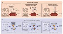
SignificanceLogic computing, a digital computational process grounded in Boolean logic, involves the processing of discrete signals through logic gates. It plays a pivotal role across numerous disciplines, including computer science, communications and electronics engineering, artificial intelligence, and emerging quantum computing, providing fundamental support for technological innovation and progress in modern information society. Chips serve as the hardware foundation for logic computing, executing fundamental computational tasks through logic circuits. These circuits, composed of tens of billions of transistors, enable chips to perform large-scale computations. The architectural design of a chip dictates its computational speed and efficiency, with distinct architectures tailored to specific computational tasks. Moreover, advancements in chip manufacturing technologies have fostered innovations in computational paradigms. Enhanced chip processes have led to devices with lower power consumption and greater performance, fueling the rapid expansion of big data, the Internet of Things, cloud services, and the rise of artificial intelligence. However, power consumption constraints have caused chip clock frequencies to plateau at a few gigahertz, and quantum uncertainty has rendered electronic transistors unreliable at nanoscale dimensions. Consequently, continued chip development is increasingly challenged in adhering to Moore’s Law. Additionally, the growing demand for computational power across emerging fields has exposed significant bottlenecks in traditional electronic computing, which reveals a substantial gap between current capabilities and actual requirements. Optical computing, with its advantages of high parallelism, low power consumption, low latency, and independence from advanced fabrication processes, offers a promising path to overcome Moore’s Law limitations. It holds the potential for the creation of high-performance, low-power chips. Extensive experience with digital circuits in very large-scale integration (VLSI) has demonstrated the critical role of logic computing due to its superior noise tolerance and high stability. By harnessing the low-power driving capabilities of optoelectronic devices, reconfigurable logic gates can execute a range of logic functions with ultra-low power consumption. The vast bandwidth of optical devices enables programmable logic arrays (PLAs) to dramatically enhance computational power. Additionally, the inherent speed of light propagation significantly reduces computational delays in arithmetic logic units (ALUs). Optical logic computing is emerging as a critical paradigm for the next generation of general-purpose photonic computing. While optical logic computing offers substantial performance benefits over traditional electronic chips, its large-scale implementation and application remain fraught with challenges. In recent years, discussions on its research progress and future development have been limited. Therefore, summarizing the existing research is essential to provide a sound foundation for the future trajectory of this field.ProgressWe provide an overview of the progress in optical logic computing and compare key metrics across different technological approaches. First, we define logic computing, discuss the conflict between computational power demands and chip development, and review recent advancements and landmark achievements in the field of optical logic computing. Then, we introduce the two primary paradigms of optical logic computing (Fig. 1): one based on linear and nonlinear optical effects for all-optical logic computing (Fig. 2), and the other based on thermo-optic, electro-optic, and phase-change effects for electro-optic logic computing (Fig. 5). These paradigms hold great promise for constructing high-speed, high-performance, and energy-efficient systems in the post-Moore era, where traditional electronic logic computing faces bottlenecks in computational power and energy consumption. They represent critical paradigms for the next generation of general-purpose photonic computing. The development of these paradigms has evolved from simple logic gates to programmable logic arrays, and further to general-purpose computing systems, such as state machines and cellular automata. Notably, progress has been made in overcoming bit-width limitations, with a shift toward three-dimensional integration. In addition, the emergence of more advanced logic paradigms in recent years, combined with the improvement of automated design methods, has propelled modularization. Hybrid digital-analog neural networks and two-dimensional cellular automata highlight the potential of optical logic computing to address large-scale computational tasks. We also explore the advantages, disadvantages, and potential breakthroughs of various technological routes (Tables 1 and 2), summarizing the significant challenges currently faced by both all-optical and electro-optical logic computing, including issues related to bit-width expansion, performance enhancement, energy consumption reduction, and programmability. Central challenges include excessive link loss, difficulties in cascading devices, and obstacles in restoring logic signals (Figs. 7 and 8).Conclusions and ProspectsThe performance enhancement of contemporary general-purpose computing systems relying on electronic architectures has hit a bottleneck. Optical logic computing presents an opportunity to achieve breakthroughs in computational power, energy efficiency, and parallelism. The first step towards realizing this vision is to overcome the bandwidth, switching power, and device losses associated with electro-optic logic modulators while developing optical parallel logic and electro-optic multi-level loading to address bit-width limitations. This helps bridge the gap from fully electronic to fully optical general-purpose computing using electro-optic logic. The second step involves optimizing the loss and energy consumption of nonlinear optical devices, developing parallelizable all-optical nonlinear modules, and configuring programmable, general-purpose all-optical logic arrays. As diverse optical logic computing devices and architectures are demonstrated, optical logic computing becomes a fundamental building block for achieving arbitrary functionality in digital computing. This will bring revolutionary performance advancements in applications such as data centers, ultra-parameterized large models, and supercomputers.
Jul. 25, 2025Vol. 45 Issue 14 1420001 (2025)
Qipeng Yang, Ye Tian, Shuhan Yue, Xueling Wei, Zenan Wu, Bowen Bai, Haowen Shu, Weiwei Hu, and Xingjun Wang
SignificanceThe rapid advancement of artificial intelligence, particularly deep learning, has created increasingly demanding requirements for hardware performance. Traditional electronic computing architectures encounter substantial limitations—including the deceleration of Moore’s Law and persistent challenges from the “memory wall” and “power wall”—restricting their capacity to maintain performance improvements for large-scale, highly concurrent AI tasks. This widening gap between computational requirements and hardware capabilities necessitates the exploration of alternative computing paradigms to overcome these fundamental constraints. Optical computing, utilizing the inherent properties of photons, emerges as a highly promising solution. Among various optical computing approaches, photonic neural networks (PNNs) have attracted considerable attention. PNNs employ photons directly to perform essential mathematical operations fundamental to neural networks, such as vector-matrix multiplication, convolution, and nonlinear activation functions. This natural capability to execute computation in the optical domain provides significant advantages over conventional electronic methods, including ultra-high processing speed, extensive bandwidth for data throughput, inherent parallelism, and substantially reduced energy consumption through minimized data transfer latency. Consequently, PNNs have emerged as a critical research frontier bridging photonics, information science, and artificial intelligence, offering an innovative solution for next-generation high-performance AI hardware. This review thoroughly examines PNNs’ core concepts, technological developments, and future directions.ProgressThis review systematically summarizes recent key technologies and progress in PNN physical implementations, organized by primary architectural types that have driven significant advancements in the field.PNNs based on diffractive optical elements, often referred to as diffractive optical neural networks (DONNs), harness the wave propagation of light through structured diffractive layers to perform all-optical deep learning inference. This architecture has demonstrated remarkable performance in tasks like complex image classification and reconstruction. Recent breakthroughs include the development of reconfigurable and programmable DONNs for multi-task learning, the integration of multi-dimensional multiplexing to significantly boost computational throughput, enhanced robustness against fabrication errors and environmental noise, and successful on-chip integration, paving the way for compact and efficient devices.PNNs based on Mach-Zehnder interferometer (MZI) arrays utilize reconfigurable MZI units to implement arbitrary linear optical transformations, establishing highly adaptable computational layers. Early theoretical designs have evolved into large-scale integrated MZI meshes that achieve high-accuracy classification and regression tasks, including complex-valued computations. Key advances include innovative architectural designs for enhanced scalability and energy efficiency, robust configurations addressing hardware imperfections and crosstalk, and sophisticated on-chip training methods for precise weight loading and adaptive operation in real-time.PNNs leveraging microring resonator (MRR) arrays utilize the distinctive wavelength-selective properties of microring resonators, particularly in wavelength division multiplexing (WDM) systems, to enable high-throughput parallel processing. The “broadcast-and-weight” architecture establishes a fundamental paradigm for MRR-based PNNs, enabling dynamic weight modulation and optical summation. Notable advances include sophisticated weight bank control for high-precision tuning, innovative architectural designs for integrated tensor computations and optical convolutions at impressive computation densities, and the integration of diverse functionalities for specialized applications, demonstrating their potential for ultra-compact and high-performance computing.PNNs based on cascaded modulator architectures achieve complex optical transformations through the sequential modulation of optical signals, offering structural simplicity and high integration potential. These architectures have demonstrated ultra-low energy consumption per operation and high accuracy in classification tasks like MNIST digit recognition. Recent advancements focus on direct cascaded modulator systems, robust hybrid optoelectronic integration for versatile control and non-linearity, coherent processing architectures for high-precision complex-valued computations, and programmable signal processors for reconfigurable and high-speed inference, pushing the boundaries of compact integrated photonic circuits.Finally, the implementation of optical nonlinear activation functions is crucial for enabling deep learning capabilities in PNNs, allowing networks to learn and process complex, non-linear relationships. Two primary categories are distinguished: optoelectronic hybrid methods, which convert optical signals to electrical for nonlinear processing before re-converting, and all-optical methods, which directly exploit intrinsic material nonlinearities or specific device effects (Figs. 20?22). Progress in this area is vital for constructing truly multi-layered PNNs that can break linearity and achieve high accuracy across diverse and challenging AI tasks.Conclusions and ProspectsWhile PNN research has achieved significant progress, substantial challenges remain. These include achieving high level integration and scalability for complex tasks, improving power efficiency of active photonic components, enhancing robustness against manufacturing errors and environmental noise, realizing efficient all-optical nonlinear activation for deep networks, and developing practical on-chip optical memory. Future development requires multidisciplinary innovation, emphasizing novel materials and computing elements, co-design of hardware and algorithms, advanced photonic integration platforms, and expanding PNN applications into scientific computing, optimization, simulation, and advanced sensing. Addressing these challenges will enable PNNs to evolve from prototypes to practical solutions, establishing their position in post-Moore computing.
Jul. 22, 2025Vol. 45 Issue 14 1420002 (2025)
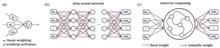
Chaoran Huang, Shaojie Liu, Benshan Wang, Dongliang Wang, Yikun Nie, and Tengji Xu
SignificanceThe exponential growth of artificial intelligence (AI), particularly large-scale neural network models, has led to unprecedented demands on computational power. Traditional electronic computing platforms face significant challenges in meeting these demands due to the breakdown of Moore’s law, the inefficiency of the von Neumann architecture, and the high energy consumption associated with data movement between memory and processing units. These limitations become critical when scaling deep learning models, which increasingly rely on massive parallel matrix computations and nonlinear operations.Photonic computing, leveraging the intrinsic advantages of light—including high bandwidth, parallelism, and ultra-low latency—has emerged as a compelling alternative. Unlike electronics, photons can propagate without resistive loss and interference, offering superior energy efficiency and speed. Among various photonic computing architectures, microring resonator (MRR)-based systems are particularly promising due to their small footprint, low tuning energy, and compatibility with dense wavelength-division multiplexing (WDM). MRRs not only support scalable and reconfigurable linear operations, such as matrix-vector multiplication, but also exhibit rich nonlinear dynamics arising from Kerr effects, two-photon absorption (TPA), free-carrier effects, and thermo-optic responses. These properties make them well-suited for implementing both the linear weighting and nonlinear activation functions essential in neural network computation. Furthermore, MRRs offer an advantageous platform for building on-chip spiking neurons and all-optical signal processors, which could play a vital role in neuromorphic and event-driven computing paradigms.As silicon photonics technology matures and large-scale integration becomes feasible, MRR-based systems are expected to provide compact, high-speed, and energy-efficient photonic processors that are well-aligned with the growing requirements of AI workloads in the post-Moore era.ProgressRecent research has demonstrated the feasibility of MRR-based photonic computing systems for both linear and nonlinear tasks. Linear matrix-vector multiplication can be implemented by broadcast-and-weight architecture or crossbar arrays (Figs. 3?4), where input vectors are encoded onto different wavelengths and processed in parallel. In addition, several new computing architectures have been proposed to enhance functionality, including support for optical convolution, bidirectional signal propagation for in-situ training, and high-dimensional tensor computation through mode and frequency multiplexing (Fig. 5).Nonlinear operations are achieved either all-optically, through the intrinsic nonlinear response of MRRs (Figs. 6?8), or via hybrid optical-electrical-optical (OEO) pathways (Fig. 9). Reconfigurable optical activation functions have been experimentally demonstrated using a range of mechanisms, including MRR-assisted Mach-Zehnder interferometers, thermally tunable phase-change materials, and dynamic modulation of free-carrier density (Fig. 7). These schemes allow for the emulation of activation functions like ReLU, Sigmoid, Softplus, and Radial Basis functions. Additionally, MRR-based photonic neurons have been used to simulate biological spiking neuron behavior, including threshold firing, temporal integration, and refractory periods. These devices achieve nanosecond- to picosecond-scale pulse responses depending on their material system and design (Fig. 8). Multiple OEO photonic neuron designs based on MRRs have been demonstrated, enabling reconfigurable and cascadable nonlinear transfer functions. They have been integrated into end-to-end deep photonic neural networks and have shown strong potential in real-time signal processing (Fig. 9).Integrated system-level demonstrations include both deep optical neural networks (DONNs) and reservoir computing frameworks. DONNs based on MRRs have exhibited competitive performance in image classification, optical fiber communication signal equalization, and speech recognition tasks, achieving high throughput and low latency in a compact footprint [Figs. 10(a)?(c)]. Meanwhile, MRR-based optical reservoir computing systems, enabled through spatial and temporal multiplexing strategies, have been used to implement time-series tasks such as binary logic, waveform prediction, and speech classification with minimal training overhead [Figs. 10(d)?(f)].To support high-precision computation, researchers have proposed various calibration and control techniques. These include feedback-based thermal tuning, dual-wavelength monitoring, dithering modulation, and so on, achieving weight tuning precision of over 9 bit (Fig. 11). Additionally, to further enhance network robustness against fabrication variations and environmental drift, novel training techniques such as noise-injection training, optical pruning, and sharpness-aware training have been introduced (Fig. 12).MRR-based computing has also been demonstrated in a variety of practical applications across different domains (Fig. 13), such as solving differential equations, optical image convolution and classification, and signal equalization and compensation. These demonstrations highlight the versatility and scalability of MRR systems, and show their potential for integration into real-world intelligent processing systems.Conclusions and ProspectsMRR-based photonic computing offers a promising path forward for energy-efficient and scalable AI hardware. With the ability to perform both linear and nonlinear computations in compact, low-power photonic circuits, MRRs are well suited for next-generation intelligent systems. Challenges remain, particularly in improving computing precision, robustness against ambient fluctuation and noise, and scaling to large-scale end-to-end networks. However, ongoing research into calibration-free control methods, innovative computing architecture, and advanced integration techniques are steadily addressing these issues. Looking ahead, further innovations in photonic device design, integrated control circuits, and system-level architectures will be crucial for advancing MRR-based computing from lab-scale demonstrations to practical, large-scale deployment.
Jul. 21, 2025Vol. 45 Issue 14 1420003 (2025)
Hao Wang, Ziyu Zhan, Xing Fu, and Qiang Liu
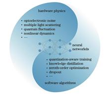
SignificanceDeep neural networks (DNNs) have revolutionized traditional approaches across numerous scientific and technological domains, demonstrating exceptional performance in computer vision, natural language processing, speech recognition, and recommendation systems. While these networks rely on sophisticated models with extensive parameters, the underlying computing hardware plays a crucial yet often overlooked role. Each advancement in DNNs correlates directly with hardware capability improvements. As contemporary computing chips approach Moore’s law limitations, the computational power requirements continue to escalate. Consequently, both academic and industrial sectors are investigating alternative physical computing platforms, including in-memory computing. Optical computing emerges as a promising solution, harnessing light’s inherent multidimensional properties and light-matter interactions to develop optical or optoelectronic information processing systems. With distinct advantages including low latency, high parallelism, low power consumption, and large bandwidth, optical computing distinguishes itself in the development of “non-Von Neumann” integrated storage-computation platforms, achieving notable progress in recent years.ProgressSignificant advancements have emerged in accelerating neural network computations through optical systems, specifically optical neural networks (ONNs). Researchers have developed programmable photonic chips implementing linear matrix-vector multiplication via arrays of Mach-Zehnder interferometers (MZIs), micro-ring resonators (MRRs), and phase change materials (PCMs). Furthermore, they have investigated novel optical computing platforms including multi-layer diffractive neural networks, scattering media, and multimode fibers. These optical computing systems utilize spatial, temporal, and frequency modes in optics, or parallel combinations thereof, consistently advancing computational performance in optical neural networks. Present research in optical computing emphasizes hardware development, with hardware innovations frequently garnering substantial attention. The integration of software algorithms with optical computing hardware’s physical characteristics has received relatively less focus. However, algorithmic progress has substantially enhanced optical neural networks, demonstrating that effective hardware-software synergy yields significant research achievements. This paper provides a systematic review of the relationship between optical computing hardware’s physical characteristics and software algorithms (Fig. 1). The analysis examines how algorithmic advances enhance optical computing hardware performance (algorithm-enhanced ONN), particularly focusing on optimization techniques improving hardware processing capacity and efficiency (Figs. 2?6). Additionally, it explores how optical computing hardware’s unique physical properties can integrate with and enhance algorithms, termed hardware-inspired optical neural networks (hardware-inspired ONN) (Figs. 7?9). The paper concludes with perspectives on optical neural network development trends.Conclusions and ProspectsDespite significant progress and achievements in ONNs, the field remains relatively nascent compared to established electronic neural networks. This review examines the integration of hardware physics and algorithms in ONN development. The analysis reveals that collaborative design between hardware physics and software algorithms is fundamental for maximizing optical computing potential in machine learning applications. The 2024 Nobel Prize in Physics recognition of the Hopfield model and Boltzmann machines emphasizes the significance of physics-machine learning bidirectional interactions. In optical computing, algorithmic advances have enhanced simulated optical computing system stability, while optical physical phenomena have inspired novel model architectures extending beyond traditional neural network frameworks. The optical nonlinear Schr?dinger equation, for instance, has been adapted into a trainable model for physics-informed neural networks, generating several innovative architectural approaches. Through examining hardware-algorithm synergies, this review aims to stimulate mutual engagement between optics and algorithm development researchers, advancing the interdisciplinary field of optical neural networks. Additionally, it seeks to establish a sustainable development trajectory for optical computing through dynamic optical physics and machine learning interactions.
Jul. 22, 2025Vol. 45 Issue 14 1420004 (2025)
Xingxing Guo, Zhiwei Dai, Shuiying Xiang, Hanxu Zhou, Yahui Zhang, Yanan Han, Changjian Xie, Tao Wang, and Yue Hao
SignificanceIn recent years, as an important driving force for the new round of technological revolution and industrial transformation, artificial intelligence technology has shone brightly in the fields of big data, cloud computing, the Internet of Things, data centers, and radio management. At the same time, the rapid development of artificial intelligence and information technology has also led to an explosive growth in the scale of information that needs to be processed globally. However, due to the bottleneck of high-end semiconductor manufacturing processes in China, traditional “von Neumann” architecture-based electronic processors struggle to support the requirements for computing power and energy consumption. Therefore, the search for a new type of computing with fast information processing speed and low power consumption has become a major challenge for artificial intelligence technology. Neuromorphic computing is a type of computing method that simulates the information-processing process of the human brain. Since its emergence, it has attracted great attention. Among these, reservoir computing (RC), as a simple and efficient neuromorphic computing framework similar to the cortical circuits of the human brain, has received much attention. The core idea is to use the dynamical system as a reservoir layer (nonlinear generalization of the standard basis) to adaptively learn spatiotemporal features and hidden patterns in complex time series. Traditional recurrent neural networks face problems such as low computing efficiency, complex training algorithms, and easy entrapment in local optima, while reservoir computing has the advantages of fast learning speed and low training cost. In addition, the rapid development of photonics technology and optical devices has also brought new opportunities to optical information processing. Photonic reservoir systems, with their remarkable advantages of high speed, low latency, wide bandwidth, and multi-dimensionality, have quickly become a research hotspot.ProgressThe theoretical and experimental research on photonic RC has rapidly progressed along two main directions. The first direction involves the construction of spatially distributed array photonic RC systems with multiple physical nodes. In this approach, various photonic devices are carefully selected and arranged to form specific spatial array structures, creating a photonic reservoir. By leveraging the propagation and interaction of photons among these nodes, the system can perform complex processing of input optical signals to accomplish corresponding computational tasks. This direction can be further divided into two sub-approaches: one uses multiple optical devices as nonlinear nodes—such as semiconductor optical amplifiers (SOAs) and microring resonators—and constructs optical networks through waveguide coupling (Fig. 2). The other focuses on free-space optical modulation, utilizing components like spatial light modulators (SLMs) and diffractive optical elements (DOEs). These systems achieve spatial distribution through methods such as secondary imaging and phase modulation, forming spatially distributed array photonic RC systems (Fig. 3).The second direction centers on building nonlinear photonic reservoirs using different optical devices and delayed feedback loops. Based on the principle of time-division multiplexing, equally spaced sampling points along the feedback loop are used to replace real physical nodes in space, resulting in hardware-friendly time-delay photonic RC systems. This paper focuses on time-delay RC systems based on semiconductor lasers (Fig. 7 and Fig. 10). Finally, this paper also discusses the challenges faced in this field and the emerging research directions, including the deployment of photonic RC in practical applications, the lack of universal reservoir operators, the implementation of all-optical reservoirs, and the gap between existing results and solving real-world problems.Conclusions and ProspectsPhotonic RC hardware demonstrates vast application potential in cutting-edge fields such as 6G communications, next-generation optical networks, the internet of things (IoT), green data centers, intelligent robotics, and digital twins, and is expected to become a core driving force for technological innovation and industrial upgrading. However, despite its potential for large-scale deployment, photonic RC still faces numerous challenges in practical implementation. On the theoretical front, current universal approximation theories mainly focus on existence proofs, lacking the design of general-purpose operators based on reservoir architectures and the realization of reconfigurable universal computation grounded in such reservoirs. In data-driven control applications, the output layer of existing reservoir computing frameworks still relies heavily on digital software-based implementations. How to design a fully hardware-based output layer, ultimately achieving all-optical reservoir computing, remains a major challenge for researchers. From an algorithmic perspective, although reservoir computing holds significant promise, a gap still exists between current research outcomes and the ability to solve complex, real-world problems. Coordinated breakthroughs in structural design, theoretical analysis, algorithm optimization, and hardware integration are urgently needed to bring reservoir computing into practical, real-world applications.
Jul. 25, 2025Vol. 45 Issue 14 1420005 (2025)
Ruizhe Liu, Zijia Wang, and Hongtao Lin
SignificanceThe rapid advancement of artificial intelligence (AI) technologies is driving transformative changes across multiple industries including scientific research, automated manufacturing, healthcare, service sectors, and autonomous transportation. This AI revolution has created unprecedented demands for computational power and energy efficiency. Traditional electronic computing architectures struggle to meet the fundamental limitations of Thevon Neumann architecture, particularly the “memory-wall” problem arising from the physical seperation of processing and memory units, which leads to excessive energy consumption during data transfer operations. Furthermore, the approaching physical limits of semiconductor miniaturization under Moore’s Law severely constrain further improvements in processor clock speeds.Optical computing has emerged as a promising alternative paradigm to address these critical challenges. By utilizing photons instead of electrons as information carriers, photonic computing systems offer several inherent advantages: (1) massive parallelism enabled by wavelength division multiplexing and optical interference phenomena, (2) near-zero heat dissipation during information transmission, (3) ultra-high bandwidth capabilities exceeding 100 GHz, and (4) light-speed processing latency. These characteristics make photonic neural networks particularly well-suited for accelerating matrix-vector multiplications, which constitute over 90% of computations in deep learning models.However, within integrated photonic neural networks, implementing efficient nonlinear activation functions remains a significant technical challenge. While linear operations can be effectively performed using Mach-Zehnder interferometer arrays or microring resonator weight banks, introducing essential nonlinear transformations is problematic. Current hybrid photonic-electronic systems typically offload nonlinear activation to electronic processors, creating substantial bandwidth bottlenecks and energy overhead at the optoelectronic interfaces. This architectural limitation undermines many potential advantages of all-optical computing systems.Therefore, the development of high-performance and programmable optical nonlinear activation devices is crucial for realizing end-to-end optical neural networks. Successful implementation would enable: (1) orders-of-magnitude improvements in processing speed by eliminating electro-optic conversion delays, (2) dramatic reductions in power consumption through all-optical signal processing, and (3) novel computing architectures leveraging quantum optical effects. These advancements could revolutionize AI hardware for applications ranging from real-time video analysis to large language model inference, potentially reducing energy consumption by several orders of magnitude compared to conventional electronic processors.ProgressRecent years have witnessed significant advancements in on-chip optical activation functions, progressing primarily along two technical pathways: electro-optic and all-optical implementations.Electro-optic approaches, currently the most mature technological solution, leverage established silicon photonics manufacturing. These systems typically employ a three-stage architecture: optical-to-electrical conversion via photodetectors, electronic nonlinear processing, and electrical-to-optical modulation. The ITO-based electro-absorption modulator platform has demonstrated notable promise, achieving 98% accuracy on MNIST classification tasks with 5 mW threshold power. Recent innovations using graphene-ITO heterostructures have further reduced operating voltages to sub-1 V levels while maintaining favorable nonlinear response characteristics. However, these devices face inherent tradeoffs between speed (typically limited to ~100 ps by carrier dynamics) and energy efficiency (usually >1 pJ/operation). Novel integration schemes are addressing these limitations: the ECU-ORS-MZI configuration incorporates non-volatile MoS2-based optoelectronic memory switches, enabling reconfigurable activation functions (Sigmoid, Softplus, Clamped ReLU) with only 2 V drive voltage. More radically, graphene-silicon heterojunction devices integrate detection and modulation functionalities within a single microring resonator, achieving 8 μW threshold power through innovative photocurrent contour mapping techniques. While these co-designed systems show promise for reducing device footprints and power consumption, challenges persist in scaling large arrays while maintaining uniformity.All-optical nonlinear activation represents the ultimate solution for photonic neural networks, with breakthroughs across multiple material platforms: silicon photonic devices exploit combinations of Kerr nonlinearity, two-photon absorption, and free-carrier effects. MRR-MZI configuration achieves 25 mW/π thermal tuning efficiency with 2.5 ns response, while inverse-designed nanostructures reduce optical power thresholds to 2.9 mW. Emerging silicon nitride platforms enable 10 Gbit/s operation using pure Kerr nonlinearities with negligible absorption loss. Germanium-based devices leverage strong absorption characteristics and carrier plasma effects. Ge-Si photodiode architecture operate at 20 GHz with 1.1 mW threshold power, while microring versions achieve 0.74 mW thresholds via innovative thermal feedback loops. These devices show excellent compatibility with standard CMOS processes. Lithium niobate platforms exploit large second-order nonlinear coefficients. The SHG-DOPA configuration demonstrates record 16 fJ thresholds and 75 fs response time, with periodically poled waveguides suggesting further energy reductions. Phase change materials enable non-volatile state switching: GST-based microrings achieve 500 pJ switching energy with <200 ns crystallization time, while VO? devices show 0.5 mW threshold and broadband operation (visible to near-infrared wavelengths), supporting in-memory computing architectures. Two-dimensional materials offer exceptional versatility: graphene-plasmonic hybrids reach 35 fJ threshold and 260 fs response time using universal absorption. MXene devices operate at 50 μW across 1310?1550 nm bands, while MoTe2-glass waveguide systems achieve 0.94 μW threshold with 2.08 THz bandwidth, highlighting multi-wavelength parallel processing potential.Conclusions and ProspectsThe field of on-chip optical activation functions has achieved remarkable progress through both electro-optic and all-optical approaches, each offering distinct advantages. Future research directions should prioritize three critical directions: (1) wafer-scale heterogeneous integration of novel materials (2D materials, PCMs) with standard photonic platforms, (2) development of standardized programming interfaces for optical nonlinearities, and (3) system-level solutions for maintaining signal integrity in multi-layer networks. Hybrid approaches combining complementary platforms may provide near-term pathways while fundamental material challenges are resolved. With continued advances in materials science, nanofabrication techniques, and photonic design methodologies, optical neural networks incorporating efficient nonlinear activation functions could soon achieve the transition from laboratory demonstrations to commercial deployment, potentially revolutionizing energy-efficient AI computing across diverse application domains.
Jul. 25, 2025Vol. 45 Issue 14 1420006 (2025)
Can Huang, Wentao Hao, Jingsong Fu, Haoliang Liu, Limin Jin, Yidong Wang, Ruiheng Jin, Junyan Chen, Zhaohui Xie, and Yue Cui
SignificanceWith the rapid development of emerging technologies such as big data, the Internet of Things, and artificial intelligence, the performance requirements for computing systems are ever-increasing. Conventional computing hardware, centered on microelectronic technologies, faces fundamental limitations in speed, power consumption, and parallelism, especially when handling complex computational tasks. This has spurred the exploration of novel computing architectures based on new physical mechanisms. Analog optical computing, which leverages the intrinsic physical properties of systems to process information, has emerged as a promising paradigm, offering new solutions by leveraging the advantages of photons, such as high-speed transmission, high bandwidth, and low power consumption. While significant progress has been made in optical neural networks based on coherent waveguide arrays and spatial diffraction, these schemes often utilize only the linear optical response of devices. The lack of tunable nonlinear mechanisms limits their computational power, as real-world information processing tasks are inherently nonlinear. Semiconductor lasers are complex nonlinear dynamical systems as cornerstone of photonics, making them ideal physical platforms for analog optical computing. Their rich dynamics, including periodic oscillations and chaos induced by external perturbations such as optical injection, delayed feedback, and mutual coupling, provide a powerful resource for computation. Moreover, a network of coupled lasers can spontaneously evolve, through physical processes such as mode competition, into a stable minimum-loss state that maps directly to the solution of a specific mathematical optimization problem. Crucially, unlike many optical schemes that only implement linear matrix operations, systems based on semiconductor laser dynamics can realize both linear weighted summation (through injection and coupling) and key nonlinear activation functions (through intrinsic mechanisms like thresholding, gain saturation, and mode competition) within a single device. This allows them to function as complete neural units. Coupled with recent advancements in integrated micro- and nano-photonics, which enable high-density and on-chip integration, the study of semiconductor laser dynamics offers a compelling pathway toward scalable, high-performance, and brain-inspired analog optical computing systems.ProgressThis review systematically elaborates on the applications of semiconductor laser dynamics in analog optical computing, focusing on several representative neuromorphic computing paradigms. First, reservoir computing (RC) is discussed, a recurrent neural network framework where only the output layer is trained. We focus on the time-delay architecture, where a single nonlinear node with delayed feedback can emulate a large network of virtual nodes. A semiconductor laser with optical feedback serves as an ideal nonlinear node, performing high-dimensional mapping of input signals [Fig. 3(c)]. The computational performance of such a system critically depends on the delicate balance between consistency and memory capacity, with the optimal operating point often found at the edge of injection locking, where the system retains a rich nonlinear transient response while ensuring reproducibility [Fig. 3(d)]. Recent progress includes the use of vertical cavity surface emitting laser (VCSEL) polarization dynamics to enhance memory capacity, as well as the development of parallel and deep RC architectures on photonic integrated circuits to improve processing capacity and task-specific performance. Second, photonic spiking neural networks (SNNs) are explored, which mimic the behavior of biological neurons. The dynamics of a two-section semiconductor laser with a saturable absorber (SA) can physically emulate the leaky integrate-and-fire (LIF) neuron model [Fig. 4(b)]. Here, the accumulation of carriers in the gain section corresponds to membrane potential integration, while the bleaching of the SA triggers a sharp optical pulse, analogous to a neuron firing. Recent works have extended this concept to replicate a richer set of biologically-plausible neuronal behaviors, including phasic spiking, tonic spiking, and controllable inhibition, by leveraging the complex dynamics of optically-injected VCSELs. Furthermore, other physical mechanisms, such as those in excitable lasers and distributed feedback (DFB) lasers, have been used to demonstrate functionalities like graded-potential signaling and pulse facilitation, laying a solid foundation for more brain-like computing systems. Third, optical Ising machines are reviewed, which solve complex combinatorial optimization problems by finding the ground state of an Ising Hamiltonian [Fig. 5(a)]. The core concept in semiconductor laser-based systems is the use of an injection-locked laser network, where the state of each laser (e.g., polarization) represents an Ising spin. The system spontaneously evolves through mode competition to a global minimum-loss state, which corresponds to the solution of the optimization problem [Figs. 5(b) and (c)]. We highlight the latest advancements toward scalable, all-optical systems using VCSEL arrays coupled with programmable spatial light modulators (SLMs). This approach aims to eliminate electronic bottlenecks by enabling fully programmable coupling matrices, with recent work demonstrating its feasibility through simulations and proof-of-concept experiments, promising an on-chip path toward large-scale optical spin systems. Finally, optical reinforcement learning (RL) is introduced, which tackles decision-making in uncertain environments. We detail the development path from early concepts using laser chaos as a high-speed physical random number generator to more sophisticated schemes that directly control the laser’s internal dynamics. The state-of-the-art is exemplified by the use of chaotic itinerancy in a multimode semiconductor laser [Fig. 6(b)]. In this scheme, different longitudinal modes of the laser correspond to different actions, the natural chaotic hopping between modes provides an intrinsic “exploration” mechanism, and selective optical injection is used to reinforce successful actions, corresponding to the “exploitation” phase [Fig. 6(c)]. This elegant mapping of the exploration-exploitation dilemma onto a physical process has demonstrated superior scalability compared to traditional algorithms.Conclusions and ProspectsThe research surveyed in this paper demonstrates that the nonlinear dynamics of semiconductor lasers provide a versatile and powerful physical basis for a variety of brain-inspired analog computing paradigms. However, significant challenges remain on the path to practical application. Current systems are often limited in scale and rely on discrete, fiber-coupled components, which are constrained by coupling efficiency and the inherent speed limitations of semiconductor carrier lifetimes. Scalability is a major bottleneck, as the number of nodes increases, the parameter space of the coupling network expands dramatically, making global control complex and fragile. These challenges highlight a fundamental conflict between systems based on discrete components and the technological trend toward high-density photonic integration. Looking forward, the rapid advancements in micro- and nano-lasers offer a promising path to overcoming these limitations. Micro- and nano-scale devices provide significant advantages in terms of reduced size, enhanced coupling efficiency, and faster dynamic response due to effects like Purcell enhancement. The synergy of theoretical modeling and algorithm design must be deepened to guide the structural design of these complex networks. Furthermore, exploiting multidimensional multiplexing of the optical field and leveraging novel physical mechanisms unlocked by non-Hermitian and topological photonics will be crucial. The precise control afforded by these new physical frameworks may lead to novel functionalities and more robust computational systems. In conclusion, the convergence of semiconductor laser dynamics, micro- and nano-photonics, and artificial intelligence algorithms represents a vibrant and promising field of research, poised to contribute significantly to the development of next-generation intelligent analog optical computing systems.
Jul. 17, 2025Vol. 45 Issue 14 1420007 (2025)
Tonglu Wang, Yuyan Wang, Jiyuan Zheng, Chenchen Deng, Jingtao Fan, and Qionghai Dai
SignificanceThe technical framework of optoelectronic hybrid intelligent computing chips focused on artificial intelligence tasks has demonstrated substantial advancement in recent years. This architecture integrates electronic computing flexibility with optical computing advantages of high bandwidth and low power consumption, establishing a promising direction for overcoming traditional electronic computing limitations. Additionally, intelligent all-optical computing technology has emerged as a potential solution for future computing requirements. Through all-optical processing of information transmission and processing, this technology aims to fundamentally address energy consumption and latency issues associated with optical-electrical signal conversion. However, current optoelectronic hybrid chip development remains constrained by optoelectronic signal conversion efficiency, with optical detection and signal conversion technology representing critical bottlenecks.ProgressOptical detection chips serve as essential components in intelligent optical computing systems, demonstrating crucial significance. These chips exhibit high sensitivity and broad wavelength response ranges, enabling precise optical signal reception and conversion while providing reliable data input for intelligent optical computing. Their high integration and intelligent characteristics fulfill optical computing architectural requirements, integrating effectively with light sources, modulators, and other optoelectronic devices to establish compact and efficient optical computing systems capable of large-scale parallel processing. Furthermore, advances in miniaturized packaging technology enable optical detection chips to operate stably within confined spaces, ensuring compact layout and reliable long-term operation of intelligent optical computing devices while enhancing overall system efficiency. Although new photodetectors demonstrate improved performance through novel materials and structures, comprehensive considerations regarding efficiency and power consumption remain crucial in intelligent optical computing applications. This article examines optical detection and signal conversion in optical detection chips, analyzing photodetector basic principles and structures (Fig. 1) and specific requirements for intelligent optical computing scenarios. It explores two optical coupling forms in optical detection chips: surface incident photodetectors (Figs. 2‒3) and waveguide coupled photodetectors (Fig. 4), presenting relevant applications and comparing their advantages in different intelligent optical chip scenarios. Additionally, it examines integrated optical detection chips and contrasts two system architectures: photodetection and computing separation (Fig. 5) and photodetection and computing integration (Fig. 6). Finally, it synthesizes relevant parameters of on-chip photodetectors in current intelligent optical computing applications and outlines development paths for performance optimization, enhanced optoelectronic device integration, and industrial advancement.Conclusions and ProspectsThe requirements of intelligent all-optical computing have catalyzed technological advancement in optical detection chips. Current development focuses on achieving multi-material functional integration through heterogeneous integration, increasing density via 3D stacking and wafer-level packaging, and optimizing performance through combined photoelectric and thermal simulation. These advancements will propel all-optical computing chips toward enhanced computing power density and energy efficiency, potentially surpassing electronic computing limitations, enabling high-performance computing architectures, advancing artificial intelligence and big data processing, and facilitating photonic chip development and industrialization.
Jul. 14, 2025Vol. 45 Issue 14 1420008 (2025)
Shuying Li, Yunping Bai, Haoran Zhang, Shifan Chen, Jiajia Wang, Xuecheng Zeng, Xingyuan Xu, and Kun Xu
SignificanceThe rapid advancement of artificial intelligence, cloud computing, and high-throughput data processing presents significant challenges to traditional electronic computing systems, which face limitations in power consumption, signal delay, and CMOS technology scaling constraints. Optoelectronic intelligent computing chips (OICCs) have emerged as an innovative computing paradigm that utilizes photons for information transmission, enabling parallel processing, ultra-high-speed operations, and energy efficiency. These chips are positioned to serve as fundamental components in next-generation computing platforms, particularly in demanding applications such as optical signal processing, artificial intelligence acceleration, and quantum information science.Among various architectures, MZI-based photonic computing structures are widely adopted due to their compact footprint, compatibility with silicon photonics platforms, and ability to perform unitary transformations via programmable phase shifts. However, the precise functionality of these chips is often compromised by fabrication-induced parameter variability, accumulated phase errors in complex interferometric paths, and thermal or environmental disturbances. Traditional static calibration or manual tuning is insufficient for maintaining computational precision in dynamic environments. Hence, the introduction of self-configuration algorithms is essential to endow OICCs with adaptive, robust, and scalable capabilities, making them viable for practical deployment in real-world applications.ProgressThis review offers a comprehensive survey of recent developments in self-configuration algorithms designed for MZI-based OICCs, covering their architectural foundations, algorithmic strategies, and typical application scenarios.We first analyze the programmable nature of 2×2 MZI units and the topological configurations used to build higher-dimensional matrix processors. Forward-only propagation meshes, including triangular and rectangular grids (Fig. 2), offer low-latency, linear transformation capabilities. Meanwhile, cyclic mesh topologies such as quadrilateral, hexagonal, and triangular structures (Fig. 3) provide higher functional density and support feedback paths, essential for realizing optical delay lines, resonant structures, and advanced signal processing functions.To manage the complexity of tuning such large-scale photonic networks, several algorithmic self-configuration paradigms have been introduced.Online training algorithms facilitate real-time parameter adjustment based on system feedback. A prominent approach is gradient-based optimization (Fig. 5), which determines the partial derivatives of an objective function with respect to tunable parameters like phase shifters. This can be implemented through forward propagation, finite difference methods, or in situ optical backpropagation. Recent studies incorporate adaptive learning strategies such as Adam optimizers and direct-derivative computation to accelerate convergence and enhance tolerance to system noise.In addition, bio-inspired global optimization techniques, such as Genetic Algorithms (GA) and Bacterial Foraging Optimization (BFO) (Figs. 6 and 7), are employed to explore complex solution landscapes. These methods, by simulating biological evolution or microbial behavior, have demonstrated strong adaptability in solving non-convex optimization problems across varying operating conditions.Reference-path-assisted techniques (Fig. 8) represent another significant class of online strategies. By introducing an on-chip optical reference path and exploiting Fourier or Kramers-Kronig relations, both amplitude and phase responses of the signal processing core can be recovered and optimized. These approaches circumvent the need for explicit phase measurement and offer robustness against thermal cross-talk and fabrication-induced loss imbalance, making them ideal for stable and accurate chip configuration.Offline training strategies predefine optimal control parameters based on empirical models or data under ideal conditions. One classic method is backpropagation combined with stochastic gradient descent (Fig. 9), where a neural network’s weights are trained off-chip and then mapped to the MZI phase matrix on-chip. Structural calibration and error compensation approaches (Fig. 10) address physical non-idealities by characterizing and correcting device-level deviations, enhancing functional reliability without additional hardware overhead. Noise-robust designs (Fig. 11) incorporate regularization and quantization strategies to maintain computational fidelity under environmental and circuit-level disturbances. Lastly, heuristic global optimization techniques such as hybrid genetic algorithms or simulated annealing (Fig. 12) enable efficient configuration of high-dimensional photonic arrays.Conclusions and ProspectsSelf-configuration algorithms are now recognized as the cornerstone technology enabling practical and large-scale deployment of optoelectronic intelligent computing chips. By tightly integrating optimization algorithms with chip-level hardware control, these systems achieve real-time sensing, autonomous decision-making, and adaptive reconfiguration. The result is a class of computing chips that not only perform complex linear and nonlinear operations but also self-optimize to maintain performance across diverse tasks and unpredictable operating environments.In application, self-configurable OICCs have demonstrated significant potential. In photonic signal processing, they enable all-optical logic gates, channel routing, and wavelength-selective filters with automatic tuning and recalibration. In artificial intelligence acceleration, they support matrix-vector multiplication and inference in optical neural networks with substantially improved energy efficiency and reduced latency compared to conventional GPU or TPU-based platforms. For example, the “Taichi” architecture, leveraging configurable MZI arrays, achieved near-human performance on large-scale classification tasks, demonstrating the feasibility of programmable photonic computing at scale. In quantum information, the high precision afforded by self-configuration allows robust realization of quantum logic gates, entangled photon state control, and reconfigurable quantum networks using photonic circuits.Despite significant advances, several critical challenges persist. These encompass improving phase-tuning resolution at the hardware level, implementing efficient feedback control mechanisms, and resolving scalability issues in multi-layer or multi-core photonic architectures. Future research directions may encompass the integrated design of algorithms and photonic device physics, incorporation of AI-based meta-learning for autonomous calibration, and utilization of edge-cloud collaborative frameworks for distributed self-configuration.In conclusion, self-configuration algorithms represent a fundamental enabler for transforming photonic computing from laboratory prototypes into practical systems. Through sustained interdisciplinary innovation, these methodologies will facilitate new possibilities for intelligent, scalable, and energy-efficient computing within the optical domain.
Jul. 22, 2025Vol. 45 Issue 14 1420009 (2025)
Yuchao Zhang, Qiming Zhang, and Min Gu
SignificanceArtificial intelligence (AI) has achieved remarkable success across various domains of modern society, including large language models (LLMs), autonomous driving, computer vision, and related fields. However, as Moore’s Law approaches its limits, electronic transistor technology faces fundamental physical constraints in speed and energy efficiency, making traditional electronic hardware improvements increasingly unsustainable. Optical neural networks (ONNs) emerge as a solution to address these electronic platform limitations. ONNs present significant advantages, including rapid computational speed, high parallelism, superior energy efficiency, and minimal crosstalk, positioning them as a promising candidate for next-generation high parallelism computing platforms. Recent advancements in artificial intelligence and micro/nano-fabrication technologies have facilitated significant breakthroughs in ONN architecture and integration methods. The architectural evolution of ONNs has produced diverse implementations, encompassing optical matrix multiplication, diffractive deep neural networks (D2NNs), photonic reservoir computing, convolutional ONNs, and photonic memristors. Additionally, through advances in nanophotonics and the utilization of on-chip photonic components, such as microcombs, micro-ring resonators, and Mach-Zehnder interferometers, ONNs have achieved increased compactness and integration, enabling collaboration with electronic components in hybrid optoelectronic neural networks.ONNs demonstrate in-memory computing capabilities, coupled with high neuron density, enhanced parallelism, minimal latency, and reduced power consumption, establishing a novel approach to physical AI computing. While optical architectures show exceptional energy efficiency potential (>74 POPS/W) in large-scale matrix computations compared to electronic neural networks, they continue to face challenges in reconfigurability, in-situ training, and on-chip integration levels. This paper examines the development history of ONNs from architectural and fabrication perspectives, analyzing the evolutionary trends of various ONN implementations and their potential commercialization in edge computing and real-time signal processing applications.ProgressThe brief history of ONNs is reviewed. First, we introduced the optical matrix multiplication (Fig. 1). The earliest optical matrix multiplication dates back to the 1960s. With the development of nanofabrication methods, on-chip optical multiplexing strategies have been widely reported By Tait et al. of Department of Electrical Engineering at Princeton University achieved by parallel computing of matrix-vector multiplications (MVMs) based on wavelength division multiplexing and microring resonator. Feldmann et al. of Institute of Physics at University of Muenster developed MVMs based on microcombs and phase-change materials. Shen et al. of Research Laboratory of Electronics at Massachusetts Institute of Technology constructed MVMs based on Mach-Zehnder interferometers. Second, we demonstrated the progress of diffractive deep neural networks (Fig. 2). D2NN was first proposed by Lin et al. of Department of Electrical and Computer Engineering at University of California based on the multiple diffractive layers in the terahertz regime. And the implementation of D2NN was further extended to the visible light regime in subsequent research. Yan et al. of Department of Automation at Tsinghua University built the D2NN in the Fourier domain. Chen et al. of Center of Ultra-precision Optoelectronic Instrument at Harbin Institute of Technology proposed a general theory to address the contradictions among wavelength, neuron size, and fabrication limitations. Dai's research group from Tsinghua University demonstrated an in-situ optical backpropagation training method to overcome the system imperfections, and they also made a plenty of studies about the D2NN chip combining electronic and light computing. Third, we demonstrated the optical convolutional neural networks (Fig.3). Chang et al. of Bioengineering Department at Stanford University demonstrated a hybrid optical-electronic convolutional neural network. Zhang et al. of School of Artificial Intelligence Science and Technology at University of Shanghai for Science and Technology developed a multi-channel all-optical convolutional neural network to realize memory-less scattering imaging reconstruction. Fourth, we demonstrated the nanofabrication methods for ONNs (Fig. 4). Gu’s research group from University of Shanghai for Science and Technology nanoprinted a series of D2NN chips onto CMOS sensor and distal facet of multimode fibres using two-photon polymerization. Finally, we analyzed some aspects for improvement of ONNs.Conclusions and ProspectsWe examine significant developments in ONN architectures, including optical matrix multiplication, D2NN, optical convolutional neural networks, and hybrid optoelectronic designs, emphasizing their advantages over electronic systems in specific applications such as real-time image processing and large-scale optimization. The review encompasses recent advances in ONN nanofabrication utilizing direct laser writing and metasurface technologies. Although ONNs demonstrate considerable potential, they encounter challenges in nonlinearity implementation, component integration, and in-situ training algorithm adaptation. We discuss innovative solutions, including semiconductor nonlinear absorption and back-propagation free training frameworks, addressing these limitations. The conclusion outlines future research directions, particularly in super-resolution imaging and communication engineering applications. ONNs represent a transformative bridge between photonics and machine learning, potentially revolutionizing next-generation computing systems.
Jul. 22, 2025Vol. 45 Issue 14 1420010 (2025)
Yufei Wang, Yumeng Chen, Yongzheng Yang, Kun Liao, Xiaoyong Hu, and Qihuang Gong
SignificanceResearch on nonlinearity in optical neural networks is of critical importance because nonlinear activation functions enable neural networks to overcome limitations of pure linear transformations and to learn complex features. As artificial intelligence applications increasingly demand high-efficiency, low-power computing platforms, implementing nonlinear activation optically can leverage intrinsic advantages of optics, including massive parallelism, low latency, and low energy consumption, and thus holds the potential to drive revolutionary advances in areas such as computer vision and natural language processing. To date, linear weighted operations in optical neural networks have been widely validated across various platforms and architectures; however, the realization of nonlinear functions still largely relies on backend electronic nonlinearities. This typically involves converting optical signals to electrical signals via photodetectors, then introducing nonlinearity in the digital domain through analog-to-digital conversion. Such a process incurs substantial energy overhead, preventing optical neural networks from simultaneously achieving strong representational power and low operational energy. To overcome this limitation, researchers have explored multiple optical nonlinear schemes, including fully optical control and optoelectronic hybrid control. In optoelectronic hybrid schemes, energy consumption arises mainly from pump light, modulators, and receivers, whereas in fully optical control schemes, the energy cost is dominated by pump light alone. When low-threshold designs such as resonance enhancement or phase-change materials are employed, fully optical nonlinear control has greater potential for low-energy operation compared to optoelectronic hybrid approaches. Conversely, optoelectronic nonlinear schemes offer higher reconfigurability and flexibility relative to fully optical implementations.ProgressAgainst this background, this review surveys schemes for realizing nonlinearity and their applications in optical neural networks. Specifically, the review covers 1) fully optical nonlinear schemes, including encompassing second-order nonlinear processes, third-order nonlinear effects, and phase-change-based modulation approaches; 2) optoelectronic hybrid control schemes, including optical-electrical-optical and optical-electrical configurations; and 3) the deployment of nonlinear activation functions and nonlinear neuron constructs within optical neural network architectures.In the domain of fully optical nonlinearity, second-order nonlinear processes exploit materials such as periodically poled lithium niobate to achieve activation-like behavior (e.g., ReLU- or Sigmoid-like mapping) via second-harmonic generation or parametric interactions, as shown in Fig. 1. Extensions include combining polycrystalline lithium niobate scattering with frequency-doubled light to construct composite linear-nonlinear mappings. Third-order nonlinear approaches leverage saturable absorption or reverse-saturable absorption in atomic media or two-dimensional materials (e.g., graphene, MoS2, Ti3C2Tx, MoTe2, Bi2Te3) integrated into waveguides or atomic vapor cells to introduce activation behavior, as shown in Fig. 2. Additional third-order schemes use microring resonators (MRRs): free-carrier dispersion and thermo-optic effects within the resonator produce soft-threshold or ReLU/Sigmoid-like responses, as shown in Fig. 3. Phase-change material-based modulation (e.g., VO2, Ge2Sb2Te25) combined with resonant structures yields nonvolatile, multilevel activation units, affording memory-enabled nonlinear operations, as shown in Fig. 4.Turning to optoelectronic hybrid control, optical-electrical-optical configurations implement programmable nonlinear functions by feeding photodetector outputs into electro-optic, thermo-optic, or free-carrier modulators and then back into the optical domain; such schemes can incorporate two-dimensional material devices (for example, MoS2 photoconductive memory driving Mach-Zehnder interferometer (MZI) or MRR phase modulation, or graphene/silicon heterojunction MRR) to realize amplitude- and phase-reconfigurable activations, as shown in Fig. 5 and Fig. 6. Optical-electrical schemes exploit the inherent square-law response of photodetectors or interferometric balanced detection to form nonlinear nodes that deliver rapid, low-power nonlinear mappings without requiring feedback into the optical domain, as shown in Fig. 7.Finally, applications of these nonlinear implementations are surveyed: nonlinear activation functions have been integrated into feedforward optical neural network hardware to achieve high-accuracy tasks such as handwritten digit recognition, color image classification, and speech classification, as shown in Fig. 8; in reservoir computing, spatially and temporally structured reservoirs employing phase modulation, optical feedback, and optoelectronic detection enable large-scale or deep reservoir networks for action recognition, time-series prediction, and cardiac rhythm detection, as shown in Fig. 9; in spiking neural network implementations, pulses triggered by saturable absorbers or phase-change materials realize threshold-integrate-and-fire dynamics, supporting both supervised and unsupervised pattern recognition, as shown in Fig. 10.Conclusions and ProspectsAlthough optoelectronic hybrid schemes are relatively mature, they are limited by latency and energy consumption. Fully optical nonlinear approaches offer potential advantages in speed and energy efficiency but require breakthroughs in low-threshold, fast-response materials and devices. Different network architectures impose distinct requirements on activation functions: future research should focus on providing reconfigurable and collaboratively optimized activation functions at the device level. Scaling up network size faces challenges such as optical power attenuation and integration complexity; system-level strategies including gain compensation, topology optimization, and energy-recycling mechanisms are needed. Moreover, issues such as device variability, thermal management, and fabrication yield must be addressed to ensure reliable operation. Standardized benchmarks and calibration protocols are necessary for fair performance evaluation, and modular architectures can facilitate scalable deployment and maintenance. Demonstrations on representative artificial intelligence (AI) tasks and integration with existing electronic platforms will validate practical viability and guide iterative improvements. Cross-disciplinary integration, combining novel nonlinear photonic materials, micro/nano-device innovations, and co-design of devices and systems, promises to accelerate the realization of large-scale, efficient, low-power optical neural networks and to drive innovative applications in complex artificial intelligence tasks.
Jul. 18, 2025Vol. 45 Issue 14 1420011 (2025)
Peng Li, Weihao Zhou, Xinyi Bi, and Jianlin Zhao
SignificanceThe increasing demands in intelligent decision-making, autonomous driving, and public security have led to a dramatic rise in the need for rapid optical image perception and processing. The current approach of sampling before processing has created substantial pressure on backend electronic computing systems due to data proliferation. Electronic computing faces inherent limitations due to electron migration rates, creating a speed bottleneck. Furthermore, the Joule heating generated during electron movement presents a significant constraint on computational advancement. Optical analog computing frontends that combine optical perception with computation present a viable alternative. These systems facilitate ultra-high-speed, high-bandwidth, low-loss, two-dimensional parallel all-optical operations for frontend data preprocessing, potentially reducing photoelectric conversion device requirements while easing backend processing loads. Nevertheless, traditional optical analog computing systems face limitations regarding their physical size, dimensional constraints, and parallel processing capabilities.Metasurfaces, artificial materials that manipulate multidimensional light fields at subwavelength scales, offer a promising solution. These structures can independently and flexibly modulate multiple dimensional parameters including amplitude, phase, and polarization of the optical wavefront. Metasurfaces demonstrate considerable advantages over traditional optical computing systems in terms of integration, multiplexing dimensions, and functional parallelism. As a result, they have become the preferred platform for optical analog computing, advancing novel approaches in optical information sensing and processing.ProgressThis paper presents a comprehensive analysis of metasurface-based optical analog computing development, examining three distinct architectural paradigms as illustrated in Figure 1: spectral filtering, Green’s function, and optical pupil function methods. The spectral filtering approach utilizes metasurfaces encoded with coherent transfer functions (CTFs) to substitute filters in 4f systems, enabling precise spatial spectral modulation of input light. This method leverages metasurfaces’ inherent advantages, including flexible structural design and multi-dimensional control capabilities. Various metasurface-based architectures utilizing amplitude, phase, polarization, and multi-dimensional modulations have been developed extensively. These systems demonstrate high computational precision, performing first- to higher-order differentiations and complex convolution operations, while supporting polarization, wavelength, and spatial multiplexing for multi-channel parallel processing. However, this approach requires coherent light sources and maintains a substantial system size. The Green’s function method executes differential operations in real space through metasurfaces with engineered transmittances, offering advantages in compactness and nonlocality. This method typically operates only at resonant wavelength and is restricted to differential operations, with accuracy diminishing in higher-order differentiation. The pupil function method performs operations on the image plane by modulating metalens phase and amplitude associated with different convolution kernels. This approach accommodates broadband light illumination with minimal polarization dependence. It simultaneously achieves optical computing and imaging functions without requiring additional imaging systems. However, multi-dimensional multiplexing demands high metalens processing accuracy, complicating large-scale device fabrication. Additionally, small aperture limits both field of view and imaging resolution. Table 1 presents a comparison of key performances across these three methods.Conclusions and ProspectsMetasurface-based optical analog computing provides significant advantages in multi-dimensional processing capabilities, system integration, compactness, and functional parallelism. However, the prevalent electron beam lithography technology used in metasurface preparation faces limitations in processing efficiency and technical complexity. These constraints impede device development and application advancement. Large-scale manufacturing methods such as nanoimprinting and laser direct writing might address these challenges in producing metasurfaces with simpler functions.Incoherent light represents a fundamental condition for real environment imaging and shows reduced susceptibility to external disturbances. However, its application is limited by the convolution operation kernel’s intrinsic intensity properties, which prevent phase design implementation and direct differential operations. These computational challenges can be addressed through multiple parallel front-end convolution operations enabled by multi-dimensional parameter multiplexing combined with digital processing. Utilizing light field advantages such as broad bandwidth and mode, along with optical neural network architecture, makes optical computing frontends suitable for incoherent light illumination. This approach offers advantages in delay and energy efficiency, establishing foundations for optical processors in autonomous driving and intelligent decision-making applications.The development of all-optical neural networks using metasurfaces to replace conventional camera systems and subsequent electronic neural networks for direct scene processing shows considerable potential. However, current metasurface-based optical diffraction processors demonstrate limited functionality, while optical neural networks exhibit suboptimal model complexity and experimental performance compared to electronic counterparts. A promising research direction involves integrating optical analog computing as a preprocessing complement to electronic computing, potentially achieving enhanced computational performance. Metasurface-based optical analog computing has demonstrated significant progress, with research indicating substantial potential for practical implementation.
Jul. 22, 2025Vol. 45 Issue 14 1420012 (2025)
Shaofu Xu, Sicheng Yi, Yuting Chen, Shaoyang Zhang, Hangyu Shi, Dun Lan, Jing Wang, Bowen Ma, and Weiwen Zou
SignificanceArtificial intelligence is extensively integrated into daily life, technology, and scientific research. Communication and sensing technologies continue to advance rapidly, with high-performance computing emerging as a fundamental component of information technology. In the “post-Moore era” of integrated circuits, research into revolutionary computing systems has become crucial for overcoming computational capability limitations.Analog photonic computing represents a promising pathway for next-generation revolutionary computing systems, garnering significant attention for three primary reasons. First, the lightwave carrier frequency extends to hundreds of terahertz (THz), where electrical broadband signals appear as narrowband signals under the carrier frequency. Photonic computing systems can accommodate signal bandwidths spanning tens to hundreds of nanometers, enabling broadband high-speed signal processing and computation. Second, photonic computation implements computational mathematical models through equivalent photonic physical structures, with computation latency limited only by delay line requirements, facilitating extremely low-latency computation. Third, photonic systems can simultaneously utilize multiple degrees of freedom, including wavelength, mode, and polarization, for parallel operations, enhancing computation throughput, reducing single-computation power consumption, and achieving superior theoretical energy efficiency.Recent developments in analog photonic computing demonstrate two primary trajectoriesgeneralization and specialization. While these approaches share theoretical foundations, they differ substantially in architectural design and engineering implementation. Consequently, they address distinct application scenarios and face different performance requirements and technical challenges. To advance the analog domain and address modern optical systems’ demands for structural compactness and functional integration, a comprehensive review of existing analog photonic computing methods is essential. This analysis of current limitations and future directions aims to provide valuable insights for subsequent research in analog photonic computing.ProgressThe fundamental theories and mechanisms of analog photonic computing are now well-established, with clear trajectories toward generalization and specialization. We examine these developmental trends, introducing the basic principles of analog photonic computing. Figure 2 illustrates typical implementation schemes across different dimensions. Table 1 presents a comparative analysis of analog photonic computing, digital electronic computing, and analog electronic computing characteristics, elucidating the theoretical basis for these developmental trends. We then explore generalized and specialized analog photonic computing approaches. Generalized photonic computing develops programmable computing cores, including photonic matrix operations and convolutional operations, through photonic circuits. These cores, supported by memory and control circuits, are dynamically configured for fundamental operations in artificial neural networks, image processing, and optimization problems. This approach involves repeated reprogramming of the photonic computing core to execute complex algorithmic models, ensuring versatility. As illustrated in Fig. 3, research areas encompass matrix computation, tensor convolution, programmable signal processors, brain-inspired computing, nonlinear computation, and computational precision enhancement. Specialized photonic computing focuses on algorithm models for specific applications, developing dedicated analog-domain photonic hardware architectures to optimize computational efficiency for targeted algorithms, similar to electrical application-specific processors. This hardware typically generates real-time results without frequent reconfiguration, offering significant low-latency advantages while limiting algorithmic model complexity and generality. As shown in Fig. 10, research areas include visual perception applications, optical communication systems, microwave radio frequency applications, combinatorial optimization problem solving, and online training methods. Both technological trajectories exhibit distinct characteristics and leverage photonics’ inherent advantages—broadband capability, low latency, and low power consumption—positioning them as viable candidates for next-generation high-performance computing systems, despite ongoing technical challenges.Conclusions and ProspectsThese inherent physical properties of photonics provide photonic devices with significant potential for high-speed, low-power, and low-latency computing capabilities. As theories and implementation methods for analog photonic computing have matured in recent years, the field has progressed into a development phase primarily focused on engineering and application research, evolving along generalized and specialized trajectories. While these trajectories share similar underlying mechanisms, they diverge in system architectures, modulation methods, performance evaluation metrics, and key technical challenges. We examine technological advancements and challenges from both generalization and specialization perspectives. Generalized analog photonic computing has established comprehensive methodologies for matrix multiplication, convolution, and related operations. Experimental results have validated the performance advantages of photonic computing cores, including superior computing speed and energy efficiency, while various technical approaches have been proposed for high-precision weight modulation, establishing foundations for large-scale engineering implementation. Future breakthroughs in engineering challenges, including integration scale, loss and signal-to-noise ratio, total system power consumption, and software systems, could enable generalized analog photonic computing to provide efficient, high-speed computing clusters for artificial intelligence, big data, and financial applications. Concurrently, specialized analog photonic computing has achieved significant advances in visual perception, optical communication, microwave radio frequency, and optimization problem solving, demonstrating exceptional low-latency performance in specialized scenarios. The advancement of related online training theories and methods suggests potential applications in various edge computing contexts. Future development requires addressing core challenges such as system-task compatibility, nonlinear processing, and dynamic range to facilitate rapid implementation in practical systems for intelligent perception, autonomous driving, and 6G wireless communication, thereby contributing to computing capabilities in the post-Moore era.
Jul. 22, 2025Vol. 45 Issue 14 1420013 (2025)
Chuang Yang, Nanxing Chen, Shengjie He, Zhongjun Li, Haoliang Liu, Limin Jin, Kairui Cao, Can Huang, and Jingtian Hu
SignificanceThe recent surge in data-intensive applications and increasing demands for improved latency and energy efficiency have led to the reemergence of optical computing as a vital complement to traditional electronic processors. Diffractive deep neural networks (D2NNs) represent the cutting edge of this renaissance, utilizing light propagation physics through engineered diffractive layers to perform complex computations in the photonic domain. As an inherently parallel, high-bandwidth, and energy-efficient platform, D2NNs facilitate tasks including lensless imaging, compressive sensing, and phase retrieval at speeds surpassing current GPUs and ASICs. These networks optimize learnable phase and amplitude masks across multiple diffractive planes through end-to-end, gradient-based training, incorporating task-specific priors directly into the hardware architecture, thereby enhancing resilience against noise and optical aberrations. The significance of D2NN-based computational imaging (CI) stems from its ability to transfer computational burden from electronic systems to passive photonic structures and its potential to enable novel imaging applications in biomedical diagnostics, remote sensing, and industrial inspection. With advancing fabrication techniques in metasurfaces and nano-printing, D2NNs are positioned to become fundamental to next-generation intelligent photonic systems that integrate sensing, computation, and decision-making processes at light speed.CI systems based on D2NN technology incorporate high-dimensional matrix operations and feature extraction directly into light propagation processes. The system architecture consists of cascaded diffractive layers, each implemented as a learnable phase mask that modulates the incident wavefront according to established diffraction models. Through comprehensive simulation-based training, the optimized phase configuration enables various imaging capabilities during light transmission, including holographic display, phase imaging, and super-resolution imaging. This integrated approach achieves processing speeds at the picosecond scale while maintaining power consumption at the microwatt level.ProgressThe structure and operational principles of optical diffraction neural networks are initially presented in Fig. 1, encompassing (1) the fundamental D2NN architecture, (2) the modulation principle achieved through diffractive optical elements, and (3) the modulation process implemented via metasurfaces. D2NN comprises multiple cascaded, grid-patterned diffractive layers: phase control is attained by modifying each pixel’s transmittance in the diffractive elements, while metasurfaces enable more sophisticated manipulation of the optical field, including its polarization, amplitude, and phase. Figure 2 presents a comparative analysis of two optical paths: one for computational holographic wavefront reconstruction using spatial light modulators, and another for optical information detection based on a D2NN. In Fig. 3, the relationship between the holographic display process and D2NN is examined, addressing speckle and noise suppression in holographic reconstructions and the elimination of artifacts from holograms. Figure 4 illustrates network-structure enhancements of D2NN for holographic display, including Res-D2NN with residual skip-connections, multi-view D2NN arrays, and pyramid-shaped D2NN. Phase-imaging investigations appear in Fig. 5 and Fig. 6: Fig. 5 describes a diffractive phase imager, a multispectral phase imager, and a 3D multi-plane wavelength-multiplexed phase imager; Fig. 6 presents a hybrid multiplexing design for all-optical complex-amplitude imaging and an all-optical phase imaging scheme through random scattering media. Super-resolution imaging via D2NN is explained in Fig. 7, including a solid-immersion subwavelength amplitude and phase imager and the 3D optimized optical-field principle of an optical super-oscillation D2NN. Figures 8 and 9 address all-optical scattering objects and single-pixel imaging, respectively: Fig. 8 elaborates on all-optical scattering imaging, a highly robust “vaccination” training-strategy network, a hybrid information-transmission system combining electronic encoding with diffractive decoding, and fiber-integrated D2NN; Fig. 9 includes task-specific image reconstruction, all-optical object hiding and defect detection, and broadband single-pixel diffraction networks. Finally, the review examines the field’s outstanding challenges and current research directions, including the absence of strong optical nonlinearities, challenges in adapting to dynamic scenes, and discrepancies between simulated physics and real-world propagation.Conclusions and ProspectsD2NN has emerged as an increasingly significant tool for computational imaging. In summary, comprehensive and detailed research remains necessary to advance holographic display, phase imaging, super-resolution imaging, scattering imaging, and single-pixel imaging with D2NN, to facilitate the academic and engineering development of this imaging paradigm.
Jul. 14, 2025Vol. 45 Issue 14 1420014 (2025)
Jie Liu, Jiakai Dong, Yibin Wan, and Siyuan Yu
SignificanceCombinatorial optimization problems are fundamental and widespread across diverse scientific and industrial domains, encompassing fields that range from artificial intelligence and communication networks to transportation planning and large-scale logistics management. These problems are typically classified as nondeterministic polynomial-time hard, with numerous emblematic cases, such as the traveling-salesperson problem and the maximum-cut problem categorized specifically as nondeterministic polynomial-time complete. Due to the exponential growth of candidate configurations with increasing problem size, exhaustive search methods executed on conventional digital hardware quickly become infeasible in terms of both computation time and energy expenditure.Traditional processors based on the John von Neumann architecture encounter intrinsic limitations stemming from their sequential instruction execution and the physical separation of memory and logic units—a fundamental constraint commonly known as the “von Neumann bottleneck.” As the coupling complexity among decision variables intensifies, these processors suffer from excessively high latency and power consumption. Consequently, there has been significant interest in exploring alternative physical substrates capable of evaluating multiple candidate solutions in parallel, thereby overcoming the scaling constraints inherent to conventional, clock-driven computing machines.One particularly promising approach involves reformulating combinatorial optimization problems as energy-minimization tasks within the framework of the Ising model, a theoretical construct originally introduced in statistical physics to describe ferromagnetic phenomena. In this mapping, each binary decision variable corresponds to a discrete spin state that can adopt either an “up” or “down” orientation, with pairwise couplings explicitly encoding the problem’s cost function. Driving such a spin network toward its ground-state configuration is mathematically equivalent to finding an optimal or near-optimal solution to the original combinatorial optimization problem.Photonic Ising machines have attracted significant attention due to the distinct advantages inherent in photonic technologies, including extremely low transmission losses, high operational bandwidth, and intrinsic capabilities for massively parallel computations enabled by optical interference and nonlinear optical phenomena. By leveraging physical processes such as optical parametric oscillation and coherent photonic interactions, photonic Ising machines exhibit remarkable potential to dramatically reduce energy consumption and computational costs associated with solving large-scale combinatorial optimization problems. Specifically, integrated photonic Ising machines, which employ chip-scale photonic circuits for spin coupling and evolution, have garnered considerable interest due to their compactness, low energy consumption, and high stability. These characteristics make integrated photonic Ising machines especially suited to demanding applications in data centers, high-speed communications, and edge computing scenarios.The significance of these advancements is profound, as they offer pathways toward sustainable, scalable, and highly efficient computational technologies capable of addressing the increasingly complex optimization challenges encountered in contemporary scientific and industrial contexts. Integrated photonic Ising machines inherently integrate physical optimization processes onto photonic chips, enabling efficient on-chip optimization processes with reduced reliance on external electronic control systems, thereby enhancing overall energy efficiency and computational speed.Moreover, integrated photonic Ising machines represent a versatile computing platform capable of addressing a broad spectrum of real-world applications beyond conventional optimization tasks. The intrinsic parallelism, scalability, and chip-scale integration of photonic technologies align exceptionally well with emerging computational demands, including advanced neural network training, real-time decision-making systems, and adaptive resource management. This alignment underscores their substantial potential to revolutionize computational paradigms across multiple disciplines. Consequently, the convergence of photonics and computational science embodied specifically in integrated photonic Ising machines not only constitutes a significant technological breakthrough but also opens new research avenues into the intricate interplay between physical processes and computational efficiency, thereby enriching both theoretical insights and practical approaches within the field of optimization science.ProgressRecent advancements in integrated photonic Ising machines are reviewed in this paper, focusing on their practical deployment and computational benefits. Current photonic Ising architectures can be categorized into spatial optical and integrated on-chip solutions, with integrated platforms increasingly favored due to their miniaturization, low power consumption, and stability, qualities essential for data centers, high-speed communications, and edge computing applications. Key implementations include schemes based on degenerate optical parametric oscillators (DOPOs) utilizing microresonators (Fig. 2), Mach?Zehnder interferometer (MZI) networks (Fig. 3), and time-domain multiplexed lithium niobate electro-optic modulators for computational annealing (Fig. 5, Table 1). These approaches achieve rapid spin evolution, scalability, and programmability critical for diverse application scenarios, including MIMO communications (Fig. 6), path planning, and restricted Boltzmann machines (RBMs) for unsupervised learning (Fig. 7).Notably, recent studies have demonstrated significant performance enhancements through methods such as regularized Ising formulations for MIMO signal detection, reducing error floors and improving near-optimal detection accuracy. Advanced methodologies, including multi-stage optimization techniques and noise-injected sampling, have shown superior efficiency in handling complex combinatorial optimization tasks and facilitating RBM training by accurately simulating Boltzmann distributions (Fig. 8, Fig. 9).Conclusions and ProspectsIntegrated photonic Ising machines significantly advance the resolution of combinatorial optimization problems through inherent parallel computation, low power consumption, and high-speed responses enabled by optical technologies. Nevertheless, achieving practical scalability remains challenging due to constraints in photonic device dimensions, typically at micrometer scales, limiting integration density compared to electronic counterparts. Additionally, precise control over spin evolution processes is essential for accurate results, yet optical systems frequently suffer from instabilities caused by intrinsic noise and fabrication imperfections. Future research should prioritize innovations in photonic device technologies, enhanced control methods, and the integration of physical and algorithmic strategies. Given the Turing completeness of Ising machines, extending their applications beyond optimization into deep learning, real-time adaptive systems, and general-purpose computing holds substantial promise. Continued interdisciplinary efforts are critical to realizing the full potential of integrated photonic Ising machines as versatile computational platforms.
Jul. 18, 2025Vol. 45 Issue 14 1420015 (2025)
Minghui Shi, Zekun Niu, Hang Yang, Kaiyan Jin, Xinyi Zhou, Zhongyuan Sun, Zhaoyan Zhang, Lilin Yi, and Lilin Yi
SignificanceThe exponential growth of data traffic has propelled optical networks towards wideband, high rate, and large capacities. Accurate and rapid optical fiber transmission simulation systems are essential for optimizing optical network configurations, developing advanced digital signal processing (DSP) algorithms, and performing end-to-end (E2E) global optimization. The optical fiber channel model plays a crucial role in simulation systems, as it describes the propagation process of optical signals within the optical fiber. The propagation of optical signals in optical fibers is governed by the nonlinear Schr?dinger equation (NLSE). Except in some special cases, the NLSE lacks an analytical solution and must be solved through numerical simulations.The Gaussian noise model (GN model) and the enhanced Gaussian noise model (EGN model) provide precise and fast optical fiber channel modeling, primarily focused on power-level simulations. However, they cannot offer detailed waveform information, limiting their application in the design and optimization of DPS algorithms, especially for nonlinear compensation. The split-step Fourier method (SSFM) offers waveform-level channel modeling but requires extensive iterative calculations, with computational complexity scaling to the fourth power of bandwidth, limiting its applicability in wideband systems. Deep learning (DL) technologies, with their remarkable nonlinear fitting capabilities and efficient parallel computing, have demonstrated comparable accuracy to SSFM in optical fiber channel waveform modeling, while reducing computational time by one to two orders of magnitude.ProgressThis paper reviews recent advances in DL-based optical fiber channel waveform modeling techniques and categorize them from three perspectives: long-haul transmission modes, DL model structures, and incorporation of physical information (Fig. 3). We also present the principles and performance metrics of these approaches (Table 1).In terms of long-haul transmission modes, DL schemes are classified into overall and distributed schemes. Overall schemes utilize a single DL model to represent the entire long-haul optical fiber channel, offering lower computational complexity and simplified data collection. However, they face challenges in handling amplified spontaneous emission (ASE) noise and achieving effective convergence. In contrast, distributed schemes employ multiple cascaded DL models to achieve long-haul transmission, each representing a single fiber span. This approach reduces the complexity of the channel effects the models must fit, improves accuracy, and simplifies the handling of ASE noise between models. By adjusting the number of models, distributed schemes allow for flexible distance generalization. Therefore, distributed schemes outperform overall schemes in handling ASE noise, achieving distance generalization, and improving model accuracy, making them the preferred method for waveform modeling in multi-channel wavelength division multiplexing (WDM) systems.Regarding DL model structures, schemes can be divided into neural networks and neural operators. Neural networks, such as conditional generative adversarial network (CGAN), bi-directional long short-term memory (BiLSTM), and multi-head attention, demonstrate strong nonlinear fitting capabilities. Among them, BiLSTM and multi-head attention, as temporal neural networks, exhibit superior accuracy when modeling time-dependent optical fiber channel characteristics due to their recurrent structure and self-attention mechanisms. Neural operators, an emerging DL method, map between infinite-dimensional function spaces rather than discrete vector spaces, offering stronger generalization abilities compared to traditional neural networks.In terms of incorporation of physical information, DL schemes are categorized pure data-driven and physics-data hybrid-driven methods. Pure data-driven methods require no complex domain-specific knowledge and simpler data processing and training processes. However, they demand larger datasets and longer training times, and may struggle to maintain high accuracy in multi-channel, high-rate WDM systems. Physics-data hybrid-driven methods combine physical information with data-driven approaches. There are two main strategies to incorporate physical knowledge. First, the physical constraint of the optical fiber channel, described by the NLSE, can be incorporated into the loss function, enhancing model interpretability and reducing the need for extensive datasets. Second, hybrid models combining physical models and DL models can jointly perform channel modeling, leveraging the interpretability of physical models and the nonlinear fitting capabilities of DL models for improved results. The physics-data hybrid-driven approach shows significant potential for scaling to multi-channel, high-rate WDM systems.Conclusions and ProspectsOver several years of development, DL-based optical fiber channel waveform modeling has emerged as a powerful technology, offering high accuracy and low complexity. It addresses the limitations of the traditional SSFM, which is plagued by high computational complexity, and becomes a key technology for future optical fiber channel waveform modeling. This paper first reviews recent advances in DL-based channel waveform modeling techniques, detailing their principles and performance metrics. We also explore the challenges of applying DL schemes to multi-channel, high-rate systems from the perspective of the more complex linear and nonlinear effects, as well as generalization of various system parameters. Additionally, we discuss potential optimization strategies from the perspective of incorporating more physical prior information, optimizing the structure of DL models, and improving the generalization capability of DL models. With ongoing technological advancements, we believe the challenges faced by DL approaches will be progressively overcome, ultimately positioning them as the dominant technology for channel waveform modeling in next-generation optical network.
Jul. 16, 2025Vol. 45 Issue 14 1420016 (2025)
Chen Lin, Run Sun, Kejia Wang, Qing Zhou, Hongwei Chen, and Xu Liu
ObjectiveThe rapid advancement of data-intensive applications—such as high-performance computing, artificial intelligence, and ultrahigh‐speed optical communications—has exposed fundamental limitations in traditional electronic logic gates regarding processing speed, bandwidth, and energy efficiency. All-optical logic gates, which execute Boolean operations directly on light signals, provide ultrafast response, low power consumption, and seamless integration with silicon photonic platforms. Traditional design methodologies, however, depend extensively on manual parameter optimization of complex structures, leading to extended design cycles and substantial computational requirements. This research presents a systematic, automated inverse-design framework utilizing particle swarm optimization (PSO) to develop compact, robust silicon‐based optical logic gates—specifically OR, AND, and XOR—thereby reducing design complexity and accelerating device development.MethodsWe propose a PSO-driven inverse-design framework for diffraction-based optical logic gates on a silicon-on-insulator (SOI) platform. The device architecture comprises an input layer, two diffraction layers formed by 36 variable-length etched slots, and an output layer (Fig. 1). Each slot length, constrained between 0 μm and 2.3 μm with fixed 0.5 μm spacing, functions as a tunable phase-delay element. We encode logical 0 and 1 input states as phase shifts of 0° and 180°, respectively, at the two input ports, with a constant bias port phase of 180°. An enhanced PSO algorithm initializes a swarm of candidate structures (particles), each represented by a 36-dimensional vector of slot lengths. In each iteration, particles update their positions and velocities guided by individual and global best solutions, evaluated via 2.5D finite-difference time-domain (FDTD) simulations. The fitness function maximizes the minimum contrast ratio (CR)—defined by the power difference between the 1 and 0 outputs—over all four input combinations. Convergence occurs when the swarm’s global best CR stabilizes. Optimized designs for OR, AND, and XOR gates are derived by modifying the target output assignment during fitness evaluation. Optimized 2-layer geometries for the three gates are shown in Fig. 5. Fabrication on SOI (220 nm silicon thickness) utilizes electron-beam lithography and reactive-ion etching. Packaged chips, each integrating three gates, are mounted in fiber-array fixtures for optical characterization.Results and DiscussionsThe PSO-designed logic gates demonstrate high contrast ratios and broad operational bandwidths. At the central telecommunication wavelength of 1550 nm, the minimum CRs for OR, AND, and XOR gates achieve 5.6 dB, 5.7 dB, and 6.3 dB, respectively (Tables 1-3). Light field distributions under all four input combinations verify correct logic functionality (Figs. 6, 8, 10). Over a 1530-1570 nm spectral range, each gate maintains CR >4.5 dB (OR & AND) or >3.5 dB (XOR), indicating robust wavelength tolerance (Figs. 7, 9, 11). Scanning electron microscope (SEM) images confirm accurate reproduction of the optimized slot geometries (Fig. 13). Insertion‐loss (IL) measurements—conducted with a tunable laser source and optical vector analyzer—reveal IL below 3 dB across all ports, with standard deviation under ±0.9 dB (Figs. 15‐17). These results align closely with 2.5D‐FDTD predictions, demonstrating both design accuracy and fabrication fidelity. Compared with recent implementations using empirical or topology-optimization methods, our inverse-design approach achieves a compact footprint (18 μm×9 μm) and competitive CRs without requiring nonlinear materials or active modulators (Tables 4‐6). Additionally, tolerance analysis—by uniformly offsetting all slot lengths by ±10 nm—yields CR variation under ±0.5 dB, demonstrating excellent robustness against fabrication imperfections.ConclusionsWe have developed and experimentally validated a PSO‐based inverse-design framework for compact, high-performance silicon photonic logic gates. Through optimization of 36 variable-length diffraction slots on an SOI platform, we achieve OR, AND, and XOR functionality with CRs exceeding 5.6 dB, low insertion loss, and broad C-band bandwidth (1530‐1570 nm). The proposed design workflow maintains full standardization, enabling rapid generation of specific logic functions by merely altering target output assignments. Future research directions include hybrid optimization strategies (e.g., PSO combined with deep learning), multi-layer diffraction networks for enhanced CR, and integration of on-chip phase modulators for dynamic reconfigurability. This research significantly advances the development of scalable all-optical computing devices in next-generation photonic integrated circuits.
Jul. 16, 2025Vol. 45 Issue 14 1420017 (2025)
Yijie Lou, Yunan Wang, Shaoliang Yu, Jiyuan Zheng, Chenchen Deng, and Qingyang Du
ObjectiveOptical differentiation is a computational method that performs signal differentiation in the optical analog domain. With its diverse implementation strategies and broad application potential, optical differentiation has attracted increasing attention in recent years. Multilayer slabs are a typical platform for realizing optical differentiation. These structures can support various optical resonant modes, and specific differentiation operations can be achieved by tailoring the reflection and transmission line shapes near these modes. However, the optimization process often relies on manually selecting appropriate refractive indices and scanning structural parameters, which requires considerable computational resources. In this paper, we propose a reflection coefficient approximation method that provides an analytical expression for the reflection coefficient near the resonant mode. This enables clear interpretation of these differentiation mechanisms under both normal and oblique incidence. These parameters in the approximate expression can be directly calculated from physical quantities, offering intuitive insights into how these parameters affect the reflection line shape. This method serves as a valuable tool for guiding the efficient design and optimization of optical differentiators.MethodsThe proposed optical differentiator is based on a mirror-symmetric multilayer slab composed of alternating TiO? and SiO? layers. To analyze its response, the structure is divided into three parts to simplify the calculation of the scattering matrix. The first and third parts are identical and include two interfaces with a SiO? spacer. The second part is a TiO? layer which supports localized optical resonances under specific conditions. The overall reflection coefficient of the multilayer system is derived using the Redheffer star product of these three constituent parts. The reflection spectrum near the resonance is approximated by performing a Taylor expansion of the accumulated phase term around the resonant wavevector. This results in a compact analytical expression for the reflection coefficient, which allows distinguishing between the first-order and second-order optical differentiation depending on the incident angle. Under oblique incidence, the phase expansion retains only the linear term with respect to the transverse wavevector, and the resulting spectral line shape follows a Lorentzian profile. Within a sufficiently narrow spectral range, this corresponds to a transfer function proportional to the first derivative in the spatial domain. In contrast, under normal incidence, the dominant term in the expansion is quadratic, resulting in a parabolic reflection profile corresponding to the second-order differentiation. To connect the reflection coefficient with the transfer function acting on an optical beam, the angular spectrum is mapped to spatial frequency in the beam’s frame via a coordinate transformation. This yields a spatial-frequency-domain transfer function that directly performs differentiation under these appropriate resonance conditions.Results and DiscussionsNumerical simulations are conducted to validate the effectiveness of the proposed approximation method and to demonstrate the optical differentiation functionality of the multilayer slab. A transverse electric (TE)-polarized Gaussian beam is used as the input, and reflected field is calculated under several resonance conditions. Figs. 2(b) and (c) present the magnitude and phase, respectively, of the reflection coefficient of the multilayer structure. Sharp dips and phase transitions are observed near the resonance frequencies, corresponding to the excitation of guided or leaky modes in the TiO? layer. The approximate analytical expression closely matches the numerically computed results, confirming the validity of the proposed model. Further, transfer functions in both normal and oblique incidence scenarios are calculated. As shown in Figs. 3(a) and (b), these analytical and numerical transfer functions are in close agreement. In the normal incidence case, the amplitude follows a parabolic shape and the phase remains nearly constant, consistent with the second-order differentiation. Under oblique incidence, a V-shaped amplitude and a π phase jump are observed, which are characteristics of the first-order differentiation. Fig. 3(c) presents reflected beam profiles for three representative resonance modes. The reflected field shows excellent agreement with the analytically predicted first- and second-order derivatives of the input Gaussian profile. The cosine similarity between the simulated and ideal differentiated profiles exceeds 99.98% in all cases, demonstrating the high fidelity of the differentiation operation. Notably, these parameters in derived expressions can be directly calculated from physical quantities such as layer thickness, refractive index, and incident angle, without requiring parameters fitting. This provides a clear physical interpretation of how structural design influences the reflection spectrum and enables fast optimization for desired transfer functions.ConclusionsWe present an approximation method for the reflection coefficient of multilayer slab structures. Simulation results demonstrate that derived analytical expressions are highly accurate in the vicinity of resonant modes. The proposed method reveals the correspondence between incident angle and the order of spatial differentiation, providing a novel theoretical explanation for optical differentiators based on multilayer slabs. Compared to spatial coupled-mode theory, this method offers greater physical intuition into how structural parameters affect reflection profiles and serves as an efficient tool for the optimization of optical differentiator designs.
Jul. 18, 2025Vol. 45 Issue 14 1420018 (2025)
Liyue Zhang, Ling Peng, Songsui Li, Wei Pan, Lin Jiang, Lianshan Yan, Bin Luo, and Xihua Zou
ObjectiveComplex networks describe various systems that exist in nature and human society. The network structure is characterized by irregularity, complexity, and dynamic evolution over time. Nodes in a network exhibit synchronized dynamical behaviors under specific topologies, which have important applications in power distribution, neural networks, telecommunications, and biological systems. For small-scale networks, internal symmetries between nodes can be identified by calculating the automorphism group, allowing the network to be divided into clusters of nodes with similar dynamics. However, real-world networks are often large and complex, and identifying symmetries manually is infeasible, as the number of possible symmetries for networks with more than 10 nodes can reach astronomical magnitudes. Algebraic graph theory provides algorithms to compute these symmetries, but the computational time increases exponentially with network size, making such methods impractical for large networks and challenging for system memory. In this paper, we propose a method to analyze network synchronization characteristics based on photonic reservoir computing, which enables synchronization-based clustering with computation time that scales linearly with network size. This approach offers a new perspective for the interdisciplinary application of photonic reservoir computing in complex networks.MethodsPhotonic time-delay reservoir computing systems are highly effective for handling time-dependent tasks. In this paper, we exploit their sensitivity to error accumulation in long-term time series prediction to achieve synchronization-based clustering by forecasting the future dynamical behavior of network nodes. Specifically, we model the node dynamics using Mackey-Glass circuits, which provide the only known information about the system. The high-dimensional network time series is reduced to a one-dimensional time series by averaging, which is then used as the input to the reservoir computing system. During the training phase, virtual node state matrices, generated by high-dimensional mapping of the input signals, are trained individually against each node’s known time series to obtain their respective output weights. In the iterative prediction phase, these state matrices are linearly combined with the trained weights to generate predicted sequences for each node, which are then re-injected into the reservoir as new inputs. Cluster synchronization is identified by comparing the predicted time series of each node.Results and DiscussionsWe first compare the computational efficiency of the algebraic graph symmetry algorithm and the proposed method as network size increases. The results show that the former’s computational cost grows exponentially with the number of nodes, while the proposed method maintains a linear relationship. This improvement arises from our dimensionality reduction strategy, which ensures a fixed input dimension regardless of network size or topology complexity. The reservoir computing system performs rapid high-dimensional mapping of the input signal, and both the linear regression in training and the linear combination during prediction greatly simplify computation and enhance efficiency. Next, we demonstrate the identification of synchronized sub-clusters. A 6-node network can be divided into two main clusters, where nodes within each cluster exhibit similar dynamical behavior. We input the known time series of the 6 nodes into the reservoir computing system and conduct iterative prediction for 100 time steps, successfully partitioning the network into four finer sub-clusters. Finally, we evaluate the synchronization stability of individual clusters in a 100-node small-world network. The results show that three out of nine clusters exhibit strong synchronization stability, while the remaining six indicate instability due to inter-cluster interactions. Our method successfully tests the synchronization stability within each cluster.ConclusionsIn this paper, we propose an approach for analyzing synchronization in complex networks using photonic time-delay reservoir computing. Synchronization clustering in complex topologies is inherently difficult, especially when sub-clusters exist within larger clusters, which significantly influences network stability. By employing a unique dimensionality reduction method at the input layer, the computational complexity of the reservoir computing system scales linearly with network size, reducing the computational overhead traditionally associated with large networks. Moreover, we leverage the sensitivity of reservoir computing to iterative prediction errors. Sequences of unsynchronized or weakly synchronized nodes tend to diverge significantly after a certain number of iterations, while synchronized nodes maintain consistent behavior. This approach is applied to both the subdivision of synchronized clusters and the assessment of synchronization stability within clusters in small-world networks. It enables more refined identification of synchronization structures in complex networks and effectively verifies intra-cluster stability, thus advancing the interdisciplinary application of photonic reservoir computing in complex network analysis.
Jul. 18, 2025Vol. 45 Issue 14 1420019 (2025)
Liyuan Xu, Zizhuo Lin, Haolin Song, Jiwei Wu, Tong Liu, Zhengliang Liu, Linlin Chen, and Yuan Ren
ObjectiveSingle-pixel imaging represents an emerging imaging technology that employs a single-point detector rather than traditional multi-pixel detectors to capture object images. The fundamental principle involves utilizing a spatial light modulator to generate sequential projection patterns with specific spatial structures onto the object. A single-pixel detector measures the corresponding scattered light intensity, and reconstruction algorithms recover the two-dimensional object image from these one-dimensional light intensity signals. Single-pixel imaging has attracted considerable attention due to its distinctive advantages. The technology offers a cost-effective and structurally simple alternative to conventional multi-pixel array systems, particularly beneficial for high-cost and harsh environmental imaging applications. Furthermore, single-pixel detectors demonstrate superior sensitivity, enabling enhanced imaging performance in extremely low light and scattering media conditions. However, the technology inherently trades temporal efficiency for spatial information, requiring numerous projection samples and resulting in extended imaging time. To address this limitation, researchers have implemented orthogonal projection bases and compressed sensing theories to reduce sampling requirements while preserving imaging quality. Consequently, a comprehensive analysis of different orthogonal bases' performance under undersampling conditions becomes essential.MethodsThis study examines single-pixel imaging performance utilizing different orthogonal bases under undersampling conditions, specifically analyzing the Laguerre-Gaussian (LG), Fourier, and Hadamard bases. Through comprehensive simulation and experimental validation, we evaluate the imaging quality, algorithm performance, and noise robustness of these methods across various undersampling rates. The study also examines the enhancement effects of the Tval3 compressed sensing algorithm on these three imaging methods. Additionally, we evaluate the imaging results at different distances and analyze the performance of Laguerre-Gaussian single-pixel imaging under varying beam waist radii. These comparative analyses aim to provide strategic insights for optimizing single-pixel imaging technology across diverse application scenarios.Results and DiscussionsThis paper presents a comprehensive comparative analysis of imaging quality, algorithm performance, and noise robustness for Laguerre-Gaussian single-pixel imaging (LGSI), Fourier single-pixel imaging (FSI), and Hadamard single-pixel imaging (HSI) methods under undersampling conditions, supported by simulation and experimental data. The findings reveal that LGSI achieves superior central resolution despite reduced noise robustness. FSI and HSI maintain uniform resolution throughout their fields of view. Without the Tval3 compressed sensing algorithm, FSI demonstrates superior overall performance. Upon application of the Tval3 algorithm, HSI achieves comparable imaging quality to FSI while exhibiting enhanced robustness. The study analyzes the distinctions between pure amplitude LGSI and complex amplitude LGSI, examining the transmission characteristics of various LG interference fields through simulations and experiments (Figs. 3 and 20). Furthermore, we compare the imaging results of LGSI, FSI, and HSI methods at different distances. Experimental results demonstrate that complex amplitude LGSI achieves clear imaging at various distances without requiring physical focusing (Fig. 21). Analysis of varying beam waist radius effects on LGSI imaging reveals that this parameter provides flexible optimization between field of view and resolution according to specific imaging requirements (Fig. 22).ConclusionsThis paper presents a comparative analysis of imaging quality, algorithm performance, and noise robustness for LGSI, FSI, and HSI methods under undersampling conditions. Based on simulation and experimental data, the key findings are as follow. 1) Regarding imaging quality, LGSI’s field of view expands progressively with increasing sample numbers, achieving superior central resolution, particularly suitable for centrally focused objects. FSI and HSI maintain balanced image quality, appropriate for uniformly distributed content. Among these methods, HSI exhibits superior noise robustness, while LGSI demonstrates significant noise sensitivity. 2) Regarding algorithm performance, the Tval3 algorithm produces superior imaging results compared to Hadamard inverse transform and SOC algorithms, though its enhancement of FSI remains minimal. Without compressed sensing algorithms, inverse Fourier transform demonstrates favorable imaging performance. In noisy conditions, the Tval3 algorithm significantly enhances both HSI and FSI performance, with HSI showing the most substantial improvement, indicating strong robustness and recovery capability for high-noise images. However, under lower SNR conditions, Tval3 algorithm performance in LGSI remains inferior to the SOC method. 3) Regarding imaging flexibility, LGSI achieves clear images at various distances without precise physical focusing requirements, and enables balance between field of view and resolution through beam waist radius adjustment, offering enhanced flexibility and adaptability.
Jul. 22, 2025Vol. 45 Issue 14 1420020 (2025)
Bing Song, Ganlin Xiong, Hengyu Zhang, Yuan Tian, Xinmeng Hao, Cen Liao, and Qingjiang Li
ObjectiveThe widely adopted butterfly-shaped electrode configuration demonstrates high thermal efficiency but shows incompatibility with in-situ testing systems. Additionally, existing modulation methods are constrained by limited phase modulation range and lack multistate control capabilities, failing to meet the demands of high-precision photonic computing. To address these issues, we propose a novel U-shaped heating structure that combines the thermal efficiency advantages of butterfly-shaped structures with in-situ testing compatibility. This advancement provides high-precision, non-volatile weight-control hardware units for optical matrix operations and neuromorphic computing, significantly improving the practical utility of reconfigurable photonic devices. The proposed structure lays the critical technical foundation for the development of next-generation intelligent photonic chips.MethodsBuilding upon the principles of Mach?Zehnder interferometer (MZI) phase modulation and thermal field regulation, we conduct comparative simulations of thermal distribution characteristics across butterfly-shaped, I-shaped, and other electrode configurations (Fig. 1). Based on this, we propose a novel U-shaped heating structure designed to enhance electrothermal modulation efficiency and meet in-situ operational requirements. Subsequently, electrical potential simulations are conducted to analyze the effective driving voltage distribution within the core functional regions of this optimized structure (Fig. 2). After the simulation-guided design optimization, the device fabrication proceeds through two distinct micro/nanofabrication phases [Fig. 3(a)]. The first phase focuses on fabricating a rib waveguide on an SOI wafer, with a 220 nm thick silicon layer on top of a 3 μm thick buried oxide and 675 μm thick silicon substrate. The MZI pattern is defined by e-beam lithography (EBL) and etched using an inductively coupled plasma etching system (ICP). The waveguide core, measuring 500 nm in width and 120 nm in depth, is flanked by symmetrically fabricated 5 μm trenches on both sides. This optimized geometry ensures single-mode propagation characteristics at a 1550 nm wavelength. The second phase uses a lift-off process to deposit 30-nm-thick Sb2Se3 phase-change material layers on one MZI arm. Subsequently, 450 nm indium tin oxide (ITO) and 20 nm/1 μm Cr/Au electrodes are deposited similarly, ultimately forming the U-shaped heating structure. The final device and phase-change material regions is characterized using optical microscopy [Fig. 3(b)] for structural verification and scanning electron microscopy [SEM, Fig. 3(c)] for interfacial morphology analysis. Finally, we implement an in-situ testing system [Fig. 4(a)], enabling real-time calibration of phase-state transitions by monitoring optical transmission variations during pulsed electrical stimulation cycles.Results and DiscussionsThrough precise pulse number control, we successfully achieve 98 non-volatile distinguishable states, corresponding to a dynamic output characteristic window slightly exceeding 2π [Fig. 4(b)], fulfilling the phase modulation requirements for electrically-induced phase-change photonic devices. Furthermore, the localized effective driving voltage in the micro-heating region accounts for 14.7% of the total potential field distribution derived from device-scale modeling. Excellent consistency is observed among three resistance values: theoretical Ohm’s calculation (95.065 Ω), simulation with measured parameters (95.572 Ω), and experimental measurement (~94 Ω), validating the model’s reliability. These results demonstrate that stable crystalline phase transitions in the U-shaped structure can be induced with pulse parameters of (2.94 V, 500 μs), indicating the structure’s capability for phase-change material control at low driving voltages (<3 V). The stable crystallization energy consumption is calculated as 34.18 fJ/nm3. In contrast, I-shaped structures require (13.4 V, 1 ms) pulses with a corresponding energy consumption of 130.40 fJ/nm3, confirming the superior energy efficiency of the proposed U-shaped design. After achieving 2π phase modulation, we explore amorphization conditions using the same pulse-increment method. Despite varying voltage (20?40 V) and pulse width (500 ns?500 μs), no significant amorphization response is observed until ITO layer fracture occurred. This failure likely stems from thermal stress induced by the large thermal expansion coefficient mismatch between Sb2Se3 and ITO. Microscopy reveals phase-change material diffusion into non-heated regions, suggesting Sb2Se3 reaches its melting temperature. However, the thick ITO layer hinders rapid quenching, preventing stable amorphous phase formation. To achieve controllable amorphization, we propose two improvements in the future: 1) integrating metal heat sinks in heating regions to enhance thermal conductivity and quenching rates; 2) replacing conventional ITO heating layers with graphene or other materials exhibiting superior thermal conductivity.ConclusionsIn this paper, we establish Multiphysics-coupled simulations to compare I-shaped, butterfly-shaped, and U-shaped heaters, proposing a U-shaped heating structure that combines the high thermal efficiency of butterfly structures with test system compatibility. The experimental results show that the structure can realize 98 stable states, with an optical phase modulation dynamic range of 2π. It fully meets the electrothermal control requirements of phase-modulated photonic devices and provides an innovative paradigm for structural optimization of phase-change photonic devices. For the amorphous control of phase-change materials, future research will focus on micro/nano cooling structure to accelerate the quenching of molten PCM, or the use of high thermal conductivity materials to improve heat transfer efficiency. These methods can work together to enhance the control and stability of amorphous phases, providing a reliable hardware foundation for reconfigurable photonic devices.
Jul. 22, 2025Vol. 45 Issue 14 1420021 (2025)
Hong Wang, Yiti Xiong, Xiongping Bao, Wenjun Li, Boyu Zhang, Weibiao Chen, and Libing Zhou
ObjectiveIn this paper, we focus on the design, simulation, fabrication, and characterization of a high-bandwidth silicon-based electro-optic modulator for integration in next generation high-speed optical interconnects and coherent communication systems. As data-intensive applications such as cloud computing, artificial intelligence, and high-performance computing rapidly evolve, the demand for photonic components that support ultra-high-speed data transmission with low latency and high energy efficiency continues to grow. Among these components, electro-optic modulators play a critical role in optical transmitters, directly influencing overall system performance. However, achieving high bandwidth and low optical loss simultaneously within a complementary metal oxide semiconductor (CMOS)-compatible platform remains a significant challenge.MethodsTo address these competing design considerations, we propose a single-ended push-pull Mach-Zehnder modulator (MZM) based on a carrier-depletion modulation mechanism implemented on a silicon-on-insulator (SOI) platform. The design focuses on achieving a balanced trade-off between electro-optic bandwidth and insertion loss, both of which are essential for the performance of coherent optical transmitters.Results and DiscussionsThrough rigorous numerical simulations and parametric optimization, we investigate the influence of key structural parameters, including waveguide geometry, PN junction positioning, electrode configuration, and traveling-wave architecture. The final optimized device exhibits a 3 dB electro-optic bandwidth of 25 GHz with an active modulation length of 2.5 mm (Fig. 7). The insertion loss remains between 6 dB and 7 dB, reflecting a well-considered balance between modulation efficiency and propagation attenuation. The device structure is further optimized to minimize overlap between the optical mode and highly doped regions, thus reducing free-carrier absorption while maintaining efficient phase modulation. To validate the simulated results, the modulator is fabricated on a commercial silicon photonics platform and subjected to detailed post-fabrication characterization. Frequency response measurements confirm a measured electro-optic 3 dB bandwidth exceeding 20 GHz (Fig. 10), supporting data rates of up to 40 Gbit/s per polarization (Fig. 11). The packaged device is then integrated into a coherent transmitter testbed for system-level evaluation. Eye diagram and constellation analysis under quadrature phase-shift keying (QPSK) signaling demonstrate clear and symmetric eye openings, with error-free performance observed across a data rate range of 10?50 Gbit/s during simultaneous in phase (I) and in quadrature (Q) channel transmission (Fig. 13). These results verify the modulator’s strong bandwidth adaptability and its ability to sustain low optical loss under high-speed operation.ConclusionsThe proposed silicon-based single-ended push-pull MZM demonstrates a well-optimized trade-off between electro-optic bandwidth and optical insertion loss, two of the most critical performance metrics for coherent optical communication systems. The device successfully achieves a measured 3 dB bandwidth exceeding 20 GHz while maintaining an insertion loss in the range of 6?7 dB, fulfilling the core requirements for 100 Gbit/s dual-polarization quadrature phase-shift keying (DP-QPSK) coherent transmitters. These performance attributes validate the effectiveness of the design methodology and confirm the suitability of the device for deployment in high-speed, low-loss photonic integrated circuits. Moreover, the compact single-ended push-pull architecture is inherently favorable for integration with CMOS-compatible driver circuits, enabling scalable and cost-effective packaging strategies. The systematic optimization of waveguide structure, doping profile, and electrode configuration described in this paper provides a robust design framework that can be extended to future modulator designs targeting higher-order modulation formats, such as 16 quadrature amplitude modulation (16-QAM) and beyond. Overall, we offer valuable insights and practical guidance for advancing high-performance modulators in next-generation silicon photonics platforms.
Jul. 21, 2025Vol. 45 Issue 14 1420022 (2025)
Longsheng Zhang, Xinyan Chi, Biyan Zhan, Haoxuan Zhang, and Xianwen Liu
ObjectiveBalanced optical cross-correlators (BOCs) enable sub-femtosecond pulse timing interval measurements and are widely utilized in ultrafast laser diagnostics and synchronization control. Conventional free-space BOCs depend on bulk nonlinear crystals, which demonstrate low second-harmonic generation (SHG) conversion efficiency (0.4%, corresponding to a normalized efficiency of 0.0065%·W-1·cm-2), thus necessitating relatively high pump power. Thin-film lithium niobate (TFLN) photonic platforms provide exceptional second-order nonlinearity (d33=25 pm/V, d31=4.6 pm/V), electric-field-induced domain inversion capability, a broad transparency window (400 nm to 5 μm), and strong optical confinement (with a refractive index contrast of ~0.7 relative to silicon dioxide), presenting a promising approach toward fully integrated on-chip BOCs. In this study, we demonstrate a polarization-independent reflector on TFLN photonic platforms. A polarization- rotating Bragg grating (PRBG) structure is implemented by introducing bidirectional asymmetry to suppress the polarization dependence of both the TE0 and TM0 modes. We designed and fabricated a 210 μm-long asymmetric Bragg grating. Experimental results show that within the 1548.3?1556.8 nm wavelength range, the transmission spectra of the TE0 and TM0 modes are nearly identical, with a 3 dB bandwidth of approximately 8.5 nm and a polarization extinction ratio exceeding 20 dB, confirming the strong polarization-independent performance of the structure. These results provide a key technological foundation for the realization of fully integrated on-chip BOCs.MethodsThis study employs the finite element method (FEM) to simulate the wavelength-dependent effective refractive indices of the TE0 and TM0 modes in a z-cut TFLN waveguide with a width of W=0.9 μm. Considering the fabrication constraint, a sidewall tilt angle of 67° was incorporated into the design. The performance of the PRBG reflector was analyzed using the eigenmode expansion method (EME), through which the effects of variations in waveguide width, unetched thickness, sidewall angle, duty cycle, and grating period were systematically investigated. Based on design results, the device was patterned using 100 kV electro-beam lithography with ZEP520A positive-tone resist, followed by pattern transfer to the TFLN layer through an optimized argon ion beam milling process. After cleavage to expose the waveguide facet, the device performance was characterized using a fiber-to-chip coupling system.Results and DiscussionsTo analyze the experimental results, the transmission spectra under TE0 and TM0 modes incidence are initially simulated using EME method, as shown in Fig. 5(b) and Fig. 5(c). Considering fabrication-induced deviations, the grating period in the simulation is adjusted from the designed value of 420 nm to 419 nm to better match the actual structure. The results demonstrate that the TE0 mode is effectively reflected in the wavelength ranges of 1509.6?1521.1 nm and 1549.2?1557.1 nm, with the TM0 mode being the dominant transmitted component. Conversely, the TM0 mode is effectively reflected within 1549.2?1557.1 nm, with TE0 as the primary transmitted mode. By superimposing and normalizing the transmission spectra, the overall simulated transmission spectrum is obtained, as shown by the black curves in Fig. 5(d) and Fig. 5(e). From experimental measurements, we have recorded the normalized transmission spectra, as shown in the red curves in Fig. 5(d) and Fig. 5(e). The reflector exhibits excellent reflection characteristics for both TE0 and TM0 modes within the 1548.3?1556.8 nm wavelength range, with a central transmission wavelength of approximately 1552.6 nm, a 3 dB bandwidth of ~8.5 nm, and a polarization extinction ratio exceeding 20 dB—indicating strong polarization-independent reflection performance. Furthermore, the experimental results demonstrate high consistency with the simulated spectra in this range, validating the accuracy and reliability of the device design parameters. Additionally, when the input is TE0, strong reflection is observed in the 1511.4?1519.0 nm band, which aligns well with the expected design.ConclusionsThis research presents the pioneering implementation of a polarization-independent photonic reflector utilizing the TFLN photonic platform. The design incorporates a PRBG structure, developed through a systematic parameter optimization methodology. A comprehensive analysis examined the effects of critical structural parameters, including waveguide width, unetched thickness, sidewall angle, duty cycle, grating period, and number of periods, on device performance. The reflector fabrication is accomplished through a single-step electron-beam lithography and dry etching process. Experimental measurements demonstrate that both TE0 and TM0 modes achieve high reflectivity within the wavelength range of 1548.3?1556.8 nm, featuring a 3 dB bandwidth of approximately 8.5 nm and a polarization extinction ratio exceeding 20 dB. The measured transmission spectra demonstrate excellent agreement with simulation results, confirming the validity of the design methodology. When combined with existing z-cut TFLN periodic poling techniques, this polarization-independent reflector demonstrates significant potential for monolithic integration with type-II QPM PPLN waveguides, advancing the development of fully integrated on-chip BOC devices and enabling ultrafast optical signal processing.
Jul. 18, 2025Vol. 45 Issue 14 1420023 (2025)
Linjing Liang, Wenrui Xue, and Yue Zhang
ObjectiveIn recent years, intelligent design methods for metamaterial devices based on neural network technology have become a prominent research focus. The conventional design process of metamaterial polarization converters primarily depends on the theoretical knowledge and simulation expertise of designers, requiring substantial time and computational resources during parameter optimization. Neural networks enable the learning of potential mapping rules from extensive data, facilitating intelligent optimization of structural parameters. This design focuses on developing a neural network-based polarization converter in the terahertz band, which enhances design efficiency and addresses the research gap in neural network applications for terahertz band metamaterial design. This research establishes a novel technical approach for the intelligent design of terahertz functional devices. The designed metasurface polarization converter demonstrates significant potential in communication, imaging, remote sensing, and electronic countermeasure applications.MethodsThis investigation presents a reflective terahertz polarization converter utilizing a three-layer structure consisting of a metal aluminum pattern, a polyimide dielectric substrate, and a metal aluminum plate. The converter underwent modeling and simulation using CST Studio Suite 2020 electromagnetic simulation software, generating a dataset of structural parameters and corresponding performance metrics. The optimization process employed an innovative tandem neural network architecture. The implementation began with constructing a forward prediction network, followed by fixing its weights and cascading it with an inverse design network to create a complete tandem network. The trained tandem neural network enables the extraction of polarization converter geometric parameters from intermediate network layers by inputting the target polarization conversion rate (PCR). This approach substantially enhanced design efficiency while maintaining high prediction accuracy.Results and DiscussionsThe neural network training outcomes demonstrate favorable convergence characteristics for both the feedforward prediction network and the tandem network. The feedforward network exhibited a stable learning curve during training, with the mean squared error (MSE) converging to 0.0015 and stabilizing after 200 epochs. The tandem network achieved faster convergence, with MSE stabilizing at 0.0016 within 50 epochs. Performance evaluation on the test set revealed final MSE values of 0.00147 and 0.00286 for the feedforward prediction network and tandem network, respectively, validating the network architecture’s effectiveness. Numerical simulation results demonstrate that with optimized structural parameters (p=90 μm, L=30 μm, W=7.3 μm, d=12.7 μm, α=59.2°, t1=31.3 μm, t2=0.5 μm) obtained through a super-Gaussian objective function, the metasurface polarization converter exhibits exceptional performance characteristics (Fig. 7). The network prediction curve closely aligns with the software simulation curve, confirming the network’s capability for on-demand design (Fig. 8). Under optimized structural parameters, the converter demonstrates broadband characteristics at 0° incidence within 0.8?1.8 THz, maintaining PCR above 0.8. The device maintains efficiency above 0.8 within 0.8?1.5 THz even at large-angle incidence (50°) (Fig. 9). The polarization converter shows excellent angle stability and polarization-insensitive characteristics. The current distribution diagram provides enhanced understanding of the polarization conversion mechanism (Fig. 10).ConclusionsA reflective metasurface polarization converter comprising a bottom aluminum plate, a dielectric substrate interlayer, and a top M-shaped metallic aluminum plate is proposed. The structural parameters underwent optimization using a tandem neural network to achieve optimal polarization conversion efficiency. The trained network enables rapid prediction from target conversion efficiency spectra to structural parameters, significantly reducing design time. For a target conversion efficiency spectrum based on a super-Gaussian function (maximum value of 0.85 and frequency range of 0.8?1.40 THz), the network predicted the following structural parameters at 50° incidence: p=90 μm, L=30 μm, W=7.3 μm, d=12.7 μm, α=59.2°, t1=31.3 μm, and t2=0.5 μm. CST Studio Suite 2020 simulations confirm the excellent performance of the resulting metasurface polarization converter. Under normal incidence, it achieves efficient polarization conversion within 0.8?1.8 THz, maintaining efficiency above 0.8. At 50° incidence, the high conversion efficiency bandwidth ranges from 0.8 to 1.5 THz, maintaining conversion efficiency above 0.8. The conversion mechanism relies on magnetic dipole resonance effects. This optimization method combines high accuracy with reduced design cycles. The designed converter shows promising applications in communication, stealth technology, imaging, remote sensing, sensing, display, and electronic countermeasures.
Jul. 22, 2025Vol. 45 Issue 14 1420024 (2025)
© Copyright 2018-2021 | Chinese Laser Press.
All Rights Reserved 沪ICP备15018463号-20