


Please enter the answer below before you can view the full text.


2025
Volume: 45 Issue 18
33 Article(s)

Lingbing Bu, Jingyi Fang, Zhihua Mao, Zengchang Fan, Xuanye Zhang, Guanchen Che, Kunling Shan, Jiqiao Liu, Lu Zhang, Sihan Liu, Yang Zhang, and Weibiao Chen
SignificanceCarbon dioxide (CO2) is one of the most significant anthropogenic greenhouse gases, and its concentration is closely linked to global climate change. Since the industrial revolution, the extensive combustion of fossil fuels and changes in land use have led to a continuous rise in atmospheric CO2 levels, triggering a series of environmental issues such as global warming, increased frequency of extreme weather events, glacier retreat, and sea-level rise. CO2 plays a critical role in radiative forcing within the climate system and profoundly influences the balance of the carbon cycle, ecosystem stability, and the sustainable development of human society. Therefore, comprehensive research on the observation, simulation, and underlying mechanisms of CO2 dynamics is a central component of global climate change studies. With the global push for carbon peaking and carbon neutrality, there is an urgent demand from both the scientific community and policymakers for high-precision, high-resolution CO2 observations to evaluate carbon source-sink patterns, verify emission reduction outcomes, and improve climate models. Therefore, achieving high-precision CO2 observations has become particularly important.ProgressThe integral path differential absorption (IPDA) lidar technology has unique advantages in global CO2 monitoring, making it an important tool in climate change research. Unlike passive remote sensing technologies that rely on sunlight, IPDA lidar uses its own laser pulses as the light source, enabling high-precision observations in all weather conditions and at any time, making it particularly suitable for nighttime and high-latitude gas monitoring. This allows IPDA technology to overcome limitations of passive remote sensing in these conditions. Furthermore, IPDA is less affected by cloud cover and aerosols, showing strong resistance to interference, and can still provide reliable measurement data under complex meteorological conditions.The principle of IPDA is based on measuring the absorption characteristics of gas molecules to laser signals, allowing precise inversion of gas concentrations by analyzing the attenuation of the laser signal as it passes through the atmosphere. This technology offers high spatial resolution and large coverage, making it particularly suitable for satellite platforms, enabling global CO2 monitoring. IPDA also has a high signal-to-noise ratio, allowing it to maintain high precision in long-range detection, significantly improving measurement accuracy.China has made significant progress in this field, successfully developing lidar systems based on IPDA technology. In 2022, China successfully launched the atmospheric environment monitoring satellite (DQ-1), marking an important step for China in global CO2 monitoring technology.Conclusions and ProspectsThe DQ-1 satellite offers significant promise for enhancing global CO2 monitoring capabilities. Trends indicate the integration of artificial intelligence with satellite data to improve carbon flux detection. Ongoing advancements in active remote sensing technology, along with improvements in data processing and fusion techniques, will enhance the accuracy and spatial resolution of CO2 observations. These developments will drive progress in global carbon monitoring, enabling more precise tracking of emissions and supporting efforts to mitigate climate change.
Sep. 03, 2025Vol. 45 Issue 18 1801001 (2025)
Liang Mei, Ning Xu, Jiaming Song, Decheng Wu, Dong Liu, Dengxin Hua, and Zheng Kong
SignificanceAtmospheric temperature and humidity (water vapor) are fundamental parameters that characterize the physical state of the atmosphere. Temperature governs the thermal processes of the atmosphere, and water vapor plays a crucial role in the Earth’s water and energy cycles. The spatiotemporal variations of temperature and humidity have a significant impact on atmospheric dynamics, thermodynamics, and climate, and are closely related to a series of atmospheric physicochemical processes, including radiative transfer, energy cycles, water cycles, and the formation of clouds and precipitation. Organizations such as the World Meteorological Organization (WMO) and the U.S. National Research Council (NRC) have emphasized that high-precision, high-spatiotemporal-resolution temperature-humidity profiles are foundational to atmospheric science research. Such observations are essential for advancing our understanding of boundary-layer physical processes, improving numerical weather prediction (NWP) models, and studying climate change. Consequently, enhancing the observation of temperature and humidity profiles has become a widely recognized priority among the research community.Existing methods for measuring temperature and humidity, including radiosondes, meteorological towers, and microwave radiometers, all have limitations in either temporal or spatial resolution. As an active remote sensing technique, atmospheric lidar shows great potential for detecting atmospheric temperature and humidity profiles with high spatiotemporal resolution. Currently, the primary techniques are Raman lidar and differential absorption lidar (DIAL). However, since the Raman scattering cross-section of gas molecules is much smaller than that of Rayleigh and Mie scattering, Raman lidars generally suffer from weak return signals and a poor signal-to-noise ratio (SNR) during daytime operation. In contrast, the DIAL technique directly detects atmospheric Mie and Rayleigh scattering signals, yielding an SNR that is typically 3‒4 orders of magnitude higher than that of Raman lidar. Furthermore, DIAL does not require calibration with other instruments, which substantially reduces operational complexity. Owing to its superior all-day detection capability and calibration-free nature, DIAL is particularly well suited for ground-based observation networks aimed at producing high-density, high-resolution, and high-precision temperature and humidity profiles.ProgressThis paper first describes the absorption-line characteristics of oxygen and water vapor, then details the fundamental principles of temperature-humidity DIAL, and finally provides a systematic review of its development. In the field of O₂-DIAL, the Max Planck Institute for Meteorology reported the first atmospheric temperature profiles retrieved using O₂-DIAL in 1993. However, they noted that the Doppler broadening effect of atmospheric molecules could introduce temperature retrieval errors of up to 10 K. How to accurately correct this effect became a long-standing challenge limiting the measurement accuracy of O₂-DIAL. It was not until 2018 that teams from Montana State University (MSU) and the National Center for Atmospheric Research (NCAR) proposed a solution that integrates O₂-micro-pulse DIAL (MPD) with high-spectral-resolution lidar (HSRL). This approach used HSRL to precisely measure the molecule-aerosol backscatter ratio, thereby accurately isolating and correcting the influence of Doppler broadening in the DIAL retrieval equation. This breakthrough successfully improved the temperature measurement accuracy of O₂-DIAL to within 3 K. Furthermore, to address the large near-ground blind zone of pulsed lidars, groups including Dalian University of Technology developed a continuous-wave (CW) DIAL technique based on the Scheimpflug principle. With a tailored optical geometry, this approach achieved a small blind zone for near-ground temperature profiling, providing a crucial supplementary tool for fine-scale boundary-layer research.In the field of H2O-DIAL, the technique is relatively mature and is gradually transitioning toward operational applications. Early systems using CO2 lasers (~10 μm) or dye lasers (~720 nm) demonstrated feasibility but were constrained by laser performance and maintenance demands. Since the 1990s, all-solid-state lasers, represented by alexandrite lasers, Ti∶sapphire lasers, and optical parametric oscillators (OPOs), have become mainstream, significantly enhancing system performance. Based on these advances, institutions such as German Aerospace Center (DLR), National Aeronautics and Space Administration (NASA) in the U.S., and the European Space Agency (ESA) have developed advanced airborne and even space-based concept systems (e.g., the WALES project). With the rapid development of semiconductor technology, MSU and NCAR jointly developed the H2O-MPD. This system employs a light source architecture featuring a distributed Bragg reflector (DBR) seed laser and a tapered semiconductor optical amplifier (TSOA), enabling a compact, low-cost system capable of long-term, unattended operation. Its fifth-generation system is already capable of all-day detection of water vapor profiles up to 4 km, laying a solid foundation for the construction of a ground-based, high-density water vapor observation network.Conclusions and ProspectsIn summary, temperature-humidity DIAL has made considerable progress. In humidity profiling, semiconductor-based MPD has demonstrated the potential for networked deployment. However, temperature DIAL still faces challenges, as its current accuracy (~3 K) falls short of the threshold required for numerical weather prediction (<1 K). In addition, few lidar systems have been reported that achieve simultaneous, high-precision measurements of both temperature and humidity. Future research must therefore focus on developing DIAL techniques capable of synchronous, high-precision, all-day measurements of temperature and humidity profiles, thereby better serving the pressing needs of advanced atmospheric science and weather forecasting.
Sep. 25, 2025Vol. 45 Issue 18 1801002 (2025)
Dong Liu, Zhisheng Zhang, Zhiqiang Kuang, Yingwei Xia, Yin Cheng, Zhenzhu Wang, Decheng Wu, and Yingjian Wang
SignificanceAtmospheric aerosols, clouds, and precipitation play significant roles in the Earth’s environment and climate change. Changes in the vertical structure of the atmosphere, in particular, are crucial for understanding the triggering mechanisms and formation processes of extreme weather events. However, atmospheric data from a single region often lack representativeness, making it difficult to capture large-scale atmospheric changes. Therefore, the establishment of a large-scale ground-based atmospheric sounding network is essential for enabling real-time and continuous atmospheric monitoring. The progress of atmospheric science depends on high-quality observational data.ProgressAt present, international organizations and research institutes are actively developing ground-based atmospheric sounding networks. These networks are evolving from single, independent soundings to multi-instrument, network-based soundings, significantly expanding their observational coverage. However, some of these networks still face challenges, such as the complexity of equipment and the high costs associated with operation and maintenance. In this paper, we provide an overview of the organizational structure and development status of major ground-based atmospheric sounding networks worldwide. It also highlights the ANSO integrated atmospheric observation network (ANSO-AON) developed in China, detailing its characteristics, including scientific focus, organizational structure, station construction, instrumentation, and data products. Through specific cases, such as the smog and sandstorm in Beijing from 9 to 11 February 2022, the scientific value of the observational data is demonstrated, filling the observational gap in mid-to-high latitude regions along the Belt and Road Initiative, with important scientific and policy implications. Leveraging the advantages of miniaturization, automation, and networking, the ANSO-AON improves flexibility and efficiency in atmospheric sounding. In conclusion, the ANSO-AON offers significant benefits in terms of size, automation, and networking. The paper emphasizes the importance of strengthening observation capabilities, particularly at high latitudes, to better support global environmental and climate research, as well as efforts in climate change and environmental protection.Conclusions and ProspectsIn the context of global climate change, enhancing atmospheric observation capabilities in mid-latitude and high-latitude regions, particularly in areas like Russia and Belarus influenced by continental climates, has become a critical focus for future development. The climate characteristics of these regions are valuable for research, yet the lack of strong atmospheric observation infrastructure has led to a significant data gap. Strengthening long-term observations in these regions will provide crucial data for global climate research and support satellite data validation. In the future, observations in these regions will fill important data gaps in global climate change research and provide more comprehensive empirical evidence to enhance the accuracy of global climate change models. The ANSO-AON has filled the data gap in traditional networks by providing continuous monitoring in mid- and high-latitude regions along the Belt and Road Initiative through its long-term stations and advanced equipment. The deployment of miniaturized equipment in these regions enables this achievement, offering valuable support for research on climate change, air quality, and environmental pollution. By utilizing miniaturized and automated observation instruments, the ANSO-AON ensures efficient data collection and real-time transmission, while maintaining the stability and reliability of its equipment, even in harsh environments. This capability has established the network as a critical foundation for global atmospheric change research and extreme weather warning systems. Furthermore, the successful deployment of these stations has fostered international cooperation among BRICS countries and deepened scientific and technological collaboration along the Belt and Road. Looking ahead, the ANSO-AON will focus on addressing multiple strategic objectives, including tackling global climate change, promoting scientific and technological innovation, and enhancing emergency response capabilities. As the challenges posed by climate change intensify and the demand for environmental protection grows, the ANSO-AON is poised to play a pivotal role in scientific research, policy formulation, and international cooperation. It will also enhance global climate system understanding, foster cross-border collaborations, and strengthen international emergency response efforts.
Sep. 16, 2025Vol. 45 Issue 18 1801003 (2025)
Yihua Hu, Yuhao Xia, Shilong Xu, Xinyuan Zhang, Wanying Ding, Shengjie Ma, Fei Wang, Xiao Dong, Jiajie Fang, and Fei Han
SignificanceHyperspectral lidar (HSL), an emerging active remote sensing technology, integrates the three-dimensional (3D) spatial detection capability of traditional lidar with the rich spectral information of hyperspectral imaging, addressing the long-standing limitation of separate spatial and spectral information acquisition in conventional remote sensing. Unlike passive hyperspectral imaging (which lacks 3D perception) and single-wavelength lidar (which lacks spectral discrimination), HSL simultaneously captures high-resolution 3D coordinates and spectral reflectance characteristics of targets, generating four-dimensional spatial-spectral point clouds. This unique capability is pivotal for advancing precision applications such as forest resource surveys (quantifying vertical structure and biochemical components), land cover classification (enhancing accuracy via spectral-spatial synergy), urban 3D modeling (distinguishing material properties), and target detection (penetrating obscurations). By enabling “one-stop” acquisition of both physical structure and chemical composition, HSL revolutionizes how we perceive and analyze complex environments, making it indispensable for addressing global challenges like sustainable resource management, and smart urban development.ProgressOver the past two decades, HSL has evolved from dual-wavelength prototypes to sophisticated systems with tens even hundred spectral channels, driven by advancements in supercontinuum laser sources and spectral detection technologies. Key progress includes:1) System architectures: Two dominant spectral splitting schemes have been developed: spatial splitting (using gratings for simultaneous multi-wavelength detection, suitable for airborne large-area scanning) and wavelength scanning [using acousto-optic tunable filter/liquid crystal tunable filter (AOTF/LCTF) for high spectral resolution, ideal for fine spectral analysis]. Representative systems, such as the 56-channel airborne HSL (Wuhan University) have achieved detection ranges up to 500 m and 101-channel ground-based HSL (Anhui Jianzhu University), and spectral resolution as high as 5 nm.2) Waveform processing: To extract accurate spatial-spectral information from overlapping echoes, methods like multi-spectral waveform decomposition (MSWD), multi-channel interconnection waveform decomposition (MIWD), and range resolution enhanced method with spectral properties (RREM) have been proposed. These techniques will enhance range resolution for lidar signals by leveraging cross-channel spectral correlations, overcoming the limitations of single-wavelength decomposition.3) Radiometric correction: Strategies to mitigate distance effect (via piecewise fitting), incidence angle effect (using Lambertian-Beckmann models), and sub-footprint effect (through spectral ratio and area-weighted correction) have been developed, ensuring reliable spectral reflectance retrieval across diverse targets (vegetation, minerals, building materials).4) Spatial-spectral point cloud applications: Techniques for point cloud generation (enabling true-color imaging without passive data), classification (combining machine/deep learning with spatial-spectral features), and feature extraction (e.g., crop nitrogen content, mineral identification) have been validated, with classification accuracies exceeding 90% in vegetation and mineral scenarios.Conclusions and ProspectsHSL has demonstrated significant potential in various applications, including vegetation monitoring, mineral exploration, and urban modeling, by providing detailed spatial and spectral information. However, challenges remain: limited detection range (mostly <100 m for ground systems), slow multi-channel data processing (lagging behind acquisition rates), and high system complexity hindering commercialization. Future research should focus on: 1) System advancement: developing miniaturized, multi-platform (airborne, satellite-borne, underwater) systems via high-power supercontinuum lasers and low-loss spectral splitters to extend detection range and reduce cost; 2) Information processing: enhancing real-time performance through hardware acceleration (FPGA/ASIC) and deep learning-based multi-channel waveform decomposition, and improving radiometric correction for non-Lambertian targets; 3) Application expansion: exploring new frontiers such as defense reconnaissance (obscured target identification) and smart agriculture (3D biochemical mapping), supported by open datasets and standardized processing workflows. As these challenges are addressed, HSL is poised to become a cornerstone technology in high-precision remote sensing, enabling unprecedented insights into Earth systems and beyond.
Sep. 25, 2025Vol. 45 Issue 18 1801004 (2025)
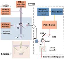
Fan Yi, Changming Yu, Yunpeng Zhang, Fuchao Liu, Yun He, Yang Yi, Zhenping Yin, and Jun Zhou
ObjectiveHigh-resolution and accurate profiles of atmospheric temperature have wide applications in weather analysis and forecasting, climate change assessment, atmospheric chemistry research, and remote-sensing measurements. Current primary tools for measuring atmospheric temperature profiles include radiosondes, microwave radiometers, and lidars. While conventional radiosondes provide temperature profiles with satisfactory accuracy and excellent height resolution, their inadequate temporal resolution (approximately 12 hours) impedes the capture of relatively rapid atmospheric processes. Temperature profiles retrieved from microwave radiometer measurements generally suffer from relatively low accuracy, as they rely on statistics-based inversion algorithms that incorporate artificially introduced assumptions. Single-line-extracted pure rotational Raman (PRR) lidar represents an active remote sensing technique capable of obtaining accurate, high-range-resolution atmospheric temperature profiles from the lower troposphere to the lower stratosphere. Originally proposed by Cooney in 1972, this concept remained unrealized for over fifty years due to technical challenges: the atmospheric pure rotational Raman spectrum consists of mixed spectral lines from nitrogen and oxygen molecules, and the bandwidth of commercially-available optical filters was excessive. Although many research teams worldwide have contributed to its development, the technical implementation was not achieved until recently. By analyzing the PRR spectra of air molecules, we identified that two individual Stokes N2 PRR lines corresponding to rotational quantum numbers J=4 and J=14 can be optically isolated using commercially available interference filters (IF) combined with Fabry-Perot interferometer (FPI). Based on this finding, we developed a single-line-extracted PRR lidar system for accurate atmospheric temperature profiling and simultaneous retrieval of aerosol/cloud backscatter coefficients.MethodsThe lidar utilizes the second harmonic (532.237 nm) of a seeded Nd∶YAG laser system with injection as an emitted light. The receiving unit comprises two different-aperture (0.3 m and 1.0 m) receivers, dedicated to near-range and far-range measurements, respectively. Each receiver is equipped with a custom-built three-channel polychromator. This advanced polychromator isolates two individual Stokes N2 PRR lines corresponding to rotational quantum numbers J=4 and J=14 (in the two Raman channels), along with the Rayleigh/Mie backscatter signal (in the elastic channel). The two Raman lines correspond to the vacuum wavelengths of 533.479 nm and 535.749 nm, respectively. Each Raman channel uses a set of signal extraction components consisting of two identical interference filters and a temperature-controlled sandwich solid Fabry-Perot interferometer. The interference filters are centered at the respective Raman wavelengths (533.479 nm or 535.749 nm), with a bandwidth of 0.16 nm, a peak transmission of approximately 60%, and an elastic-signal rejection ratio exceeding 104. The elastic channel is equipped with a single interference filter with a bandwidth of 0.3 nm and a peak transmission of about 80% at 532.237 nm.Results and DiscussionsThe atmospheric temperature T(z) has been derived from a rigorous analytical expression that relates temperature to the ratio Q(z) of the signal photon counts in the two Raman channels. This analytical expression estalishes a simple functional relation between T(z) and Q(z) involving two constant parameters, A and B. Parameter A is obtained through theoretical calculation, while B is determined via laboratory measurement, eliminating the need for external calibration using data from other instruments. Using the derived temperature profiles, aerosol and cloud backscatter coefficients can be rigorously derived from the signal photon counts in the J=4 Raman channel and the elastic channel, eliminating the need for additional assumptions such as a constant lidar ratio or ?ngstr?m relationship. This provides for the first time a valid and straightforward approach for profiling the optical properties of aerosols and clouds. The performance of the lidar system was evaluated through observational examples and statistical comparisons at a subtropical site in Wuhan, China, using an integration time of 1 hour and a vertical resolution of 150 m. During nighttime operations, the lidar effectively measured temperature profiles from approximately 2 km to 35 km in altitude. The results showed excellent agreement with simultaneous radiosonde data within the 2?16 km altitude range (the altitude range of available sonde data). The temperature measurement uncertainty in nighttime was below 1 K at altitudes up to 21 km. Under daytime conditions, the lidar successfully retrieved temperature profiles from ~2 km to 16 km, showing good consistency with simultaneous sonde data. The daytime lidar temperature profiles exhibited statistical uncertainty of less than 1 K within an altitude range from 2 to 11 km. Such a large altitude range is unprecedented for daytime lidar temperature measurements. Additionally, the pure rotational Raman lidar also demonstrated an excellent performance in revealing small-scale temperature structures, such as temperature inversions, in the troposphere.ConclusionsSingle-line-extracted pure rotational Raman lidar has been develpoed for accurate profiling of atmospheric temperature and aerosol/cloud backscatter coefficients. A seeded frequency-doubled Nd∶YAG laser is utilized as the light source. Light backscattered from atmosphere is collected by two receivers with diameters of 0.3 m and 1.0 m, respectively. Each receiver is equipped with a custom-built three-channel polychromator that isolates respectively two individual Stokes N2 PRR lines corresponding to rotational quantum numbers J=4 and J=14, along with the Rayleigh/Mie backscatter signal. The logarithm of the ratio between two PRR channel signals is a linear function of the reciprocal of atmospheric temperature. The two parameters in this function are a physical constant and a laboratory-measurable quantity, respectively. Therefore, the atmospheric temperature profiles can be obtained accurately derived from the ratio of the two PRR line signals without requiring external calibration. Based on the derived temperature profiles, the aerosol/cloud backscatter and extinction coefficient profiles can be further rigorously determined from the measured PRR J=4 signal and elastic backscatter signal, without relying on additional assumptions. The derived aerosol/cloud parameters and resulting lidar ratio provide benchmarks for aerosol and cloud lidar measurements. Field experiments have demonstrated that this lidar achieves a wide altitude coverage, high time and altitude resolutions, and unprecedented daytime performance, making it widely applicable in the fields of meteorology and atmospheric environment research.
Sep. 19, 2025Vol. 45 Issue 18 1801005 (2025)
Pan Liu, Xinhui Sun, Guangqiang Fan, Yibin Fu, Huihui Gao, Yan Xiang, Tianshu Zhang, and Wenqing Liu
ObjectiveOzone is an important trace component in the atmosphere. Stratospheric ozone can absorb ultraviolet (UV) radiation from the sun, protecting the Earth’s surface from its damaging effects. However, tropospheric ozone acts as a pollutant gas, posing health risks to human and ecosystems when concentrations are excessive. Similarly, high concentrations of ground-level aerosols not only reduce visibility but also contribute to respiratory and cardiovascular diseases. In recent years, domestic control measures for PM2.5 have led to a gradual decline in its concentrations. On the contrary, ozone pollution has become increasingly prominent. To promote the coordinated control of PM2.5 and ozone, accurate monitoring of theirspatiotemporal distribution using atmospheric lidar is essential. This enables the characterization of ozone concentrations at both local and larger scales. Achieving this goal necessitates advancements in ozone lidar laser source technology. Currently, most ozone lidar systems employ gaseous Raman laser sources, which suffer from low conversion efficiency and poor stability, rendering them unsuitable for mobile platforms such as vehicle-based monitoring. Therefore, building upon previous research, a novel compact all-solid-state free-tuning four-wavelength laser source for ozone differential absorption lidar using intra-cavity Raman laser technology has been designed. This design further enhances the stability and reliability of the laser source system. It provides a foundation for developing portable, multi-platform differential absorption lidar systems for atmospheric ozone monitoring, thereby expanding the hardware capabilities for such measurements.MethodsFor ozone detection wavelength selection, solid-state Raman media including KGW and SrWO4 crystals were systematically analyzed within an intra-cavity Raman laser system configuration. The designed laser architecture utilizes an 808 nm laser diode-pumped Nd∶YVO4 crystal to achieve dual-wavelength ultraviolet output. By implementing a nested cavity structure, the system effectively couples laser oscillation with stimulated Raman scattering within a single resonant cavity. Subsequent nonlinear optical interactions generate pulsed outputs spanning ultraviolet and visible spectral regions. This intra-cavity Raman laser serves as the emission source for ozone lidar systems, facilitating comparative atmospheric ozone detection tests to validate the laser’s operational reliability and measurement efficacy. Field validation was further conducted using both ground-based stationary and vehicle-mounted mobile monitoring platforms, enhancing regional ozone distribution monitoring capabilities.Results and DiscussionsThe implementation of an intra-cavity Raman laser system successfully generated four-wavelength laser output (Fig. 3), demonstrating superior optical performance. This laser was integrated into an ozone lidar system. Comparative validation experiments conducted at the Canton Tower environmental monitoring station (Fig. 7) confirmed the reliability and effectiveness of the intra-cavity Raman laser as the lidar emission source. Utilizing this outdoor intra-cavity Raman laser technology, the ozone lidar system performed extended ground-based observations in Xianyang city. These observations yielded high-quality detection data (Fig. 10), simultaneously capturing cloud altitude, aerosol transport and dissipation dynamics, along with spatiotemporal ozone concentration distribution patterns. Furthermore, mobile monitoring trials conducted with the lidar system in Nanjing effectively pinpointed localized ozone concentration hotspots along the survey route (Fig. 12), providing valuable technical support for tracing ozone pollution origins.ConclusionsA differential absorption lidar emission laser source for atmospheric ozone monitoring has been developed employing intra-cavity Raman laser technology. This innovative system utilizes nested resonator configurations and nonlinear optical effects to generate high-quality visible and ultraviolet laser beams, enabling simultaneous detection of atmospheric ozone and aerosol vertical profiles. The intra-cavity architecture significantly reduces reliance on external optical components, enhancing the overall system stability. Through compact integrated design, the laser’s physical dimensions have been substantially minimized, enhancing its suitablility for mobile monitoring platforms. The lidar system, based on this intra-cavity Raman laser, has been successfully deployed in multiple operational scenarios, including extended ground-based observations and vehicular mobile detection campaigns. Field monitoring data consistently demonstrate the robust and reliable system performance, establishing critical hardware foundations for advancing atmospheric ozone monitoring capabilities.
Sep. 25, 2025Vol. 45 Issue 18 1801006 (2025)
Xiaonan Zhao, Xinhui Sun, Pan Liu, Jinxin Chen, Linhao Shang, Yajun Wu, Xi Chen, Gang Cheng, Huihui Gao, Yibin Fu, Guangqiang Fan, Tianshu Zhang, and Wenqing Liu
ObjectiveOHx free radical LIDAR detection usually requires a single-frequency ultraviolet wavelength, such as 308 nm, and an optical parametric oscillator (OPO) is one of the main devices to achieve nonlinear frequency conversion. However, most traditional OPOs use wide linewidth or multi-mode lasers as pump sources, which leads to problems such as high phase noise and low spectral purity of the final output laser and limits the application of OPOs in high-precision spectral detection and quantum optics. In addition, increasing the power of single-frequency lasers faces challenges such as nonlinear effects and thermal effects in laser gain media. Therefore, it is essential to use a high-quality and high-power single-frequency pump source for pumping OPOs. In this paper, based on the efficient one-dimensional heat dissipation characteristics and spherical aberration self-compensation technology of Innoslab, we designed the Innoslab amplifier to increase the single-frequency power while keeping the beam quality unchanged, providing a good pump source for OPOs.MethodsThe thermal effect of the laser crystal is essential to the design of the Innoslab laser amplifier. We first used finite element analysis to simulate the multi-dimensional thermal effects of the laser crystal and explored the temperature distribution and thermal stress distribution of the laser crystal from each dimension. Then, we investigated whether Nd∶YVO4 would undergo thermally induced stress fracture at the theoretical pump power and determined the focal length of the thermal lens of the laser amplifier at the same theoretical pump power. Another key design factor of the Innoslab laser amplifier was the pattern matching between the seed light and the pump light. For the known pump light size, we used multiple cylindrical lenses to flexibly shape the dimensions of the seed light along the fast axis and slow axis directions to match the pump spot. In addition, while realizing the high-power single-frequency laser output, we should also avoid the deterioration of beam quality caused by the thermally induced spherical aberration effect. Therefore, we designed spherical aberration self-compensation structure based on the principle of the Fourier transform 4f imaging system.Results and DiscussionsThrough finite element analysis and simulation, the temperature distribution and multi-dimensional thermal stress distribution of the laser crystal are clarified, and the focal length of the thermal lens is further determined. We numerically determine the thermal effect of the laser crystal accurately and provide theoretical support for the design of the Innoslab laser amplifier (Fig. 3 and Fig. 4). Thermally induced spherical aberration has always been a key factor affecting the performance of Innoslab laser amplifier. The realization principle of spherical aberration self-compensation is explained from the perspective of the 4f imaging system based on Fourier optics (Fig. 5), and the beam quality before and after amplification remains the same. The design of the Innoslab laser amplifier requires that when the seed light passes through the laser crystal multiple times, its size in the fast axis direction remains unchanged, and its size in the the slow axis direction increases evenly. This purpose is achieved through the flexible design of the magnifying end-pump and multiple cylindrical lenses (Fig. 7). The engineered Innoslab laser amplifier designed has been operating continuously and stably for several months (Fig. 10).ConclusionsThe proposed high-power single-frequency laser is successfully applied to the OHx free radical LIDAR light source, and the pumped OPO module successfully outputs a 731 nm laser, which provides the basis for subsequent nonlinear frequency conversion. Compared with previous laser amplifiers, the principle of spherical aberration self-compensation is theoretically explained, ensuring that the beam quality before and after laser amplification is unchanged. In addition, the designed Innoslab laser amplifier has been applied in engineering and exhibits stability. So far, it has been operating stably for several months.
Sep. 15, 2025Vol. 45 Issue 18 1801007 (2025)
Yajun Wu, Pan Liu, Linhao Shang, Gang Cheng, Wenqing Liu, and Tianshu Zhang
ObjectiveWith the rapid and diversified development of the national economy, the current domestic atmospheric environment remains complex. So lidar is in high demand as a critical tool for monitoring air pollution and greenhouse gases. In atmospheric remote sensing lidar system, high-spectral-resolution lidar (HSRL) and differential absorption lidar (DIAL) play significant roles in fields such as atmospheric composition detection and environmental monitoring due to their high precision and high sensitivity. A high-power, narrow-linewidth, and frequency tunable 1064 nm continuous-wave (CW) single-frequency laser can be used as the light source for HSRL via pulse modulation and power amplification. It can also generate short-wave and mid-infrared lasers through nonlinear optical frequency conversion techniques such as optical parametric oscillators (OPOs), providing DIAL with rich wavelength options. This paper aims to develop a broadband, mode-hop-free, tunable CW single-frequency Nd∶YVO4 laser based on a unidirectional figure-eight ring cavity structure. In the future, this laser will be integrated as a core component into mobile-platform lidar systems, providing robust support for air pollution and greenhouse gases monitoring.MethodsIn this work, we develope a mode-hop-free, continuously tunable single-frequency laser at 1064 nm, which features a compact structure, high output power, and a broad frequency tuning range. The figure-eight ring cavity consists of four mirrors (M1?M4). M1 and M4 also serve as the pump light input and laser output couplers, respectively. The laser is pumped by a fiber-coupled laser diode. The gain medium is an Nd∶YVO4 crystal with natural birefringence. Compared to the Nd∶YAG crystal, Nd∶YVO4 has a higher absorption coefficient, a broader absorption bandwidth, and can directly generate linearly polarized lasers. To ensure single-longitudinal-mode operation, an optical unidirectional device composed of a terbium gallium garnet (TGG) crystal and a half-wave plate (HWP) is added into the cavity to eliminate the spatial hole burning. To achieve high power output, an etalon with a free spectral range (FSR) much larger than the cavity’s FSR is incorporated to narrow the effective gain bandwidth and suppress competing longitudinal modes. Intracavity insertion of a noncritically phase-matched LiB3O5 (LBO) crystal enables 532 nm laser output, which coincides with the absorption line of iodine molecules, facilitating long-term frequency stabilization. Finally, through coordinated control of the laser crystal temperature and piezoelectric ceramics (PZT)-driven cavity mirror, continuous mode-hop-free frequency tuning over a range of 14 GHz is achieved.Results and DiscussionsExperimental results demonstrate that the laser designed in this work exhibits excellent performance in all aspects. Under a pump power of 25 W, the maximum output powers of the fundamental-wave and second-harmonic-wave laser reach 6.5 W and 2.1 W, with slope efficiencies of 26.12% and 8.36%, respectively (Fig. 4). The power stabilities over 4 h are 0.23% and 0.31% (Fig. 5). Within 1.35 h, the fundamental-wave power fluctuation is approximately ±0.238 pm (±63.1 MHz) (Fig. 7). The PZT tuning coefficient of the fundamental-wave is about -0.58 pm/V (-153.53 MHz/V) (Fig. 8), while the temperature tuning coefficient is about -26.89 pm/℃ (-7.12 GHz/℃) (Fig. 9). By employing the coordinated control of crystal temperature and cavity length, mode-hop-free wavelength tuning over a range of 53.16 pm (14.08 GHz) is achieved (Fig. 10). Compared to the method of coordinated control of the etalon angle and PZT-driven mirror, the wavelength tuning approach proposed in this paper eliminates the need for complex mechanical and electronic control systems. Although the experimental results align well with theoretical predictions, the current frequency tuning method requires further refinement. Due to the inherent thermal inertia of crystal temperature adjustment, the tuning speed must remain moderate, and nonlinearity is observed during the initial and final stages of frequency tuning (Fig. 10). Additionally, hysteresis effects in the PZT actuator introduce deviations in wavelength tuning linearity. These issues will be systematically addressed in future work.ConclusionsThis paper presents a continuous-wave single-frequency Nd∶YVO4 laser based on a figure-eight ring cavity, achieving 6.5 W of fundamental-wave and 2.1 W of second-harmonic wave laser output, with power stabilities of 0.23% and 0.31% over 4 h, respectively. Continuous wavelength tuning across a 14 GHz range is achieved by driving a PZT mounted cavity mirror to adjust the resonator length while synchronizing with laser mode variations induced by crystal temperature tuning. This laser overcomes the limitations of conventional cavity length control methods, which only allow continuous tuning within a single longitudinal mode. And, in contrast to approaches that require coordinated control of the etalon angle and cavity length, our design eliminates the need for complex control systems involving galvanometer actuators and phase-locked electronics. However, its tuning range and speed are still inferior to what can be achieved with etalon angle control, and further improvements are needed for the linearity of the control algorithm. Finally, the wavelength tuning performance is experimentally verified by scanning the absorption spectrum of iodine molecules. Potential applications of this laser include lidar systems or serving as a pump source for mid-infrared OPOs.
Sep. 03, 2025Vol. 45 Issue 18 1801008 (2025)
Yinan Wang, Wei Zhao, Yubing Pan, Yinghua Qiu, and Daren Lu
ObjectiveMultiwavelength lidar aerosol microphysical parameter retrieval represents a fundamental ill-posed inverse problem governed by Fredholm integral equations, where limited optical observations must constrain infinite-dimensional particle size distributions. Current regularization methods provide only point estimates without uncertainty quantification, severely limiting their applications in climate model validation and data assimilation. The IPCC sixth assessment report identifies aerosol-radiation interactions as the largest uncertainty source in climate forcing (-2.0~-0.4 W·m-2), largely due to inadequate aerosol property characterization. Traditional approaches suffer from three critical limitations: subjective regularization parameter selection, absence of uncertainty bounds, and inability to systematically incorporate prior physical knowledge. This study develops a comprehensive Bayesian framework that transforms deterministic retrieval into probabilistic inference, providing rigorous uncertainty quantification essential for advancing atmospheric aerosol science and climate applications.MethodsWe establish a complete Bayesian inversion framework based on Mie scattering theory: gp(λ)=∫Kp(λ, r, m)v(r)dr+ε, where gp(λ) represents observed optical parameters, Kp(λ, r, m) is the Mie-derived kernel function, v(r) is volume size distribution, and ε denotes measurement noise. The continuous distribution is discretized using eight B-spline basis functions with weight coefficients w treated as random variables. The hierarchical Bayesian model specifies P(w|α)=N(0, α-1I) and P(g|w, A, β)=N(Aw, β-1I), where precision hyperparameters α and β follow Gamma priors and are automatically estimated through variational inference. This eliminates subjective parameter selection while providing complete posterior distributions P(w|g, A)=N(μw, Σw) with mean μw=(αI+βATA)-1βATg and covariance Σw=(αI+βATA)-1. We rigorously establish mathematical equivalence between Tikhonov regularization and Bayesian maximum a posteriori (MAP) estimation, demonstrating that classical methods emerge as special cases of our probabilistic framework, thus providing unified theoretical guidance for method selection.Results and DiscussionsComprehensive validation using 3β+2α lidar configurations (355, 532, 1064 nm backscatter; 355, 532 nm extinction) demonstrates exceptional performance across challenging scenarios. For bimodal distributions representing atmospheric fine and accumulation modes, geometric mean radius retrieval errors remain below 5% (fine mode: -0.6%, accumulation mode: +4.4%) with effective radius errors under 3.5% (Fig. 3). Under realistic noise conditions (10%?20%), the Bayesian method exhibits superior robustness through automatic regularization adaptation, while posterior variance analysis reveals physically meaningful uncertainty patterns: elevated uncertainty in modal boundaries (0.2?0.4 μm) reflecting observational constraints, and high uncertainty in large particle tails consistent with reduced lidar sensitivity (Fig. 4). Statistical validation through 1000 Monte Carlo experiments confirms 95% credible intervals, demonstrating accurate uncertainty quantification. The method correctly captures aerosol microphysics where fine particles dominate numerically (90.9%) while accumulation mode controls volume (93.5%) and optical properties. Comparative analysis reveals complementary characteristics: Tikhonov excels in computational efficiency and single-mode accuracy (1.24% mean error), while Bayesian provides comprehensive uncertainty information with comparable accuracy (2.29% mean error), making it optimal for scientific applications requiring rigorous uncertainty assessment.ConclusionsThis paper establishes a transformative Bayesian framework for multiwavelength lidar aerosol retrieval that addresses fundamental limitations of deterministic approaches. Key contributions include: 1) complete probabilistic formulation providing both accurate retrievals and comprehensive uncertainty quantification; 2) rigorous mathematical unification of regularization methods under Bayesian theory; 3) automatic hyperparameter estimation eliminating subjective parameter selection; 4) demonstrated superior robustness and statistically validated uncertainty bounds. The framework’s scientific impact extends to climate model evaluation through quantified parameter uncertainties, improved data assimilation via observation error covariances, and uncertainty-aware environmental monitoring. Experimental validation confirms geometric mean errors below 5% with reliable uncertainty propagation under observational noise. This probabilistic paradigm represents a significant methodological advancement for atmospheric remote sensing, providing essential tools for climate prediction, air quality assessment, and environmental policy applications requiring rigorous uncertainty quantification.
Sep. 19, 2025Vol. 45 Issue 18 1801009 (2025)
Chao Ban, Weilin Pan, Zhaonan Cai, Wentao Huang, and Rui Wang
ObjectiveThe middle atmosphere, extending from the stratosphere to the lower thermosphere, functions as a critical transitional region between the lower and upper atmosphere. This layer exhibits complex dynamical processes—including gravity waves, atmospheric tides, and planetary waves—that substantially influence global circulation, energy transport, and vertical coupling across atmospheric layers. Precise characterization of these processes necessitates high-resolution temperature measurements, obtainable through Rayleigh scattering Lidar systems. These Lidars detect molecular backscatter signals, enabling accurate temperature profiling of the middle atmosphere with fine spatial and temporal resolution. Two principal methods are commonly employed to retrieve temperature profiles from Rayleigh Lidar measurements: the hydrostatic equilibrium method developed by Hauchecorne and Chanin (HC, also referred to as the C-H method), and the optimal estimation method (OEM). The HC method, a classical approach, utilizes hydrostatic equilibrium and integrates downward from a specified reference temperature at a high altitude. Although widely implemented, its accuracy depends significantly on the selected reference point. Conversely, OEM is a statistical retrieval method based on Bayesian theory. It integrates observational data with prior information to minimize uncertainties and enhance retrieval stability, proving particularly effective for nonlinear and ill-posed inverse problems. This study conducts a systematic comparison of the HC and OEM methods using both simulated and actual Lidar observations from Zhongshan Station, Antarctica. Their performance is assessed regarding retrieval accuracy, error propagation, and sensitivity to reference conditions, thus providing insights into Rayleigh Lidar retrieval method optimization.MethodsSimulations were based on Rayleigh Lidar observations collected at Zhongshan Station on August 10, 2020. A synthetic Lidar signal was constructed using temperature profiles from the CIRA-86 model, which served as the true reference temperature. Temperature retrievals were then performed using both the HC and OEM methods. The HC method primarily relies on the hydrostatic equilibrium equation and the ideal gas law. An altitude was selected as the reference height where the uncertainty in the retrieved atmospheric density is 10%, and the corresponding model temperature at this altitude was used as the reference temperature. The OEM is based on Bayesian statistical theory and implemented using a least-squares optimization framework. Its fundamental principle involves the weighted integration of observational data and prior knowledge (such as the prior state vector and its covariance) in the error covariance space, thereby deriving the most physically reasonable state estimate that optimally fits the actual observations. In the application of the OEM, a suitable forward model [equation (14)] was constructed based on the Rayleigh Lidar equation, and the MSISE-00 model temperature was used as the a priori temperature profile.Results and DiscussionsTemperature retrievals using both HC and OEM methods were evaluated with the simulated lidar signals. The HC method, based on hydrostatic equilibrium, effectively retrieved the temperature structure across most of the vertical range when accurate reference temperatures were available (Fig. 2). However, the method exhibited high sensitivity to the chosen reference temperature, particularly within the 10?15 km region below the reference height where retrieval uncertainties increased substantially (Fig. 3). The OEM, evaluated through its averaging kernel matrix, demonstrated that observational data dominated the retrieval below 96 km (Fig. 5), while error budget analysis (Fig. 7) systematically quantified contributions from observation noise, forward model errors, and prior information. Additionally, the OEM’s enhanced robustness was confirmed through reference pressure perturbation tests (Fig. 8), demonstrating significant stability against such variations. Validation using actual Lidar measurements revealed good agreement between the two methods. Temperature differences remained generally below 2% below 87 km (Fig. 9), indicating consistency between the HC and OEM retrievals under well-constrained conditions.ConclusionsIn the present study, we compare HC and OEM temperature retrieval methods using Rayleigh Lidar signal from Zhongshan Station, Antarctica, and CIRA-86-based simulations. Key findings include: 1) both methods achieved accurate retrievals below 95 km with true reference parameters, with the HC method showing slightly better precision; 2) HC method exhibited strong sensitivity to reference temperature (especially within 10?15 km below the reference height), while OEM demonstrated superior robustness against reference pressure perturbations; 3) OEM enabled comprehensive uncertainty quantification (observation noise, model errors, etc.), offering distinct advantages for scientific analysis; 4) the HC method, due to its simplicity and low computational cost, remains well suited for operational or real-time applications. While both methods can reliably retrieve atmospheric temperature profiles, OEM is better suited for scientific applications requiring comprehensive uncertainty quantification, whereas the HC method is more applicable in scenarios prioritizing algorithmic simplicity and retrieval stability.
Sep. 12, 2025Vol. 45 Issue 18 1801010 (2025)
Kahou Nong, Wei Gong, Yingying Ma, Yun He, Zhenping Yin, Detlef Müller, Huijia Shen, Qiaoyun Hu, and Igor Veselovskii
ObjectiveCirrus clouds, consisting entirely of ice crystals in the upper troposphere, cover approximately 25% of the globe at any given time. These clouds produce a net warming effect through substantial longwave trapping, despite reflecting some solar radiation. Ice crystal formation occurs through two pathways: homogeneous nucleation, which requires temperatures below -38 ℃ and high ice supersaturation, or heterogeneous nucleation on ice-nucleating particles (INPs) such as mineral dust and smoke at lower supersaturation levels. These distinct formation mechanisms result in different microphysical properties: heterogeneous nucleation typically produces fewer, larger crystals and optically thinner clouds, while homogeneous nucleation generates numerous small crystals that enhance infrared heating. Although the upper troposphere above oceanic regions is generally considered pristine, Asian dust transported over long distances can reach altitudes of 5?15 km and periodically seed cirrus formation in remote areas, including the mid-North Atlantic. However, the quantitative impact of such transported dust on ice formation—and consequently on cirrus radiative forcing—remains inadequately understood due to limited direct in-situ observations. This study examines representative oceanic cases to determine the relative prevalence of heterogeneous versus homogeneous nucleation in dust-influenced cirrus, providing essential constraints for climate models and reducing uncertainty in cirrus feedbacks.MethodsIn this study, we first interrogate CALIPSO/CALIOP profiles to locate dust?cirrus co-occurrences along the trans-Pacific/North American corridor into the North Atlantic. We use CALIOP Level-1 (v4.51) 532 nm attenuated backscatter and volume depolarization ratio to flag layered features, and Level-2 aerosol profiles (v4.2) to obtain extinction, particle depolarization, and the vertical feature mask for subtype identification (pure/polluted dust and cirrus). Because automated classification can confuse optically thin cirrus with dust, we apply additional screening based on depolarization thresholds and layer continuity, and collocate meteorology (temperature, pressure, relative humidity) from embedded MERRA-2 fields. To characterize cirrus microphysics, we use A-Train DARDAR products that combine CloudSat CPR with CALIOP. DARDAR-Cloud provides extinction, effective radius, and ice water density; DARDAR-Nice supplies ice crystal number concentration (ICNC) profiles for ice crystal diameters greater than 5, 25, and 100 μm at 60 m vertical and 1.7 km horizontal resolution. Recognizing lidar?radar size-sensitivity differences and known retrieval limitations, we assign a conservative factor-of-three uncertainty to ICNC. Dust-related ice-nucleating particles concentration (INPC) is derived with POLIPHON using dust extinction as input. Dust extinction is separated from total aerosol extinction via a one-step method and computed assuming a dust lidar ratio of 45 sr. We convert extinction to dust mass, coarse-mode number, and surface area concentrations with regionally constrained coefficients from nearby AERONET observations (Tudor Hill). Given the very low cirrus temperatures, we restrict nucleation to deposition mode and calculate INPC with the U17-D parameterization using dust surface area as predictor. We define dust?cirrus interaction when vertical or horizontal overlap is evident. Event provenance is corroborated with daily MERRA-2 dust column mass fields and HYSPLIT back-trajectories (GDAS-driven), linking the observed North Atlantic layers to Asian sources and establishing two rare, long-range transport cases for subsequent INPC?ICNC closure.Results and DiscussionsIn the first event (May 18, 2007), CALIOP reveals a cirrostratus deck embedded within a pure dust layer between 9.4 and 10.9 km, exhibiting strong attenuated backscatter and high depolarization that indicate nonspherical ice and dust (Fig. 1). HYSPLIT traces the air mass to Asian deserts on May 9?10, with elevated layers tracked across the Pacific, over North America, and into the North Atlantic (Figs. 2?3). Within the overlap zone, DARDAR-Cloud retrievals demonstrate mean extinction near 0.10 km-1, an effective radius of 39.2 μm, and an ice water density of 2.0 mg·m-3 (Fig. 4). Using POLIPHON-derived dust extinction with the U17-D scheme, the dust INPCs measure 26.0 L-1 at an ice saturation ratio of 1.15 and 483.5 L-1 at 1.25, increasing toward the cloud top (Fig. 5). Collocated DARDAR-Nice indicates mean ICNCs of 32.3 L-1 for diameters larger than 5 μm, 15.3 L-1 for larger than 25 μm, and 2.4 L-1 for larger than 100 μm, peaking approximately 0.3 km below the top (Fig. 5). Excluding the 1.25 case—where dust INPC exceeds ICNC, likely due to sedimentation and particle-size assumptions—the closure remains within one order of magnitude, supporting dust-driven heterogeneous nucleation. In the second event (April 25, 2008), a smaller cirrus system between 10.0 and 11.4 km exists adjacent to a polluted or aged dust layer. The aerosol exhibits weaker backscatter and lower volume depolarization ratio (0.1?0.2), while the cirrus maintains higher volume depolarization ratio above 0.3 (Fig. 6). Trajectories again suggest Asian sources and sustained lofted transport between roughly 7 and 11 km (Figs. 7?8). Microphysical retrievals indicate mean extinction near 0.25 km-1, an effective radius of 56.9 μm, and an ice water density of 8.9 mg·m?3 (Fig. 9). Under temperatures of -54 to -57 ℃ and typical ice saturation ratios of 1.15?1.25, the U17-D scheme, reduced tenfold to reflect aging, yields mean dust INPC from 4.4 to 95.7 L-1 (Fig. 10). The corresponding ICNC averages are 68.9 L-1 (>5 μm), 34.1 L-1 (>25 μm), and 6.6 L-1 (>100 μm), with localized enhancements in nice,5 μm approaching 500 L-1 (Figs.9?10). The near-closure again indicates heterogeneous nucleation dominance; brief high-ICNC pockets likely reflect transient updrafts or partial INP depletion. These two trans-Pacific cases demonstrate that Asian dust maintains ice-nucleating activity after extensive transport and can significantly influence cirrus formation over the North Atlantic, with pure dust active at lower saturation and polluted dust requiring slightly higher saturation to produce comparable ice.ConclusionsTo reduce uncertainties in cloud radiative forcing and climate projections, models must explicitly represent how Asian dust is lofted by midlatitude westerlies, traverses the Pacific, and enters the North Atlantic, while maintaining ice-nucleation activity after long-range transport. Clay minerals such as kaolinite and illite provide efficient ice-nucleating sites at relatively warmer upper-tropospheric temperatures, increasing initial ice crystal numbers, shifting sizes toward larger particles, rapidly consuming supersaturation, and inhibiting subsequent homogeneous freezing. These modifications affect cirrus effective radius, ice water density, and the balance between longwave cooling and shortwave reflection, potentially influencing regional heat budgets and circulation. Therefore, global and regional models should incorporate prognostic dust mineralogy and aging-dependent INP efficiency, resolve competition between heterogeneous and homogeneous pathways under realistic updrafts, and evaluate against combined lidar?radar constraints (e.g., CALIPSO/CloudSat and EarthCARE) and reanalysis dust fields. Additional marine INP sources (sea salt, smoke, volcanic aerosols) should also be considered. Our North Atlantic cases demonstrate that dust-driven heterogeneous nucleation can dominate cirrus formation, emphasizing the importance of including these processes to reduce radiative-forcing uncertainty.
Sep. 19, 2025Vol. 45 Issue 18 1801011 (2025)
Minjie Zhao, Fuqi Si, Haijin Zhou, Yu Jiang, and Lei Zhu
ObjectiveOxygen A-band (O2A, 762 nm) airglow is one of the strongest radiation features in the middle and upper atmosphere. O2A airglow is evenly distributed across all latitudes and occurs at altitudes of 40‒200 km. Most ground-based measurements are limited due to the strong absorption of O2 in the airglow. Therefore, it is necessary to study space-based limb detection methods to detect global airglow. Based on this, the global temperature profile can be obtained. This profile supports studies of atmospheric environmental change, atmospheric dynamics, and meteorological monitoring.MethodsUsing the temperature and ozone profile monitoring spectrometer (TOPS), we discuss space-based limb detection methods for O2A airglow. TOPS was launched on January 29, 2025, to measure the global distribution of temperature, atmospheric ozone, and other atmospheric components. In this paper, the O2A airglow radiation calculation method is analyzed. Using TOPS’s limb observation geometry, along with temperature, pressure, oxygen number density in each layer, and O2 self-absorption data, we calculate high-spectral-resolution airglow emissions at different limb tangent heights. Then, TOPS’s detection mode and system parameters are analyzed, and spectral and radiometric calibrations are performed to obtain TOPS’s performance parameters. Next, the on-orbit airglow data detected by TOPS are preprocessed, and the optimal estimation algorithm is used to retrieve the temperature profile. We also discuss the selection method of the inversion wavelength. O2A airglow lines are generally classified as strong, medium, or weak. The inversion wavelength is selected by analyzing each line’s radiation intensity, atmospheric transmittance, and temperature dependence. Finally, for an error analysis, the random noise error, smoothing error, and model error of the inversion results are discussed.Results and DiscussionsIn the O2A airglow radiation calculation, the pressure, temperature, and O2 number density profiles are obtained from the MISI model, and the O2 line intensity is obtained from the HITRAN database. We obtain the high spectral resolution O2A airglow radiation from 60 to 100 km (Fig. 5). The results show that airglow radiation varies with tangent height, primarily due to changes in excited oxygen number density and O2 self-absorption. The results also show a strong oxygen self-absorption effect at the tangent height of 60 km, and the effect decreases with increasing height. Due to the low emission intensity, TOPS adopts a limb scanning mode, with an instantaneous field of view of 200 km (horizontal)×2 km (vertical), a vertical scanning range of 10‒100 km, and a vertical resolution of 2 km (Fig. 6 and Fig. 7). TOPS’S spectral range is 498.1‒802.3 nm, spectral resolution is 1.46 nm, spectral calibration accuracy is 0.1 nm, and radiometric calibration accuracy is 3.6%. The signal-to-noise ratio is 140 at a tangent height of 80 km. Analysis results show that TOPS can accurately detect O2A airglow. The in-orbit O2A airglow data detected by TOPS are preprocessed, providing knowledge of the dependence of O2A airglow radiation on tangent heights and solar zenith angles. Based on TOPS’s spectral resolution, we use the optimal estimation algorithm to invert the temperature profile. For the inversion wavelength selection, the weak lines have a strong positive response to temperature increases, while the strong lines are difficult to use for recovering temperatures at lower altitudes due to strong self-absorption. Combined with the spectral resolution of TOPS, the medium line at 765 nm is selected. The inversion results show that the average kernel function peak above 80 km is more than 0.6. As self-absorption increases, the average kernel function peak decreases to less than 0.1 below 80 km, indicating that the temperature inversion error increases. At the same time, it can also be seen that the weight function peak above 90 km and below 75 km decreases, but the average kernel function peak above 90 km basically does not decrease, indicating that the inversion accuracy in the region above 90 km is higher than that in the region below 75 km (Fig. 14). The error results show that errors above 80 km mainly come from measurement errors, whereas errors below 80 km mainly come from the temperature prior due to the significant contribution of the prior values to the inversion results. The error range is -6 to 6 K at 90‒100 km, -10 to 10 K at 80‒90 km, and -12 to 12 K at 64‒80 km.ConclusionsThe analysis of in-orbit airglow shows that TOPS can detect O2A airglow effectively. The limb detection method, system, and performance parameters of TOPS serve as a reference for designing systems to monitor the middle and upper atmosphere. Based on O2A airglow spectra, we initially obtain the temperature profile using the optimal estimation algorithm. This provides a foundation for analyzing long-period airglow data, optimizing inversion algorithms, and cross-comparing inversion results.
Sep. 18, 2025Vol. 45 Issue 18 1801012 (2025)
Haiyan Luo, Wei Xiong, Zhiwei Li, and Hailiang Shi
ObjectiveThe accurate detection of near-space (20?100 km) atmospheric density profiles plays a pivotal role in spacecraft orbit optimization, aircraft thermodynamic performance evaluation, and space environment monitoring. Nevertheless, conventional optical remote sensing techniques are limited by constraints such as low light flux, inadequate spectral resolution, and coarse vertical sampling intervals, which pose significant challenges to the detection of fine-scale structures associated with key dynamic processes. Aiming at the demand for space-borne high-precision detection of near-space atmospheric density profiles, optical design and performance verification of hyperspectral atmospheric density profile imager (HDI) are conducted. Using single frame limb observation image by HDI, high-spatial-resolution hyperspectral information of oxygen A-band absorption spectrum and airglow radiation spectrum can be acquired over an atmospheric vertical height range of approximately 100 km, while simultaneously inverting atmospheric density profiles and temperature profiles.MethodsBased on the principle of spatial heterodyne interferometric imaging spectroscopy (SHIS), the HDI optical system is designed. It can meet the high-precision detection requirements for near-space atmospheric density profiles, which include high signal-to-noise ratio (greater than 100 under typical spectral radiance), hyperspectral resolution (better than 0.04 nm), and fine vertical sampling interval (better than 0.1 km).To meet the technical index requirements of HDI, relationships between basic parameters of each functional component and residual polarization sensitivity characteristics of HDI are analyzed, and the optimized design of the optical system is completed. The optical system includes a front component with orthogonal heterogeneous optical field modulation, a spatial heterodyne interferometer, and a re-imaging component. The front component consists of a front cylindrical lens and a collimator lens. The front cylindrical lens group has a focal length of 534.5 mm, a spectral field of view of ±1.85°, and corresponds to a horizontal atmospheric width of 160 km. The front collimator lens group has a focal length of 461.6 mm, a spatial field of view of ±1.185°, and corresponds to a vertical atmospheric height range of 102 km. Consequently, the sampling resolution interval of HDI in the spatial dimension is approximately 0.1 km.In spatial heterodyne interferometric spectrometers, there are various polarization-sensitive components such as diffraction gratings, mirrors, and beam-splitting prisms. When the optical system itself exhibits residual polarization sensitivity, it not only impairs the radiometric measurement accuracy of the spectrometer but also leads to image separation in imaging spectrometers. The HDI polarization response model and measurement platform are established. Test results indicate that by incorporating a quartz wedge-type depolarizer between the field diaphragm of the front cylindrical lens group and the mirror in the HDI optical system, and adjusting the depolarizer to ensure the maximum image separation occurs in the spectral dimension, the influence of the depolarizer on the spatial dimension imaging quality and reconstructed spectral accuracy of HDI can be minimized.Results and DiscussionsGround tests and calibration results confirm that HDI meets all design specifications. Spectral characterization shows an operational range of 756.8?771.4 nm, which fully covers the primary absorption region of the oxygen A-band (759?769 nm). Calibration with tunable laser and wave-meter yields a measured spectral resolution of 0.0394 nm, which is in close agreement with theoretical predictions. Under typical entrance pupil radiance, during limb observation at an orbital altitude of 520 km, with spatial binning of 20 pixel in the atmospheric vertical direction (corresponding to a vertical profile spatial resolution of 2 km), the average spectral signal-to-noise ratio (SNR) is 149. However, due to the detector heat sink cooling temperature of -16.2 ℃, which is slightly higher than the designed value of -20 ℃, the dark current noise of HDI in orbit has increased marginally. Consequently, the average spectral SNR of HDI is slightly lower than 149, but it still satisfies the requirement (≥100).ConclusionsThe development of HDI makes a significant advancement in space-borne hyperspectral detection of near-space atmospheric parameters. These technical achievements not only provide critical data support for current aerospace atmospheric monitoring missions but also lay a foundation for long-term global atmospheric density profile remote sensing.To meet the requirements of data applications, a variable-scale data binning processing method will be adopted in the future to retrieve high-precision atmospheric density profile data products. Additionally, to accurately assess the on-orbit spectral resolution of HDI and its capability for airglow spectrum in the middle and upper atmospheres, it is planned to reconfigure the on-orbit operating parameters of HDI. This reconfiguration aims to detect and analyze the hyperspectral characteristics of atmospheric tracers at altitudes above 80 km, while also conducting research on the retrieval of atmospheric temperature profiles in the near-space region (80?110 km).
Sep. 03, 2025Vol. 45 Issue 18 1801013 (2025)
Zhensong Hu, Jiachang Zhang, Lianqing Dong, and Yun Su
SignificanceThe construction of large space telescopes involves substantial costs. However, the rapid advancement of small satellite and CubeSat technologies has introduced a new era of low-cost, highly flexible small space telescopes. Currently, the only large ultraviolet (UV) telescope in orbit, the Hubble Space Telescope, faces deteriorating UV instruments. Meanwhile, next-generation UV telescopes, such as the U.S. Habitable Worlds Observatory and Russia’s Spektr-UV, are not scheduled for launch until after 2030. This gap presents an optimal opportunity for developing small UV telescopes to observe valuable scientific targets.ProgressSince 2020, NASA has initiated dedicated funding programs for space astrophysics satellites, including the Astrophysics Pioneers program (supporting missions with lifecycle costs of 10?20 million dollars) and CubeSat initiative (below 10 million). These programs have generated several specialized UV small satellite projects, such as the Colorado Ultraviolet Transit Experiment (CUTE), Europa Ultraviolet Spectrograph (Europa-UVS), Star-Planet Activity Research CubeSat (SPARCS), and Apsera. Notably, mid-sized countries have gained opportunities to independently develop their own small satellites. For instance, Czech Republic has led its own astronomy program, Quick Ultra-Violet Kilonova Surveyor (QUVIK). Based on their scientific objectives, these missions can be categorized into three groups: exoplanet-focused missions (CUTE and Europa-UVS), stellar activity monitors (SPARCS and QUVIK), and diffuse source mappers (Aspera).CUTE, the first ultraviolet CubeSat mission dedicated to exoplanetary atmosphere observations, was funded by NASA’s Pioneers Program, with a total lifecycle cost of $16 million. Its primary scientific objective is to quantify atmospheric escape from hot Jupiters through near-UV spectra in a bandpass of 247.9?330.6 nm, specifically targeting Mg I (285.2 nm) and Fe II (240?260 nm) absorption features during exoplanetary transits. To achieve high-resolution observations of ultraviolet spectral lines while conforming to the constrained 4U volume, CUTE utilizes a 6U CubeSat platform housing a compact Cassegrain telescope paired with a holographic grating (Fig. 1). CUTE implements a “point-stare-repeat” observation strategy, wherein the spacecraft repeatedly revisits the same exoplanet over a 4?8 week observation window. Launched in 2021, CUTE has successfully obtained a series of observational datasets (Fig. 2), including the ultraviolet spectra of the exoplanet WASP-189.Europa-UVS, as a critical subsystem of NASA’s flagship Europa Clipper mission, aims to investigate the habitability of Europa. Europa, a prime candidate for harboring a subsurface ocean, exhibits water vapor plumes and atmospheric outgassing detectable in the far-UV waveband. Europa-UVS systematically examines these phenomena through three observational modes: 1) push-broom imaging during close flybys; 2) disk-scanning from large distance through the airglow port; 3) measuring trace elements during solar occultation. Europa-UVS employs a 15-cm Rowland circle spectrograph (55?206 nm) with an effective area of 4 cm×4 cm. Its advanced microchannel plate (MCP) detectors have atomic-layer-deposited MgF2 photocathodes, which enable high-sensitivity measurements in the radiation-heavy Jovian environment (Fig. 3).SPARCS is an ultraviolet microsatellite mission led by the University of Arizona. It received funding from NASA’s 2016 Astrophysics Research and Analysis Program. Targeting nearby M-dwarf stars (10%?60% solar mass), it examines their intense, variable UV radiation that drives atmospheric photochemistry in orbiting planets, affecting key molecules like water and ozone. SPARCS operates in two UV bands: the near-UV band centers on the 280 nm Mg II line, primarily tracing the stellar chromosphere, while the far-UV band includes C IV and He II lines, originating from the transition region between the chromosphere and corona. SPARCS is a 6U CubeSat and has a mass of ~12 kg. This satellite employs a 9 cm aperture, RC telescope paired with a 1000×1000 CCD detector (Fig. 4). To minimize data transmission volume, SPARCS implements a “stamp imaging” strategy, which involves extracting only 10 pixel×10 pixel regions around targets, reducing daily science data downlink to less than 120 MB.QUVIK is the first Czech-led ultraviolet telescope, developed by Masaryk University and partners. It aims to study kilonovae from neutron star mergers by capturing early ultraviolet emissions, helping distinguish explosion mechanisms. QUVIK has a 1°×1° field of view and two channels: far-UV (140?190 nm) and near-UV (260?360 nm), enabling analysis of ejecta structure based on two wavebands. Its optical system utilizes an RC design with corrective lenses, splitting light via a dichroic mirror onto two 4096 pixel×4096 pixel detectors. QUVIK employs a rapid-response mode—when a merger is detected, it reorients within 20 minutes to observe early emissions, providing critical UV data for astrophysical studies.Apsera, an EUV small satellite mission led by the University of Arizona, represents one of the initial projects funded under NASA’s 2020 Astrophysics Pioneers Program. The mission’s primary objective is to detect warm-hot phase plasma gas in the halos of nearby galaxies and map its two-dimensional distribution. Drawing upon the technical heritage of the FUSE ultraviolet telescope, Apsera utilizes four parallel-channel Rowland-circle spectrometers within a single payload, though in a more compact configuration. Each spectrometer incorporates an off-axis parabolic primary mirror (6.2 cm×3.7 cm aperture) and a toroidal diffraction grating. To enhance observations of faint, extended sources, Apsera implements strategic improvements: balancing slightly lower spectral resolution (R>1500) with increased sensitivity to diffuse emissions (Fig. 5).Given that China’s technological expertise in ultraviolet space telescopes predominantly centers on imagers, imaging technology and associated scientific objectives are anticipated to be the initial areas of advancement. The scientific scope can extend from solar observations to other stellar objects, such as SPARCS observing M dwarfs or QUVIK observing kilonovae, both utilizing imaging systems.Conclusions and ProspectsThis paper systematically reviews the scientific objectives and technical approaches of small UV telescopes, aiming to provide strategic references for China’s future planning and development of ultraviolet small satellites missions.
Sep. 15, 2025Vol. 45 Issue 18 1828001 (2025)
Ping Zhu, Huizeng Liu, Hong Qiu, Mi Song, Xiuqing Hu, and Peng Zhang
SignificanceIn a stable climate system, there is a fundamental balance between the solar radiation energy reaching the Earth and the reflected shortwave solar radiation and emitted longwave radiation energy leaving the Earth. The transfer of radiative energy within the Earth-atmosphere-ocean system is a complex dynamic process. Remote sensing of Earth’s radiation budget (ERB) from space is the most effective way to monitor the climate system’s radiative energy balance, verify progress toward global carbon sinks and carbon neutrality, and track large-scale climate changes. Achieving these goals requires precise, continuous, quantitative remote sensing of incoming solar radiation, reflected shortwave radiation, and emitted longwave radiation from multiple locations outside Earth’s atmosphere. Human activities can significantly alter surface albedo and atmospheric composition. Changes in surface albedo directly affect the absorption of shortwave radiation, while the increase in atmospheric greenhouse gases enhances the greenhouse effect, hindering the escape of longwave radiation energy. Most of this energy remains trapped in the atmosphere and hydrosphere, disrupting Earth’s radiative energy balance. The longwave and shortwave radiation measurements help quantify Earth’s radiation energy imbalance (EEI), with an average of 0.50?1.00 W/m2 from 2005 to 2025, derived from satellite-based observations and ocean heat content measurements, and are associated with unprecedented warming in the 21st century. This imbalance, driven by increased greenhouse gases trapping longwave radiation, results in over 90% of excess heat being absorbed by oceans, exacerbating sea-level rise and extreme weather events. By continuously improving the accuracy of instrument observations and calibration, and optimizing algorithms for multi-source data analysis and fusion, the future direction of Earth’s radiation budget remote sensing lies in advancing spatiotemporally continuous monitoring of the true magnitude of Earth’s radiation energy imbalance from outside the atmosphere. Furthermore, ERB data shed light on the roles of clouds and aerosols. Clouds can cool the planet by reflecting sunlight or warm it by trapping heat, with their net effect depending on type and structure. Aerosols act as cloud condensation nuclei, influencing precipitation and radiation scattering. In essence, space measurements validate models, detect trends, and inform policy on climate mitigation. As of 2025, ongoing data from CERES and emerging satellites underscore ERB’s role in addressing global warming, emphasizing the need for sustained orbital monitoring to safeguard Earth’s habitability.ProgressThe Clouds and the Earth’s Radiant Energy System (CERES) offers the longest continuous record of outgoing longwave and reflected shortwave radiation. However, achieving complete global spatial sampling of Earth’s diurnal cycle remains a challenge. This typically requires combining geostationary satellite data, which interpolates the 24-h cycle, with polar-orbiting satellite data to derive a global Earth’s radiation energy imbalance. To address these limitations, the Space Science Center at the Institute for Advanced Study, Shenzhen University, is leading a pathfinder ERB experiment that will monitor outgoing longwave and reflected shortwave radiation using the Chang’e-7 lunar orbiter. The experiment will test the feasibility of monitoring Earth’s radiation budget from the Moon. If successful, Moon-based ERB measurements could provide a stable, long-term, highly accurate platform for global climate monitoring, overcoming traditional satellite limitations and greatly improving our understanding of Earth’s radiation energy imbalance. The Moon-based ERB (MERB) experiment is an international collaboration, with Dr. Mustapha Meftah and Dr. Alain Sarkissian from UVSQ/LATMOS contributing to instrument validation, calibration, characterization, and scientific data analysis. The MERB flight model is being ground-calibrated in a traceable radiometry laboratory at Shenzhen University. A 2.2-m-diameter, 2.0-m-long vacuum chamber is being set up within a Class 1000 cleanroom. This chamber integrates a Sun simulator, a deep-space background radiation blackbody, a terrestrial longwave radiation blackbody, and an integrating sphere light source with eight distinct wavelength bands. The spectral and radiometric responses of the total and longwave channels are calibrated against these traceable radiation targets. The MERB qualification model has successfully passed all environmental and vibration tests. The flight model has been manufactured and integrated into the Chang’e-7 orbiter, which is scheduled for launch in 2026.Conclusions and ProspectsEarth’s radiation energy imbalance is a crucial climate variable that constrains the global rate of climate change. While polar-orbiting and geostationary satellites remain the primary platforms for monitoring Earth’s radiation energy imbalance, a MERB experiment provides a valuable complement. Leveraging a unique and stable vantage point from Earth’s natural satellite, the Moon, this experiment greatly enhances Earth’s radiation energy imbalance monitoring, not only in tracking global trends but also in determining its absolute value with greater accuracy.
Sep. 03, 2025Vol. 45 Issue 18 1828002 (2025)
Changning Huang, Yongfu Hu, Jianfu Wu, and Yan Chen
SignificanceThe threat of near-Earth asteroid (NEA) impacts is inherently linked to humanity’s future, rendering the establishment of a global defense system an urgent priority. The successful implementation of NASA’s double asteroid redirection test (DART) mission and ESA’s Hera mission have verified the feasibility of active NEA defense technologies. In these missions, on-board space optical payloads played an irreplaceable role in critical processes including target detection, navigation control, and impact effect assessment. For China’s proposed first NEA defense mission, developing an independently controllable space optical payload system is not only essential for verifying the country’s own defense capabilities but also contributes to the global NEA defense network. Given the characteristics of target asteroids, China’s space- and ground-based deep-space monitoring resources, and platform capabilities, clarifying the requirements, technical features, and application outcomes of space optical payloads is of great significance for laying the foundation of China’s NEA defense system.ProgressThis study systematically reviews the technical characteristics and application outcomes of space optical payloads in NEA defense missions (e.g., DART and Hera) and analyzes the payload configuration requirements for China’s first NEA defense mission (Table 1 and Table 2). For NASA’s DART mission, the space optical payload inherits mature technologies from deep-space exploration and is optimized for defense-specific needs. The DART mission’s Didymos reconnaissance and asteroid camera for OpNav (DRACO) serves as a representative example: featuring a 208 mm aperture, 2.48 μrad angular resolution, and 14.5-magnitude detection capability, DRACO builds on the design of LORRI cameras from NASA’s New Horizons and Lucy missions while introducing key improvements—including the replacement of charge-coupled devices (CCDs) with complementary metal-oxide-semiconductor (CMOS) sensors, adoption of global/rolling shutter dual-mode operation, integration of the SMART Nav autonomous navigation algorithm, and improved adaptability to low-temperature environments [(-85±5) ℃] (Fig. 1). These upgrades enable DRACO to achieve cm-level impact point positioning (1σ error: ±68 cm) for the 160 m asteroid Dimorphos and capture high-resolution data on the size and distribution of boulders on its surface. For ESA’s subsequent Hera mission, payloads—including the asteroid framing camera (AFC), thermal infrared imager (TIRI), HyperScout H imaging spectrometer, and ASPECT hyperspectral imager—further enhance the mission’s multi-dimensional detection capabilities. Additionally, LICIACube (a NASA auxiliary CubeSat for the DART mission) carries LEIA (wide-field) and LUKE (narrow-field) cameras, which captures images of Dimorphos’ unimpacted hemisphere and dynamic videos of ejecta evolution processes, verifying the “primary mission+CubeSat” payload collaboration mode.Three core technical challenges in space optical payload design are addressed during NASA’s DART mission. 1) Navigation-imaging multiplexing technology: DRACO employs rolling shutter mode (4.9 μrad angular resolution, 30× gain) for long-range navigation (resolving low signal-to-noise ratio problems) and global exposure mode (2.48 μrad angular resolution, 1× gain) for short-range high-precision detection (mitigating read noise and popcorn effects). Algorithm-based compensation was also implemented to correct rolling shutter distortion (up to 5 pixels) induced by rapid spacecraft attitude drift. 2) Autonomous high-precision guidance, navigation, and control: the SMART Nav algorithm assumes control of the spacecraft’s trajectory 4 h before impact, extracted Dimorphos’ centroid via surface feature detection, calculates real-time 3D coordinates of the impact point, and reduces the orbital error to the 10 m range 10 min prior to impact. In the final 30 s (when ground intervention was impossible due to signal delay), the algorithm completes image processing and decision-making within 200 ms. 3) Space environment adaptability: DRACO adopts a Ritchey-Chrétien optical system equipped with a lightweight microcrystalline glass primary mirror and Invar support (characterized by a low thermal expansion coefficient). It also eliminated the focusing mechanism to reduce weight and adopted a commercial CMOS detector integrated with overcurrent detection to mitigate single-event functional interruptions (SEFI), while exploring a low-cost technical approach.For China’s first NEA defense mission, the target asteroid has a diameter of approximately 30 meters, with an unknown rotation period and surface properties. The mission requires its payloads to satisfy both engineering objectives (high-speed precision guidance and impact effect assessment) and scientific goals (research on orbital and intrinsic properties). Proposed payloads include: 1) a high-resolution camera (0.1 m resolution at 30 km, supporting both video and photography modes) for measuring asteroid shape and monitoring ejecta; 2) a multispectral camera (spectral range: 480?1000 nm, ≥8 bands) for surface topography and material research; 3) a visible-infrared spectrometer (spectral range: 400?1000 nm, ≥256 bands) for high-resolution spectral data acquisition; 4) a thermal radiation spectrometer (spectral range: 5?50 μm, temperature measurement accuracy: ±2 K) to invert thermophysical drivers of orbital evolution (e.g., the Yarkovsky effect) through multi-source data fusion. These payloads leverage China’s mature deep-space exploration technologies but require optimization to accommodate the smaller target asteroid and higher impact velocity.Conclusions and ProspectsFor China’s NEA defense mission, the unique “flyby+impact+flyby” mode demands that payloads focus on dynamic monitoring, multi-dimensional comparison, and long-term stability. To achieve this, three key directions should be prioritized. 1) Strengthen scientific team-building, optimize parameters, and build a data platform for resource sharing. 2) Promote multi-payload collaboration and autonomy. 3) Optimize payload configuration and improve precision to compensate for limited ground-based observation data.By advancing these directions, China can build a space optical payload system with independent characteristics, providing technical support for its NEA defense mission and contributing a Chinese solution to global NEA defense.
Sep. 19, 2025Vol. 45 Issue 18 1828003 (2025)
Yifan Wang, Huan Xie, Xiongfeng Yan, Yaqiong Wang, Jie Chen, Taoze Ying, Ming Yang, and Xiaohua Tong
ObjectiveIn recent years, several international asteroid exploration missions have been successfully executed. The three-dimensional (3D) reconstruction technology based on image sequences is the core technical means to support task planning, navigation guidance, and scientific research. Current methods for asteroid shape reconstruction mainly include shape-from-silhouette (SfS), structure-from-motion (SfM), stereophotogrammetry (SPG), and stereophotoclinometry (SPC). Among them, SfM offers notable advantages in terms of versatility and automation, making it widely adopted in deep space scenarios. However, asteroid exploration often involves challenges such as long-range observations and complex illumination conditions, which can hinder the accuracy of the bundle adjustment step in SfM. Existing studies have shown that considering appropriate constraints, such as control point constraints, geometric feature constraints, and relative motion constraints, can effectively enhance the stability and accuracy of bundle adjustment. These studies perform well in the 3D reconstruction of Earth, Moon, and Mars, but there is currently no research on bundle adjustment constraints in asteroid exploration mission scenarios. In this paper, we propose a constraint-based structure-from-motion (C-SfM) method that considers the relative motion between the camera and the asteroid for images from hovering stations during the approach phase of asteroid exploration missions, to improve the accuracy and robustness of asteroid 3D modeling and camera pose estimation.MethodsThe proposed C-SfM method includes three main steps: image matching, incremental SfM reconstruction, and global constrained bundle adjustment. First, scale-invariant feature Transform (SIFT) is used to extract image features. A pairing strategy is defined based on the time sequence of images, and feature matching is performed using Hash-based indexing and random sample consensus (RANSAC) algorithm. Then, images are added one by one through incremental SfM. The perspective-n-point (PnP) algorithm estimates the camera poses, and bundle adjustment refines the initial 3D structure and camera parameters. Finally, to improve pose accuracy, two constraints based on hovering observations are added: a spatial circular trajectory constraint for camera positions and a rotational interval constraint between adjacent frames. A global bundle adjustment is then performed again to obtain more stable and accurate 3D reconstruction results.Results and DiscussionsThe proposed algorithm is validated using simulated image datasets generated on the Blender platform under various observation conditions, including different observation distances, Sun phase angles, approach angles, image acquisition frequencies, and camera attitude stability (Fig. 3). Additionally, real in-orbit images of the asteroid Bennu from the OSIRIS-REx mission are used for further evaluation. The performance is assessed based on three metrics: reprojection error, camera position error, and camera pointing error. Results show that: 1) The proposed C-SfM method consistently outperforms the traditional SfM method in all evaluation metrics across all test datasets, demonstrating significant improvements in 3D reconstruction accuracy and pose estimation precision (Table 3, Figs. 4 and 5); 2) The method effectively corrects abnormal pose estimations caused by factors such as long observation distances, high sun phase angles, low approach angles, or insufficient image overlap, thereby improving the overall stability and accuracy of the reconstruction (Figs. 6, 7 and 8); 3) The method remains effective even with some degree of camera attitude instability (Table 4 and Fig. 9); 4) On the in-orbit data of Bennu, the proposed method achieves better performance, reducing reprojection error, camera position error, and pointing error by 6.5%, 33.7%, and 36.2% respectively, compared to the traditional SfM approach (Table 3). This confirms the method’s effectiveness and applicability in in-orbit observation scenarios.ConclusionsThis paper presents C-SfM method for images acquired during the hovering station of the approach of asteroid exploration missions. The proposed method leverages the relative motion between the spacecraft and the asteroid during this phase by introducing two prior constraints into the global bundle adjustment process: a spatial circular trajectory constraint on the camera positions and a rotational interval constraint between adjacent image frames. Experimental results on multiple simulated datasets and the real Bennu orbital dataset demonstrate the effectiveness and applicability of the method. Future work will explore incorporating external absolute measurements, such as laser altimetry, to further enhance the accuracy and practicality of SfM for asteroid 3D reconstruction and camera pose estimation.
Sep. 19, 2025Vol. 45 Issue 18 1828004 (2025)
Chongyang Li, Yue Xiao, Wenjin Wu, Wenguang Li, Junhang Liu, Shoucheng Pang, Chao Zhang, Jukui Yang, and Yongchao Zheng
ObjectiveAs the sophistication of national deep space exploration missions increases, the demand for high-precision exploration of extraterrestrial galaxies is increasing day by day. Taking the lunar exploration as an example, the lunar exploration project has planned specific tasks to acquire high-resolution three-dimensional (3D) terrain maps of the lunar surface. The high-precision optical stereo mapping camera is the key payload for achieving stereoscopic mapping of the lunar surface. In the deep space exploration domain, mapping cameras are required to withstand face far more rigorous challenges during both the launch and operational phases compared to Earth-orbiting satellites. As highly sensitive and complex precision aerospace equipment, extremely harsh conditions impose higher demands on the critical process of optical alignment for deep space exploration mapping cameras. To address these stringent conditions, adaptive responses are made in the structural and optical design of these cameras. Currently, there are only a few similar payloads successfully launched and operational worldwide, and their image resolutions are generally not high. Among them, the narrow angle camera carried by national aeronautics and space administration (NASA)’s lunar-reconnaissance-orbiter (LRO) is the one with the most comparable performance. Therefore, it is essential to study optical alignment processes of such cameras to ensure their excellent in-orbit performance after precise alignment.MethodsBased on these characteristics of deep space optical mapping cameras, which include high integration, high lightweight design, and multiple boundary condition constraints, the force, thermal, and optical simulation analyses of these key components for the system are carried out. A dual-camera co-referenced alignment and detection scheme based on computer-aided adjustment has been proposed. A simulation model for sub-components is established, with adhesive shrinkage stress and forced displacement stress as objective functions. This enables targeted thermal and mechanical analyses of the primary and secondary mirror assemblies (Fig. 3, Fig. 4). Based on these thermal-mechanical analysis results, these coupling risks between surface deformation of the primary/secondary mirrors and system misalignment are prioritized. An optical simulation model is further developed to analyze distinctions caused by surface deformation and misalignment of the primary and secondary mirror assemblies (Fig. 6, Fig. 7). In order to ensure the precise alignment of the optical axes of two cameras under constrained conditions, the control of lens optical axis pointing should be managed at the optical design and optical manufacturing stages. Specifically, the optical axes of each reflective mirror need to be precisely extracted. Taking the primary mirror as an example, a null-compensator-testing based self-aligning optical axis extraction method has been proposed and applied to the high-precision extraction for the optical axis of the reflector (Fig. 8). Through comprehensive full-chain simulations that take into system aberration, optical axis, and distortion, these key variables for controlling distortion are identified (Table 3). These key variables enable iterative adjustments to achieve distortion compensation.Results and DiscussionsUsing the aforementioned alignment methodology, strict control is implemented during the assembly of each reflector component. Surface shape test results for the primary and secondary mirrors before and after adhesive bonding are provided. Surface shape root mean square (RMS) of primary mirror remains stable at 0.02λ pre- and post-assembly (Fig. 9). Surface shape of secondary mirror RMS increases slightly from 0.013λ to 0.015λ post-bonding (Fig. 10). After initial system integration via the co-rotational alignment method, RMS of wavefront errors at three normalized fields are 0.106, 0.060, and 0.144, respectively (Fig. 12). Computer-aided alignment optimization further reduces these values to RMS of 0.087, 0.068, and 0.085 (Fig. 13), approaching the diffraction limit because of these residual high-order aberrations from mirror fabrication. After alignment, the integration and testing of lens assembly and detector assembly are carried out. Average modulation transfer function (MTF) across three fields exceeds 0.15 at the Nyquist frequency. The internal orientation element and distortion of the camera are measured by the precision-angle-measurement method. Focal length deviation is less than 3.5‰ of design specifications, and full-field distortion is less than 3.5 μm. Boresight alignment error relative to satellite reference axis measured by theodolites is 1.92′ (design target: 0°).ConclusionsWe propose a co-referenced alignment and detection scheme for the space mapping camera used in deep space exploration. Based on ensuring that key optical performance metrics of the camera meet requirements, it can rapidly achieve precise control of critical parameters for a stereo mapping camera such as camera boresight and distortion. By establishing thermal and mechanical simulation models for key components, and combining traditional computer-aided alignment method, the stress-free assembly of the secondary mirror is identified as a critical step in the alignment of a single-camera system. High-precision extraction of the optical axis for each reflective mirror is brought forward to the optical design and manufacturing stages, and a method based on null-compensator-testing for the optical axis is proposed and applied, thereby improving the initial alignment precision and the angle control precision between two cameras. A multivariable full-link simulation model is established to simultaneously meet these high-precision requirements for the angle between two cameras’ boresights and the system distortion. Ultimately, the alignment and testing of a spaceborne mapping camera for deep space exploration are successfully completed, with all performance metrics meeting required standards. This achievement addresses the challenging issue of optical alignment for lightweight, deep space cameras under multiple boundary constraints. It provides a technical foundation for the development of stereoscopic mapping cameras in future deep space exploration missions.
Sep. 03, 2025Vol. 45 Issue 18 1828005 (2025)
Jiaqi Wang, Shuangliang Liu, Hui Zhi, Zhiliu Lu, Huijuan Wang, Yindi Zhang, Mengqiu He, Xiaoming Zhang, Zhe Zhang, and Xiaojun Jiang
ObjectiveThe threat of near-Earth asteroid (NEA) impacts is a long-term challenge facing humanity and has drawn the attention of the international community. To address this threat, the Chinese government plans to conduct verification work on the defense system to enhance the planet defense capabilities such as monitoring, cataloging, early warning, response, and disposal of NEAs, and promote the building of a global community with a shared future for mankind in the outer space sector. Therefore, comprehensively monitoring and cataloging the orbits of NEAs, and characterizing their physical properties are crucial steps for subsequent in-orbit disposal verification missions and the development of planet defense capabilities. How to obtain high-precision, long-term continuous multi-band observation data is the core of improving the monitoring and cataloging capabilities of equipment. Space-based and lunar-based observation equipment can avoid the influence of the Earth’s atmosphere, conduct more extensive continuous monitoring and in-depth research, and provide new opportunities for revealing the characteristics of NEAs. This work analyzes the real-time sky coverage and NEAs monitoring capabilities of three types of observation platforms deployed in near-Earth space, Earth?Moon space, and on the lunar surface for NEAs within one Earth’s revolution period. This analysis is crucial for obtaining the orbital characteristics (such as the orbit distribution of NEAs and the spatial distribution of relative station positions) and photometric characteristics (such as the temporal variation of the apparent magnitude) of NEAs.MethodsThis work first analyzes the position and diameter distributions of nearly 40000 cataloged NEAs in the heliocentric ecliptic coordinate system, regarding these as the general distribution laws of NEAs. Combining the environmental advantages of space-based and lunar-based observation platforms and the space-based NEA exploration missions that are on-orbit or being planned at home and abroad, three types of observation platforms for simulation in this work are finally selected: the Sun-synchronous orbit, the L4/5 dynamical substitutes orbit of the Earth?Moon Lagrange points (EML4/5 DSs orbit), and the lunar surface. Based on the technical parameters of commonly used optical observation equipment for space-based and ground-based observations, the detection limits of telescopes with apertures of 1 m, 2 m, 3 m, and 5 m are calculated. The orbits of the observation platforms and all cataloged NEAs are converted to the heliocentric ecliptic coordinate system using a Python program. Considering the avoidance angles of the Sun, the Earth, and the Moon, the real-time positions of the cataloged NEAs in the ecliptic coordinate system in the topocentric ecliptic coordinate system are calculated from January 1, 2030, to January 1, 2031, using the topocentric place-asteroid vector. On this basis, we calculate the ratio of NEAs that can be detected by different aperture telescopes at the positions of each observation platform within one Earth’s revolution period (a NEA is defined as being able to be monitored if the cumulative time in the visible sky area exceeds 75% of one Earth’s revolution period).Results and DiscussionsThe real-time visible sky coverage of the three types of observation platforms within one Earth’s revolution period is approximately 40%, 50%, and 30% of the entire sky respectively. Each platform/site uses optical devices with apertures of 1 m, 2 m, 3 m, and 5 m. When the signal-to-noise ratio (SNR) is greater than 3, the detectable ratio of NEAs is approximately 4.5%, 11.7%, 18.8%, and 29.4% respectively. In addition, when different observation platforms are equipped with telescopes with the same aperture, the difference in the detectable ratio of NEAs is less than 2%. This means that the difference in the locations of the three observation platforms has little impact on the apparent magnitude of the same NEA. Based on the method of this work, the observation conditions of four key targets of the planetary defense project—Apophis, 2015 XF261, 2024 YR4, and Kamo’oalewa—within one Earth’s revolution period are analyzed. Without considering the detection limits of telescopes, the EML4/5 DSs orbit platforms have the longest total visible time for Apophis and Kamo’oalewa, which are 41.7% and 86.1% respectively. The lunar south pole site has the longest total visible time for 2015 XF261 and 2024 YR4, which are 65.0% and 66.8% respectively. Apophis can be monitored using a 1 m aperture optical telescope, Kamo’oalewa can be monitored using a 5 m aperture optical telescope, but 2015 XF261 and 2024 YR4 can only be monitored using telescopes with larger apertures.ConclusionsThe research results of this paper indicate that the observation platform at the EML4/5 DSs orbit has a significant advantage over the two types of observation platforms at Sun-synchronous orbit and lunar surface in terms of the real-time visible sky coverage; while when each observation platform is equipped with the same aperture device, the number of NEAs that can be detected within the visible sky area shows negligible differences, and the aperture of optical device is the core factor determining the NEA detection capability. Meanwhile, the simulation results of this work verify the NEA monitoring capabilities at the Sun-synchronous orbit, the EML4/5 DSs orbit, and several observation positions on the lunar surface. Results of this work provide theoretical support and decision-making basis for China’s subsequent development of NEA defense, monitoring and early warning capabilities based on the cooperative observation resources of space-based and lunar-based monitoring equipment.
Sep. 16, 2025Vol. 45 Issue 18 1828006 (2025)
Xiaopan Chen, Wenguan Zhang, Jiahui Xu, Qi Li, Zhihai Xu, and Yueting Chen
ObjectiveOptical remote sensing technology serves a vital function in resource management, traffic monitoring, geological hazard warning, and national defense. However, acquired images frequently experience degradation due to diffraction limits, optical aberrations, platform jitter, and motion blur, resulting in substantial resolution loss that impedes subsequent applications. While diffraction-limited optical systems are fundamentally restricted by aperture-dependent resolution, this constraint becomes especially pronounced in astronomical and remote sensing observations.Current super-resolution techniques encounter significant challenges: synthetic aperture methods enhance resolution but increase system complexity; super-oscillatory lenses remain limited to microscopy applications due to complex metasurface fabrication requirements; and deep learning-based computational imaging demonstrates limited effectiveness with severely blurred inputs. Notably, conventional synthetic aperture approaches necessitate multi-element configurations or mechanical scanning, producing systems unsuitable for compact deep-space probes.To overcome these constraints, this research introduces a lightweight super-diffraction imaging system that integrates simple aperture modulation with a neural reconstruction network. Through strategic aperture obstruction, high-frequency information beyond the diffraction limit is encoded while maintaining minimal system complexity. A specialized convolutional network subsequently combines multi-frame measurements to achieve resolution enhancement. Simulation results demonstrate effective reconstruction at approximately 4× the native diffraction limit, providing a practical solution for deployable high-resolution imaging in space-constrained platforms.MethodsA rotating disk incorporating multiple aperture obstructions and narrowband filters is positioned at the aperture stop of a telescopic optical system to modulate the light field of the target scene, encoding high-frequency spatial information beyond the diffraction limit. The imaging system’s point spread function (PSF) under various aperture configurations is simulated using ZEMAX software. A high-resolution image dataset serves as the ground truth (GT), which undergoes degradation using the obtained PSFs to simulate imaging results under different aperture sizes and obstruction patterns (Fig. 2).To generate super-resolution images exceeding the original aperture’s diffraction limit, a lightweight feature fusion and image reconstruction network is developed (Fig. 5). The network processes features from multiple aperture-modulated low-resolution inputs, combines them, and reconstructs the final high-resolution image. The decoder primarily functions to recover encoded high-frequency spatial information from diffraction-modulated observations and restore a high-resolution, sharp image from the degraded, diffraction-limited inputs.The implemented network consists of a lightweight CNN comprising solely convolutional layers and activation functions, maintaining uniform feature map dimensions throughout to preserve fine local texture details. Given that sensor-captured images under different aperture obstructions contain substantially varying information, the network utilizes multiple input streams—structurally identical but independently weighted feature extraction branches—to better accommodate different modulation patterns.This methodology ensures efficient processing while enabling resolution enhancement beyond the conventional diffraction limit, as confirmed in subsequent experiments.Results and DiscussionsExperimental results on Mars grayscale terrain images (Table 1) demonstrate that the proposed 5-image fusion model achieves a PSNR surpassing that of a 4×-aperture diffraction-limited system while maintaining low computational complexity. The SSIM of reconstructed images also approaches that of the 4×-aperture reference, with no perceptible resolution difference in subjective visual evaluation (Fig. 7). Similar improvements are observed in Earth remote sensing scenarios, where the method significantly enhances both color and spatial resolution compared to the original blurred inputs (Fig. 8, Table 2). Comparative experiments (Fig. 10, Tables 4?5) confirm that the proposed design attains reconstruction quality comparable to state-of-the-art models while employing the smallest computational footprint and parameter count. Optical resolution tests via MTF analysis (Fig. 12) further validate the method’s fidelity, showing effective resolution enhancement beyond the diffraction limit of the original optical system.ConclusionsThis study presents a lightweight super-diffraction-limit imaging system based on aperture modulation. The system features a compact and simplified structure, as well as rapid processing, achieving high-resolution images that surpass the diffraction limit of the optical system by capturing only 5?7 images with different aperture obstructions and employing an image fusion reconstruction network. To address the lack of ground truth in diffraction-limited systems, a dataset construction pipeline for diffraction-degraded images is proposed, enabling the extension of this design to deep-space exploration missions with diverse objectives and scenarios. Finally, simulation experiments and results analysis validate the feasibility and stability of the proposed aperture modulation system and deep learning network. The experimental results demonstrate that the reconstructed images not only significantly improve spatial resolution in terms of the optical metric MTF but also exhibit notable enhancements in computer vision metrics such as PSNR and SSIM. Moreover, the reconstruction results maintain high fidelity and reliability in subjective human visual evaluation.
Sep. 16, 2025Vol. 45 Issue 18 1828007 (2025)
Jiening Zhao, Mingtao Li, and Xintao Wang
ObjectiveNear-Earth asteroids (NEAs) with perihelion distances under 1.3 AU pose potential impact risks to Earth, as exemplified by historical events like the Chelyabinsk meteor. While ground-based surveys such as the Catalina Sky Survey, Pan-STARRS, and ATLAS have discovered many NEAs, they face fundamental limitations due to atmospheric interference, daylight constraints, and inability to observe in the Sun-facing direction, which represents the approach direction of some potential impactors.MethodsTo address these challenges, we conduct a comprehensive performance evaluation of an infrared monitoring system deployed in an Earth-leading (EL) orbit at 0.1 AU ahead of Earth. We establish a visibility model that incorporates radiative transfer theory with the near-Earth asteroid thermal model (NEATM), which calculates temperature distributions as functions of phase angle and beaming parameter η. This improves upon earlier models that assumed constant surface temperature. The total flux—including reflected sunlight and thermal emission—is computed across wavelengths and expressed in μJy to facilitate comparison against typical a detection threshold of 150 μJy in the 6?10 μm infrared band. For comparative analysis, the H-G photometric phase function (H is absolute magnitude and G is slope parameter) is adopted to study the visibility model of the visible light band with a limit apparent magnitude of 24. During the six-year mission, three orbital deployments are simulated: single EL telescope, the Sun-Earth L1 point telescope, and the dual EL+Earth-trailing (ET) telescopes at ±0.1 AU around Earth. All systems implement strict Earth avoidance constraints (±5° longitude and latitude) and use the same observational cadences (30 s repointing and 180 s integration per 1.875°×7° field-of-view). Simulations employ 213284 synthetic NEAs (≥50 m diameter) from Granvik’s debiased population model, propagated under heliocentric two-body dynamics. Key performance indicators include catalog completeness (the ratio of asteroids that have been observed at least 4 times within 30 days to the total number of asteroids), warning rate (the ratio of the number of asteroids that have entered the 0.05 AU range around the Earth and have been discovered before their perigee to the total number of asteroids that have actually entered the 0.05 AU range), and the Sun direction warning rate (the warning rate of asteroids entering within 0.05 AU of the Earth from the direction of the Sun). Simulation results show that thermal emission dominates over reflected light in the mid-infrared, especially for low-albedo asteroids and those approaching from the direction of the Sun, making infrared observations particularly effective.Results and DiscussionsSimulations map detection boundaries for 20-m, 50-m, and 140-m NEAs in heliocentric coordinates (Fig. 9). At 150 μJy sensitivity, maximum detection distances vary significantly with observing geometry: 20-m NEAs are detectable to 0.18 AU, dropping to 0.1 AU at high phase angles where cold non-illuminated surfaces dominate. For 50-m NEAs, ranges extended to 0.35 AU in sunward directions and peaked at 0.45 AU near 100° phase angle-confirming infrared (IR) superiority for solar approaches. Reducing sensitivity to 1000 μJy severely degrade Sun-side performance (e.g., 50-m range at 45° phase fell from 0.4 AU to 0.07 AU), while anti-Sun detection is less affected. This demonstrates IR sensitivity’s critical role for blind-zone monitoring. Crucially, the EL telescope configuration dedicated to solar quadrants (EL 1: longitude between [-45°,0]) achieves 86.88% Sun-direction warning rate—a 14-percentage-point absolute improvement over L1’s 72.93% (Table 2). This is because its field of view directly faces the Sun on the Earth’s side, effectively covering potential Sun-side threat areas. When expanding the EL field to ±45° (EL 2 configuration), catalog completeness increases to 37.97% but solar warning decreases to 75.83% due to reduced Sun-focused observation time. The dual EL+ET system operating at ±45° ecliptic longitude demonstrates unprecedented synergy: catalog completeness reaches 52.77% while Sun-direction warning achieves 91.50%—the highest among all configurations (Table 4). This performance emerges from continuous coverage of Earth’s approach corridors, enabling earlier detection of objects. Temporal analysis reveals that the EL+ET system maintains more than 50% catalog completeness for 50-m NEAs throughout the 6-year mission, matching L1’s performance (Fig. 11).ConclusionsIn summary, this study compares different orbital configurations for space-based infrared monitoring of NEAs and identifies two configurations with notable advantages. First, EL orbits provide strong Sun-direction warning capability—achieving 86.88% with a single telescope—by covering regions that ground-based systems cannot observe. Second, a dual EL+ET system further improves overall performance, reaching 91.50% Sun-direction warning and 52.77% catalog completeness, enabling both early warning and effective population tracking. While L1 orbits offer engineering benefits such as thermal stability and simplified station-keeping, the EL+ET configuration is more effective for detecting objects approaching from the Sun direction. The infrared telescope deployed in an EL orbit demonstrates clear advantages in early detection of NEAs, particularly those approaching from the Sun direction. The developed model and simulation framework provide quantitative support for the architectural design of future space-based planetary defense missions.
Sep. 19, 2025Vol. 45 Issue 18 1828008 (2025)
Han Yao, Hui Li, Lixiang Zhou, Zaixu Fang, Xudong Lin, Ming Li, Hongchao Zhao, and Xida Han
ObjectiveIn this paper, we aim to address the critical need for accurate measurement of infrared sky background radiance, which significantly influences the performance of optical systems such as laser ranging, optical communication, and space target imaging, particularly during daytime operations. Current reliance on simulation software is hampered by inaccuracies due to dynamic atmospheric conditions and inherent model limitations, especially in the infrared spectrum, where measurement devices are scarce and existing detectors like crossed cerebellar diaschisis (CCDs) offer limited precision. Therefore, we aim to develop and validate a high-precision measurement methodology using an advanced superconducting nanowire single-photon detector (SNSPD). This approach is intended to generate reliable empirical data for real-time performance evaluation of infrared optical systems. It also overcomes the shortcomings of simulation-based methods and less precise detectors.MethodsA detector response model is developed based on the SNSPD’s recovery time of 51.71 ns, during which it cannot detect subsequent photons. Photon arrivals are modeled as a Poisson process, and the probability distribution of inter-arrival times is analyzed and validated through Monte Carlo simulations. To ensure single-photon detection, a stringent condition is applied: the probability that the time interval between adjacent photon arrivals exceeds the detector’s recovery time must be at least 99.73%. This establishes an upper operational count rate of 52284 s-1 for the detector. The optical system’s transmittance (η) at 1064 nm is calibrated using observations of nine standard stars at various zenith angles. Spectral data are obtained from the National Aeronautics and Space Administration (NASA) infrared telescope dacility (IRTF). The transmittance is determined by analyzing the relationship between the observed photon counts from these stars and their known cataloged flux values, accounting for atmospheric attenuation based on airmass. Linear regression of the observational data yields a system transmittance (η) of approximately 1.2%. To estimate expected daytime photon counts and determine the necessary attenuation, the combined atmospheric radiative transfer (CART) model is employed, incorporating the telescope’s point source transmittance normalized (PSTN) characteristics. Simulations predict count rates of up to approximately 350000 s-1, far exceeding the SNSPD’s linear operational limit. Consequently, neutral density filters with a combined measured transmittance of 0.096 are selected for attenuation. Sky background measurements are conducted on March 24, 2025 (clear skies), and April 23, 2025 (partly cloudy). During each experiment, the telescope’s elevation angle is fixed (ranging from 20° to 65°), while azimuth is scanned from 0° to 340° in 20° increments.Results and DiscussionsExperimental results revealed distinct sky background photon count characteristics under different weather conditions. On March 24, under clear skies, photon counts exhibit smooth and stable variations, indicating predictable atmospheric radiation. In contrast, on April 23, under partly cloudy conditions, photon counts fluctuate significantly due to non-uniform cloud cover. After converting photon counts into absolute radiance, we compare clear weather data with model predictions. We find that deviations are typically below 20% in sky regions near the sun, but can exceed 60% in areas with weaker illumination or those further from the sun. These discrepancies likely stem from idealized assumptions in the CART model and inherent errors in the noise assessment model, which may not fully capture real atmospheric complexities. This comparison highlights the limitations of simulation models, particularly under complex weather conditions. For non-clear conditions, models like CART become significantly less applicable due to their inability to account for dynamic, non-uniform distributions of aerosols and clouds. Therefore, in scenarios with variable weather, high-precision measured data becomes essential.ConclusionsWe propose and validate a novel SNSPD-based methodology for infrared sky background radiance measurement. Key achievements include establishing the SNSPD’s single-photon detection threshold (upper count rate of 52284 s-1) and calibrating the optical system’s transmittance at 1064 nm to 1.2%. Systematic measurements under both clear and partly cloudy conditions are conducted. Under clear skies, especially near the sun, the measured radiance shows good agreement with model predictions, confirming the system’s accuracy. A key finding is the advantage of direct empirical measurements over models, especially under complex weather conditions. The high-precision SNSPD data enable accurate detection of instantaneous variations in sky background radiance, which simulation models often fail to capture. We confirm SNSPD’s feasibility and efficiency for precise infrared sky background measurements and provide essential data and technical reference for applications such as space-based spectral measurement, target imaging, and optical communication. Future research may involve measurements over a broader range of wavelengths.
Sep. 19, 2025Vol. 45 Issue 18 1828009 (2025)
Wei Yue, Duo Wu, Yuwei Wang, and Xin Ye
ObjectiveThe study of planetary atmospheres and geology represents a fundamental area of research in deep space exploration and space astronomy. The advancement of wide-area detection and spectral identification of planetary climate changes, water-ice distribution, and surface topography provides essential scientific insights for understanding planetary origins and resource exploration. Contemporary deep space planetary exploration trends emphasize wide field of view (wide-FoV) coverage, high-resolution capabilities, multidimensional information acquisition, and comprehensive detection. Wide-FoV high-resolution camera payloads are crucial for mapping permanently shadowed or illuminated polar regions, analyzing small-scale terrain features, and achieving high-precision planetary surface mapping. Multi-wavelength global multispectral detection plays a vital role in prospecting planetary resources and identifying spectral signatures of minerals such as ilmenite and polar water ice. This study presents the design of a wide-FoV co-prism multispectral camera system for in-orbit deep space planetary exploration. The system utilizes a shared prism as a key optical element to achieve compact co-detection focal plane optics for wide-FoV multispectral imaging. The design accomplishes miniaturized detection with wide-FoV coverage and high spectral-spatial resolution, exhibiting superior imaging quality and favorable manufacturability and alignment characteristics. This system aims to contribute valuable insights to aberration theory research and system design studies of miniaturized wide-FoV multispectral cameras for deep space exploration.MethodsThis study implements a dual-band shared prism constructed from fused silica as the primary optical component, addressing the energy loss limitations of conventional dichroic beam splitters. This design enhancement substantially improves optical throughput efficiency and signal-to-noise ratio while optimizing the optical path configuration for system miniaturization. Utilizing ray geometric vector transmission theory, we develop a vector aberration model incorporating complex geometries for the wide-FoV co-prism multispectral camera. This model examines the correlations between key optical parameters—air spacing, equivalent optical path thickness of the prism, and prism angles—and fundamental aberrations including spherical aberration, coma, and astigmatism. Through integration of these analyses with system optical specifications, optimized initial structural parameters are designed for aberration reduction. The implementation of aspheric and cylindrical surfaces facilitated aberration and astigmatism correction optimization. System manufacturability and alignability are verified through tolerance analysis. Furthermore, the design encompasses a multispectral beam-splitting assembly and mechanical structure layout, enabling dual-band multispectral imaging detection for the integrated system.Results and DiscussionsThe designed wide-FoV co-prism multispectral camera achieves multispectral imaging detection across a broad spectral range from 0.29 μm to 0.80 μm. It features a 60° wide-FoV in the ultraviolet (UV) band and a 90° wide-FoV in the visible band. After optimization, the dual-band camera design achieves a modulation transfer function (MTF) exceeding 0.7 at the 55 lp/mm cutoff frequency. The RMS spot size is less than 3 μm in the UV band and under 6 μm in the visible band, as illustrated in Figs. 7 and 8. This performance supports system miniaturization, and combines with an integrated structural design, resulting in an optical camera with a compact overall envelope of merely 30 mm×80 mm×150 mm and a mass of only 1.9 kg, as shown in Fig. 11.ConclusionsThis research presents an innovative optical payload configuration for deep space planetary exploration: a co-prism multispectral camera system integrating visible and ultraviolet wide-FoV imaging. The system incorporates a multispectral channel narrow-band filter array at the detection focal plane, enabling broadband multispectral imaging from 0.29 μm to 0.80 μm. The periscopic folding configuration of the shared prism achieves a compact dual-band co-focal plane layout, facilitating system miniaturization. The integrated structural design yields an optical camera with dimensions of 30 mm×80 mm×150 mm and a mass of 1.9 kg, with actual measurements being notably lower. A vector aberration analysis model is developed to achieve aberration correction across the wide spectral band and field of view. This model provides detailed analysis of aberration contributions from the shared prism structure, establishing a theoretical foundation for optical parameter design. The initial structure optimized through this model effectively meets imaging requirements while facilitating overall optical system optimization. The system offers significant implications for wide-FoV, multidimensional deep space exploration methods compatible with CubeSat payload constraints. This camera demonstrates potential for deployment in low-orbit missions around the Moon, Mars, and other planets, enabling the acquisition of large-area panoramic images with multispectral texture details. These capabilities will enhance the exploration of planetary geological characteristics and material identification, providing essential data for understanding planetary environments and identifying suitable landing sites.
Sep. 16, 2025Vol. 45 Issue 18 1828010 (2025)
Tao Li, Xin Fang, Liujun Zhong, Dexin Lai, Bo Li, Yamin Wang, Yonghe Zhang, and Xin Ye
ObjectiveThe composition of the ultraviolet unknown absorber in the cloud layers at an altitude of 50?70 km in Venus atmosphere has remained enigmatic for decades. To facilitate the identification and high-precision detection of this absorber, this paper proposes a conceptual design for a Venus cloud layer ultraviolet spectral atmospheric detection scientific mission.MethodsThe proposed detection system employs three ultraviolet spectrometers with varying spectral resolutions: an ultraviolet spectrometer with a spectral range of 190?450 nm and a resolution of 0.5 nm, enabling rapid full-spectrum detection at lower resolution within this band. An ultra-high-resolution ultraviolet spectrometer achieves fine detection with resolutions of 0.05 nm in the 190?220 nm band, 0.1 nm in the 280?300 nm band, and 0.1 nm in the 370?400 nm band. The 190?220 nm and 280?300 nm ultraviolet bands detect the absorption bands of SO and SO2, providing vertical profiles of atmospheric density and temperature, revealing cloud structure and atmospheric dynamics. The 370?400 nm band can resolve unknown ultraviolet absorber and specific sulfur compounds such as OSSO and the presence of FeCl3, identifying their concentrations and characteristic features. An ultraviolet spectral imager achieves imaging detection with a resolution of 5 nm in the 190?500 nm band, enabling the spatial localization of ultraviolet absorbers in the Venusian cloud layers. Furthermore, it produces wide-field images with lower wavelength stray light during imaging, resulting in superior wide-field ultraviolet images of Venus.Results and DiscussionsThe “two wide and one fine” design concept is proposed and the Venus atmosphere detection spectrometer system is designed. The detection system consists of three spectrometers, namely the ultraviolet spectrometer, the ultraviolet super-fine spectrometer and the ultraviolet spectral imager. To reduce the volume of the instrument, the spectrometers are designed in an integrated manner. The ultraviolet spectrometer adopts the Offner structure design, consisting of a pre-telescope and a spectrometer part,as shown in Fig. 1. The pre-telescope system adopts an off-axis three-mirror structure to simultaneously receive the spectral signal to be detected without chromatic aberration. After passing through the slit, the convex grating disperses the signals of different wavelengths. The dispersed spectral mirror is focused by the concave mirror and imaged on the ultraviolet detector, achieving a coarse resolution of 0.5 nm in the 190?450 nm band. The three channels of the ultraviolet super-fine spectrometer share a set of spectrometers and also adopt the Offner structure design, consisting of a pre-telescope and a spectrometer part. One channel uses the second-order spectrum of the grating to achieve a spectral resolution of 0.1 nm in the 190?220 nm band, and the other two channels use the first-order spectrum of the grating to achieve a spectral resolution of 0.05 nm in the 275?305 nm band and 0.1 nm in the 370?400 nm band, respectively, to obtain high-resolution fine spectra of unknown absorbers. As shown in Fig. 3, the pre-optical system also adopts an all-reflective structure integrated design. The depolarization element is placed at the entrance pupil of the pre-telescope system to optimize the depolarization effect. The ultraviolet spectral imager mainly uses the small volume and light weight linear gradient filter spectrometer technology to provide wide-area monitoring of the Venus atmosphere. It adopts an off-axis three-mirror structure to achieve spectral imaging with a resolution of 5 nm in the 190?500 nm band, as shown in Fig. 7. In-orbit spectral calibration is accomplished through the instrument’s built-in mercury lamp observation mode, utilizing characteristic spectral lines at 253.728 nm, 296.815 nm, 365.120 nm, and 404.778 nm to achieve calibration precision better than 0.01 nm. The solar Fraunhofer lines serve as supplementary calibration references, enabling verification of the mercury lamp calibration method’s accuracy and facilitating calibration of spectral lines beyond those of the mercury lamp. Radiometric calibration is performed using solar spectral irradiance and a diffuse transmission panel as the standard source, with periodic long-term monitoring of the primary diffuse transmission panel’s variations conducted using a backup panel. The in-orbit radiometric calibration of the ultraviolet hyperspectral Venus spectrometer is realized through the integration of the nadir solar calibration mode and the limb solar calibration mode. During the initial orbital phase, comprehensive testing of all in-orbit calibration modes is conducted, transitioning ground calibration results to in-orbit calibration while establishing a foundational dataset. The initial solar spectral calibration data serves as the basis for long-term monitoring and correction of the system’s transfer characteristics. Taking into account the payload observation efficiency, fuel consumption costs for orbit braking and maintenance, as well as lighting conditions, a scientific observation orbit with an inclination of 30° and a periapsis depression angle of 90° has been selected. This orbit is characterized as a highly elliptical orbit of 300 km×72000 km with an orbital period of 25.6097 h (Fig. 10). Analysis indicates that the satellite’s angle β variation remains within ±30° (Fig. 11). Influenced by the geometric relationship changes in the orbits of Venus and Earth around the Sun, the Earth?satellite link distance varies with a period of approximately 590 d, ranging from a minimum of about 40 million km to a maximum of approximately 260 million km (Fig. 12). Due to Earth’s rotation, ground stations maintain visibility of Venus for approximately 6?14 h daily (Table 4). The relative geometric positions of Earth and Venus with respect to the Sun result in two solar conjunction events occurring approximately every 590 d, during which Earth?satellite communications may be disrupted by solar electromagnetic radiation, with simulations indicating a maximum duration of 16 d. Simulation analysis results for the Venus exploration window from July 1, 2025, to January 1, 2032, reveal a Venus exploration window cycle of approximately 560 d, with long transfer schemes requiring about 200 d and short transfer schemes about 100 d. The optimal launch window is determined to be November 7, 2029, with the possibility of launching within an appropriate timeframe around this date (Fig. 14).ConclusionsThis paper designs a scientific mission for high-spectral ultraviolet detection of the Venus atmosphere, aiming to observe and study the unknown ultraviolet absorbers in Venus cloud layers. A Venus atmosphere detection ultraviolet spectrometer system is designed based on the proposed “two wide and one fine” design concept. The detection system consists of three spectrometers, namely the ultraviolet spectrometer, the ultraviolet super-fine spectrometer, and the ultraviolet spectral imager. To reduce the volume of the instrument, an integrated design of the spectrometers is carried out. The on-orbit calibration of the ultraviolet spectral detection system, the instrument observation mode, and the satellite orbit are also designed and analyzed.
Sep. 19, 2025Vol. 45 Issue 18 1828011 (2025)
Taoze Ying, Huan Xie, Ming Yang, Yifan Wang, Hongji Ni, and Xiaohua Tong
ObjectiveAsteroids, as preserved remnants of the solar system’s primordial material, retain original compositional information from the solar nebula. They offer essential insights into solar system formation and evolution processes, validate asteroid origin and collision theories, and advance studies on extraterrestrial resource utilization. Additionally, the observation and monitoring of near-Earth asteroids are crucial for protecting Earth’s cosmic environment, establishing them as a key focus in contemporary planetary science research. The asteroid light curve, which documents the temporal variation of solar radiation reflected from an asteroid’s surface, constitutes a fundamental dataset for determining basic physical properties such as geometric shape and rotational state. Currently, predominant asteroid light curve simulation methods employ simplified scattering models, primarily Lambert and Lommel?Seeliger, which disregard multiple-scattering effects and thus inadequately represent the physical reality of light interactions on rough asteroid surfaces. Consequently, systematic deviations emerge when simulating light curves under conditions of significant surface roughness and multiple scattering. This underscores the necessity for more physically accurate scattering models to achieve precise and reliable asteroid light curve simulations.MethodsThis study investigates the implementation of the Oren?Nayar scattering model, which accounts for multiple-scattering effects, within deep-space asteroid exploration using a self-developed digital simulation system for asteroid light curves. The system utilizes the target asteroid’s ephemerides and three-dimensional shape model as input parameters, along with additional simulation parameters including rotational state, orbital elements, and camera specifications. The system calculates the relative spatial geometry and attitude of the Sun?asteroid?observer configuration at designated observational epochs. The asteroid’s surface scattering characteristics are simulated using the Oren?Nayar scattering model under these conditions to generate photometric observation images. Standard corrections, including background subtraction, dark current removal, and flat-field correction, are applied to the generated images. Otsu’s maximum between-class variance method is then employed to isolate the asteroid from the stellar background. The photometric intensity of the target asteroid is extracted from the corrected images to derive the corresponding light curve, enabling refined light curve simulations under multiple-scattering conditions.Results and DiscussionsAsteroid Bennu is selected as the target body, with ten approach-phase observation periods from the OSIRIS-REx mission chosen as target observation intervals. Photometric observation images of Bennu captured by the PolyCam camera aboard OSIRIS-REx serve as the reference dataset, while a 0.8 m-resolution shape model of Bennu is utilized as the reference shape model (Table 1, Table 2, Fig. 3, and Fig. 4). Experimental validation confirms the viability and reliability of the fine light curve simulation technique based on the proposed digital simulation system (Figs. 5?7). The simulated light curves produced under this method show relative root-mean-square errors below 0.5% compared to measured light curves. Additionally, simulated light curves are generated using the Lcgenerator module of the DAMIT software under identical observation periods and conditions as a control group. Results demonstrate that the digital simulation system achieves substantially improved accuracy compared to DAMIT simulations (Table 4 and Fig. 8), further validating the robustness and precision of the proposed method.ConclusionsThis study presents an innovative asteroid imaging simulation and light curve modeling technique incorporating the Oren?Nayar scattering model, which accounts for multiple-scattering effects, enabling refined asteroid light curve simulations. The developed methodology supports observation strategy formulation across various mission scenarios. In planetary defense source-selection tasks, the technique simulates photometric reflection behavior of near-Earth asteroids with diverse geometric shapes, rotational states, and surface physical properties, providing a physical foundation for evaluating potentially hazardous targets. For joint ground?space monitoring missions, the method, combined with orbital dynamics models, enables simulation and prediction of asteroid brightness variations at specific phase angles, facilitating efficient monitoring strategy design. The proposed digital simulation framework advances precise asteroid physical parameter inversion, enhancing the retrieval of surface and structural properties from observed light curves. The technique demonstrates significant potential for enhancement, including extension to non-convex asteroid surface scattering simulation and incorporation of detailed surface texture descriptors for fine-scale heterogeneity representation. These developments will provide enhanced technical support for future scientific research and deep space exploration missions.
Sep. 16, 2025Vol. 45 Issue 18 1828012 (2025)
Yuzuo Li, Qianji Zhao, Xida Han, Yong Yan, and Ming Li
ObjectiveThis paper focuses on the localization problem of lunar laser retroreflectors on the image plane of the faint target camera in a ground-based laser ranging system at different time epochs. Due to the variations in lunar phases, images of the lunar surface acquired by the ground-based laser ranging system exhibits significant differences in brightness and darkness, with noticeable shadow occlusion and illumination effects. Moreover, at different time instances, the relative positions and attitudes of the Sun, the Moon, and the ground-based camera result in perspective transformations in the captured images. These factors pose considerable challenges to the precise localization of lunar laser retroreflectors, making this research highly significant and necessary.MethodsThe research methodology of this paper involves constructing an imaging model for the lunar laser ranging camera. The development of this model consists of two main parts. The first part is the illumination model of the terrain around the lunar retroreflector. This study utilizes LOLA data, lunar albedo data, and the INPOP19a planetary ephemeris as foundational datasets. Using the INPOP19a ephemeris, the relative positions of the Earth, Moon, and Sun at any given UTC time, as well as lunar libration information, can be obtained. Under the constraint of the 1′ field of view of the faint target camera in the Tianqin laser ranging system, five templates of the terrain around the lunar retroreflector are generated. By integrating UTC time, LOLA data, and the illumination model, an illumination model of the surrounding terrain is established. Building on this foundation, the model further incorporates the earth-moon ranging model of the Tianqin laser ranging system, its optical system, and the camera imaging model, ultimately establishing a mapping relationship from the longitude and latitude coordinates of the lunar retroreflector to the pixel coordinates in the camera.Results and DiscussionsThis paper establishes a versatile camera imaging model for lunar laser ranging systems, capable of simulating lunar surface images at arbitrary time epochs. The model is validated using the Tianqin laser ranging system, confirming its accuracy. Two typical scenarios are designed for simulation experiments: 1) imaging of terrain around five lunar retroreflectors without topographic obstruction, as shown in Fig. 11; 2) imaging of terrain around the Lunokhod 2 and Apollo 15 retroreflectors under topographic occlusion, as shown in Fig. 12. The results demonstrate strong consistency between the simulated and actual images in terms of visual characteristics, terrain representation, and shadowing effects. The model successfully reproduces the imaging features of lunar retroreflectors under varying illumination conditions and provides theoretical guidance for practical observations through coordinate annotation. It offers particular value for locating retroreflectors with less distinct image features, such as those of Apollo 11, Apollo 14, and Lunokhod 1.ConclusionsTo address the challenge of lunar laser retroreflectors being invisible or difficult to locate on the image plane of ground-based laser ranging system cameras, this paper proposes a camera imaging model capable of simulating the imaging results of the terrain surrounding lunar retroreflectors under arbitrary observation times. Comparative analysis between simulated images and actual captured images demonstrates strong visual consistency, validating the effectiveness of the proposed imaging model. The theoretical positions of retroreflectors derived from simulated images can guide their actual localization in lunar laser ranging operations, providing valuable support for the aiming and positioning of lunar retroreflectors.
Sep. 18, 2025Vol. 45 Issue 18 1828013 (2025)
Juan Xie, Huaxin Wang, Bin Liu, Weigang Wang, Bicen Li, Changning Huang, Yao Xiao, and Jianjun Liu
ObjectiveThermal emission spectrum plays a critical role for interpreting the composition of celestial bodies. However, for cold, airless bodies such as the Moon and asteroids, thermal gradients significantly alter the thermal emission spectra of surface materials—shifting spectral feature positions and enhancing contrast relative to their spectra under ambient conditions. To accurately interpret the composition of airless celestial bodies in China’s deep space missions via thermal emission spectra, it is essential to first understand these spectral changes under cold-vacuum conditions and establish a corresponding mineral spectral library. Currently, China lacks a comprehensive cold-vacuum thermal emission spectrum measurement system for studying surfaces of airless celestial bodies, while current studies involve insufficiently diverse sample materials. Thus, it is imperative to build a system that simulates the surface conditions of airless celestial bodies and to conduct systematic thermal emission spectrum experiments.MethodsWe developed a thermal emission spectrum measurement system for simulating cold-vacuum environments of airless celestial bodies. This system primarily consisted of an environment simulation chamber and a Fourier transform infrared (FTIR) spectrometer. To facilitate subsequent applications, a fixed blackbody inside the environment simulation chamber was employed for radiometric calibration. A multi-point linear calibration method was applied, in which blackbody data were collected at multiple temperature points across both high and low ranges using the FTIR to compute the radiometric calibration coefficients. To evaluate the radiometric calibration results, calibration was performed on a 333.15 K blackbody using the derived calibration coefficients, and the relative errors of the radiometric calibration results were calculated. Building upon this, temperature and emissivity were retrieved from the calibrated radiance, and the uncertainty of the retrieved emissivity was further assessed.Results and DiscussionsThe thermal emission spectrum measurement system developed in this study achieves a minimum temperature of 60 K within the environment simulation chamber through helium cooling, and attains an ultra-high vacuum degree of 10-9 bar, thus fully meeting the environmental requirements for thermal emission spectrum measurements of airless celestial bodies. Analysis of the radiometric calibration results for the 333.15 K blackbody indicates that the maximum relative error of the calibrated radiance is approximately 3.8%, which occurs in high wavenumber region (Fig. 5). Retrieval results for the temperature and emissivity of the 333.15 K blackbody indicate a temperature error within ±1 K (relative to 333.15 K), and an emissivity greater than 0.99, closely approaching the theoretical emissivity of the blackbody (equal to 1) (Fig. 6). Evaluation of the emissivity uncertainty reveals higher uncertainty at both extreme, with the most pronounced value in the high-wavenumber region. The final retrieved emissivity falls within the theoretical emissivity ± uncertainty range (Fig. 7). To further validate the system’s capability to replicate sample spectra, a mineral sample is measured, and the results confirm that the system effectively captures the sample’s spectral features (Fig. 8).ConclusionsWe constructed a small-sized and lightweight thermal emission spectrum measurement system, which can simulate cold-vacuum environment on the surface of airless celestial bodies. This system is desighed to investigate the thermal emission spectral characteristics of materials on airless celestial bodies. A radiometric calibration method is established for the measurement system, the calibration results are evaluated, and the system’s measurement capability is validated through sample measurement experiments. The development of this system lays the foundation for systematic studies of the thermal emission spectral and thermophysical properties of airless celestial bodies, and supports China’s airless celestial body exploration missions.
Sep. 25, 2025Vol. 45 Issue 18 1828014 (2025)
Chan Wang, Lanqiang Zhang, Xian Ran, Dingkang Tong, and Changhui Rao
ObjectiveSolar prominences exhibit intricate fine structures and dynamic evolution that are crucial for understanding solar physics and space weather phenomena. Ground-based large-aperture optical telescopes equipped with adaptive optics (AO) systems can provide high-resolution images of solar prominences. However, a key challenge for solar prominence AO systems is extracting wavefront error information from the faint prominence structures. This study investigates and compares wavefront detection methods based on the cross-correlation coefficient (CC) and absolute difference (AD) algorithms for prominence images captured at the Hα wavelength (6563 ?) to evaluate their feasibility and performance under real observational conditions.MethodsUsing a Hartmann-Shack wavefront sensor equipped with a narrow-band Hα filter and a C-Blue One camera, 1500 frames of solar prominence images were collected at a frame rate of 1301 Hz with a spatial resolution of 1 (″)/pixel. The sensor aperture consisted of 9×8 sub-apertures, of which 42 sub-apertures were effective. Image preprocessing involved dark-field and flat-field corrections to mitigate camera non-uniformity and background noise. Wavefront slopes of each sub-aperture were derived through sub-image correlation against a reference sub-image containing solar prominence features. Two correlation-based algorithms, the cross-correlation coefficient (CC) and absolute difference (AD), were implemented to compute the sub-aperture offsets. The extracted slope data over 1500 frames were further analyzed to generate temporal sequences, enabling computation of power spectral density (PSD) and signal-to-noise ratio (SNR) for noise quantification.Results and DiscussionsThe results demonstrate that both CC and AD algorithms can effectively extract the sub-aperture slopes and overall wavefront tilt signals from prominence images. Spatial distributions of sub-aperture offsets derived by both algorithms for a single frame exhibited strong consistency (Figs. 5 and 6), while time sequence of slope measurements showed stable behavior (Figs. 7 and 8). Comparison of overall wavefront tilt sequences further confirmed methodological agreement (Fig. 9). PSD analysis of the extracted signals revealed that the CC algorithm consistently generated lower noise power in the high-frequency regime than the AD algorithm (Figs. 10 and 11). Quantitative SNR evaluation demonstrated an advantage of the CC algorithm, with average values reaching 19.00 dB versus 9.52 dB for the AD algorithm, indicating approximately 8.86 times linear SNR for CC (Table 1, Fig. 12). These findings show that the CC method has superior noise performance for wavefront detection in the context of faint prominence structures.ConclusionsThis study validates the feasibility of correlation-based wavefront detection using real solar prominence images, demonstrating the CC algorithm’s superior noise suppression compared to the AD algorithm. The successful extraction of sub-aperture slopes and overall wavefront tilt signals at the Hα wavelength establishes the CC algorithm’s applicability for solar prominence AO systems. Future work will focus on incorporating higher-order aberration correction to enhance detection accuracy and optimize AO system performance for solar prominence observations.
Sep. 19, 2025Vol. 45 Issue 18 1828015 (2025)
Huaze Sun, Enjie Hu, Menghao Li, Wenguan Zhang, Jiajian He, Qi Li, Zhihai Xu, and Yueting Chen
ObjectiveAs autonomous landing emerges as a pivotal technology for deep space missions, the capability to capture high-resolution terrain imagery in real time is essential for precise navigation, obstacle detection, and safe touchdown. However, stringent constraints on mass, power, and optical design impose a trade-off for single-camera systems on landers, limiting their ability to simultaneously achieve wide-angle coverage and fine spatial detail. Moreover, complex degradation patterns inherent to deep-space imaging conditions, including optical aberrations, sensor noise under low illumination, and mechanical assembly tolerances, can induce misleading textures during single-image super-resolution, potentially compromising landing accuracy. To address these challenges, this study presents a dual-focus collaborative super-resolution framework that combines the broad scene overview from a short-focus camera with the detailed textures by a long-focus camera, enhancing reconstruction reliability and minimizing spurious textures.MethodsWe first constructed the DFSR-Lunar dataset by selecting high-resolution lunar surface strip images captured by the Lunar Reconnaissance Orbiter’s Narrow Angle Cameras (LROC-NACs) between 2012 and 2019. The dataset encompasses diverse terrain types, including impact craters, mare regions, and crater chains. Following radiometric and brightness corrections, each strip image was cropped to 2000 pixel×2000 pixel to serve as ground truth (GT), yielding a total of 450 images. To simulate realistic dual-focus imaging, a three-stage degradation pipeline was implemented. 1) Optical blur modeling: within a validated optical simulation environment, random micrometer-scale decentering and millidegree-scale tilt errors were introduced into both the short-focus and long-focus lens assemblies. Wavelength-dependent point spread functions (PSFs) were computed across F-, d-, and C-spectral lines and across 40 field angles, then convolved with GT images to emulate diffraction and aberration effects. 2) Mixed Poisson-Gaussian noise: to reflect low-light sensor conditions on the lunar surface, a combined noise model applied Poisson noise (modeling photon shot noise and dark current noise) and Gaussian noise (modeling thermal and quantization noise). 3) Dual-focus pair generation: the “degraded” short-focus images were downsampled to simulate the resolution reduction caused by large pixel size, while long-focus views were obtained by centrally cropping 1000 pixel×1000 pixel window with randomized shifts (0?3 pixel) to simulate mechanical misalignments. This process ensured distinct spatial resolutions and fields of view (FoV), producing aligned short-focus and long-focus image pairs. Subsequently, we proposed a dual-focus super-resolution reconstruction model. Our multi-stage progressive network took a low-resolution short-focus image (LR) and a reference long-focus image (Ref) as inputs. The pipeline comprised: 1) a frequency-aware feature modulation block (FAFMB) integrating a Fourier-domain branch for global frequency information and a dual-branch spatial module for non-local/local detail aggregation; 2) a texture similarity module using pre-trained VGG19 (first seven layers) to extract features, compute patch-wise similarity, and generate an index map and confidence map; 3) a deformable convolution alignment block (DCN align) that first warped long-focus features based on the index map, then refined offsets via learned deformable convolutions for precise geometric alignment of Ref features to LR geometry; 4) an adaptive fusion module that learned pixel-wise fusion weights, guided by the confidence map, to merge aligned features, followed by a skip-connection with the original LR features; and 5) a separate single-image super-resolution branch (SISR) processed only the short-focus input through a series of residual channel-attention blocks in parallel, ensuring stable detail enhancement when correspondence confidence is low. The network was trained on 400 image pairs (with rotation and flip augmentations) over 100 epochs using L1 loss and Adam optimizer (initial learning rate of 1×10⁻⁴, halved at scheduled epochs), with input patches of 128 pixel×128 pixel for short-focus views and 256 pixel×256 pixel for long-focus views.Results and DiscussionsOn the held-out test set (50 image pairs), our method outperformed bicubic interpolation, state-of-the-art SISR models (RCAN, SwinIR), and reference-based approaches (TTSR, DCSR) in both PSNR and SSIM metrics (Table 1). Specifically, we achieved an average PSNR of 33.380 dB and SSIM of 0.887, representing improvements of 0.172 dB and 0.012 over the second-best method (DCSR) respectively. Qualitative results of lunar crater rims demonstrated that our framework successfully reconstructed fine rim and rock textures while suppressing noise and spurious edges (Fig. 9). Moreover, modulation transfer function (MTF) analysis revealed significant gains in mid-to-high frequency response across both center and edge FoVs, indicating superior preservation of spatial frequencies compared to degraded inputs and competing methods (Fig. 10). Ablation studies further validated each component’s contribution: removing the FAFMB block (w/o FAFMB) reduced PSNR by 0.338 dB and SSIM by 0.024, while omitting the SISR branch (w/o SISR) yields comparable reductions in perceptual quality (Table 2).ConclusionsThis work introduces a dedicated dual-focus dataset and corresponding reconstruction network for deep-space lander imaging. By realistically modeling optical and sensor degradations and combining complementary camera views through frequency-aware feature modulation, deformable convolution alignment, and adaptive fusion alongside an independent short-focus super-resolution path, the approach delivers more dependable reconstruction of lunar terrain imagery. Future work will extend this framework to diverse planetary environments and optimize computational efficiency for onboard deployment.
Sep. 18, 2025Vol. 45 Issue 18 1828016 (2025)
Weichang Zhang, Xun Liu, Wei Li, and Yongchao Zheng
ObjectiveTo meet the demands of exploration and scientific research on extraterrestrial bodies, acquiring crater detection information and cataloged data is essential as the foundation for measurement and analysis. Although remote sensing payloads capture data containing craters, these images feature a large number of targets, high target density, and diverse morphologies. Detecting craters in collected image data is essential for further scientific research, measurement, and localization on celestial surfaces. The discovery of new craters and the establishment of a complete crater cataloging database are prerequisites for the study of craters and related downstream tasks. Existing detected and cataloged celestial crater datasets cover only parts of the Moon and Martian surfaces. With the advancement of future deep-space exploration, artificial intelligence methodologies are anticipated to supersede conventional manual identification approaches and emerge as the predominant method for celestial crater detection. However, AI-driven approaches depend on well-annotated training datasets, and manual annotation poses inherent challenges such as high labor intensity and technical complexity. This imperative has propelled simulation-based methodologies for generating synthetic remote sensing imagery of craters into a critical research focus for constructing training datasets.MethodsIn this paper, we propose an efficient crater image simulation method based on neural radiance field (NeRF). The method integrates image simulation technology, embedding the target 3D model into the process to simulate and render crater images with varied morphologies and illumination conditions. It implicitly captures the geometric structure of the target in the model and generates images that approximate the physical imaging process by incorporating parameters such as imaging distance, angle, and light angle. The method consists of two parts: NeRF-based image generation and image-harmonization-based target fusion. First, the 3D model is used to construct the crater data and train the NeRF model for crater image generation. Then, the imaging parameters of the remote sensing image are fed into the NeRF network to generate crater images. Next, the feature domain difference between the crater target and the background is adjusted by constructing and training an image harmonization network in combination with the NeRF algorithm. This approach compensates for fringe distortions between the target and background while simultaneously producing positional labels for the crater. The proposed method fulfills simulation requirements according to specific crater morphological types and actual imaging conditions, ensuring both scientific accuracy in crater representation and visual consistency with realistic celestial surface environments.Results and DiscussionsThe simulated crater largely matches the geometric structure of actual craters, though some differences remain compared with real images (Fig. 6). The harmonized crater aligns more closely with the background’s feature domain while preserving its geometric structure. In this paper, the effectiveness of the proposed simulation method is verified by the target detection algorithm. Using our annotated lunar crater dataset, experiments show that the proposed method, leveraging small-scale real image datasets, produces effective, controllable training data for multiple crater detection approaches. As shown in Tables 1?3, adding crater images generated by our method improves detection metrics in every group, with a maximum gain of 27.2% and an average F1-score improvement of 11.3%. It is demonstrated that the crater simulation method can provide augmented data for many types of target detection algorithms, improve target detection accuracy, and remain applicable to different datasets. Moreover, our simulated images outperform those generated by three other mainstream image simulation algorithms. The results substantiate that our approach effectively supports the training of deep learning-based crater detection methods.ConclusionsTo address the bottleneck of insufficient training data for deep-learning-based crater detection algorithms, we propose a remote sensing image simulation method of craters with neural radiance fields. The method integrates image fusion and harmonization techniques, coupling a crater 3D model with the image simulation algorithm, allowing control over target illumination and imaging conditions, and generating crater simulation data under complex and varied scenarios. Experimental results show that the simulated images expand training datasets, improve detection accuracy, and support high-precision mapping of celestial topography. This simulation method can also be used for simulated image generation in remote sensing detection-related fields, providing diverse training data and annotations for multiple target types, meeting data volume requirements for high-precision detection, recognition, semantic segmentation, and related tasks.
Sep. 15, 2025Vol. 45 Issue 18 1828017 (2025)
Hui Li, Han Yao, Xuan Wang, Xianlin Wu, Xudong Lin, Xida Han, and Ming Li
ObjectiveThis paper mainly studies the influence of skylight background on the single-step cumulative duration in the SLR automatic tracking process. During the satellite laser ranging (SLR) experiment, when the skylight background is strong, the signal photons reflected by the satellite will be drowned by the noise photons. It is necessary to clarify the influence of different noise intensities on the single-step cumulative duration. First, the relationship between the number of noise photons and signal photons responses is analyzed through background noise simulation and Monte Carlo simulation. Then, the single-step duration is determined based on the Poisson filter algorithm, the relative error of parameter estimation, and the number of echo signals at different distances. Finally, the automatic tracking technology based on the SLR echo signal is verified at the Tianqin station, and the experimental results show that when the target capture is completed, the number of signal photons responding approaches the theoretical limit threshold for signal extraction. The single-step duration is determined through daytime experiments.MethodsThe thresholds for signal extraction under different noise conditions are different, and the echo signal strength varies greatly for targets at different orbital altitudes. It is necessary to consider the number of signal responses at different cumulative durations under different noise conditions and at different orbital altitudes to provide theoretical support for the single-step cumulative duration setting in automatic tracking of ranging targets. Based on combined atmospheric radiative transfer (CART), the number of the skylight background noise photons at the Tianqin station is simulated and calculated. Based on the simulation results, Monte Carlo simulation is used to solve the probability Pnnof a noise-free photon response in the previous recovery time period at the signal photon response under the gated superconducting nanowire single photon detector (SNSPD) scenario of the Tianqin station, and then the signal extraction thresholds under different noise conditions are simulated. Considering the signal estimation error of 10%, the signal extraction thresholds under different noise conditions and the single-step cumulative durations at different distances are given.Results and DiscussionsIn order to verify the correctness of the signal extraction threshold simulation results under different noise intensities, automatic tracking experiments are carried out on targets under different noise conditions and different orbital heights. The noise intensity statistics and single-step cumulative duration statistics are conducted for targets at different times and different orbital heights. According to the statistical results, it can be found that the number of signal photon responses for target capture under different noise conditions and different single-step durations is above the signal extraction-threshold surface. The minimum difference between the number of signal photon responses and the threshold is 0.13 s-1, which can be approximately considered to be close to the limit value of the signal extraction threshold.ConclusionsThis paper conducts theoretical simulation analysis on the situation that strong noise will cause SLR signal photons to be drowned and then unable to respond. The simulation results show that when the number of noise photons is less than 8×10⁷, at least 0.6 s are needed to effectively extract the SLR signal. Based on the Tianqin Project laser ranging station, an automatic tracking experiment based on SLR echo signals is carried out, verifying the feasibility of 2 s single-step accumulation time for automatic tracking of geosynchronous orbit satellites based on SLR echo signals during the day, and a single-step time of 1 s can be used when the number of noise photons is less than 2×10⁶. The correctness of the simulation results of signal extraction thresholds under different noise conditions is verified by experiments, providing theoretical guidance for the subsequent optimization of automatic tracking. However, the experimental verification under strong noise conditions in this paper is not sufficient. In the future, reasonable measures should be taken to protect SNSPD, explore the signal extraction thresholds under strong noise conditions, and provide theoretical and experimental support for all-weather SLR automatic tracking.
Sep. 18, 2025Vol. 45 Issue 18 1828018 (2025)
© Copyright 2018-2021 | Chinese Laser Press.
All Rights Reserved 沪ICP备15018463号-20