


Please enter the answer below before you can view the full text.


2024
Volume: 44 Issue 23
29 Article(s)

Haijie Zuo, Zhenxing Yang, Xinxia Li, Zhiting Hu, Zhengpeng Chen, Zhongyao Yang, Hongzhi Lin, Zhiyuan Chen, Jingtu Lin, Chao Liu, Liang Gao, Weichao Xu, Zhenghan Qiu, Bo Yi, Baoming Zhu, Fengming Liu, Shaoqi Feng, Liufeng Yang, Na Yu, Yufei Zou, Yuchen Guo, and Shen Wang
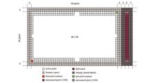
ObjectiveSingle-photon avalanche diodes (SPADs) are in high demand for various applications, particularly in mobile devices, robotics, virtual reality/augmented reality (VR/AR), and autonomous driving. Unlike conventional CMOS image sensors, SPADs operate in a high breakdown voltage (BV) mode to achieve high gain. However, high BV leads to increased power consumption, which is undesirable for mobile applications. A high photon detection efficiency (PDE) is critical for extending the detection range of dTOF systems and minimizing transmitter power consumption. In addition, maintaining stable SPAD performance across different temperatures is essential due to the complex environments in which they are used. We present the design and characterization of a high-performance SPAD array sensor, VA6320, suitable for various applications such as mobile and VR/AR.MethodThe sensor described here is manufactured using a 3D stacking process with Cu—Cu hybrid bonding. The SPAD wafer is fabricated using a 55 nm backside illumination (BSI) process, while the ASIC wafer is fabricated using a 40 nm logic process. BSI CMOS image sensor technology with 3D stacking is applied to SPAD technology to enhance PDE, complemented by optical structures such as anti-reflection coating (ARC) and pyramid surface for diffraction (PSD). In addition, the design of the top tier is customized to achieve high performance, including low breakdown voltage, low temperature coefficient, minimal jitter, reduced crosstalk, and low afterpulsing.Results and DiscussionsIn this study, a 20 μm pitch SPAD is designed. Thanks to a special implant design, a low breakdown voltage of 16.54 V at room temperature and a low temperature coefficient of 18 mV/℃ are achieved (Fig. 5). The introduction of anti-reflection layers, microlenses, backside scattering structures, and bottom reflectors contributes to high quantum efficiency and improved photon detection efficiency, with PDE values of 28.8% at 905 nm and 22.4% at 940 nm. The temperature dependence of the dark count rate (DCR) is characterized (Fig. 7), showing an exponential increase with temperature between -20 and 80 ℃. The DCR doubles every 20 ℃, suggesting that the DCR may be due to trap-assisted tunneling. The dead time is 33 ns at room temperature and decreases with temperature (Fig. 8), likely due to the temperature dependence of the recharge current. The full width at half maximum (FWHM) of SPAD timing jitter is about 350 ps (Fig. 9), with an approximately one-nanosecond diffusion tail, indicating that the epitaxial layer is not fully depleted. The timing jitter remains stable across different temperatures. Figure 10 shows the distribution of avalanche events collected under dark conditions, with excessive avalanche events within 0?500 ns considered as afterpulses. The afterpulsing rate is estimated at 0.35% with a 30 ns dead time. Benefiting from excellent optical and electrical isolation due to deep trench isolation (DTI), the device shows low crosstalk of 0.16% for overbias Vex of 2V (Fig. 11). Crosstalk increases with excess voltage and temperature, which is attributed to the PDE’s temperature dependence. Figure 12 shows a light emission distribution of the avalanche process from a region of pixels with the center pixel activated, indicating breakdown mainly occurs in the central PN junction rather than at the edges. Figure 14 shows a gesture point cloud image captured by the SPAD sensor using a high-frame-rate global shutter method.ConclusionsWe report the design and performance characterization of a new type of BSI SPAD. The sensor is manufactured using a 3D stacking process with Cu—Cu hybrid bonding, where the top tier is fabricated using a 55 nm logic process and the bottom tier is fabricated using a 40 nm logic process. By optimizing the device structure and doping to reduce breakdown voltage and its temperature coefficient, the breakdown voltage is 16.54 V at room temperature, and the temperature coefficient is as low as 18 mV/℃. The integration of anti-reflection layers, microlenses, backside scattering structures, and bottom reflectors achieves high quantum efficiency and improved photon detection efficiency, with a PDE of 28.8% at 905 nm and 22.4% at 940 nm. Deep trench isolation enhances electrical and optical isolation, with pixel crosstalk below 0.5%, demonstrating good performance. The SPAD sensor with a 40×30 pixel array successfully provides high frame rate spatial 2D depth maps using a global shutter method, offering an industrial solution for dTOF ranging, with potential applications in mobile phones, camera focusing, AR/VR, and more.
Dec. 16, 2024Vol. 44 Issue 23 2304001 (2024)
Guohui Chen, Liangping Xia, Chunyan Wang, Suihu Dang, Man Zhang, Shuai Wang, Hong Tu, Jingtian Lan, and Chunlei Du
ObjectiveLaser beam-splitting diffractive elements are highly demanded in fields such as laser radar, optical time-of-flight depth sensing, and three-dimensional structured light sensing due to their miniaturization and high diffraction efficiency. With advancements in lithography nanostructure resolution, it is now feasible to produce diffractive elements with small feature sizes and large diffraction angles. However, as the diffraction angle increases, designs based on scalar diffraction theory no longer satisfy the paraxial approximation, leading to significant errors in the uniformity of far-field diffraction spot energy distribution. This makes it difficult to meet the design requirements for large-angle diffraction elements. Furthermore, the pixel-based structure of two-dimensional laser beam-splitting elements often involves hundreds of thousands of design variables, making it challenging for traditional optimization algorithms to achieve uniform beam-splitting. In this paper, we propose a method that combines vector diffraction theory with the adjoint method to optimize the design of large-angle beam splitters. This approach requires only two electromagnetic simulations per iteration to compute the gradient of the evaluation function relative to all design variables, significantly improving design efficiency. Our research aims to enhance the uniformity of large-angle laser beam-splitting diffractive structures.MethodsIn this paper, we propose a design method based on vector diffraction theory and an adjoint method for optimizing large-angle beam-splitting diffractive elements. First, we calculate the initial phase distribution using a non-paraxial scalar iterative Fourier transform algorithm to achieve the desired diffraction angle. Next, we design the dielectric constant distribution by relating the phase to the depth of the beam-splitting diffractive element, allowing for a continuous dielectric constant distribution within the structural region. Finally, the gradient descent direction is calculated using the finite-difference time-domain (FDTD) method and the adjoint method, and the structural parameters are updated accordingly. Using this approach, we design a 7×3 beam-splitting diffractive structure with a wavelength of 632.8 nm, a period size of 2.8 µm×6 µm, and a full diffraction angle of 78°×12°. The design is fabricated using conventional semiconductor processing techniques on UV-curing resin, involving coating, homogenizing, exposure, development, etching, and imprinting.Results and DiscussionsThe variation curve of the evaluation function F and the dielectric constant distribution of the designed two-dimensional laser beam-splitting diffractive element are shown in Fig. 2. The change in the evaluation function with the number of iterations during the process is shown in Fig. 2(a). The total number of iterations is only 75, and the convergence speed is rapid. In addition, increasing the projection intensity β drives the diffraction structure to gradually become binary discrete during the iteration. Comparing the starting point unit structure in Fig. 2(c) with the unit structure after the iteration in Fig. 2(d), it can be seen that as β value continues to increase, the diffraction structure completely transforms into a binary step diffraction structure, which can be directly used for subsequent processing and preparation. The final beam-splitting uniformity error is 21.3%. The fabrication results of the diffraction beam splitter are shown in Fig. 4. A comparison between the fabricated structure in Fig. 4(c) and the theoretical structure in Fig. 2(f) confirms that the experimental results are consistent with the theoretical design. The scanning electron microscope (SEM) image of the cross-section is shown in Fig. 4(d), demonstrating good verticality of the structure. By measuring the depth at 25 different etching points, the average etching depth is found to be 590 nm, which is close to the theoretical depth of 580 nm. The experimental test results of the beam-splitting effect are shown in Fig. 5. The uniformity error of the experimental test data is 29.14 %, which is consistent with the theoretical result. These results confirm the effectiveness of the proposed vector adjoint optimization method for designing beam-splitting laser diffractive elements.ConclusionsIn this paper, we propose a vector optimization method for the design of large-angle laser diffractive elements. By requiring only two vector calculations to obtain the gradient of the evaluation function for all design variables, this method significantly simplifies the optimization process for large-angle diffractive elements. The number of iterations required for optimization is reduced and diffraction uniformity is improved. Using this method, we design a laser beam-splitting diffractive element with a wavelength of 632.8 nm and a full diffraction angle of 78°×12°. The structure is fabricated using conventional refractive index materials (with a refractive index of 1.53) with a uniformity error of 29.14%. This work provides a valuable technical reference for the fabrication of high-uniformity, large-angle diffractive elements using conventional materials.
Dec. 10, 2024Vol. 44 Issue 23 2305001 (2024)
Yi Yang, Yibo Feng, Yuang Dou, Jianlei Zhang, Fengtao He, Yunzhou Zhu, Xiaobo Wang, Xu Gao, and Leyan Li
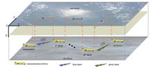
ObjectiveUnderwater high-speed wireless communication technology is rapidly advancing, driven by increased exploration for military and scientific activities in the oceans. Compared to traditional acoustic and radio frequency communications, underwater wireless optical communication offers higher bandwidth, speed, and confidentiality. However, end-to-end wireless optical communication faces limitations in transmission distance underwater and significant environmental constraints on radiation. Given the diverse underwater environment and potential obstructions that can interrupt long-distance communication links, employing an underwater wireless optical relay network communication system can extend communication distances and enable flexible networking. Yet, the underwater wireless optical relay communication system and associated relay forwarding protocol are still in the research and simulation phase, focusing mainly on transmissive transmission. Therefore, our study designs a hierarchical data processing structure and bootstrap sequences based on the ethernet data communication interface. We also design a serial-like character frame structure and a data forwarding protocol to address the challenges of long-distance underwater transmission of standard ethernet data and flexible networking communication.MethodsTo facilitate underwater wireless optical relay networking communication, we design an ethernet data wireless optical relay transmission protocol under a chain network topology, using the RJ45 standard ethernet interface and data transmission protocol. This design is geared towards realizing an underwater wireless optical relay communication system. First, considering the heterogeneous data types and rates between the 100 Gbit ethernet channel and the optical channel, we develop a data matching algorithm. By writing code and utilizing field programmable gate array (FPGA) hardware, we achieve the conversion from high-speed parallel electrical signals to low-speed serial optical signals. Moreover, addressing the issues of high power consumption and data distortion in underwater wireless optical communication systems, we design bootstrap sequences, a serial-like character frame structure, and a line coding algorithm. These innovations ensure reliable data transmission in the underwater relay communication system while significantly reducing system power consumption. Finally, we construct and test a three-node underwater wireless optical relay system, implementing the underwater wireless optical relay forwarding protocol and achieving end-to-end communication among the three nodes.Results and DiscussionsWe establish an experimental environment for a three-node cascade relay system, converting 100 Mbit/s parallel ethernet data to 4 Mbit/s serial optical channel data. Theoretical analysis and experimental results indicate that the maximum ethernet frame length that can be received without loss is 400 B, given a storage capacity of 3300 B, an optical channel rate of 4 Mbit/s, and an ethernet electrical interface frame sending interval of 1 ms. As frame length increases, the probability of correctly receiving decreases rapidly due to limited storage capacity in the FPGA information processing unit. Increasing the time interval between transmitted frames or the optical channel rate improves the probability of correct frame reception. Additionally, the bootstrap sequence length correlates with receiving optical power and the optical channel rate. When the receiving optical power reaches its limit, the number of bytes in the bootstrap sequence increases linearly with the optical channel rate to achieve transmission without frame loss. This relationship exists because background optical noise affects high-speed signals more pronouncedly when the receiving optical power reaches its sensitivity limit, necessitating more bytes of the bootstrap sequence to counteract the background light effect. Further experiments revealed that, under similar conditions for correct frame reception probability, the terminal B node’s received optical power limit is 12.5 nW in a two-node end-to-end system, while the terminal C node’s limit is 17 nW in a three-node cascade relay system. This outcome effectively doubles the communication distance in the cascade relay system compared to the two-node system.ConclusionsOur study introduces an innovative wireless optical data and relay forwarding protocol based on the ethernet RJ45 interface protocol to extend underwater wireless optical communication ranges. Utilizing high-power wireless optical signal transmission, high-sensitivity reception, and an FPGA system, we realize a three-layer structure for data processing, serial-type data processing, and channel codec layers. This structure facilitates the conversion and integration of different data types and rates, enhancing effective relaying and forwarding through parsing and reorganization of optical channel data. Our approach significantly boosts transmission distance without compromising the system performance of underwater wireless optical communication. Furthermore, we propose and implement a bootstrap sequence and a serial port-like character frame structure based on a layered data processing strategy, which reduces device energy consumption and enhances communication reliability.
Dec. 17, 2024Vol. 44 Issue 23 2306001 (2024)
Xinxin Wu, Jianhua Chang, Ziyi Hu, Xinyi Ke, and Yang Min
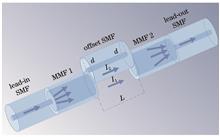
ObjectiveEfficient and accurate monitoring of seawater temperature and salinity is crucial for marine resource exploitation, ecosystem protection, and assessing concrete structure durability. Compared to conventional conductivity-based sensors, optical fiber sensors are rapidly advancing in marine environmental exploration due to their advantages, such as corrosion resistance, compact size, resistance to electromagnetic interference, and ease of long-distance signal transmission. Previous optical fiber thermohaline sensors often have limited sensitivity, complex preparation processes, and assume a linear, non-interfering relationship between interference angle wavelength and temperature/salinity, with data decoupling achieved through matrix equations. This assumption, however, leads to significant calculation deviations. Therefore, developing a high-sensitivity fiber optic sensor for temperature and salinity measurement, along with a high-precision decoupling algorithm, is essential. In this paper, we propose a semi-open cavity Mach?Zehnder interferometer (MZI) sensor, whose sensing path is in direct contact with seawater. Variations in temperature and salinity influence the refractive index of seawater, altering the phase difference between two interfering light beams. By tracking the drift in interference angle wavelength, both temperature and salinity can be measured with high sensitivity. To address the crosstalk between temperature and salinity, a quadratic polynomial surface fitting nonlinear decoupling algorithm is applied, effectively eliminating crosstalk and reducing measurement deviations.MethodsA segment of single-mode fiber (SMF) is placed between two coaxial multi-mode fibers (MMF 1 and MMF 2) through lateral offset splicing. MMF 1 and MMF 2 are spliced with input and output SMF sections, respectively. Light introduced into the SMF expands within MMF 1 before encountering the first offset weld. It then divides into two parts: one path propagates in seawater as the sensing arm, while the other travels through the SMF envelope as a reference arm. MMF 2 then couples the light from seawater and the reference arm back into the outgoing SMF. Variations in seawater temperature and salinity alter the phase difference between the two interference paths, shifting the MZI spectrum. By monitoring this interference angle wavelength, the sensor can measure temperature and salinity with high sensitivity. The simultaneous measurement of temperature and salinity is performed in real-time using the quadratic polynomial surface fitting nonlinear decoupling algorithm. To assess the accuracy of this decoupling approach, results are compared to both the transfer matrix method and a nonlinear decoupling algorithm without interaction terms. This comparison demonstrates the importance of interaction terms and validates the effectiveness of the quadratic polynomial surface fitting-based decoupling approach, which minimizes both maximum and average temperature and salinity errors.Results and DiscussionsUnder a fixed salinity of 30‰, the interference inclination positions (Dip 1 and Dip 2) at temperatures of 18, 20, 22, 25, 27, and 32 ℃ are determined to the MZI’s temperature response characteristics (Fig. 5). As temperature increases, the MZI spectrum’s interference inclination shifts towards longer wavelengths. The relationship between interference inclination position and seawater temperature is best described by a quadratic polynomial, with a maximum temperature sensitivity of 2.1636 nm/℃ for Dip 1 and 1.8997 nm/℃ for Dip 2. For salinity response testing, seawater samples with salinities of 30‰, 33‰, 35‰, 37‰, and 40‰ are prepared and tested at a constant temperature of 18 ℃ (Fig. 6). With increasing salinity, the MZI’s spectrum’s interference inclination moves towards short wavelengths. Linear fitting of the interference inclination wavelength against salinity results in salinity sensitivities of -2.65 nm/‰ for Dip 1 and -2.5948 nm/‰ for Dip 2, respectively. To address temperature?salinity crosstalk, a quadratic polynomial surface fitting decoupling algorithm is used, achieving a maximum temperature deviation of -0.4031 ℃ and a salinity deviation of -0.1242‰, with an average deviation of 0.1599 ℃ and 0.0779‰, respectively.ConclusionsIn this paper, we propose an all-fiber MZI structure based on core offset, proving that a nonlinear decoupling algorithm using quadratic polynomial surface fitting is effective for simultaneous seawater temperature and salinity measurement. The sensor’s semi-open cavity serves as the sensing path, in direct contact with seawater, while the biased SMF envelope acts as the reference path. Changes in seawater properties alter the phase difference between these transmission paths. By recording two selected interference inclination wavelengths in the transmission spectrum, temperature and salinity can be measured with high precision. The experimental and correlation analyses show that the quadratic function more accurately models the relationship between the interference angle wavelength and seawater temperature, while both quadratic and linear functions can describe the relationship with seawater salinity. Due to the cross-interference between temperature and salinity, a quadratic polynomial surface fitting algorithm is applied to demodulate these parameters, effectively eliminating crosstalk and reducing measurement deviation. The sensor demonstrates strong repeatability, good stability, and high precision, providing a valuable reference for detecting seawater environmental parameters.
Dec. 17, 2024Vol. 44 Issue 23 2306002 (2024)
Xixiang Ma, Hongyu Ren, Hui Qiao, Zizhou Wang, Bingqiang Zhang, and Sanzhao Wang
ObjectiveMost mainstream optical fiber arrays on the market are made of glass optical fibers with mature technology, but these products have many limitations such as complicated preparation process, heavy mass, fragility, proneness to corrosion, poor biocompatibility, and high cost. In contrast, characterized by light weight, flexibility, resistance against interference and impact, and excellent biocompatibility, polymer optical fiber arrays have opened up new paths for performance enhancement in optical imaging technologies. We study the unique properties of polymer optical fiber arrays, especially in terms of highly flexible and biocompatible applications, and optimize key processes during the new preparation method. Meanwhile, an in-depth optimization study of the hot pressing process is carried out by adopting a design model based on the Box-Behnken response surface method. By systematically examining the effects of key parameters on the optical transmission, such as hot pressing temperature, pressure, and hot pressing time, we intuitively understand the interactions among the factors by building a mathematical model between the parameters and the response, and provide an efficient method to explore the hot pressing molding conditions. This optimization process not only enhances the preparation technology of polymer optical fiber array panels but also lays a solid foundation for their wide application in optical imaging. By conducting systematic evaluation, we expect to reveal the potential of polymer optical fiber arrays in optical imaging, which will promote the further development and wide application of related technologies. This will not only revolutionize the optical imaging technology but also inject new vitality into the development of related industries.MethodsWe employ fluorinated polymethyl methacrylate as the fiber material, which is finally hot pressing molded by a series of precise preparation processes, including key steps such as fiber preform forming, fiber drawing, fiber bundling, and arranging. To further enhance the reliability and optical imaging quality of hot pressing molding, we adopt the Box-Behnken design methodology to systematically explore the complex relationship between the hot pressing process factors (hot pressing temperature, pressure, and hot pressing time) and key response values of transmission. By utilizing the Box-Behnken design (BBD), a multifactor and multilevel experimental model is built, which can comprehensively consider the interactions among the process factors, and thus predict and optimize the process parameters more accurately. Subsequently, the fitting effect of the response model and its significance are rigorously and statistically verified by variance analysis to ensure the reliability and validity of the model. On this basis, the model response values are optimized in our study, and the optimal combination of hot-pressing process parameters is finally determined via iterative calculations and experimental validation, thus ensuring high transmission and excellent imaging quality of the polymer optical fiber array panels. Based on the prepared polymer optical fiber array panels, key performance indicators such as transmission, image displacement, magnification, and spatial resolution are systematically evaluated. These experiments not only verify the practical effectiveness of polymer optical fiber array panels in optical imaging but also provide valuable data support for further optimization and improvement of the preparation process.Results and DiscussionsPolymer optical fiber array panels with high transmission and excellent imaging quality are successfully prepared by employing the fiber preform forming-drawing-bundling-hot pressing process. This achievement is attributed to the precise superposition and optimization of key steps in the fabrication process, which both improves the surface quality of the drawn optical fibers and substantially improves the optical fiber coupling quality and overall mechanical strength and stability. As shown in Fig. 10, the internal structure of the prepared polymer fiber array unit is tight and seamless, with high array consistency and no obvious defects. BBD fits the hot pressing process parameters well, and the reliability of the hot pressing process model is also further verified by the methodology to analyze the results in Table 3 and the characteristics of the residual plots in Fig. 8. According to the response surface method, the optimal process conditions are optimized as follows: hot pressing temperature 181.8 ℃, pressure 0.28 MPa, and hot pressing time 40.8 min. The transmission of the 5 mm polymer optical fiber array panels prepared by this method reaches 94.07%. By referring to Fig. 12 for transmission comparison, the transmission of our prepared polymer optical fiber array panel is much higher than those produced by INCOM and the 3D printing method respectively. As can be seen in Fig. 15(b), the words on the text float on the surface of the output end of the polymer optical fiber panel without any aberration, and the transmission effect remains sound as the thickness of the panel increases. These experiments not only verify the practical effectiveness of polymer optical fiber array panels in optical imaging but also provide valuable data support for further optimization and improvement of the preparation process.ConclusionsBy adopting the ANOVA of the BBD model, it is found that in the linear term, the hot-pressing temperature (x1) has the most significant effect on the transmission, while in the quadratic term, the interaction between pressure and hot-pressing time (x2x3) exerts the most significant effect on the transmission. In the optimal conditions (hot pressing temperature of 181.8 ℃, pressure of 0.28 MPa, and hot pressing time of 40.8 min) obtained by the response surface method, polymer optical fiber array panels with transmission as high as 94.07% are successfully prepared in our study, and this result is significantly better than those of the state-of-the-art methods. The excellent performance of the polymer optical fiber panel in terms of image transmission accuracy is verified by the accurate measurement of image displacement and magnification measurement and resolution test as well as the panel imaging guidance capability. The experimental results show a maximum image displacement of 240 μm, a magnification of (100±2)%, and a resolution of 10.10 lp/mm, demonstrating the superior performance of the polymer optical fiber array panel in terms of image transmission accuracy. Compared with the polymer optical fiber panel prepared by Wang et al. via 3D printing and the commercial polymer optical fiber panel of INCOM, the transmission in our study reaches 94.07% at a thickness of 5 mm. This significant improvement not only proves the effectiveness of the new process but also provides new possibilities for the application of polymer optical fiber arrays in optical imaging and optical communication, thereby laying a solid foundation for expanding applications in related fields.
Dec. 10, 2024Vol. 44 Issue 23 2306003 (2024)
Yang Min, Jianhua Chang, Xinyi Ke, and Xinxin Wu
ObjectiveIn recent years, with the improvement of sensor accuracy and performance requirements in biomedicine, chemical sensing, and environmental monitoring, the demand for multi-parameter simultaneous monitoring is growing. For example, in marine environmental monitoring, it is necessary to detect the refractive index, pH, and temperature simultaneously. However, most current sensors have complex structures, poor mechanical strength, and small dynamic measurement ranges, making it difficult to meet the simultaneous measurement needs in complex environments. Therefore, it is essential to develop a kind of optical fiber sensor with simple structures, high performance, and large measurement ranges, which can realize multi-parameter simultaneous detection in complex environments. We propose an optical fiber sensor based on surface plasmon resonance (SPR) and Mach?Zehnder interference (MZI) effects combined with empirical mode decomposition (EMD) to simultaneously detect the refractive index, pH, and temperature.MethodsWe combine the SPR and MZI effects in the multimode optical fiber-hollow core optical fiber-multimode optical fiber (MMF-HCF-MMF) structure with EMD to achieve simultaneous detection of the refractive index, pH, and temperature. First, the principles of the two effects are analyzed, the performance parameter formulas of SPR and MZI are derived, and simulation is adopted to verify the feasibility of the theory. Meanwhile, we analyze the principles and steps of EMD and its effectiveness in enhancing the free spectral range (FSR) of the interference spectrum. Then, an optical fiber sensor based on the MMF-HCF-MMF structure is fabricated, and the side of HCF is divided into region I and region II by silver nanofilm and polyacrylic acid/chitosan (PAA/CS), which are employed to measure the refractive index and pH respectively. Additionally, the MZI interference spectrum generated by the ambient temperature change in the region-Ш is decomposed into intrinsic mode functions (IMFs) via EMD to achieve temperature measurement. Finally, a refractive index, pH, and temperature experimental test platform is built to conduct performance testing on the system.Results and DiscussionsThe Refractive index response of the sensor without a pH-sensitive film is first tested, and the corresponding refractive index sensitivity is 2680.26 nm/RIU (Fig. 6). Secondly, the refractive index and pH sensing performances of the sensor are tested. The sensitivity of region I to the refractive index is 2381.71 nm/RIU [Fig. 9(b)], and that of region II to pH is -14.62 nm/pH [Fig. 10(b)]. Then, the effect of temperature on refractive index and pH detection is tested. The sensitivity to temperature in region I and region II is obtained to be -0.14 nm/℃ and -0.17 nm/℃ respectively [Fig. 11(b)]. To reduce the influence of temperature changes, we introduce EMD to obtain the sensitivity of region III to temperature as 85.27 pm/℃ [Fig. 13(f)]. Subsequently, the temperature compensation is realized by the sensing matrix, and the error analysis is performed via adopting the sensing matrix. The results show that the refractive index, pH, and temperature change errors are 2.5%, 2.1%, and 1.8% respectively. Finally, the stability and repeatability of the sensor are verified. The experimental results indicate that the maximum sensitivity errors of refractive index, pH, and temperature are 68.34 nm/RIU, 0.23 nm/pH, and 0.59 pm/℃, respectively. The sensor proposed in our study has better performance and lower cost than other sensors.ConclusionsWe propose and fabricate an optical fiber sensor based on SPR and MZI effects combined with EMD to detect the refractive index, pH and temperature simultaneously. The sensor adopts the structure of MMF-HCF-MMF, and divides the HCF into two independent sensing regions by silver nanofilm and polyacrylic acid/chitosan (PAA/CS) composites, which measure the refractive index and pH respectively. Meanwhile, the interference spectrum generated by MZI is decomposed into IMFs by EMD, and FSR is extended to realize temperature compensation. The experimental results show that the sensor has sensitivity of 2381.71 nm/RIU for the refractive index, -14.62 nm/pH for pH, and 85.27 pm/℃ for temperature. The proposed sensor not only shows high sensitivity and a simple fabrication process, but also has low cost and the ability to detect multiple parameters simultaneously. These characteristics make the sensor have great application potential in marine monitoring, biochemical analysis, and other fields.
Dec. 16, 2024Vol. 44 Issue 23 2306004 (2024)
Shuai Chang, Hang Chen, Peng Zhang, Shuang He, Yuanxin Wang, Hao Yu, Jin Xu, Hang Nan, and Shoufeng Tong
ObjectiveWe aim to investigate the transmission and communication characteristics of the Hypergeometric-Gaussian (HyGG) beam, which exhibits pseudo-nondiffraction, self-focusing, and self-reconstruction characteristics. These properties are expected to enhance the channel capacity of underwater optical communication (UWOC) systems based on orbital angular momentum (OAM). While there is growing interest in the transmission of the HyGG beam through turbulent media, recent research on its performance in underwater channels remains limited. The team led by Shengmei Zhao explores the spiral phase spectrum evolution of the HyGG beam based on the Nikishov oceanic turbulence power spectrum. However, the Nikishov spectrum exhibits a singularity at zero spatial wave number, and the absorption effects of seawater and anisotropic impacts on the transmission of HyGG beam OAM modes have not been adequately addressed. Furthermore, the existing study investigates the OAM detection probability evolution of the HyGG beam only within less than 0.1 times the Rayleigh distance, failing to fully demonstrate its transmission advantages. Thus, it is essential to introduce a new oceanic turbulence power spectrum and conduct theoretical research on the long-distance transmission and communication performance of the HyGG beam in an absorbent and anisotropic oceanic turbulence channel. This research provides a vital reference for designing and improving practical underwater wireless optical communication systems.MethodsTo further investigate the transmission and communication characteristics of the HyGG beam in underwater channels, we introduce a newly proposed oceanic turbulence power spectrum. We comprehensively consider the effects of seawater absorption and anisotropy. Based on the Rytov turbulence approximation theory and the new oceanic turbulence power spectrum, we derive the analytical expression of the OAM spiral phase spectrum for the HyGG beam under absorptive and anisotropic oceanic turbulence. Subsequently, using the established average channel capacity model, we analyze in detail the influence of the HyGG beam parameters, seawater channel parameters, and communication system parameters on the average channel capacity during long-distance transmission.Results and DiscussionsThe influence of oceanic turbulence leads to an increase in spiral wavefront distortion with increasing transmission distance. The vortex beam with OAM mode number gradually disperses its energy into neighboring OAM modes. After transmitting 200 m, the OAM detection probability of the HyGG beam is approximately 20% higher than that of the Gaussian vortex (GV) beam and 10% higher than that of the Laguerre-Gaussian (LG) beam. This is due to the stronger self-focusing ability of the HyGG beam, which results in smaller beam broadening in oceanic channels and fewer turbulent cells with varying refractive indices. Consequently, the HyGG beam exhibits reduced wavefront distortion and higher purity of OAM signal modes during transmission in oceanic channels (Fig. 3). For practical applications, selecting the appropriate p value of the HyGG beam according to different communication distances effectively enhances system performance (Fig. 4). The average channel capacity of the HyGG beam decreases with increasing l0, favoring larger p values for higher average channel capacity due to faster divergence of the HyGG beam with larger l0 values (Fig. 5). To mitigate the effects of seawater absorption in long-distance UWOC, we recommend the HyGG beam in the 410?490 nm range. Additionally, selecting the appropriate initial waist radius of the HyGG beam according to actual underwater communication distance requirements maximizes average channel capacity (Fig. 6). The average channel capacity of the HyGG beam increases with increasing turbulence scale and decreases with increasing outer scale. Furthermore, the channel capacity increases with the anisotropy parameter, benefiting transmission and communication in seawater (Fig. 7). The average channel capacity decreases with increasing root mean square temperature dissipation rate χT and temperature-salinity gradient ratio w, and increases with the kinetic energy dissipation rate ε. Higher values of w, χT, or lower values of ε, increase oceanic turbulence intensity, exacerbating wavefront distortion and deteriorating transmission and communication performance of the HyGG beam in oceanic channels (Fig. 8). At 50 m, the average channel capacity of the HyGG beam is nearly independent of the size of the receiving aperture. With increasing transmission distance, the average channel capacity initially increases and then decreases with larger receiving aperture size, stabilizing at Ra=3 mm with a peak value. These phenomena can be explained as follows: 1) at shorter transmission distances, optical signal energy attenuation and inter-mode crosstalk are minimal, and the received optical power significantly exceeds system noise power N0, thus channel capacity is primarily determined by OAM signal mode power and crosstalk power, with little influence from varying the receiving aperture size; 2) Although reducing the receiving aperture size can enhance OAM detection probability, longer distances and smaller receiving apertures also result in greater power loss. When received optical power approaches N0, average channel capacity is primarily influenced by received optical power (Fig. 10).ConclusionsWe derive analytical expressions for the OAM detection probability and average channel capacity of the HyGG beam in absorptive anisotropic oceanic channels based on the Rytov approximation and generalized Huygens-Fresnel principle. Our analysis covers the intensity distribution of the HyGG beam in turbulence-free channels and extensively studies the influence of source parameters, channel environmental parameters, and communication system parameters on the transmission and communication quality of the HyGG beam. The results indicate that the self-focusing ability of the HyGG beam increases with the hollowness parameter. The influence of oceanic turbulence on the HyGG beam increases with transmission distance, temperature variance dissipation rate, turbulence inner scale, and OAM mode number, while it decreases with kinetic energy dissipation rate, turbulence outer scale, and anisotropy parameter. The system’s average channel capacity increases with higher transmit power and OAM channel number. The trend of the communication system error rate is opposite that of average channel capacity. For different communication link lengths, optimal values for HyGG beam wavelength, waist radius, hollowness parameter, and receiving aperture values exist to maximize the system’s average channel capacity. Additionally, due to its self-focusing characteristics, the HyGG beam with hollowness parameter p>0 demonstrates superior transmission and communication performance over LG and GV beams in long-distance transmission. Therefore, The HyGG beam exhibits strong resistance to turbulence and attenuation.
Dec. 10, 2024Vol. 44 Issue 23 2306005 (2024)
Xuan Wu, Bin Yang, Xianfeng Li, Junqiang Zhang, and Tianjiao Lu
ObjectiveSpatial-spectral coupling multispectral imaging is an innovative technology that integrates spatial and spectral information using color filter array sensors and multi-bandpass narrowband filters. This approach allows each pixel to capture data from multiple spectral bands. Due to the inherent coupling of spatial and spectral data, traditional radiometric calibration methods are insufficient for accurately determining radiometric response coefficients. Research on the calibration of such multispectral cameras remains limited. Current methods often focus solely on spectral response, using theoretical energy contribution ratios for each band as decomposition coefficients. However, these methods lack a well-defined radiometric response model and have not undergone sufficient experimental validation, leading to inaccuracies. Therefore, further research is needed to develop precise calibration methods and to solve for accurate radiometric response coefficients in this multi-band spatial-spectral coupled imaging system. Improving the radiometric accuracy of these systems will ensure reliable data for a wide range of applications.MethodsIn this study, we use a four-channel multispectral camera to construct a radiometric response model based on radiative transfer theory, describing the complete spectral radiative transfer process. A laboratory radiometric calibration method using a combination of multiple light sources is proposed, enabling variation in both the spectral and radiometric dimensions. This approach generates an overdetermined system of equations for the radiometric response coefficients. By calculating the energy contribution ratios for each band from the spectral response and converting these ratios into initial estimates of the radiometric response coefficients, the method avoids incorrect local optima when solving the overdetermined equations. The gradient descent method is then applied to compute the optimal radiometric response coefficients, ensuring practical physical relevance. This approach, which integrates theoretical calculations with experimental calibration data, significantly enhances the reliability of the derived radiometric response coefficients.Results and DiscussionsUsing the proposed calibration method, we determine optimal radiometric response coefficients for the four spectral bands (Table 3). These coefficients are then used in both laboratory and field accuracy verification, with the results as follows. 1) Laboratory accuracy verification: data not involved in deriving the optimal radiometric response coefficients are used. The mean relative error of the retrieved radiance for all bands is found to be less than 5% (Fig. 8). 2) Field calibration: a relationship between the reflectance of a diffuse reflection panel and the exit radiance is established. Radiance data are collected using the multispectral camera, while reflectance data are measured with an ASD device. Field calibration coefficients are calculated (Table 4), and reflectance validation shows that the error distribution across all bands is uniform, with a mean relative error within 6% (Table 6, Fig. 11). 3) Uncertainty analysis: the uncertainty in the radiometric calibration transfer chain is analyzed, revealing that the absolute calibration uncertainty for each band is less than 5% (Table 7).ConclusionsIn this study, we propose a comprehensive radiometric response model for spatial-spectral coupling multispectral camera, based on radiative transfer theory. We introduce a laboratory calibration method using multiple light sources, allowing for variation in both spectral and radiometric dimensions. The initial radiometric response coefficients are derived from theoretical spectral response calculations, and the gradient descent method is used to determine the optimal coefficients. We validate the calibration accuracy through both laboratory and field experiments. Our model and method significantly enhance the radiometric accuracy of spatial-spectral coupling multispectral imaging systems, eliminating uncertainties caused by overlapping radiometric responses between different spectral bands. These findings hold significant theoretical and practical values for advancing research and applications of this technology.
Dec. 10, 2024Vol. 44 Issue 23 2311002 (2024)
Zixuan Yang, Xuesong Jiang, Yuchen Tang, and Jingjing Wu
ObjectiveThe single-pixel imaging (SPI) system requires only a single-pixel detector to measure the total light intensity and is not sensitive to phase, which makes it suitable for imaging objects in complex environments. If an object is obstructed by an opaque obstacle, and the obstacle is sparsely distributed, the obstacle’s signal and the object’s signal can be separated over time using the principle of light time of flight, which allows for image reconstruction of the object. For large-area occlusions, the current effective method combines the self-reconstruction characteristics of Bessel beams to achieve the SPI of the object. However, existing studies have only demonstrated the feasibility of this approach without deeply analyzing the underlying factors such as the shape and position of obstacles and the conditions for complete imaging. We tackle this issue by exploring the influence of different types of obstacles on Bessel SPI, as well as the conditions for effective imaging, thus providing a reference for applying Bessel beams in SPI.MethodsThe Bessel beam is generated by projecting an annular slit onto the DMD and combining it with a Fourier lens. By shifting the annular slit in a specific sequence, we can scan the Bessel beam across the object’s surface accordingly. Bessel-SPI leverages this scanning Bessel beam as the illumination mode in SPI, combined with a compressed sensing algorithm. In this study, we analyze how the shape and position of obstacles affect the Bessel beam, the beam’s self-reconstruction after occlusion, and the resulting SPI imaging. We also define the conditions needed for complete imaging based on the Bessel beam’s non-diffraction and self-reconstruction distances. When these conditions are met, Bessel-SPI can produce a full image of the object. Comparing the transmission and SPI imaging results of the Bessel beam and Hadamard mode under identical occlusion conditions highlights the advantages of Bessel-SPI for imaging occluded objects.Results and DiscussionsFirst, the field of view changes of the object in different positions are compared in the absence of obstruction, as shown in Fig. 4, along with the image quality under different sampling times. This demonstrates that Bessel-SPI can achieve image quality comparable to Hadamard-SPI at the same sampling rate, as shown in Fig. 5, thus verifying the feasibility of Bessel-SPI. Secondly, obstacles are classified into central occlusion type and peripheral occlusion type. For central occlusion type obstacles, simulations are conducted for the Bessel intensity distribution on the object surface and the corresponding Bessel-SPI results. It is proved that when the distance between the object and the obstacle satisfies z2>fa/d (where f represents focal length of lens,a represents size of obstacle in x direction,and d represents ring diameter), and the distance between the lens and the object satisfies z1+z2<2Rf/d (where R is the radius of the lens), the central spot of the Bessel beam can self-reconstruct after passing through the obstacle. Thus, Bessel-SPI can image the object completely. For peripheral occlusion type obstacles, the non-diffraction distance of the Bessel beam will be shortened. The object can be fully imaged only when the distance between the object and the lens is less than or equal to z1+z2<z1+fa/d, where a represents the size of the central transmissive region of the obstacle in the x direction. Finally, comparison of the imaging results from Bessel-SPI and Hadamard-SPI under the same occlusion conditions shows that the experimental results align with the theoretical and simulation results.ConclusionsBased on the self-healing characteristics of Bessel beams, a scheme is proposed using scanning Bessel light as the illumination mode for SPI experiments. The self-healing characteristics of Bessel beams and the imaging results of Bessel-SPI are analyzed under different shapes and positions of obstacles. The simulation results show that Bessel-SPI can achieve image quality similar to Hadamard-SPI when there are no obstacles. In the presence of obstructions, the commonly used Hadamard-SPI lacks obstruction resistance. However, when combined with the compressed sensing algorithm, Bessel-SPI can perform SPI for obstructed objects at a low sampling rate and exhibits greater obstruction resistance. The simulation results also demonstrate that for central occlusion type obstacles, when z2>Zmin and z1+z2<Zmax, Bessel-SPI can capture the complete structure of the object, where Zmin=fa/d. For peripheral occlusion type obstacles, the non-diffraction distance of the Bessel beam becomes Zmax'=z1+fa/d. Bessel-SPI can only obtain the complete structure of the object when the object’s position satisfies z<Zmax'. In this paper, we analyze the applicability of SPI for the special case of opaque obstacle occlusion and improve the imaging research of SPI under such conditions. This work can be extended to dynamic and 3D objects, enabling SPI for occluded moving objects and occluded 3D objects. In addition, leveraging the inherent characteristics of SPI, Bessel-SPI can maintain imaging capabilities in more complex environments, such as line-of-sight imaging under partial occlusion.
Dec. 16, 2024Vol. 44 Issue 23 2311003 (2024)
Zhen Zhang, Xuefeng Zeng, Yang Liu, Lingjie Wang, and Xuejun Zhang
ObjectiveThe angular resolution of an optical system is inversely proportional to the aperture size of the telescope. However, increasing the telescope’s aperture places higher demands on precision manufacturing, and large aperture systems often require complex mechanical structures. This leads to high production costs, longer manufacturing cycles, and stricter rocket launch requirements during orbital deployment. Therefore, achieving lightweight and low power consumption while maintaining high resolution is a critical challenge for optical systems. To address this, researchers at Lockheed Martin and the University of California, Davis, have proposed integrated interferometric imaging technology. By combining the microlens arrays with photonic integration chips, they process optical signals from matched lenses to capture complex coherence across multiple spatial frequencies, corresponding to the far-field target. Using the van Cittert-Zernike theorem, the light intensity distribution of the observed target is reconstructed through inverse Fourier transformation. Current research on integrated interferometric systems mainly focuses on three areas: microlens array structures, photonic integrated chip designs, and image recovery algorithms. These studies have primarily focused on the simulation process of the photonic integrated interference system. However, they only consider the coupling efficiency from the microlens array to the optical waveguide as the limiting factor of the field of view, without adequately investigating the influence of spatial aliasing caused by the discrete spectral distribution. To address this gap, we examine the effect of the minimum baseline length on imaging in integrated interferometric systems, which is crucial for advancing their practical application.MethodsThe study involves both theoretical analysis and computer simulation. First, we construct a frequency domain filter and perform an inverse Fourier transform to obtain the spatial convolution kernel of the integrated interferometric system. We then analyze this convolution kernel to determine the maximum object field width that prevents spectral aliasing. A computer simulation process is designed to verify these theoretical conclusions. This simulation includes the following steps. First, the observation image is input, followed by the construction of the microlens array based on the existing cobweb layout. Next, the coupling efficiency for each object field, corresponding to different microlenses at various positions, is calculated using the coupling efficiency formula. Then, interferometric baselines of different lengths are constructed through head-to-tail matching, and the complex coherence is achieved using the four-step phase-shifting algorithm. The image is then reconstructed using the inverse Fourier transform, which is used to calculate the image width. Finally, the quality of the recovered image is evaluated using root mean square error (RMSE) and peak signal-to-noise ratio (PSNR).Results and DiscussionsBased on the sampling theorem, we analyze the field of view of the integrated interferometric system, highlighting the spatial aliasing effect caused by head-to-tail matching of microlens arrays. The relationship between the minimum baseline length and the field of view is then derived. Based on the principles of the integrated interferometric system, a simulation process is developed to enable imaging of the observation target by adjusting the minimum baseline length. The simulation results demonstrate that when the minimum baseline length exceeds the field of view limit, the system’s imaging quality significantly degrades due to spatial aliasing. This confirms the constraint between the minimum baseline length and the field of view size.ConclusionsThe analysis demonstrates that increasing the minimum baseline length improves the system’s resolution. However, surpassing the maximum field of view limit leads to rapid degradation in imaging quality due to spatial aliasing. Therefore, while increasing baseline length improves resolution, the limiting effect on the field of view must be carefully considered. By adjusting microlens spacing, two operating modes are proposed: short-baseline for a large field of view and long-baseline for a small field of view. This strategy aims to optimize the performance of integrated interferometric systems across various application scenarios.
Dec. 16, 2024Vol. 44 Issue 23 2311004 (2024)
Kailiang Xue, Youxing Chen, Zhaoba Wang, and Wenna Zhang
ObjectiveWhen detecting defects in multi-layer adhesive structures using a terahertz frequency modulated continuous wave (FMCW) detection system, the unidirectional nature of reflection-based scanning can lead to overlapping information blind spots, which affects tomographic imaging quality. Specifically, defects at the same horizontal location but at different depths may overlap or be occluded.MethodsTo assess the effectiveness of the proposed methods, scenarios for both unobstructed and obstructed defect detection were designed for analysis. For unobstructed defects, the target structure (sample 1) is a thermal protection system composed of ceramic matrix composites, insulation felt, and metal plates, bonded sequentially with epoxy resin. Adhesive defects of various shapes and sizes are introduced into adhesive layer 1 and adhesive layer 2. For obstructed defects, polyimide foam insulation serves as the primary structure, and it is layered with low-reflective (PVC) and high-reflective (coins, key) impurities, referred to as sample 2 and sample 3, respectively. For tomographic imaging, an image restoration algorithm is proposed. Initially, mask blocks are labeled on the near-field detection results, and based on this information, target removal is performed on the far-field detection results. The regions are then filled by eliminating differences in texture between the patch elements and the background, yielding detection results containing only the far-field layer’s information. For 3D reconstruction, we discuss the effects observed in all three detection scenarios. Specifically, in scenarios similar to sample 3, a multi-view scanning method is introduced to minimize blind spots and achieve more complete 3D reconstructions.Results and DiscussionsThe original detection results confirm that overlapping information and defect occlusion are common in cases involving thin or high-reflectivity defects (Figs. 5 and 7). For low-reflectivity defects, high-quality tomography imaging is achieved by selecting characteristic features from different depth layers (Fig. 6). By applying the proposed image restoration algorithm, we directly output F1 as I1 and use defect information from F1 to mask and restore textures in F2, producing an imaging result that contains only the current layer’s defect information (Figs. 10 and 11). However, for high-reflectivity defects, some useful information is still lost during tomography imaging and 3D reconstruction. To address this, a multi-view scanning approach is proposed. Results from two scans are registered to generate a complete 3D reconstruction (Fig. 13).ConclusionsThe unidirectional nature of reflective terahertz detection significantly affects detection due to information overlap and blind spots. We propose using image restoration and multi-view scanning to mitigate these issues. These methods are validated on two-layer adhesive structures, providing new insights into the application of terahertz nondestructive testing technology in engineering. Future studies should explore multi-layer structures, especially those involving high-reflectance occlusion defects, from various perspectives, including front, top, and side views.
Dec. 16, 2024Vol. 44 Issue 23 2311005 (2024)
Zechun Lin, Huiping Liang, Lihao Liu, Baoqiong Wang, Yi Zhang, Yueqiang Zhang, Xiaolin Liu, and Qifeng Yu
ObjectiveOutdoor large structures, such as long-span bridges and high-rise buildings, experience deformation due to various complex loads during use. Structural monitoring plays an important role in ensuring the safety and extending the service life of these structures. Photogrammetry is increasingly used in structure monitoring due to its high precision, non-contact, and dynamic measurement capabilities. However, outdoor camera systems are susceptible to environmental influences. Temperature fluctuations can induce internal thermal effects within the camera, leading to image point drift. This drift becomes more pronounced with long-term temperature variations spanning years and seasons. Experiments have shown that a camera temperature fluctuation of 50 °C can cause an image point drift of approximately 7 pixel. Furthermore, due to the optical lever principle, this error is significantly amplified with increasing observation distances, limiting the application of high-precision visual measurement. In this study, we derive a camera image point drift model based on temperature-induced image plane motion. This model establishes a mathematical relationship between image point drift and changes in key camera parameters. Subsequently, we use regression analysis to obtain the camera's temperature drift effect model and implement compensation for temperature-induced image point drift. We aim to provide strong support for applying photogrammetry technology in long-term structural monitoring.MethodsWe derive the camera image point drift model from the image plane using the line of sight principle of camera imaging. This model clarifies the mathematical relationship between the image point drift and the changes in key camera parameters. To analyze the effects of wide temperature ranges and varying temperature rates on image drift, we utilize a temperature control chamber environment and systematically collect experimental data. This approach enriches the model's verification basis and improves image drift prediction accuracy. We use regression analysis to build a mapping model between temperature and variations in camera parameters, predicting and compensating for temperature-induced image point drift in both indoor and outdoor environments.Results and DiscussionsStarting from the camera image plane, we decompose internal temperature-induced changes into translations and rotations of the image plane. This approach eliminates the need to calculate camera pose during the solution process, avoiding errors from pose estimation and simplifying computations. Compared to image point drift models derived directly from the pinhole imaging model, our proposed model exhibits a reduction of approximately 2% in solution error (Table 3), demonstrating the feasibility. In indoor temperature variation experiments, multiple sets of temperature variation tests with different temperature ranges and rates are conducted to observe the temperature drift phenomenon in cameras. We find that the change in principal point coordinate and temperature are not simple linear relationship, whereas the relationship between temperature and focal length variation exhibits a strong linear trend, consistent with the understanding that the thermal expansion coefficient of solids is constant. By utilizing the camera temperature effect model to correct the image point drift phenomenon, we reduce the average error of image point drift by 89.34% (using Gaussian process regression as an example) (Fig. 8), effectively demonstrating the model's compensation effectiveness. However, a comprehensive and detailed analysis of the specific trends and mechanisms of camera parameter changes under different temperature ranges and temperature variation rates has yet to be undertaken for the designed multi-group temperature-controlled experiments. To test the compensation effect of the model in real-world environments, we conduct outdoor experiments. Over a nearly 24-hour monitoring period, the average displacement errors in the two experimental groups are reduced by 79.31% and 85.71% respectively (Fig. 11), demonstrating the strong effectiveness of the proposed camera temperature effect model even in outdoor settings. The displacement errors in the outdoor experiments are effectively controlled below the sub-millimeter level, proving that the method can meet high-precision measurement requirements for long-term structural monitoring, providing robust support for structural safety assessment and maintenance decision-making. Nevertheless, the experimental environment does not fully simulate complex natural variations, and the assessment of the model's stability and reliability over long-term monitoring remains insufficient. Future research should focus on real engineering structures, extend the monitoring duration, comprehensively evaluate model performance, and optimize the model to enhance its applicability and accuracy in complex environments.ConclusionsWe propose an image point drift model for cameras, derived from the camera’s image plane, establishing a relationship between image point coordinate variation and camera parameter changes. Subsequently, we validate the model's effectiveness through multiple indoor temperature-controlled and outdoor experiments. In addition, a complete camera temperature drift effect model is constructed by fitting the relationship between camera parameter variations and temperature using regression algorithms. Compensation results show a reduction of 89.34% in image point drift in indoor environments and average displacement errors are reduced by 79.31% and 85.71% in outdoor environments. This demonstrates the model's effectiveness in compensating for temperature-induced image point drift, providing a solid foundation for temperature effect correction in long-term monitoring.
Dec. 17, 2024Vol. 44 Issue 23 2312002 (2024)
Kejun Si, Jing Bai, Jin Wang, Tengfei Meng, Yaodong Li, Li Wang, and Rui Lou
ObjectiveBased on the concept of surface plasmon polaritons (SPPs), we confine the SPPs to metal or insulator interfaces through a metal-insulator-metal (MIM) waveguide. This approach breaks the classical diffraction limit and allows light to be manipulated at the nanoscale. The study of sensing characteristics by modifying the resonant cavity coupled to the straight waveguide has become a research hotspot. However, achieving optimal solutions for the transmission spectrum, sensitivity, number of peaks, and figure of merit (FOM) of the MIM waveguide coupled resonant cavities remains challenging. To meet the requirements of high sensitivity, high FOM, and multiple Fano resonance peaks for waveguide structures and optical refractive index sensors, the transmission characteristics of SPPs are deeply explored, and an innovative structural design is proposed based on this. This design features a single baffle MIM waveguide coupled with two different types of resonant cavities: an octagonal cavity above and a notched ring cavity below. The clever combination of this structure enables interference effects under near-field coupling, eliminates narrow discrete states formed by the metal baffle and wide continuous states formed by the octagonal and notched ring cavities, and results in three different modes of Fano resonance. This model not only effectively improves the sensor’s sensitivity but also significantly enhances the FOM through reasonable structural design. Different coupling paths and coupling strengths excite the three modes of Fano resonance, each exhibiting unique spectral characteristics.MethodsThe proposed MIM waveguide consists of a straight waveguide with a metal baffle, an upper octagonal resonant cavity, and a lower notched ring cavity. The coupling distance between the resonant cavities and the straight waveguide with the metal baffle g=10 nm. The width of the metal baffle in the straight waveguide d=20 nm. The widths of the octagonal resonant cavity, the notched ring resonant cavity, and the straight waveguide w=50 nm. The side length of the octagonal resonant cavity is defined as S, the radius of the notched ring resonant cavity as R, and the notch size of the notched ring cavity as θ. Based on the coupled mode theory, we analyze the generation mechanism of these three Fano resonances in detail. To verify the accuracy of our theoretical analysis, we conduct numerical simulations of the structure using the finite element method, which effectively handles complex geometric structures and boundary conditions. During the simulation, we perform detailed scanning and in-depth analysis of various key parameters, focusing on their impact on refractive index sensing characteristics and FOM. We perform detailed scanning and in-depth analysis of various key parameters, focusing on their impact on refractive index sensing characteristics and FOM.Results and DiscussionsThe three Fano resonance peaks generated by this model are defined as FR 1, FR 2, and FR 3. Our results show that varying the radius of the ring cavity and the angle of the notched ring cavity directly affects the shifts of FR 1 and FR 3 at the peak wavelengths of the transmission spectrum [Figs. 4(a) and 5(a)]. These parameters also impact the FOM of FR 1 [Figs. 4(a) and 5(b)]. Changing the side length of the octagonal cavity affects the shift of FR 2 at the peak wavelength and the fluctuation of its FOM (Fig. 6). We conclude that the resonance peaks of FR 1 and FR 3 can be controlled by adjusting the radius and angle of the notched ring cavity, while FR 2 can be controlled by adjusting the side length of the octagonal cavity. This allows for flexible wavelength selection and adjustment to cope with varying external environments (e.g., air or liquids with different refractive indices). We provide the optimal FOM values corresponding to the structural parameters and determine the adjustment range. By optimizing the system’s structural parameters, we demonstrate the relationship between the refractive index change and wavelength and transmittance [Fig. 7(a)]. As the refractive index changes, the positions at the wavelengths the positions of FR 1, FR 2, and FR 3 shift. The peak transmittance of FR 1 is highly sensitive to the refractive index, while the peak transmissivity of FR 2 increases, and that of FR 3 decreases with increasing refractive index. The position changes of the peak wavelengths of FR 2 and FR 3 are also significant. Fig. 7(b) shows a linear relationship between the refractive index change and the resonance wavelength position. With further optimization of structural parameters and material selection, this model is expected to play a significant role in future practical applications, such as biosensing, chemical analysis, and environmental monitoring.ConclusionsThe results show that the three Fano resonance modes generated by the model exhibit extremely high sensitivity in refractive index sensing. Specifically, when the side length of the octagonal cavity S=268 nm, the radius of the notch ring cavity R=268 nm, and the angle of the notched ring cavity θ=220°, the sensitivities of these three modes are 650 nm/RIU (refractive index unit), 1000 nm/RIU, and 1250 nm/RIU, respectively. This indicates that the sensor can detect significant spectral shifts with small changes in the refractive index of the surrounding environment, which is crucial for high-precision sensors. The FOMs for these modes are 1.6047×10⁴, 3.8852×10⁴, and 1842.54, respectively, demonstrating excellent performance in sensing. Future research could explore integrating multiple similar structures to achieve more complex functions and improve sensor performance with new materials. Continuous optimization and innovation in this field are expected to yield significant breakthroughs, leading to more efficient and accurate optical sensing technologies.
Dec. 11, 2024Vol. 44 Issue 23 2313001 (2024)
Hui Yang, Shuai Wan, Changling Zou, Chunhua Dong, Jin Lu, and Hongliang Ren
ObjectiveOptical sensors offer significant advantage over traditional electrical sensors, particularly in their immunity to electromagnetic interference. Whispering gallery mode (WGM) microresonator sensors, a typical optical sensor type, possess an ultra-high quality (Q) factor and minimal mode volume, which amplify light-matter interactions and greatly enhance sensor sensitivity. As environment conditions change, the spectral properties of the WGM resonator—such as frequency shifts, mode splitting, and linewidth broadening—also change. Utilizing this mechanism, WGM resonators have been deployed in various applications, including angular velocity sensing, optical routing, nanoparticle detection, and atomic ion detection. However, current applications typically require large-scale, specialized laboratory equipment, which hinders the practical use of WGM microresonators outside laboratory settings. Two primary obstacles limit the practical application of WGM microresonators: 1) ensuring stable coupling of the input laser into the on-chip optical microcavity, and 2) integrating large laboratory equipment like tunable lasers, oscilloscopes, waveform generators, and control computers into a portable device. To address these challenges, we propose a portable temperature sensing device using a WGM on-chip microresonator sensing chip. This device integrates functional modules such as a tunable laser, laser driver, oscilloscope, waveform generator, photodetector, and on-chip optical microcavity temperature sensor, along with dedicated software for data monitoring and storage. This enables high-precision, wide-range temperature measurement outside laboratory environments, demonstrating the potential of WGM optical sensors for practical applications and serving as a model for portable on-chip microcavity sensing.MethodsThe portable temperature sensing device comprises four main components: the optical subsystem, driver and control circuits, control and processing circuits, and host computer software. The primary functions are achieved through the driver board and control board (Fig. 1), both using the STM32F103 as the main controller with serial port communication. The driver board circuit includes three modules (Fig. 2): a current feedback control circuit for the distributed feedback laser (DFB), a TEC temperature control circuit for the DFB laser temperature, and another TEC temperature control circuit for the on-chip optical micro-ring temperature. The control board circuit has four modules (Fig. 3): a DAC module for triangular wave signal generation to tune the DFB output laser wavelength, an ADC module for capturing mode waveforms, an LCD touchscreen for human-machine interaction, and a Wi-Fi module for communication with the host computer. During operation, the main controller on the control board generates a digital triangular wave signal to control the DAC module, which outputs a triangular wave analog signal to tune the laser wavelength. This enables the DFB laser to perform continuous wavelength periodic scanning of the optical microcavity. The laser enters the optical microcavity, resonates within, and exits to the photodetector, where the transmission spectrum signal is converted to an electrical signal. The signal is collected and digitized by the ADC module. The main controller filters and locks onto the resonant mode, calculating the current temperature based on the resonant mode position, and then displaying it on the LCD. In addition, sensor data can be transmitted to host computer software via LAN or Alibaba Cloud for real-time monitoring and abnormal data storage through the Wi-Fi module. The driver board provides DC bias current to the DFB laser, continuously monitors DFB laser and microcavity temperatures, and maintains target temperature using a PID algorithm. It also handles command queries and settings from the control board, returning corresponding results. For portability, the micro-ring resonator and input/output fibers are end-coupled, achieving 40% coupling efficiency after packaging. A 3D-printed casing encloses the submodules (Fig. 4).Results and DiscussionsThe current feedback control circuit and two TEC temperature control circuits on the driver board are initially tested for performance and stability (Fig. 8). The results indicate that the current feedback circuit provides high output current accuracy with minimal fluctuation, allowing precise control of laser injection current and stable wavelength operation. The laser’s temperature control circuit maintains a constant operating temperature, stabilizing output wavelengths, while the WGM resonator’s TEC temperature control circuit precisely regulates its temperature, supporting accurate temperature measurement experiments. Subsequently, the portable device’s temperature measurement performance is tested (Fig. 9). During a triangular wave frequency sweep cycle, the micro-ring temperature is controlled from 20 ℃ to 31 ℃. The resonant mode transmission spectra are collected, showing a redshift in the resonant mode position with rising micro-ring temperature. With DFB laser current controlled within 180?280 mA, and varying temperature conditions, the on-chip micro-ring resonator’s temperature varies within 20 ℃ to 38 ℃. The resonant mode waveforms are collected, showing a linear relationship between mode position and temperature, with repeatability across measurements. The maximum temperature range of the device, determined by the laser’s wavelength tunability of 0.34 nm, is 17 ℃, with an average measurement error of 0.045 ℃, a temperature sensitivity of 0.02 nm/℃, and a resolution limit of approximately 0.009 ℃.ConclusionsA portable temperature sensing device based on an on-chip optical micro-ring resonator has been designed. The device employs a Si3N4 on-chip micro-ring resonator as the temperature sensor, featuring a DFB driver board, control board, and power supply circuit. The driver board powers and tunes the laser, which is coupled to the micro-ring. Temperature measurement relies on the resonant wavelength’s linear temperature dependence. The control board automates resonance waveform acquisition, mode locking, and temperature display, with dedicated software for data reception and monitoring. Comparisons with standard laboratory instruments demonstrate that the device’s driving circuit exhibits high stability and precision. Temperature sensing experiments further confirm that the device provides high accuracy and repeatability, making it a viable substitute for traditional laboratory equipment for temperature measurements. The on-chip microcavity-based mode-shifting sensing mechanism can be applied to detect various nanoscale environmental parameters, such as temperature, magnetic fields, gases, stress, and acoustic waves, laying a crucial foundation for practical applications of on-chip microcavity sensors.
Dec. 19, 2024Vol. 44 Issue 23 2313002 (2024)
Yongrui Guo, Lei Huang, Xuesen Xu, Shanshan Chen, Huan Yang, and Nana Zhang
ObjectiveTo address the issue that existing intensity noise theories cannot directly simulate the intensity noise of a single-frequency laser with multiple individually pumped identical gain media in a single laser cavity, this paper corrects the laser stimulated radiation rate, which characterizes the interaction strength between the activated atoms in the gain media and the photons in the laser cavity. Based on this, the intensity noise of single-frequency Nd∶YVO4 lasers with gain media numbers of N=1, 2, 4, corresponding to output powers of 50, 101, 140 W, respectively, were simulated using both the equivalent stimulated radiation rate model and the equivalent atomic number model. These simulation results were compared with the actual measured intensity noise of the lasers. The findings showed that, compared to the equivalent atomic number model, the equivalent stimulated radiation rate model more accurately reflects the intensity noise characteristics of single-cavity lasers with multiple gain media.MethodsWhile existing intensity noise theories accurately characterize the intensity noise of lasers with a single gain medium, they do not apply to lasers with multiple gain media within a single cavity. Therefore, we propose two models: the equivalent stimulated radiation rate model and the equivalent atomic number model, to modify key parameters in the existing intensity noise theory. For lasers with multiple gain media in a single cavity, the equivalent stimulated radiation rate model is expressed as the root of the sum of the squared stimulated radiation rates for each individually pumped gain medium. Meanwhile, the equivalent atomic number model represents the pump power as the sum of the injected pump powers into each gain medium and the doping length of the gain medium as the sum of the doping lengths of each gain medium. Using these two models, we simulated the intensity noise of lasers with gain media numbers of N=1, 2, 4, corresponding to output powers of 50, 101, 140 W in a single cavity. The simulation results were then compared with the actual measured intensity noise characteristics of the lasers. By comparison, it was determined which equivalent model better reflects the intensity noise of lasers with multiple identical gain media in a single cavity.Results and DiscussionsFor the case where N=1, the intensity noise spectrum of the Nd∶YVO4 laser with an output power of 50 W at 1064 nm was stimulated using the existing intensity noise theory. The simulation results, including the resonant relaxation oscillation (RRO) frequency of 921 kHz and the cutoff frequency of 5 MHz where the laser reaches the shot noise limit (SNL), were close to the measured values of 956 kHz and 5 MHz, respectively. For the case N=2, two models—equivalent stimulated radiation rate and equivalent atomic number—were used to simulate the intensity noise spectrum of the single-frequency 1064 nm laser with an output power of 101 W. The simulated RRO frequencies were 827 kHz and 1025 kHz, and the cutoff frequencies for reaching the SNL were 4.1 MHz and 5.4 MHz, respectively. The actual measured cutoff frequency for the 101 W laser reaching the SNL was 4.3 MHz, which closely matched the 4.1 MHz obtained using the equivalent radiation model. For the case where N=4, the simulated RRO frequency and cutoff frequency for the 140 W single-frequency laser using the equivalent radiation model were 600 kHz and 2.2 MHz, which were close to the actual measured values of 593 kHz and 2.1 MHz, respectively. However, the equivalent atomic number model produced simulated RRO and cutoff frequencies of 919 kHz and 4.5 MHz, which were 1.5 times and 2.1 times the actual measured values, respectively. Compared to the equivalent radiation model, the equivalent atomic number model tends to increase the radiation of the laser, which in turn enhances the laser’s intensity noise. The simulation results based on the equivalent radiation model, however, were closer to the actual measured values and more accurately reflect the intensity noise characteristics of the laser.ConclusionsTo characterize the intensity noise features of lasers with multiple individually pumped identical gain media in a single cavity, we propose two models: the equivalent radiation model and the equivalent atomic number model. Using these models, the intensity noise of single-frequency Nd∶YVO4 lasers with output powers of 50, 101, 140 W, corresponding to gain media numbers of N=1, 2, 4, were simulated. By comparing the simulation results with actual measurements reported in the literature, it was found that using the equivalent atomic number model to simulate the intensity noise of lasers with multiple identical gain media in a single cavity increases the laser radiation, resulting in enhanced intensity noise. In contrast, the equivalent simulated radiation rate model more accurately characterizes the intensity noise of lasers with multiple identical gain media, as its simulated results were much closer to the measured values. Therefore, the equivalent radiation model can effectively characterize the intensity noise of lasers with multiple identical gain media in a single cavity. This paper serves as a valuable reference for the theoretical characterization of laser intensity noise in such systems.
Dec. 17, 2024Vol. 44 Issue 23 2314001 (2024)
Zhuolu Ou, Yaqian Ding, Jianxiang Wen, Xinyue Wang, Xiaobei Zhang, and Fufei Pang
ObjectiveNarrow-linewidth fiber lasers have a wide range of applications in fields such as long-distance communication, nonlinear frequency conversion, and gravitational wave detection. To achieve higher output power, beam synthesis techniques are used to combine multiple fiber lasers into a single beam. However, nonlinear effects limit the scalability in high-power narrow-linewidth fiber lasers. Among these effects, stimulated Brillouin scattering (SBS) has the lowest threshold and can induce self-pulsing, characterized by high peak power, narrow pulse width, and randomness. The master oscillator power amplifier (MOPA) structure, utilizing a phase-modulated single-frequency laser seed source, effectively suppresses the SBS effect without significantly broadening the linewidth during multistage amplification. Therefore, it is crucial to investigate the influence of different phase modulation techniques on SBS suppression.MethodsTo study the effects of different phase modulation methods on spectral linewidth and the SBS threshold, we construct a linearly polarized, narrow-linewidth, all-fiber laser system. This system includes a phase-modulated single-frequency laser, a two-stage linearly polarized preamplifier, and a one-stage linearly polarized main amplifier. The phase modulation module includes a white noise signal source, a pseudo-random binary sequence (PRBS) signal source, a low-pass filter, an RF amplifier, and an electro-optical modulator. By varying the modulation frequency and other parameters of these two signals, we observe changes in spectral linewidth and SBS threshold. In addition, the power and spectra of the output laser and backscattered light are measured and converted into time-domain signals for a detailed analysis of their characteristics.Results and DiscussionsIn the linearly polarized narrow-linewidth fiber laser system, no self-pulsing effect occurs before or after the SBS threshold is reached when the unmodulated single-frequency narrow-linewidth fiber laser is amplified (Fig. 2). However, with white noise signal (WNS) phase modulation, the self-pulsing effect can occur before the output power reaches the SBS threshold (Fig. 3). Increasing the modulation frequency broadens the linewidth and raises the SBS threshold (Fig. 4). However, as modulation depth increases, the linewidth continues to widen, and the SBS threshold, which initially rises, eventually decreases. Cascaded WNS phase modulation performs better by achieving a higher SBS threshold at a similar linewidth compared to single-stage WNS phase modulation (Fig. 5). PRBS phase modulation is less prone to inducing the self-pulsing (Fig. 7). Shorter PRBS code lengths result in narrower linewidths and higher SBS thresholds (Fig. 8). As the modulation frequency increases, the SBS threshold initially rises and then decreases (Fig. 9). The modulation depth significantly affects the linewidth, and both linewidth and SBS threshold are positively correlated with modulation depth (Fig. 10). Finally, by applying phase modulation to the seed source and using a three-stage MOPA structure, a linearly polarized all-fiber laser system is built. This system achieves a linewidth of 0.081 nm (21.8 GHz) at a central wavelength of 1055 nm, with a slope efficiency as high as 87.0% and a polarization extinction ratio (PER) exceeding 13.5 dB. At a laser output power of 1.25 kW, no SBS effect or self-pulsing is observed, and the SBS threshold enhancement factor reaches 57.8 (Figs. 11?13).ConclusionsIn this paper, we experimentally investigate the effects of different modulation modes and the variation of modulation parameters on the linewidth and SBS threshold of high-power narrow-linewidth fiber lasers. Before modulation, single-frequency lasers are less prone to generating a self-pulsing effect. WNS phase modulation can produce a much wider linewidth than the modulation frequency, is easily adjustable, and offers a high SBS threshold. Cascaded WNS phase modulation can enhance the SBS threshold by around 25.1% while maintaining a similar linewidth, thereby supporting higher laser output power. PRBS phase modulation is less likely to induce self-pulsing, resulting in a slightly wider linewidth than the modulation frequency, making it more suitable for high-power narrow-linewidth fiber lasers. A shorter PRBS code length provides better SBS suppression. Appropriately increasing the modulation frequency and depth can enhance the SBS threshold for both phase modulation methods. Finally, a linearly polarized, narrow-linewidth, all-fiber laser system with a center wavelength of 1055 nm is built using cascaded WNS phase modulation in a three-stage amplified MOPA structure. This system achieves an SBS threshold enhancement factor of 57.8, with no self-pulsing or SBS effects at a laser output power of 1.25 kW, a linewidth of 0.081 nm (21.8 GHz), a slope efficiency of 87.0%, a signal-to-noise ratio of 32 dB, and a PER of 13.5 dB. These findings provide a crucial experimental foundation for the development of phase modulation systems and beam synthesis techniques for high-power narrow-linewidth fiber lasers.
Dec. 17, 2024Vol. 44 Issue 23 2314002 (2024)
Linhan Li, Ying Liu, Chen Yu, Guangpeng Zhou, Chenglong Wang, Boshi Dang, Junlin Ma, and Jie Du
ObjectiveAutofocus technology significantly enhances the imaging process, enabling rapid target acquisition and improving productivity and efficiency. It plays a crucial role in modern technological development. Currently, autofocus technologies can be categorized into three primary methods: the pre-scan focus map method, the deep learning calculation method, and the real-time reflective focus method. Each has its advantages and limitations. For example, the pre-scan focus map method requires multiple images and offers poor anti-interference capabilities; the deep learning calculation method has a limited focusing range and requires extensive system training; the real-time reflective focus method, although the most widely used, presents several challenges. Achieving real-time, fast, multi-level autofocus with a wide focusing range remains an urgent issue in the industry.MethodsIn this paper, we propose a multilayer automatic focusing method based on biaxial axicon mirrors. A collimated laser beam passes through two inverted axicon mirrors with matching angles, resulting in a collimated, parallel annular beam. After being blocked, a semi-annular beam is produced, which propagates through the system. Upon reaching the sample plane via a beam splitter and objective lens, multiple surfaces on the object side reflect the semi-annular beam to the objective lens. The returned beam is then reflected by the beam splitter and imaged onto a CCD or CMOS sensor. Using the conjugate relationship between the object and image, multiple semi-annular spots are formed on the image plane, sharing a common center but without overlapping. The energy center position of each spot correlates with the defocus of the sample, enabling the determination of the defocus amount and direction of different reflective surfaces. Through closed-loop control of a servo motor, fast automatic focusing across multiple levels can be achieved.Results and DiscussionsThrough simulation and experimental setups, a multilayer autofocus system based on a Nikon 20× objective lens is designed, as shown in Figs. 6 and 10. Using Eq. (4), the axial resolution of the system is calculated to be 0.4 μm, as shown in Fig. 8. A comparison between Zemax software simulations and experimental results confirms the theoretical accuracy. By analyzing Eq. (11), the result shown in Fig. 9(a) aligns with Tracepro software simulations, demonstrating that the beam edge obtained with this method is clear and easy to interpret. The system’s achromatic performance and defocusing simulations (Fig. 7) meet the expected outcomes. The experimental setup of the multilayer autofocus system, as shown in Fig. 11(a), is consistent with both theoretical and simulation results.ConclusionsIn this paper, we propose a novel multilayer focusing method based on axicon mirrors, highlighting its advantages in terms of diffraction effects, energy efficiency, and beam selection. We derive the relationship between the aperture and width of the circular beam, the refractive index of the axicon, and the distance between axicon mirrors, providing direct experimental guidance. A method for aperture segmentation and energy superposition is proposed to calculate the resolution of the semi-annular beam. Using Fresnel-Kirchhoff diffraction theory, the specific energy distribution of Gaussian beams after passing through an axicon mirror is derived. Based on this theory, an automatic focusing system using a 20× objective lens is designed and constructed. The annular beam’s aperture is 20 mm, the axicon refractive index is 1.4585, and the distance between the biaxial axicon mirrors is 123 mm. The system achieves a spatial resolution of 0.77 μm and an axial resolution of 0.40 μm, and the focusing accuracy is about 1/4 depth of field of the microscope objective lens. The theory’s validity is verified through both simulations and experiments, demonstrating that the beam quality produced by this method is ideal for applications requiring multilayer autofocus, such as in biomedical and electronic circuit fields.
Dec. 18, 2024Vol. 44 Issue 23 2322001 (2024)
Yifei Chen, Haohan Chen, Gaoyu Dai, Xiuzhen Lu, Luqiao Yin, and Jianhua Zhang
ObjectiveAn augmented reality vehicle-mounted head-up display (AR-HUD) projects driving information directly onto the windshield within the driver’s view, which facilitates quick interaction between the car and driver and reduces accident risk. However, challenges for AR-HUDs include sunlight backfilling, large size, and low brightness. In this paper, we propose a new picture generation unit (PGU) approach to address sunlight backfilling and size issues while simultaneously increasing brightness. The PGU, based on a micro-LED display on silicon, achieves high brightness due to its large current. However, the display size is relatively small compared to that of the TFT-LCD displays widely used in commercial AR-HUDs. We propose an AR-HUD optical design with a 125-times magnification for image size. A micro-LED intermediate image system, consisting of a lens group and a diffusion plane, is demonstrated. This configuration has the potential to address the challenges of achieving a large virtual image size and a large distance in AR-HUDs.MethodsWe develop an optical design for a large magnification AR-HUD, which is composed of an off-axis three-mirror system with free-form mirrors, a magnifying lens group, and a diffusion mirror. The initial configuration is determined based on factors such as virtual image size, virtual image distance, and field of view. An inverse optimization model, starting from the virtual image plane, is constructed and subsequently optimized to achieve the best design. The image quality is evaluated using the inverse model, and the ray direction is flipped to simulate imaging quality when rays originate from the micro-LED display. Additionally, a lens group for imaging the micro-LED display onto the diffusion plane is designed and optimized. Finally, sunlight backfilling, which can cause glare and excess heat, is mitigated through the design of an optical filter film based on an F-P resonant cavity.Results and DiscussionsInitial parameters are determined based on the 0.6-inch micro-LED display and the requirement for virtual image size (Table 1). As shown in Fig. 2, an AR-HUD optical system with free-form mirrors is designed, with the mirrors represented by Zernike polynomials. The parameters of the HUD system are listed in Tables 2 and 3. In the reverse design, the cutoff frequency is calculated using the 5-times magnified PGU. The modulation transfer function (MTF) for each field is greater than 0.3 at 10.75 lp/mm, as shown in Fig. 3(a). In the forward design, the spatial frequency is calculated using the amplified virtual image pixel spacing. For cutoff frequencies up to 0.37 lp/mm, the MTF at the center of each focal surface is greater than 0.5, as shown in Fig. 4(a). The system’s mesh distortion is less than 2.1%, as illustrated in Fig. 4(b). Figure 4(c) shows that the root mean square (RMS) radius of the spot diagram is within the Airy disk diameter of 879.4 μm, which indicates good imaging quality. Finally, the virtual image size is 26 times larger than the image size on the diffusion plane. An image lens group is placed between the diffusion plane and the micro-LED display, as shown in Fig. 6 and Table 4. A plane mirror is used to fold the optical path, which makes the system compact. The grid distortion of the designed lens group is less than 5.2%, and the RMS radius of the spot pattern is smaller than that of the Airy spot, as shown in Fig. 7. Additionally, a narrow-band pass filter film is designed for the monochromatic PGU, as shown in Table 6. The optimized filter film achieves high transmittance in the central wavelength band of the PGU light, as shown in Fig. 10. Tolerance analysis confirms that the system can be manufactured. The proposed lens group and micro-LED display have been integrated into a homemade HUD system, and the image quality has been evaluated, which shows consistency with the theoretical design.ConclusionsIn this paper, we design an in-vehicle HUD with a micro-LED display. The system features a magnification lens group and an off-axis mirror configuration. The lens group provides a magnification of 5 times, while the off-axis triple inverse structure achieves a magnification of 25 times. As a result, the virtual image is 125 times larger than the image of micro-LED, meeting the design requirements. A narrow band-pass filter film, with a thickness of 1.24 μm, is optimized to suppress sunlight backfilling while ensuring high transmission for the PGU light. The comparisons of simulation results of film systems with and without the metal layer and the adhesion layer confirm the role of the metal layer in preventing peak cracking and reducing transmission peaks. The lower transmittance due to the metal layer can be offset by using an appropriate adhesion layer. The designed lens group has been integrated into a custom HUD system along with the micro-LED display. Experimental results validate the feasibility of the diffusion screen scheme and offer a practical approach for designing and implementing an in-vehicle HUD with a micro-LED display.
Dec. 16, 2024Vol. 44 Issue 23 2322002 (2024)
Xianzhu Liu, Da Xu, Qiaochu Yang, Gaofei Sun, Lin Li, Jiawei Zheng, Yutian Peng, Zhuoao Wen, and Huilin Jiang
ObjectiveCommunication systems always expect high transmit power from the aspect of energy transmission. However, the traditional Cassegrain antenna system suffers significant central energy loss when transmitting solid beams, which greatly reduces the transmission efficiency of optical antenna systems in space optical communications. To resolve the issue of low transmission efficiency caused by secondary mirror obstruction in the Cassegrain antenna system, we propose a shaping optical system based on double-cone lenses. The main principle is to achieve solid beam-hollow beam interconversion by symmetrically placing the double-cone lenses. Compared with other Cassegrain antenna beam shaping systems, our system has a simple structure, is easy to install and adjust, and offers improved transmission efficiency.MethodsWe first analyze the factors affecting transmission efficiency in the Cassegrain antenna system and exploit the beam deflection properties of conical lenses. Two conical lenses are placed symmetrically; the first lens performs beam splitting, while the second lens restores the beam angle based on the principle of optical path reversibility. The recovered spot is a circular beam of a certain size. One advantage of this system is its applicability to various spectral ranges of antenna systems, as the relative distance between components can be adjusted without changing the beam’s imaging angle. We also analyze the effects of lens tilting, off-axis displacement, and axial offset on laser transmission efficiency. Theoretical results show a transmission efficiency of 96.21%, influenced by the chamfering of the conical lens’s top angle. When the axial displacement is -0.050 mm, transmission efficiency decreases to 95.02%, and at +0.050 mm, it drops to 90.65%. By controlling mounting errors, we maintain an overall transmission efficiency of more than 94%. The system’s simplicity and versatility make it highly advantageous in engineering applications.Results and DiscussionsWe set up a test platform consisting of a 1550 nm laser light source, a collimated beam expanding system, a double-cone lens shaping system, a focusing lens, and an illuminometer. The test results show that the laser transmission efficiency of the mounted double-cone lens system is 95.85%. This is slightly lower than the ideal 96.21% due to unavoidable mounting errors. After analyzing the effects of offset, off-axis alignment, and axial displacement, the transmission efficiency of the system remains above 92%.ConclusionsOur research analyzes the factors affecting transmission efficiency in the Cassegrain antenna system. Based on this analysis, we propose a shaping optical system using double-cone lenses and provide the design method for this system. We investigate the factors influencing transmission efficiency, including the effects of conical lens top angle chamfering, tilting, off-axis displacement, and axial deviation. This research offers technical support for the mounting and machining of double-cone lens shaping systems in practical engineering, effectively improving the transmission efficiency of Cassegrain antenna systems.
Dec. 11, 2024Vol. 44 Issue 23 2322003 (2024)
Yinchuan Feng, Anning Zhang, Yangmian Zhu, Haixin Liang, Songfeng Kou, Zhongcheng Liang, Xiaobo Ma, and Rui Zhao
ObjectiveThe atmosphere has varying refractive indices for different wavelengths of light, causing light emitted from a star to broaden as it passes through, leading to atmospheric dispersion. An increase in zenith distance results in greater atmospheric dispersion. When the atmospheric dispersion exceeds the diffraction limit of a telescope, the imaging quality significantly declines. As modern telescopes’ apertures increase, the effect of atmospheric dispersion on imaging quality becomes more pronounced. To counteract atmospheric dispersion, atmospheric dispersion correctors (ADCs) are developed to generate compensatory dispersion. The two popular types of ADCs are linear atmospheric dispersion correctors (LADCs) and rotating atmospheric dispersion correctors (RADCs). Traditionally, ADCs are made of glass, but they face challenges such as high-accuracy mechanical moving parts, complex structures, bulkiness, wear issues, and high cost. We propose an atmospheric dispersion corrector based on electrowetting liquid prisms (ELADC), which offers fast response time, no mechanical movement, and effective dispersion correction at common zenith distances.MethodThe ELADC consists of two immiscible liquids with the same refractive index at a center wavelength of 589 nm but different Abbe numbers. The contact angles between the sidewalls and the liquid-liquid interface follow the Young-Lippmann equation. When the contact angle, controlled by the working voltage, is 90° and the interface is planar, this voltage is defined as the critical voltage. The two immiscible liquids form a planar interface with varying deflection angles under different critical voltage combinations. We theoretically deduce the relationship between the liquid prism’s deflection angle and atmospheric dispersion. The ELADC model is established in COMSOL, and simulations of the liquid-liquid interface deflection under various voltage combinations are performed. We analyze the atmospheric dispersion correction for 3.50″ in the visible spectrum under different deflection angles and compare the results with ZEMAX simulations. The error between the simulated and theoretical results is analyzed in detail.Results and DiscussionsBy measuring the refractive indices and Abbe numbers of candidate liquids, we select a combination of alkyl silicone oils used as the insulating liquid and 1-Decyl-3-methylimidazole tetrafluoroborate solution used as the conductive liquid, with refractive indices of 1.431 at D light and Abbe numbers of 50.73 and 55.12, respectively. The deflection of the liquid-liquid interface inside the liquid prism varies with changing voltage combinations (Fig. 5). We analyze the influence of ELADC’s different deflection angles on 3.50″ atmospheric dispersion correction using COMSOL and determine the optimal deflection angle (Fig. 7). The liquid prism performs best in dispersion correction when the deflection angle is between 1.419° and 1.423°, with 1.421° being optimal. ZEMAX validates that a deflection angle of 1.42° achieves the best dispersion correction for 3.5″ (Fig. 8). COMSOL and ZEMAX provide a series of optimal deflection angles for correcting various dispersions (Fig. 9).ConclusionsWe propose an atmospheric dispersion correction device based on electrowetting liquid prisms, detailing its working principle. Using the Elden model, we calculate atmospheric dispersion values in the visible band at a 66.5° zenith distance and derive the relationship between the liquid prism’s deflection angle and atmospheric dispersion values. COMSOL simulations construct physical and optical models of the electrowetting-based liquid prism and analyze the effects of dispersion correction. The optimal deflection angles for atmospheric dispersion correction at different zenith distances are verified by simulation in ZEMAX simulations and compared with theoretical results. The results show that the ELADC effectively corrects atmospheric dispersion. For 3.50″ dispersion, the ELADC with a 1.421° deflection angle compensates residual dispersion to approximately 0.001238″, significantly below the diffraction limit of common telescopes. The dispersion correction value increases linearly with the deflection angle of ELADC, with simulated values aligning closely with theoretical calculations. This study provides a new approach to atmospheric dispersion correction, offering significant theoretical and practical values for developing dispersion correction technologies.
Dec. 10, 2024Vol. 44 Issue 23 2323001 (2024)
Ran Wu, Zongmin Ma, and Wei Huang
ObjectiveWith the advancement of society and continuous technological development, infrared thermal imaging technology has found widespread applications in various scenarios, such as rapid body temperature screening and fault detection. The application of infrared thermal imaging spans multiple fields, from daily health monitoring to industrial equipment maintenance. In recent years, especially in the medical and industrial sectors, the demand for this technology has seen explosive growth. The primary reason is that infrared thermal imaging can measure temperature quickly and non-invasively, thus providing valuable data for medical diagnosis and equipment maintenance. However, most currently employed infrared cameras rely on traditional lens modules that are based on the principle of curved surface light modulation. This design has certain limitations, resulting in inefficient space utilization and making it difficult to meet the requirements of modern miniaturization and micro-design. As a result, metasurface technology has emerged as a revolutionary solution to tackle these challenges. Metasurfaces are artificial surfaces with sub-wavelength structures that can be designed to flexibly manipulate the amplitude, phase, polarization, and other physical parameters of electromagnetic waves. Compared to traditional refractive and diffractive optical elements, metasurfaces are considered the third generation of novel optical elements, providing new possibilities for the lightweight and integrated design of imaging devices. In infrared imaging systems, the field of view (FOV) is a critical performance metric. A wider FOV allows the imaging system to capture environmental information more comprehensively, which is particularly beneficial for monitoring and diagnostic applications. Traditionally, complex multi-lens combinations are adopted to offset the monochromatic aberrations caused by wide-angle incident light focusing to expand the FOV of infrared lens modules. However, this approach causes bulky and heavy lens modules with poor space utilization, serving as a barrier to integrated and lightweight designs. Therefore, addressing this problem with metasurfaces has become an increasingly popular research hotspot.MethodsTraditional infrared imaging devices utilize multi-lens assemblies to correct the monochromatic aberrations caused by wide-angle incident light and then expand the FOV. However, this approach results in bulky lens modules, which are not conducive to the modern goals of integration and miniaturization. To this end, we propose a long-wavelength infrared wide-angle metalens array device designed and fabricated by employing silicon material. Silicon exhibits high transmittance and a low extinction coefficient at a wavelength of 10 μm. Additionally, as a semiconductor material, silicon is compatible with micro-nano fabrication processes. Meanwhile, silicon is chosen as the material for the long-wavelength infrared wide-angle metalens array to simplify the design and fabrication complexity of the device. For the designed long-wavelength infrared wide-angle metalens array device, we select cylindrical structures as the shape of the metasurface unit cells and establish a unit cell structure database. We simulate the unit cell structures and sub-lenses with different design angles. The simulation results show that at a wavelength of 10 μm, the transmittance of the unit cells exceeds 55% at incident angles of 0°, 20°, and 30°. Additionally, the ideal phase curves of the sub-lenses with different design angles match well with the phases provided by the unit cell structures. These results indicate that the unit cell structures can meet the phase control requirements of the metalens array (Figs. 4 and 5). The metalens array device achieves its functionality by introducing an angle-dependent phase distribution function and carefully designing the phase distribution of each sub-lens within the array. This design allows each sub-lens to form a clear image within a specific angular region, ensuring the clarity and accuracy of the entire wide-angle imaging process. The innovation of this design lies in its ability to precisely stitch together images formed by sub-lenses with different design angles, thereby achieving seamless wide FOV imaging. This design captures a broader scene without compromising image quality and detail. The angle-dependent phase distribution function is the key factor in the entire design process, as it compensates for phase shifts caused by different incident angles, thus maintaining image integrity across the entire wide FOV.Results and DiscussionsAfter the device is fabricated, imaging verification experiments are conducted. By employing a blackbody light source, a target, and a filter, we perform imaging experiments at a wavelength of 10 μm. During the experiments, the five sub-lenses successfully produce clear images of different angular regions of the target. The images formed by the sub-lenses, each responsible for a different angle, are then extracted and stitched together according to their respective regions. The final results realize wide FOV imaging with high image quality. The imaging experiments demonstrate that the actual imaging FOV of the metalens array device is consistent with the theoretical design, with a FOV greater than 60° (Fig. 8).ConclusionsWe present the design and fabrication of a long-wavelength infrared wide-angle imaging metalens array based entirely on silicon material. By introducing an angle-dependent phase distribution function, the phase distribution of each sub-lens within the metalens array is carefully designed, thereby leading to a long-wavelength infrared metalens array capable of wide FOV imaging. Experimental validation confirms that the performance of the metalens array device is consistent with the design, achieving an imaging FOV greater than 60°. The application of metasurface technology in infrared imaging highlights its significance in optical component design. With thoughtful design and optimization, metasurface technology is poised to play a crucial role in a broader range of optical applications in the future. As technology continues to advance, the potential applications of metasurface technology in various fields will be further explored to provide new possibilities for enhancing the performance of optical systems.
Dec. 19, 2024Vol. 44 Issue 23 2323002 (2024)
Xiangli Song, Chen Zhu, Yun Wu, and Le Chen
ObjectiveWith the growing consumption of non-renewable energy sources and the severe environmental pollution problems associated with them, society has become increasingly aware of the importance of clean energy. Researchers have continuously explored alternative energy sources, with solar and hydrogen energy at the forefront. Hydrogen, a clean energy source with high energy density, only produces water as a byproduct upon combustion, generating no greenhouse gases or other pollutants. Therefore, it is considered a vital component of the future energy structure. Hydrogen production through photoelectrochemical water splitting has attracted significant attention as a method to convert solar energy into hydrogen. Improving the efficiency of photoelectrochemical water splitting for hydrogen production remains a key challenge.MethodsUsing the finite-difference time-domain (FDTD) method, we simulate and compare the reflectivity of pyramid structures and inverted pyramid structures with varying aspect ratios. The goal is to determine which of these light trapping structures improves the performance of photoelectrochemical cells most effectively. In optimal cases, both structures had the same light absorption surface area. Therefore, we compare the absorption characteristics and performance of photoelectrochemical cells with pyramid and inverted pyramid structures, both having an aspect ratio of 0.6, using FDTD and Charge simulations.Results and DiscussionsOur findings show that increasing the depth (height) aspect ratio reduces the reflectivity of the photoanode, enhancing the light trapping effect for both structures. Through mathematical analysis and practical considerations regarding cost and manufacturing processes, we identify an optimal aspect ratio of 0.6 for both the pyramid and inverted pyramid structures. We compare the reflectivity and absorptivity of the two structures, as well as the short-circuit current density and maximum power of the cells. Results indicate that the absorptivity of the pyramid and inverted pyramid structures is increased by 40.16% and 45.44%, respectively, compared to flat plate structures. Maximum power is enhanced by 37% for the pyramid and 54% for the inverted pyramid structures, while the short-circuit current is enhanced by 17% and 34%, respectively. The fill factor (FF) of the photoelectrochemical cell improves from 0.69 to 0.78. Overall, the absorption of the inverted pyramid structure is 1.13 times higher than that of the pyramid structure, the short-circuit current density is doubled, and the maximum power is 1.46 times greater compared to the pyramid structure (Figs. 5 and 6). Further electric field analysis reveals that the inverted pyramid structure exhibits superior light trapping capabilities compared to the pyramid structure.ConclusionsIn conclusion, the inverted pyramid structure outperforms the pyramid structure in terms of absorption rate, maximum power, and light capture ability. When selecting surface antireflective structures for photovoltaic devices, it is crucial to choose the most effective design. In recent years, surface antireflective structures have been increasingly adopted in solar and photoelectrochemical cells, leading to continuous efficiency improvements. These structures are expected to become more widely used in photovoltaic devices due to their ability to reduce reflectivity and enhance absorptivity. This study of the pyramid and inverted pyramid surface structures not only provides a basis for selecting antireflective shapes for optoelectronic devices but also offers insights into the application of micro/nano-processing and the light trapping mechanisms of various structures.
Dec. 03, 2024Vol. 44 Issue 23 2323003 (2024)
Li Hu, Feng Xi, and Hongxia Dai
ObjectiveChirality is a geometric property of objects that cannot be superimposed on their mirror images through simple rotation or translation. Many biomolecules, such as nucleic acids, DNA, and carbohydrates, exhibit chirality. Molecules with different handedness often show different physiological activities and biological toxicities. Therefore, accurate and efficient identification, detection, and separation of chiral molecules are essential in fields like analytical chemistry and biopharmaceuticals. Research has shown that the ultra-strong chiral near-field generated by metasurfaces can significantly amplify the weak chiral response of chiral molecules, making it highly valuable for chiral sensing, molecular recognition, and separation. Various chiral, achiral, 2D, and 3D metal nanostructures have been designed to produce chiral near-fields. Some of these near-fields exhibit opposite chirality in different regions, limiting the enhancement of volume-averaged optical chirality; some structures are complex to fabricate; others generate background chiral signals. In addition, the response wavelength of metal nanostructures is usually restricted to the visible and near-infrared regions. However, important drugs and biomolecules exhibit chiral signals in the mid-infrared range. Graphene nanomaterials, with advantages such as low loss and dynamic tunability, have thus gained significant attention. We theoretically design a planar chiral metasurface composed of simple graphene nanosheets to achieve a single-handed, more uniform, and stronger chiral near-field distribution.MethodsA rotating planar chiral metasurface composed of three rectangular graphene nanosheets is proposed to generate a single-handed, uniform, and strong chiral near-field response. Graphene nanosheets are deposited on a silicon substrate, and the entire metasurface is placed in air. Simulations are conducted using COMSOL software based on the finite element method. Circularly polarized light (CPL) propagates along the -Z direction, with an electric field intensity of 1 V/m. The graphene metasurface is placed on the X-Y plane, with periodic boundary conditions applied to the boundaries perpendicular to this plane, while the top and bottom surfaces are set as perfect matching layers. The transmittance of the metasurface is set as T, reflectance as R, and absorbance as A=1-R-T. The physical properties of the graphene metasurface are described by its conductivity, and optical chirality (C) characterizes the chiral near-field intensity.Results and DiscussionsWhen the chiral graphene metasurface is excited by CPL along the -Z direction, a plasmonic resonance at a wavelength of 20 μm is induced. Peaks and valleys of chiral near-field enhancement are observed on both sides of the resonant peak, and opposite-handed chiral responses are observed with left-handed CPL (LCP) and right-handed CPL (RCP). The volume-averaged chiral near-field enhancement reaches up to 50 times, significantly surpassing symmetric metasurfaces (Fig. 1). Near-field maps show the electric fields of the nanosheets are mainly concentrated at the ends and tips under RCP excitation. With a rotated distribution of the nanosheets, the tip of one nanosheet couples with the end of another, increasing the coupling area. Due to the rotational arrangement of the nanosheets and the incident light’s effect, the magnetic field shifts diagonally across the nanosheets, increasing the chiral near-field within the region enclosed by the nanosheets (Fig. 2). By adjusting the misalignment between the nanosheets, structural chirality is enhanced, with an intensified tip coupling effect, leading to an increased chiral near-field response (Fig. 3). Changes in the length and width of the nanosheets affect the plasmonic resonance’s intensity and peak (valley) position (Figs. 4?6). In addition, the Fermi level of the graphene nanosheets allows for future adjustment of the chiral near-field response, with higher levels enhancing the response intensity and inducing a blue shift of the peak (valley) (Fig. 7). When chiral molecules of opposite handedness interact with the chiral near-field, the absorption spectra are symmetrically distributed relative to achiral molecules (Fig. 8).ConclusionsIn this paper, we propose a planar chiral metasurface composed of simple rectangular graphene nanosheets. This design achieves a stronger and more uniform one-handed chiral near-field response. Near-field maps show that the coupling between the rotated nanosheets enhances the electromagnetic response in the central region, resulting in a stronger and more uniform one-handed near-field response. As the misalignment increases, the chiral structure strengthens, and optical chirality increases. As the nanosheet width increases, chiral peak (valley) positions show a blue shift, while holding the enclosed area constant results in minimal chiral near-field response change. However, expanding the enclosed area decreases the volume-averaged optical chirality enhancement. As nanosheet length increases, chiral peak (valley) positions exhibit a redshift. The Fermi level of graphene can further tune both the optical chiral intensity and response position. When the region enclosed by the nanosheets is filled with chiral molecules of opposite chirality, the absorption spectrum is symmetrically distributed compared to non-chiral molecules. This theoretical study provides a reference for chiral sensing and the detection of small amounts or single molecules in experiments.
Dec. 17, 2024Vol. 44 Issue 23 2324001 (2024)
Jiajun Huang, Qingsheng Zeng, Jianqiang Hou, Qun Wu, Jiahui Fu, Mingxin Song, and Zhefei Wang
ObjectiveFrequency-selective absorbers function as spatial filters that suppress both the reflection and transmission of electromagnetic waves. Commonly used in stealth technology, they have drawn considerable interest from scholars across fields including optical wave, microwave, and terahertz research. In recent years, many novel absorbers have been proposed with improved reconfigurability and functional flexibility. However, their angular stability remains limited, as absorption performance in most absorbers deteriorates as the incident angle increases. Researchers are exploring new design methods to address this issue, such as introducing stronger resonant structures and further miniaturization. However, most research work focuses on relatively low-frequency bands and narrowband FSS, and there is little research that successfully improves the oblique incidence performance of broadband absorbers. Enhancing the angular stability of broadband absorbers remains a challenge.MethodsWe apply an impedance matching tilt design method to develop a polarization-insensitive absorber based on graphene-metal hybrid ink, achieving stable ultra-wideband absorption under large-angle incidence. This design uses a centrally symmetric multi-layer frequency-selective structure to provide broadband absorption and polarization-insensitive characteristics. The top FSS structure includes a connected zigzag ring frame and an enhanced cross dipole, while the middle layer incorporates a grid-type FSS structure with a butterfly patch for multi-frequency resonance and miniaturization. The bottom layer is a copper-clad plate to block electromagnetic wave penetration. Under normal incidence, this design achieves ultra-wideband absorption and polarization-insensitivity. Unlike conventional absorbers, due to the optimal impedance matching, this absorber’s performance does not deteriorate but instead improves over a certain range of incident angles under oblique incidence. In addition, we build an equivalent circuit model to analyze the absorber’s mechanism. To examine its exceptional oblique incidence stability, we calculate the real and imaginary parts of impedance at different angles. Current and electric field distributions at the absorption peak are also shown to visually illustrate the mechanism.Results and DiscussionsThe proposed metamaterial absorber achieves stable ultra-wideband absorption under large-angle incidence. As the incident angle increases, absorption performance improves instead of deteriorating. As shown in Fig. 7, TE and TM polarized wave absorption of the structure covers a frequency band of 3.7?18.3 GHz under normal incidence, with a relative bandwidth (FBW) of 132%. Within an incident angle range of 0°?55°, the absorption effect for TE waves improves, and the -10 dB relative bandwidth increases from 132% to 146.7%. The fractional bandwidth of TM polarization absorption slightly decreases because the impedance imaginary part of TM polarization waves fluctuates more than that of TE polarization within the 0°?55° range, as shown in Figs. 5 and 6. At oblique incidence, the electric field component of the TE polarized wave remains parallel to the FSS plane, with only the incident angle changing. For TM polarization, both the incident angle and the angle between the electric field component and the FSS plane vary, resulting in more significant impedance changes. However, the absorption effect for both polarizations remains below -10 dB, providing stability over large angles. Additionally, Fig. 8 displays the absorption rate results across a 0°?70° range, demonstrating performance beyond 55°. At a 70° incidence, the structure maintains absorption above 80%.ConclusionsThis study employs an impedance matching tilt design method to develop a polarization-insensitive absorber with stable ultra-wideband absorption under large-angle incidence. The curved and folded design achieves a degree of miniaturization beneficial for angular stability. The top FSS structure consists of a connected zigzag ring frame and an enhanced cross dipole, with a middle layer of a grid FSS structure with a butterfly patch. An equivalent circuit model analyzes the absorber’s working mechanism. Surface current and propagation electric field distributions at the absorption peak are examined to investigate its angular stability. The design achieves ultra-wideband absorption and polarization-insensitivity under normal incidence. Unlike traditional absorbers, due to optimized impedance matching under oblique incidence, this absorber’s performance does not deteriorate but improves within certain incident angles. This design principle applies across microwave, optical, and terahertz waves. The proposed large-angle stable absorber holds promising research value in fields such as optical devices and stealth technology.
Dec. 19, 2024Vol. 44 Issue 23 2324002 (2024)
Weijie Chang, Xiaohui Lin, Jinping Li, Feng Huang, and Shengyao Xu
ObjectiveChiral-effect-based metasurfaces provide a new solution for the design of circular polarized light (CPL) detectors due to their high design flexibility and compact structure. However, the design of polarization-sensitive chiral metasurfaces still faces challenges in high bandwidth, high circular dichroism (CD), and high extinction ratios. To further enhance the extinction ratio performance of infrared circular polarization detectors and achieve higher CD and extinction ratios over a wide bandwidth, we propose a silicon-based two-dimensional chiral metasurface for circular polarization detection, thereby promoting the practical application of circular polarization detection.MethodsWe design and propose a high-performance, broadband all-dielectric two-dimensional chiral metasurface for circular polarization detection, thus achieving high bandwidth, high CD, and high transmittance. Firstly, a chiral meta-atom with a high degree of freedom is introduced, composed of a lateral rectangle and two pairs of center-symmetric trapezoids, one large and one small (trapezoid ① and trapezoid ②). Subsequently, based on the finite-difference time-domain method, an optimization objective function targeting high CD is established. Meanwhile, a chaotic particle swarm optimization algorithm is employed to conduct a global search in high-dimensional space, ultimately leading to a high-performance chiral metasurface for circular polarization detection.Results and DiscussionsThe designed infrared broadband chiral metasurface enables efficient transmission of left-handed circularly polarized (LCP) incident light, achieving maximum transmittance of 95%. After passing through the chiral metasurface, the polarization state of LCP light is converted to right-handed circularly polarized (RCP) light, with extinction effects on RCP incident light shown (Figs. 2 and 3). When LCP light is incident, the device demonstrates high transmittance characteristics due to strong coupling effects and localized field enhancement between the LCP light and the metasurface structure, whereas it exhibits high reflectance characteristics under RCP incidence (Fig. 4). By adjusting the geometric parameters of the device, both the operating bandwidth and CD can be tuned (Fig. 5). Given the current levels of micro-nano fabrication technology, we further analyze the influence of the sharp tip structure of the meta-atom on the device’s CD. The results indicate that rounding the tip reduces the extinction ratio at 1.65 μm, with minimal influence on the device’s CD within the operating bandwidth, thus demonstrating sound manufacturability (Fig. 6).ConclusionsWe design a silicon-based all-dielectric chiral metasurface for circular polarization detection, thereby achieving extinction ratio performance superior to that of other reported two-dimensional chiral metasurface devices for circular polarization detection. Additionally, it can function as a half-wave plate for LCP light while blocking the transmission of RCP light within the continuous wavelength range of 1416?1742 nm. The maximum circular dichroism reaches 0.94, the maximum extinction ratio (ER) is 42 dB, and the transmittance is 95%, with excellent polarization characteristics shown at 1.65 μm. The designed all-dielectric two-dimensional chiral metasurface possesses features such as high bandwidth, high transmittance, high CD, and easy manufacturing. It can be fabricated by adopting semiconductor manufacturing techniques compatible with standard CMOS technology, thereby presenting significant application potential in near-infrared polarization detection and on-chip polarization imaging systems.
Dec. 17, 2024Vol. 44 Issue 23 2324003 (2024)
Yuan Gan, Bo Huang, Ning Sun, and Jie Zhang
ObjectiveSurface-enhanced Raman scattering (SERS) is a vibrational spectroscopy technique that amplifies molecular Raman signals using precious metal nanostructures. Recently, SERS has emerged as a powerful fingerprint identification tool for rapid, non-destructive, and ultra-sensitive detection of various chemical and biological targets, with broad applications in analysis and sensing. To further improve the sensitivity, integration, and practicality of the Raman detection system, we propose a multi-channel microfluidic D-shaped fiber SERS probe based on magnetic enrichment.MethodsFirst, uniformly shaped silver nanoparticles (AgNPs) are prepared using a one-step reduction method and then adsorbed onto Fe3O4 microbeads through electrostatic interactions to form a Fe3O4@AgNPs composite structure. Next, microfluidic channels are created, using a custom-designed polydimethylsiloxane (PDMS) template. The D-shaped fiber, microfluidic channels, and a glass slide are bonded together, and the prepared Fe3O4@AgNPs are injected into the microchannels. Under the influence of a magnetic field, the nanoparticles are enriched in the planar region of the D-shaped fiber, forming a microfluidic D-shaped fiber SERS probe. To further analyze the enhancement mechanism of the D-shaped fiber SERS probe, we utilize COMSOL Multiphysics software for simulation. The model parameters include a cladding radius (R) of 62.5 μm, a core radius (r) of 31.25 μm, a core refractive index (n1) of 1.46, and a cladding refractive index (n2) of 1.44. Simulation results indicate a theoretical maximum enhancement factor (EF) of approximately 6.2×10⁴.Results and DiscussionsTo experimentally verify the magnetic enrichment effect, we conduct a series of comparative experiments. First, we prepare R6G solutions with concentrations of 10-7, 10-8, and 10-9 mol/L, and sequentially introduce the prepared composite structures into 3 mL of these R6G solutions. After thoroughly mixing the composites with the test solutions, 50 μL of the mixture is pipetted onto a silicon wafer. Magnetic aggregation is then induced using a magnet, followed by natural drying prior to testing. For comparison, an equal volume of the mixed solution is pipetted onto a silicon wafer without magnetic aggregation. The results clearly show that the Fe3O4@AgNPs composite structures significantly enhance the Raman signal of the R6G probe molecules, enabling the detection of lower concentrations of R6G. Furthermore, the signal intensity increases significantly under magnetic enrichment. At all three concentrations, the signal intensity at the 611 cm-1 peak with magnetic aggregation is approximately twice as strong as that without magnetic aggregation (Fig. 3). To evaluate the detection performance of the microfluidic D-shaped fiber SERS probe under magnetic enrichment, we further characterize it with different concentrations of R6G (ranging from 10-5 to 10-8 mol/L). The Raman spectra show clear peaks corresponding to R6G (611, 772, 1182, 1310, 1363, 1506, 1570, and 1650 cm-1) [Fig. 4(a)]. In addition, to explore its ability to detect multiple molecules in complex environments, we sequentially introduce R6G (10-5 mol/L), MG (10-4 mol/L), and CV (10-3 mol/L) through different input ports for mixed detection. The resulting Raman spectra indicate that the peaks of R6G (611 cm-1), CV (912 cm-1), and MG (1216 cm-1) can still be clearly distinguished in mixed conditions, demonstrating the probe’s ability to detect multiple molecules simultaneously [Fig. 4(d)]. To verify the reproducibility of the microfluidic D-shaped fiber SERS probe and its ability to detect real-world molecules, we also conduct relevant Raman tests (Fig. 5).ConclusionsIn this study, we successfully develop a microfluidic optical fiber SERS probe by combining D-shaped fibers with microfluidic channels via plasma surface bonding and incorporating magnetic enrichment. The performance of the SERS probe is evaluated through tests on detection limits, simultaneous detection of multiple molecules, real-world sample analysis, and reproducibility. The experimental results demonstrate that the microfluidic fiber SERS probe has high sensitivity. Rapid enrichment of the SERS substrate is achieved using an external magnetic field, resulting in the formation of additional “hot spot regions.” The detection limit for R6G reaches 10-8 mol/L, with a maximum enhancement factor of approximately 106. The probe can detect the Raman characteristic peaks of target molecules even in complex environments. In addition, the SERS probe shows excellent reproducibility. The Fe3O4@AgNPs composite can quickly disperse after removing the magnetic field, allowing for easy recovery and reuse, thus reducing experimental costs. This multi-channel, highly integrated microfluidic fiber SERS platform provides a practical and efficient solution for the on-site detection of biological and chemical molecules.
Dec. 18, 2024Vol. 44 Issue 23 2330002 (2024)
Qiguang Zhu, Xiang Li, Junfei Liu, Zhiyang Dong, and Ying Chen
ObjectiveIn recent years, frequent outbreaks of brown tide in the offshore waters of the Bohai Sea, primarily caused by the overgrowth of Aureococcus anophagefferens, the causative species of brown tide, have significantly disrupted the marine ecosystem and caused severe economic losses. Therefore, developing effective methods to detect and predict Aureococcus anophagefferens cell density is essential for brown tide monitoring and control. Fluorescence spectroscopy, a widely used method for detecting algal cell density, offers advantages such as non-destructive testing, high sensitivity, low interference, and simple preprocessing. Specifically, LED-induced fluorescence technology facilitates the rapid acquisition of one-dimensional fluorescence spectra; however, the spectral intensity data points from a single sample are far fewer than those from three-dimensional fluorescence spectra. Recurrence plots can expand spectral data dimensions through phase space reconstruction, increasing the data volume of individual samples. However, the original recurrence plot algorithm is susceptible to the influence of human bias. In fluorescence analysis, nonlinear models are often used to mitigate the inner filter effects. Among these, the broad learning system (BLS) is advantageous due to its simple structure, low computational requirements, and small sample size demands. Nevertheless, the original BLS struggles with direct two-dimensional data input. To address these issues, we propose using unthresholded recurrence plots and an improved two-dimensional BLS (2D-BLS) to predict brown tidal algal cell density.MethodsWe focus on Aureococcus anophagefferens as the causative species of brown tides and propose an improved 2D-BLS for predicting brown tide cell density, incorporating unthresholded recurrence plots. LED-induced fluorescence spectroscopy is employed for rapid one-dimensional spectral data collection, and the unthresholded recurrence plot is used to enrich the data volume set by expanding the dimensionality of the spectral data. The Jaccard similarity coefficient is applied to optimize the phase space reconstruction parameters, selecting delay times and embedding dimensions that maximize differences in spectral transformations across varying cell density. The one-dimensional spectral data is transformed using unthresholded recurrence plots, and the corresponding normalized cell density data forms the dataset. Comparisons between traditional recurrence and unthresholded recurrence plots validate the effectiveness of this approach. In addition, a 2D-BLS is introduced, utilizing left and right projection matrices to overcome the original BLS’s inability to handle two-dimensional matrix inputs. The original regularization method is replaced with elastic net regression, yielding the 2D-ENBLS model for predicting brown tide cell density.Results and DiscussionsCompared to traditional recurrence plots, the unthresholded recurrence plots eliminate the need for subjective threshold selection while preserving the richness of spectral data, thus amplifying the differences between spectral information at various cell density (Fig. 5). A comparison of the weight distributions among Elastic Net, Lasso, and Ridge regression methods shows that the improved 2D-BLS with Elastic Net regression balances the sparsity and stability requirements (Fig. 8). The prediction performance of the 2D-BLS is compared to that of the convolutional neural network-based cascade broad learning system (CNN-BLS). The 2D-BLS model demonstrates improved evaluation metrics, with training and testing times reduced to approximately one-eighteenth and one-fourth of those for the CNN-BLS model, respectively, highlighting the greater efficiency of the 2D-BLS (Table 1). Ablation experiments are conducted to compare the predictive performance of the 2D-ENBLS, the original 2D-BLS, and the Ridge regression-based 2D-L2BLS models. Results show that 2D-ENBLS outperforms other models in terms of R2, RMSE, and MAE, while achieving faster training and testing times of 0.016753 seconds and 0.001553 seconds, respectively (Table 2). Scatter plots of measured versus predicted cell density of Aureococcus anophagefferens across the three models indicate that 2D-ENBLS has the smallest deviation between predicted and actual values. This confirms that the 2D-ENBLS model not only overcomes the limitation of previous models in processing two-dimensional data directly but also significantly enhances performance, validating its overall superiority (Fig. 10).ConclusionsBy addressing the limitations of traditional methods in microalgae cell density prediction, the 2D-ENBLS model introduces an unthresholded recurrence plot to enrich one-dimensional spectral data while avoiding subjective threshold selection. The 2D-BLS, enhanced by left and right projection matrices, enables direct two-dimensional data processing, overcoming the original BLS’s limitations. Replacing the original regularization method with elastic net regression ensures both sparsity and stability. The experimental results indicate that the proposed model achieves average R2, RMSE, and MAE values of 0.9994, 0.00594, and 0.00355, respectively, on both the training and test sets. These metrics surpass those of other models and deliver the best performance in terms of time efficiency. This demonstrates that the model not only preserves the richness of the data features but also provides highly accurate and rapid predictions of brown tide algae cell density, offering valuable insights for research involving other one-dimensional spectral data mining and prediction challenges.
Dec. 10, 2024Vol. 44 Issue 23 2330003 (2024)
Chenying Shen, Huakun Wu, Qiong Wu, Jie Shao, and Wen Liu
ObjectiveGas detection technology has developed rapidly in recent decades. To address factors such as the complexity of practical environments, the variety of detection objects, and the interference between gases, we focus on multi-component gas measurement technology in response to the increasing demand for accuracy and application breadth in gas detection. In particular, effective and accurate detection of multi-component gases plays a critical role in safety warning and fault diagnosis within the fields of environmental protection, biomedicine, and industrial production. However, using a detection method based solely on the simple superposition of single-component gases leads to increased measurement costs and limitations in application fields. Therefore, mastering key technologies for multi-component gas detection holds significant practical value.MethodsThe tunable diode laser absorption spectroscopy (TDLAS) technology, based on wavelength modulation, enables highly sensitive detection of absorption intensity. By applying the Beer?Lambert law, we can invert the concentration of each component gas based on its signal intensity. This study introduces the combination of TDLAS technology with frequency division multiplexing (FDM) and time division multiplexing (TDM) technologies. The core of FDM measurement involves demodulating high-frequency modulated signals at different frequencies to obtain the laser signals corresponding to each gas component. The TDM technology implements timing switching by changing the laser drive current, allowing for the detection of gases at the corresponding timing. The absorption spectra for CO2, C2H2, CH4, and H2O used for detection are 1579.57, 1530.37, 1653.72, and 1392.53 nm, respectively. Experimental simulations demonstrate that the absorption spectra of each gas meet detection requirements while avoiding interference from other gases. We build a multi-component gas measurement system based on frequency-time division multiplexing (F-TDM) technology, consisting of a light source module, sensing module, demodulation module, and signal processing module. A self-designed driver circuit generates low-frequency waveforms and high-frequency sinusoidal signals with corresponding timings to control the current and temperature of the lasers, adjusting the output wavelength for each detected gas. The laser beam interacts with the gas mixture in the chamber, and the resulting signals are received by the detector and demodulated to obtain the 2f and R channel signals for the corresponding gases and data acquisition.Results and DiscussionsTo verify the validity of the F-TDM detection system and conduct performance analysis, we perform subsequent detection experiments. First, FDM measurement experiments are carried out for two groups of mixed gases, CO2 and C2H2, CH4 and H2O, respectively, validating the FDM detection component of the system (Figs. 4 and 5). Continuous FDM detection is continued for 30 min, resulting in relative standard deviations of the peak 2f signals for CO2, C2H2, CH4, and H2O of 1.22%, 2.23%, 2.35%, and 1.91%, respectively (Figs. 6 and 7). In the second step, TDM measurement experiments are performed for the two groups of mixed gases, CO2 and CH4, H2O and C2H2, to validate the TDM detection component (Figs. 8 and 9). Continuous TDM detection for 30 min yields relative standard deviations of the peak R-channel signals for CO2, C2H2, CH4, and H2O of 0.98%, 1.93%, 0.92%, and 1.23%, respectively (Figs. 10 and 11). Finally, by fitting the signals of the multi-component gases in the F-TDM measurement (Fig. 12), we obtain signal-to-noise ratios of the R-channel signals for CO2, C2H2, CH4, and H2O of 228.86, 222.74, 236.31, and 198.57, respectively, leading to detection limits of 0.39% for CO2, 0.67% for C2H2 and 3.81×10⁻⁶ for CH4. The four gas mixtures are continuously detected by F-TDM for 150 min, resulting in relative standard deviations of volume fractions for CO2, C2H2, and CH4 of 1.89%, 2.85%, and 2.75%, respectively, while the peak R-channel signal for H2O has a relative standard deviation of 2.61% (Fig. 13). These results indicate that the detection of the four gases remains stable and accurate throughout the extended F-TDM detection period.ConclusionsWe propose a detection system for multi-component gases based on F-TDM and TDLAS technologies, focusing on four gas mixtures: CO2, C2H2, CH4, and H2O. The laser signals at each wavelength undergo modulation and demodulation at different frequencies, and the timing switching in TDM measurement is implemented. The feasibility of the two multiplexed detection sections is verified. The relative standard deviations for the four gases obtained through continuous F-TDM detection for 150 min are 2.26%, 3.11%, 2.43%, and 2.61%, demonstrating the effectiveness and reliability of applying F-TDM technology to TDLAS with high detection accuracy. By combining FDM and TDM technologies to measure four-component gas mixtures, we avoid issues caused by detector overload and over-reliance on modulation signals compared with using FDM alone, while improving detection speed and system stability compared to using TDM alone. This study provides a system scheme for F-TDM in wavelength modulation spectroscopy technology, verifying its validity and reliability. We achieve in-depth detection of mixed gases by selecting the applicable multiplexing detection technology, and the experimental results provide a new means for further research on multi-component gas detection. The scheme can be extended to the detection of additional multi-component gases, providing an efficient, safe, fast, and stable detection method for industrial production, environmental protection monitoring, and other fields.
Dec. 17, 2024Vol. 44 Issue 23 2330004 (2024)
Yanli Bai, Guochun Huang, and Xingguo Qin
ObjectiveThe pulse-dilation framing camera using electrostatic focusing serves as a two-dimensional diagnostic device characterized by a long drift area, an electron optical imaging system, and ultrafast temporal resolution. The spatio-temporal dispersion (STD) resulting from the space charge effect (SCE) is influenced by electrons with different initial states, which limits the improvement of spatio-temporal performance. The main parameters affecting the SCE include acceleration, drift time, number of electrons, time width, and radius of the electron pulse. The first three are static variables with a linear relationship to the STD, while the latter two are dynamic variables exhibiting a non linear relationship, influenced by the dilation pulse. Therefore, analyzing the SCE based on dynamic variables is challenging yet provides important reference values for further studies on STD in pulse-dilation framing cameras.MethodsTo investigate the dynamic SCE of the pulse-dilation framing camera, we first design the imaging system with double electrostatic lenses. We study the dynamic characteristics of electronic pulses in electrostatic focusing, including time width, transmission radius, and electron density, to analyze the pulse-dilation principle of the electron beam and simulate the trajectory of electron motion. Based on the potential distribution of the electronic pulse, we construct an analysis model of the SCE applicable to the dynamic time width and radius of the electronic pulse using the electric field force equation and mean field theory. Next, we study the characteristics of the imaging electric field distribution of the pulse-dilation framing camera by adjusting the spacing of the two electrostatic lenses. Finally, we analyze the time width and dynamic transmission radius of the electronic pulse under different electric field distributions, study the influence of electrostatic focusing on the STD of the SCE, and quantitatively evaluate using mean relative error (MRE) based on the maximum value.Results and DiscussionsOur research results include three main findings. First, we analyze the trajectory characteristics of the electron beam by coupling the electric field with the second derivative of the potential distribution [Figs. 1(b) and 1(c)]. Based on the working principle of the pulse-dilation framing camera, we first analyze the dynamic characteristics of electronic pulses, such as dynamic time width, transmission radius, and electron density (Fig. 2). Second, we study the influence of electric field distribution on dynamic radius by adjusting the spacing of the two electrostatic lenses, quantified using MRE. As the spacing increases from 70 to 370 mm, the uniformity of the electric field distribution gradually improves, balancing the focusing and diverging capabilities of the electronic pulse, leading to a gradual decrease in the dynamic radius deviation from the maximum defocus radius within the effective detection region. Third, we apply the dynamic time width and radius of the electronic pulse to the SCE model and study the STD. As the spacing between the two lenses increases, the STD decreases, particularly at spacings of 310 and 370 mm, where the temporal dispersion ranges are 0.33?0.44 ps (MRE is 10.99%) and 0.28?0.45 ps (MRE is 22.13%), respectively. The spatial dispersion ranges are 4.11?8.78 μm (MRE is 22.94%) and 2.09?6.34 μm (MRE is 43.17%). Integrating the numerical ranges of the STD and MRE reveals that the STD is smaller at 370 mm spacing, while 310 mm spacing exhibits better uniformity (Fig. 5 and Table 1).ConclusionsIn the electrostatic focusing pulse-dilation framing camera, the dynamic characteristics of the electronic pulse?such as time width, transmission radius, and electron density?change dramatically during transmission due to the dilation pulse and the imaging system of the electrostatic lenses. The STD and uniformity of the SCE are significantly affected by the defocusing of the electronic pulse and fluctuations in radius caused by the electric field distribution. Our results determine the optimal electric field distribution of the pulse-dilation framing camera with the double electrostatic lenses by adjusting the spacing of the lenses, providing a basis for electrostatic focusing in the camera. Additionally, this research offers a theoretical foundation for analyzing the influence of STD and its uniformity of the SCE. In future studies, we aim to systematically investigate the STD of the SCE across different types of electrostatic focusing imaging systems to support the realization of faster temporal resolution in pulse-dilation framing cameras.
Dec. 18, 2024Vol. 44 Issue 23 2332001 (2024)
© Copyright 2018-2021 | Chinese Laser Press.
All Rights Reserved 沪ICP备15018463号-20