


Please enter the answer below before you can view the full text.


2024
Volume: 44 Issue 22
26 Article(s)

Qiong Yao, Ruizhe Lou, Zhimin Xie, Zheng Liu, Ji Xia, Fuyin Wang, Shuidong Xiong, and Hu Chen
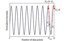
ObjectiveExtrinsic fiber-optic Fabry-Perot (F-P) sensors measure external physical quantities by detecting changes in the interference spectra caused by cavity length variations or refractive index variations within the medium. Compared with traditional sensing technologies, F-P sensors are characterized by high sensitivity, small size, and immunity to electromagnetic interference, and widely employed in the measurement of a variety of external parameters such as pressure, temperature, vibration, displacement, acceleration, and gas. Fiber-optic sensing demodulation technology is an indispensable part of fiber optic sensing systems, which can influence the detection capability of a sensing system to a certain extent, and often needs to meet the requirements of high accuracy and fast calculation speed. Based on this, some demodulation algorithms introduce fast Fourier transform (FFT) as a fast spectrum analysis tool, but how to balance the demodulation accuracy and computational speed has become a major challenge. In our study, an adaptive FFT demodulation algorithm based on white light interference is proposed. Compared with the traditional FFT algorithm, this algorithm combines the efficient computational characteristics of the FFT algorithm and the idea of adaptive sampling length and realizes accurate eigenfrequency calculation by adjusting the spectral sampling length adaptively. Meanwhile, it performs the whole-cycle orthogonal phase-locked detection of spectra to realize accurate phase information extraction, which can improve the demodulation precision during the dynamic signal demodulation. During dynamic signal demodulation, on the one hand, the demodulation accuracy and stability can be improved, and on the other hand, the real-time spectrum refinement process required by the traditional FFT cavity length demodulation method under the dynamically changing cavity length can be avoided. Additionally, the phase demodulation accuracy can be significantly improved, with fast signal demodulation ensured.MethodsWhite light interference technology is employed to obtain the interference spectrum of the F-P sensor, and by adopting adaptive adjustment to the spectral sampling length, the maximum number Nmax of whole cycles within the sampling range and the exact value of the eigenfrequency are obtained to meet the conditions of the whole cycle simultaneously. Meanwhile, this can ensure that the signal demodulation of the noise spectral level is not affected, thus achieving the sensing signals of the low-noise, high-precision, fast signal demodulation. We also utilize theoretical analysis and numerical simulation to analyze the effects of signal amplitude, signal frequency, sensor cavity length, and initial phase on the signal demodulation performance of the adaptive FFT demodulation algorithm by adopting the control variable method and comparing it with the traditional FFT. Compared with the traditional FFT scheme, the adaptive FFT demodulation algorithm can improve eigenfrequency calculation accuracy, and reduce the noise, relative amplitude error Km of the fundamental frequency signal, and total harmonic distortion (THD). The ability of the adaptive FFT algorithm to demodulate the superposition spectra of the multiplexed array is also simulated, showing strong suppression capability of fundamental frequency crosstalk (FFC).Results and DiscussionsAs the signal amplitude increases, the relative amplitude error of the base frequency signal of the adaptive FFT demodulation algorithm is basically maintained near 0, and the fluctuation at the lower amplitude is much smaller than the FFT demodulation result, which realizes more stable and more accurate signal demodulation. As the signal amplitude rises, the two demodulation algorithms show distortion at the same time, but the THD of the adaptive FFT demodulation result is always lower than that of the traditional FFT demodulation result (Fig. 2). Additionally, the stability of the adaptive FFT demodulation algorithm is much higher than that of the traditional FFT, and when the first phase changes, the relative amplitude error fluctuation of the fundamental frequency signal is only 1/40 of that of the traditional algorithm. Meanwhile, the THD is 25 dB lower than that of the traditional FFT (Fig. 4), which greatly improves the signal demodulation stability and accuracy. At the same time, the adaptive FFT also shows excellent cavity length adaptability, and with the changing cavity length, the eigenfrequency estimation error is only 10-4. Compared with the traditional FFT, the computational accuracy has been improved by nearly ten times, the noise level has been reduced by about 2 dB, and the variation of noise level with the cavity length fluctuation is only 1 dB, which is 1/3 of the fluctuation of the traditional FFT algorithm (Fig. 5). What’s more, the relative amplitude error fluctuation of the demodulated fundamental frequency signal of the FFT algorithm is about 0.6 dB, 12 times the amplitude error fluctuation of the demodulated fundamental frequency signal of the adaptive FFT algorithm. The THD of the adaptive FFT demodulation result is 10?20 dB lower than that of the traditional algorithm with smaller fluctuation amplitude, which demonstrates higher accuracy and cavity length adaptability (Fig. 6). In multiplexed system simulation, the adaptive FFT then shows stronger crosstalk suppression capability, reducing the FFC by about 20 dB (Fig. 7).ConclusionsWe propose an adaptive FFT demodulation algorithm for white light interference and conduct simulations and analysis to verify the demodulation performance of the algorithm. The demodulation algorithm adaptively adjusts the sampling length according to the eigenfrequency of the F-P sensor, improves the eigenfrequency estimation accuracy, and realizes the whole period calculation of the periodic white light spectrum. Additionally, this can reduce the phase-locking calculation error in the phase demodulation algorithm, and improve the demodulation adaptability and demodulation stability of the demodulation algorithm for the F-P cavities of different cavity lengths. Simulation comparison shows that the adaptive FFT demodulation algorithm is better than the FFT demodulation algorithm in terms of demodulation accuracy, demodulation stability, and cavity length adaptation range. This algorithm can also be stably applied to sensors with different cavity lengths in different external environments, thus providing a more reliable and effective signal demodulation method for the fiber optic F-P sensors in various application scenarios. Meanwhile, it can be very well applied to small-sized sensor arrays and high-precision and low-noise sensor arrays. At the same time, the adaptive FFT can accurately identify the frequencies corresponding to all the peaks in the spectra, demodulate the superposition spectra of multiplexed arrays, and reduce the inter-channel crosstalk, which is expected to be applied to the signal demodulation of large-scale extrinsic fiber-optic F-P sensing arrays.
Nov. 20, 2024Vol. 44 Issue 22 2204001 (2024)
Jun Zhang, Wenjun Yang, Lei Li, Xiaoran Zhang, and Yabin Zhu
ObjectiveIn recent years, with the development of nanotechnology, research on vanadium dioxide (VO2) microstructures focuses on preparation, property control, and application, particularly in areas such as smart windows, storage devices, and optoelectronic devices. The light field control performance of VO2 microstructures has shown great potential in fields like photocatalysis, optical sensing, and optoelectronic devices. Currently, the mainstream preparation methods include solution methods and thermal decomposition methods, but they have drawbacks such as complex processes. We employ a self-assembly method to prepare tungsten-doped VO2 microstructures and thoroughly explore their light field control performance to achieve practical applications.MethodsA homemade circular polystyrene (PS) mold with a diameter of 10.0 mm and a thickness of 2.0 mm is placed on a clean and level desk. Adhesive tape is applied on the desktop beneath and above the mold, and the polyethylene (PE) lines are cut into long and short threads, which are then interlaced densely on the mold and fixed at both ends with tape. After securing the mold, it is flipped, and two drops of nanosolution with a W-doped atomic ratio of 2% are dripped from 1 to 2 cm above the mold, waiting for it to solidify. Once solidified, the long thread is carefully separated from the microstructure, leading to WxV1-xO2/glass microstructures under different numbers of PE lines. Finally, the sample made with nanosolution with a W-doped atomic ratio of 2% and 9 PE lines exhibits sound symmetry, clarity, integrity, and uniformity. The above experiment is repeated by utilizing WxV1-xO2 nanosolution with a W-doped atomic ratio of 2% and 9 PE lines, with the formation process of the WxV1-xO2/glass microstructure recorded. The solution first spreads outward to the edges of the homemade experimental mold, with the relatively thin center of the solution and relatively thick edges. The PE lines form symmetrical crescent-shaped films, which gradually thicken inward. Subsequently, the surface morphology of the film samples is tested by adopting the German ZEISS GeminiSEM 300 scanning electron microscope. Then, a testing platform is set up by employing a 980 nm wavelength laser, with the optical path shown in Fig. 4. Thermal-sensitive paper is adopted to help align the optical path, ensuring that the laser passes through the film. Meanwhile, a helium-neon (He-Ne) laser is utilized to replace near-infrared light to assist in observing diffraction patterns.Results and Discusses On the set-up near-infrared light transmittance measurement device, by replacing the light detector with a screen and the infrared light with a He-Ne laser, distinct moiré patterns can be observed for the nine vertically aligned WxV1-xO2/glass microstructures. After appropriately adjusting the relative position of the light-emitting device and the VO2 microstructure, the moiré patterns can be observed. By keeping the horizontal distance between the light source and the microstructure unchanged, and adjusting the vertical relative position of the light source and the WxV1-xO2/glass microstructure, it is possible to observe whether moiré patterns form. Additionally, the vertical adjustment between the light source and the WxV1-xO2/glass microstructure is achieved by utilizing the LD-60-CM (XYZ-axis) high-precision manual displacement stage. For the cross and asterisk VO2 microstructures, the diffraction fringes can be observed to change as the relative vertical position between the light source and the WxV1-xO2/glass microstructure is altered. Meanwhile, the diffraction patterns show two types of stripes intersecting to form a cross at times and alternating patterns at other times. Based on the diffraction patterns of the cross and asterisk WxV1-xO2/glass film microstructures under red laser light, we can observe that compared to the patterns of the 9 WxV1-xO2/glass thin film microstructures under visible light, both the cross and asterisk WxV1-xO2/glass microstructures show intersecting grid patterns, which are moiré patterns produced by the grating superposition. Computer simulation of moiré patterns is realized by adopting Python code. The transmittance data of different WxV1-xO2/glass thin films and microstructures at different temperatures are obtained via a variable-temperature infrared testing platform.ConclusionsWe innovatively fabricate the WxV1-xO2/glass thin film microstructure by employing a simple and feasible method of mold preparation. By observing and testing the optical properties of the WxV1-xO2/glass microstructure, we conclude that the sample with a W-doped atomic ratio of 2% has better formation and light field control performance. Furthermore, cross and asterisk microstructures are designed, and a He-Ne laser is adopted as the light source to obtain diffraction patterns. After light passes through the WxV1-xO2/glass microstructure, diffraction phenomena occur, and it is observed that within a certain range, adjusting the relative position of the light source to the vertical direction of the microstructure allows the observation of changes in the diffraction pattern of the microstructure. A self-built variable-temperature infrared testing platform is adopted to achieve control of the diffraction pattern direction, and the computer simulation of the moiré patterns generated by the grating superposition is consistent with the experimental results. This demonstrates that the optical properties of the W-doped VO2 microstructure prepared by a simple, low-cost, and easy-to-implement method can be quantitatively controlled. We will focus on developing devices that can finely control the light field control performance of the WxV1-xO2/glass microstructure in subsequent studies to achieve industrial applications.
Nov. 19, 2024Vol. 44 Issue 22 2205001 (2024)
Xiaoyu Lu, Hui Yang, Haiyang Luo, Anlin Yi, and Lianshan Yan
ObjectiveOptical performance monitoring is crucial for enhancing the reliability and intelligence of optical communication networks. Chromatic dispersion (CD) monitoring is essential for adaptive, precise dispersion and nonlinear compensation in dynamic optical networks, where even small errors can significantly affect receiver performance. Traditional CD monitoring methods, which typically rely on clock phase information, autocorrelation functions, signal peak-to-average ratios, and signal amplitude and phase information, operate primarily in the time or frequency domains. However, these approaches often overlook information in joint time-frequency domain distributions and are generally limited to a monitoring range within 1000 km. The fractional Fourier transform (FrFT), an extension of the traditional Fourier transform, provides flexible analysis and extraction of time-frequency domain features by adjusting the transform order. While FrFT-based schemes can improve the range of dispersion monitoring, they typically suffer from monitoring errors above 100 ps/nm. In this study, we propose a chromatic dispersion monitoring scheme that uses an inverse Radon (iRadon) transform with large angular intervals to improve accuracy. Our approach effectively reduces noise interference and enhances subtle variations in time-frequency maps, increasing sensitivity to dispersion changes and reducing the complexity of network parameters.MethodsWe introduce a training sequence processed by FrFT into the transmitted signal for dispersion monitoring. This sequence can be generated by applying a fixed-angle FrFT to the DC signal. At the receiver, the received signal is downsampled, and the training sequence is processed through FrFT to obtain a two-dimensional time-frequency map. A cubic operation is then performed on this map to emphasize the energy peak position and mitigate the influence of nearby linear components. The iRadon transform is then applied to convert the two-dimensional time-frequency map from polar to Cartesian coordinates. Unlike traditional iRadon transform schemes that use small angular intervals, we propose a discrete iRadon transform with large angular intervals. This approach enhances peak shifts and increases the sensitivity of the time-frequency map to changes in dispersion characteristics. Using a 20° angle interval as an example, we demonstrate the effectiveness of the proposed scheme in improving the dispersion monitoring accuracy. The features extracted from the iRadon transform at large angular intervals are then fed into a lightweight convolutional neural network (CNN) for cumulative dispersion monitoring.Results and DiscussionsThe results show that, for a dispersion monitoring range of 1600?24000 ps/nm, the proposed scheme consistently achieves monitoring errors below 30 ps/nm, with a mean absolute error (MAE) of 19.82 ps/nm. This represents a significant improvement over the maximum residual cumulative dispersion value of 350 ps/nm that can be compensated by the constant mode algorithm (CMA). Compared to traditional FrFT methods with small angle interval iRadon transforms, the monitoring performance is improved by a factor of four. The enhanced dispersion monitoring function, which focuses on the height variation between linear components in the time-frequency map, enables the lightweight CNN to achieve high-precision dispersion monitoring. Notably, the CNN in the proposed scheme requires only 15960 training parameters, compared to 6653703 in traditional methods. In addition, we explore the influence of different signal-to-noise ratios (OSNR), transmission power levels, and differential group delay (DGD) on dispersion monitoring in fiber optic links. We find that when the OSNR exceeds 19 dB, the dispersion monitoring error is kept within 50 ps/nm for transmission distances up to 800 km. As the OSNR decreases, the monitoring error increases. When the input optical power ranges from -2 to 2 dBm, the nonlinear effects are weak, and the dispersion monitoring error remains below 100 ps/nm. However, as the power increases, the nonlinear effects intensify, leading to a gradual increase in the monitoring error. Finally, we analyze the influence of DGD on the dispersion monitoring accuracy, with OSNR set to 30 dB and DGD varying from 0 to 50 ps in 10 ps increments. We observe that for DGD values between 0 and 40 ps, the overall error remains small, with a maximum error of -133.81 ps/nm at 40 ps, indicating robust performance against DGD variations within this range. However, when DGD reaches 50 ps, the overall prediction error deviates significantly from the centerline, with the maximum monitoring error reaching -319.99 ps/nm.ConclusionsIn this study, we propose a novel CD monitoring scheme based on the large angle interval iRadon transform. The approach effectively suppresses noise, enhances dispersion sensitivity, and reduces the required neural network parameters, achieving high-precision and low-complexity CD monitoring. Simulation results demonstrate that for accumulated chromatic dispersion values ranging from 1600 to 24000 ps/nm, the proposed scheme achieves an MAE of 19.82 ps/nm. This represents a more than fourfold improvement in accuracy and a two order-of-magnitude reduction in neural network parameters compared to the FrFT method with small angle interval iRadon transform.
Nov. 19, 2024Vol. 44 Issue 22 2206001 (2024)
Qizhen Song, Feng Liu, Yanbo Yang, Wenxiang Zhang, Ziye Wu, Zhuoqi Li, Zhibin Li, Pengpeng Fan, Jieyuan Tang, Wenguo Zhu, Huadan Zheng, Yongchun Zhong, Zhe Chen, and Jianhui Yu
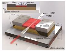
ObjectiveWith the rapid advancement of science and technology, the demand for precise electric field measurements is increasing across fields such as electric power, communication, industrial automation, and biomedicine. In real-world applications, electric field sensors often face complex and variable environmental conditions, including temperature fluctuations and electromagnetic interference. Traditional electric field sensors frequently struggle to meet high-precision measurements, but sensors based on micro-nano tapered two-mode fibers (TTMFs) combined with a disperse red 1/polymethyl methacrylate polymer (DR1/PMMA) offer a promising solution for achieving high-precision measurements. In this paper, we aim to develop and validate a novel all-fiber electric field sensor, leveraging the combination of TTMF’s sensitivity and the exceptional electro-optic properties of the DR1/PMMA. The primary objective of this research is to design an electric field sensor with high sensitivity, fast response, low temperature sensitivity, and excellent stability. The TTMF’s dual-mode interference effect, paired with its unique geometry, provides high sensitivity. The all-fiber structure simplifies the sensor fabrication process and enables seamless integration with other fiber optic devices, significantly facilitating the construction of complex fiber-optic sensing networks while reducing system integration challenges and costs. When combined with DR1/PMMA, the sensor exhibits significant output signal changes even with minor variations in the electric field, making it highly suitable for high-precision measurement scenarios. In addition, DR1/PMMA’s picosecond-level response speed allows the sensor to rapidly detect dynamic electric field changes, providing robust technical support for real-time monitoring and applications with high real-time demands. Unlike traditional liquid crystal (LC)-based electric field sensors, DR1/PMMA-based sensors are largely insensitive to temperature changes, which enhances their stability and reliability in diverse environmental conditions while minimizing measurement errors caused by ambient temperature fluctuations.MethodsFor the material selection, we choose DR1/PMMA film as the electro-optic material due to its excellent electro-optic effect, allowing its refractive index to vary with the applied voltage. Tapered optical fibers are chosen as the sensing elements due to their low loss, strong evanescent field, miniaturized size, and high sensitivity, making them ideal for constructing highly sensitive sensors. We apply electropolarization to the DR1/PMMA film to enhance its electro-optic coefficient, a critical factor for achieving high electric field sensitivity. The tapered waist region of the TTMF is then integrated onto the surface of the electropolarized DR1/PMMA film, ensuring close contact between the fiber and the film to maximize light-polymer interaction. In the tapered region of the TTMF, modal interference occurs between higher-order modes and the fundamental mode. Since the refractive index of the DR1/PMMA film changes with applied voltage, this causes a modulation of the transmitted light within the fiber, leading to a shift in the interference pattern or a change in light intensity at a specific wavelength. To evaluate the sensor’s performance, we construct an experimental setup, integrating the TTMF with the electropolarized DR1/PMMA film, and apply different voltages to observe the optical field modulation effect. Simulation software is also used to model the sensor structure, verifying its working principles and performance characteristics.Results and DiscussionsIn this paper, we propose several key innovations. Firstly, the all-fiber structure design significantly reduces the interference from external electromagnetic coupling, allowing the sensor to maintain high precision in complex electromagnetic environments and enhancing system stability and reliability. Secondly, the compact size of the device facilitates portability and deployment, enabling its use across a broader range of scenarios. The sensor’s optical signal modulation capability ensures high-speed signal transmission, shortening response time and enhancing electromagnetic interference resistance. This makes it ideal for capturing electric field changes in environments with strong electromagnetic fields. The sensor’s design exhibits excellent sensitivity and low signal distortion, crucial for high-precise applications such as monitoring electric fields in medical equipment or troubleshooting precision electronics. Structurally, the sensor is straightforward and easy to fabricate, reducing production costs and simplifying maintenance. Notably, the use of DR1/PMMA, an organic electro-optic polymer, provides both ease of processing and molding, along with a high electro-optic coefficient, forming a solid material foundation for high-sensitivity sensing. In addition, the innovative use of TTMF as the modal interferometer substrate fully exploits the characteristics of tapered fibers, such as low loss, strong evanescent fields, and compact size. The design also strengthens the fiber’s mechanical resilience, reducing the risk of damage from external forces and further enhancing the durability and longevity of the sensor.ConclusionsIn this paper, we propose an innovative all-fiber electric field sensor architecture by integrating a highly sensitive TTMF with a DR1/PMMA electro-optic film. The core of the design is the DR1/PMMA film, which boasts a remarkable electro-optic coefficient of 3.68 pm/V, providing a strong foundation for the sensor’s performance. By utilizing the high refractive index sensitivity (8154.76 nm/RIU) of the DR1/PMMA film, we have achieved a sensor design capable of rapid and highly sensitive electric field detection. Experimental validation demonstrates that the sensor’s impressive electric field sensitivity of 0.86 dB/V, along with a 3 dB bandwidth of 1.4 kHz, enabling broad signal transmission coverage. In addition, the sensor effectively limits harmonic distortion to less than 2.5% in the AC electric field range of 1 to 5 kHz, ensuring high-fidelity signal transmission. Looking ahead, applying the proposed structure and fabrication methods to other polymers with high electro-optic coefficients opens up new possibilities for creating high-performance fiber-optic electric field sensors.
Nov. 19, 2024Vol. 44 Issue 22 2206002 (2024)
Qiufeng Shang, Xiaokai Fan, Yuanyu Gu, Jianjian Wang, and Guozhen Yao
ObjectiveReal-time monitoring and evaluation of transmission lines are essential to ensure the safety and stability of the power grid. Phase-sensitive optical time domain reflectometry (Φ-OTDR) offers advantages such as long detection range, strong resistance to electromagnetic interference, and low cost. It can directly utilize redundant fibers in optical fiber composite overhead ground wire (OPGW) and can effectively determine the operational status of transmission lines. This technology has broad application prospects in the field of transmission line status monitoring. Currently, the commonly used signal recognition methods in optical fiber vibration sensing are primarily based on machine learning and deep learning. In traditional machine learning, signal features are often extracted based on human experience before being input into a classifier, meaning that recognition performance is heavily dependent on the selection and quantity of these features. Deep learning, however, can automatically extract and select useful features from raw data, reducing the influence of manual intervention on recognition accuracy. Nonetheless, most existing deep learning methods primarily analyze a single mode of the vibration signal, limiting the model’s ability to fully extract effective feature information. To more comprehensively describe signal characteristics and improve model recognition performance, we propose a transmission line signal recognition method that integrates one-dimensional time-domain signal analysis with two-dimensional image signal analysis, using a dual-branch convolution neural network (CNN) structure and a multi-attention mechanism. Six types of on-site data from transmission lines under different operating environments are collected using the Φ-OTDR system to construct a dataset for algorithm verification. The proposed method’s recognition rate is compared with five other deep learning models, and the recognition performance of machine learning and deep learning methods on large-scale datasets is also analyzed.MethodsIn this model, the time-sequence branch uses a one-dimensional convolutional neural network (1DCNN) to directly extract temporal features from the raw vibration signal, while the image branch uses continuous wavelet transform (CWT) to convert the vibration signal into a two-dimensional time-frequency image, which is then processed by a two-dimensional convolutional neural network (2DCNN) to learn the time-frequency features of the image. To enhance the focus on critical information, channel attention mechanisms are incorporated into both branches. The proposed branch attention mechanism effectively addresses the issue of insufficient recognition accuracy caused by differences in modal information during feature fusion by assigning weights to branch features. Parameter comparison experiments are conducted to select the appropriate wavelet function for the dataset, comparing the effects of different wavelet functions on final recognition accuracy (Fig. 8). In addition, ablation experiments are designed to verify the effectiveness of the attention mechanism included in the algorithm (Fig. 9). The proposed method is also compared with five deep learning models: single branch 1DCNN, single branch 2DCNN, 1DCNN-LSTM, 1DCNN BiLSTM, and ATCN-SA BiLSTM. Furthermore, it is compared with three common machine learning methods: SVM, KNN, and decision tree. Before being input into the machine learning classifier, the six types of vibration signals are decomposed using variational mode decomposition with seven layers, and features are extracted for each decomposed modal component, resulting in four datasets with different features (Table 7).Results and DiscussionsIn the parameter comparison experiment, the model achieves the highest recognition accuracy for the time-frequency image data set using the Morlet wavelet function (Fig. 8, Table 4). In the ablation experiments, the model without the added attention mechanism has the lowest recognition accuracy, while our method, which includes channel and branch attention mechanisms, achieves the highest recognition accuracy by enabling the model to focus on key information (Fig. 9, Table 5). The recognition performance is measured by comparing the accuracy, precision, recall, and F1 scores of different deep learning models on the test set (Fig. 10, Fig. 11, Table 6). The results demonstrate that the proposed method, by integrating two different types of modal information, compensates for the limitations of one-dimensional vibration signal and two-dimensional image data, providing a more comprehensive description of data characteristics. The classification accuracy on the test set reaches 94.92%, and the overall evaluation indices are optimal. In addition, a comparison between 1DCNN and 2DCNN shows that 2DCNN offers a modest improvement in recognition accuracy and a slight advantage in convergence speed, suggesting that converting one-dimensional signals into two-dimensional images can improve recognition performance to some extent. In the comparison experiment with machine learning methods, the machine learning methods are trained and tested using the extracted four feature datasets (Fig. 12). The results show that the recognition performance of the machine learning method is significantly affected by the type and number of extracted features, and their recognition accuracy is far lower than that of our method, highlighting the insufficient generalization performance and classification efficacy of machine learning algorithms when processing large-scale datasets.ConclusionsTo address the challenge of real-time monitoring of transmission line operational status, we propose a deep learning model based on a dual-branch CNN structure and multi-attention mechanism. The model’s time-sequence branch extracts time-domain features from vibration signals, while the image branch extracts time-frequency features from two-dimensional images. Channel and branch attention mechanisms are incorporated to enhance the model’s focus on key feature information. On a real transmission line vibration signal dataset, the proposed method achieves a recognition accuracy of 94.92%, outperforming single branch networks, 1DCNN-LSTM, 1DCNN-BiLSTM, and ATCN-SA-BiLSTM models. When handling large-scale datasets, the proposed method demonstrates superior generalization and recognition performance compared to machine learning methods. The method provides a valuable reference for monitoring the operational conditions of transmission lines.
Nov. 20, 2024Vol. 44 Issue 22 2206003 (2024)
Qingxiang Li, Haiyan Liu, Yihui Chen, Yi Cheng, Qianqian Luo, and Zhengpeng Li
ObjectiveThe exponential growth of indoor mobile traffic and data connections has led to an increasing demand for indoor positioning. Since satellite-based positioning systems like GPS and Beidou face significant limitations indoors due to signal attenuation and blockage, it is crucial to find a high-accuracy, low-cost indoor positioning solution. Visible light positioning (VLP) has emerged as a strong candidate for indoor positioning due to its low cost, high accuracy, lack of electromagnetic interference, and ability to simultaneously support communication, positioning, and illumination. Currently, VLP technologies based on photodetectors (PDs) have been widely studied and applied because of their low cost and ease of implementation. These systems typically estimate user coordinates through various positioning algorithms, such as time difference of arrival (TDOA), angle of arrival (AOA), received signal strength (RSS), and RSS fingerprinting with artificial neural networks (ANNs). However, these methods often assume that light sources are vertically aligned and the PD is positioned horizontally. In dynamic scenarios where the PD is randomly tilted, positioning can degrade. To address this issue, researchers have proposed a hemispherical lamp with multi-directional LEDs (MD-LEDs) and a positioning algorithm based on the RSS ratio (RSSR). While this method can accommodate tilted PDs, the hemispherical lamp structure is difficult to implement, and the algorithm details are not fully disclosed. To overcome these limitations, other researchers have developed the first prototype of a multi-directional LED integrated lamp, introducing the RSSR-based linear least squares (RSSR-LLS) algorithm. Experimental results show that the average localization error (LE) of the RSSR-LLS algorithm is about 11 cm when the PD is tilted in a relatively open environment. To further enhance the positioning performance of the MD-LED-aided VLP (MD-VLP) system, we propose a new approach using a neural network (RSSR-ANN) based on the RSSR method. Extensive simulations and experiments confirm that this new method achieves the desired performance improvements.MethodsIn this study, we propose an RSSR-ANN scheme for the MD-VLP system. This approach utilizes a single PD to capture light intensities from multiple LEDs oriented in different directions, then feeds the RSSR values between pairs of LED intensities into a trained artificial neural network model to predict plane coordinates. Specifically, a feed-forward backpropagation neural network model with three hidden layers is constructed, including an input layer, hidden layers, and an output layer (Fig. 2). The RSSR values from known positions are used as input, and the corresponding plane coordinates serve as output. Model training is performed using gradient descent and backpropagation to determine the weights and biases, resulting in the final target model. Once the ANN model is established, it can predict the user’s plane coordinates by processing the RSSR values received by the PD. The neural network can automatically extract features from vast amounts of data and adjust the network weights iteratively through its multi-layer hidden structure, effectively fitting nonlinear data. Therefore, the method also supports MD-VLP systems using non-Lambertian radiation LEDs.Results and DiscussionsTo verify the universality of the proposed scheme, we simulate and analyze the positioning performance of the MD-VLP system using LEDs with different radiation patterns (Fig. 4). MATLAB software is used to simulate PDs receiving signals from multi-directional LEDs, generating RSSR values at various coordinates. These values are then fed into a Pytorch?-based ANN model for training. Once trained, test data are used to evaluate the model’s performance. Simulation results demonstrate that when using two types of non-Lambertian radiation LEDs, the average LE achieved is 3.70 cm and 6.22 cm, respectively, even with moderate PD tilting (Fig. 5). In addition, we conduct a series of experiments using both MD-LED integrated lamps with standard Lambertian LEDs and a VLP device consisting of commercially available LED downlights to validate the generalizability of the proposed scheme (Fig. 6). Experimental results indicate that the average LE is 2.96 cm when the PD is horizontal and 5.51 cm when tilted at 15° (Fig. 8), a significant improvement over the RSSR-LLS algorithm. Furthermore, we investigate the positioning performance of the RSSR-ANN scheme in a random reflection environment, where reflective objects like tables and chairs are arranged around the PD to alter the illuminance distribution. Results show that the scheme achieves an average LE of 6.02 cm even when the PD is horizontal.ConclusionsSeveral key conclusions can be drawn from the simulation results. First, the proposed RSSR-ANN scheme is suitable for MD-LED integrated lamps using standard Lambertian radiation LEDs as well as non-standard Lambertian LEDs. Second, the MD-VLP system can utilize non-Lambertian radiation LEDs, as long as the radiation curve remains monotonic within the angle range [0°, θm], where θm is the maximum radiation angle. Finally, the ANN model trained with a horizontal PD still supports positioning when the PD is randomly tilted. Compared to the RSSR-LLS algorithm, the RSSR-ANN scheme increases average LE by 40%. Experimental verification further demonstrates that the proposed scheme is effective in systems using both standard and non-standard Lambertian LEDs, enhancing the overall universality of the MD-VLP model. In addition, the RSSR-ANN scheme performs well in dynamic scenarios with randomly tilting PDs, improving LE performance by 52.5%?72.3% under various conditions (Table 4). This suggests that the MD-VLP system based on RSSR-ANN holds great potential for mobile applications.
Nov. 20, 2024Vol. 44 Issue 22 2206004 (2024)
Xiaohan Wang, Liqun Huang, Yuhao Wang, Hongwei Yang, and Shunshun Liu
ObjectiveWith the continuous development of new services such as the Internet of Things, cloud computing, 5th generation mobile communication, artificial intelligence, and virtual reality, a large number of terminal devices are connected to the network, and the required transmission capacity is increasing exponentially, which puts forward higher requirements for optical fiber communication systems. The core idea of probabilistic shaping (PS) is to both increase the sending probability of the inner constellation points and reduce the sending probability of the outer constellation points. This technology can improve the bit error rate performance and spectral efficiency of the optical fiber communication system, and make the channel capacity approach the Shannon limit. As PS is flexible, efficient, and easy to combine with other technologies, it is considered to be one of the key technologies in the future ultra-long distance, ultra-large capacity, and ultra-high speed optical fiber communication system. Since PS algorithms with low computational complexity are undoubtedly easier to implement in high-speed optical fiber communication systems, they have high research significance, especially for passive optical networks which require more low-cost solutions.MethodsA PS algorithm of group inversion based on symbol-level label is proposed to realize PS of quadrature amplitude modulation (QAM) signals by inverting the data bits after grouping. According to different inversion rules, two methods of information bit inversion (IBI) and outer constellation point inversion (OCPI) can be divided. IBI is inverse according to the code weight after grouping, and an approximate gray-coded mapping rule is designed to let more constellation points with a small code weight in the inner circle and thus improve the shaping effect. OCPI takes the inverse operation according to the rule that the code group mapped by the outer and inner constellation points is exactly the inverse code. In the optical orthogonal frequency division multiplexing (OOFDM) system, the effects of different code group lengths (m) and inverse thresholds (n) are simulated. The results show that the algorithm not only features low complexity and high coding efficiency but also obtains a better shaping effect and improves the bit error rate performance of the system. Finally, the PS algorithm of group inversion combining hierarchical modulation (HM) technology further improves the performance of the system and gives it service classification advantages.Results and DiscussionsSince the PS algorithm of group inversion based on symbol-level label only needs the one-bit length of labels and does not need to establish a lookup table to achieve PS, it has low computational complexity and is easy to implement. The algorithm is successfully applied to the PS of 16 QAM and 32 QAM. Controlling the length of m can help flexibly strike a balance between coding efficiency and PS gain. The algorithm is combined with the HM technology, PS is only achieved in the low priority (LP) layer data, and the label bit is placed in the high priority (HP) layer with a low bit error rate, which further improves the coding efficiency and bit error rate performance of the system. Under the coding efficiency of 94.4% (Table 2), the hierarchical modulated 64 QAM can obtain a PS signal-to-noise ratio (SNR) gain of 1.3 dB (Fig. 12).ConclusionsThe IBI and OCPI are proposed according to different inverse rules. Conducting the simulation analysis of the different values of n and m in the proposed algorithm helps indicate that the best shaping effect can be obtained when the optimal inverse threshold is half of the m. Additionally, the smaller m results in lower coding efficiency, better bit error rate performance, and better PS effect. The proposed PS algorithm of group inversion is characterized by low computational complexity, high coding efficiency, wide application range, high flexibility, hardware resource conservation, and easy implementation. Meanwhile, it has broad application prospects and provides an effective solution for the performance improvement of communication systems.
Nov. 19, 2024Vol. 44 Issue 22 2206005 (2024)
Li Zeng, Xiaoyan Sun, Xinran Dong, Youwang Hu, and Ji’an Duan
ObjectiveOptical fiber sensors are a significant branch in the sensor field due to their compact structure, remote monitoring capabilities, and resistance to electromagnetic interference. As sensor technology advances and application demands increase, there is a growing need to monitor multiple parameters simultaneously. For instance, in marine ecological monitoring and the petrochemical industry, simultaneous measurement of strain, temperature, and refractive index is essential. Using single or dual-parameter sensors requires deploying multiple different sensors, which complicates the sensing system. Existing optical fiber sensors typically measure only two parameters, and three-parameter sensors are rare and complex, posing challenges for simultaneous multi-parameter measurement in complex environments. Therefore, designing a compact and flexible three-parameter sensor for simultaneous measurement of strain, temperature, and refractive index is both significant and promising. In this paper, we propose a hybrid structure fiber sensor that integrates a tapered phase-shifted Bragg grating and a Mach?Zehnder interferometer. By leveraging the complementary sensing characteristics of these two components, the sensor can simultaneously measure strain, temperature, and refractive index, offering a novel solution for multi-parameter measurement scenarios in environmental monitoring and the petrochemical industry.MethodsThe hybrid sensor utilizes the complementary sensing characteristics of the tapered phase-shifted Bragg grating and the Mach?Zehnder interferometer to simultaneously measure strain, temperature, and refractive index. The sensing principles for strain and temperature of the tapered phase-shifted Bragg grating and strain and refractive index of the Mach?Zehnder interferometer are analyzed, demonstrating their complementary nature. A Mach?Zehnder interferometer based on multimode fiber (MMF) and photonic crystal fiber (PCF) is constructed. The influence of PCF length on the spectrum is tested to determine the optimal length. The tapered phase-shift grating is fabricated using arc discharge from a fusion welding machine, with precise control of the minimum radius to enhance strain sensitivity while maintaining structural strength. Silver deposition is used on the fiber end face to enable reflective monitoring, reducing sensor length and easing device layout. Finally, a sensing test system for strain, temperature, and refractive index is established, and the performance of the three parameters is evaluated. The matrix method is used to eliminate cross-sensitivity between the parameters, enabling simultaneous measurement.Results and DiscussionsThe reflection spectrum of the sensor is monitored using a spectral analyzer and a broadband light source. After tapering the initial fiber Bragg grating (FBG), a transmission window is created in the middle of the reflection peak (Fig. 2). The spectral change in this window characterizes the response of the tapered phase-shifted grating to strain and temperature, while the intensity change at 1560 nm indicates the Mach?Zehnder interferometer’s response to refractive index and strain. Strain sensing experiments show that with strain increasing from 0 to 300 με, the central wavelength shift of the conical PS-FBG transmission window is 0.59 nm, with a reflection peak intensity difference of 6.42 dB, corresponding to strain responses of 1.88 pm/με and 0.0213 dB/με. The intensity change at 1560 nm is -0.664 dB, with a sensitivity of 0.0022 dB/με (Fig. 4). Temperature experiments show no change in the phase shift of the phase-shifted grating as the temperature rises from room temperature to 120 ℃, with a wavelength modulation temperature sensitivity of 12.2 pm/℃ and an MZI temperature sensitivity of 0.0014 dB/℃ (Fig. 5). Refractive index experiments demonstrate no change in the conical PS-FBG spectrum as the refractive index increases from 1.3330 to 1.3707, with an MZI refractive index sensitivity of -344.81 dB/RIU (Fig. 6). The sensor exhibits good linearity in strain, temperature, and refractive index measurements across the experimental range.ConclusionsA hybrid structure fiber three-parameter sensor based on a tapered phase-shifted Bragg grating and an MZI has been proposed and experimentally validated. The tapered PS-FBG is created through arc discharge, and the MZI is constructed using MMF and PCF. These components are cascaded and silver-plated on the end face. By leveraging the advantages of the tapered PS-FBG for strain and temperature sensing and the MZI for refractive index sensing, the sensor achieves simultaneous measurement of strain, temperature, and refractive index. Experimental results indicate that the sensor’s temperature sensitivity is 12.2 pm/℃, strain sensitivity is 0.0213 dB/με, and refractive index sensitivity is -344.81 dB/RIU, all demonstrating good linearity. The proposed hybrid structure sensor offers a compact design, low manufacturing cost, and flexible use, making it a valuable tool for various applications.
Nov. 20, 2024Vol. 44 Issue 22 2206006 (2024)
Fei Li, and Xiangchuan Gao
ObjectiveVisible light communication (VLC) leverages the visible light spectrum to offer significantly greater bandwidth than radio frequency (RF) communication, addressing RF spectrum congestion and meeting the demands of the Internet of Things (IoT) and future 6G technologies. Typically, multiple light-emitting diodes (LEDs) are installed to meet lighting requirements. By employing multiple input multiple output (MIMO) technology, high data rates and reliability are achieved without additional time and spectrum resources. However, the use of MIMO technology causes overlapping optical signals, resulting in severe multi-user interference (MUI). Transmitter precoding techniques, such as block diagonal (BD) precoding, have been extensively studied as key methods to mitigate MUI. However, due to the high correlation in optical channels, BD precoding suffers from significant disparities in subchannel gains, leading to poor overall bit error rate (BER) performance. Addressing this subchannel gain disparity and mitigating MUI is essential for achieving high-speed, reliable communication.MethodsTo address these challenges, we propose an improved multi-user precoding scheme based on fairness maximization in BD precoding. Building upon the BD precoding’s ability to eliminate MUI and considering VLC’s unique characteristics, we formulate an optimization problem aimed at maximizing the minimum subchannel gain under the constraints of non-negative transmitted optical signals and total transmission power. Due to the non-convex nature of the problem, solving it directly is difficult. To overcome this, we decompose the problem into two independent subproblems: intra-user channel equalization and inter-user power allocation. In the first subproblem, we parameterize the precoding matrix and derive its optimal structure. Then, we use a branch-and-bound algorithm to manage the non-convex constraints, transforming the problem into a mixed-integer constrained convex programming problem. This approach effectively solves the optimal precoding matrix parameters, ensuring that each user’s subchannel gain is maximized. In the second subproblem, we derive a closed-form solution for optimal user power allocation, achieving the goal of maximizing the minimum subchannel gain. This method mitigates the significant subchannel gain disparities in BD precoding and enhances the system’s overall resistance to noise.Results and DiscussionsWe validate the proposed precoding scheme for multi-user MIMO-VLC systems using Monte Carlo simulations. The key parameters of the VLC system are summarized in Table 1. Two scenarios are considered: one with densely clustered users experiencing significant MUI, and another with dispersed users, where MUI effects are less pronounced. We first analyze the effect of the receiver’s field of view (FOV) on BER performance in both scenarios (Figs. 2 and 3). The objective is to identify the optimal FOV that ensures adequate communication coverage while maximizing system performance. These investigations provide reference values for the receiver’s FOV and partially validate the efficacy of the proposed precoding scheme. Across various communication scenarios, the proposed precoding scheme consistently outperforms alternative methods, demonstrating significantly lower BER irrespective of FOV variations. With the optimal FOV determined, we further evaluate the BER performance of the three precoding schemes under different signal-to-noise ratios (SNR) and modulation schemes (Figs. 4 and 5). Under moderate to high SNR conditions, the proposed scheme shows superior BER performance compared with baseline BD precoding. Furthermore, compared to recent nonlinear precoding methods based on geometric mean decomposition (GMD), our scheme delivers comparable BER performance, gradually surpassing GMD-based precoding as SNR increases. It is important to note that GMD-based precoding does not fully address MUI, requiring complex successive interference cancellation at the receiver, which can lead to error propagation. Thus, considering both system performance and receiver complexity, the proposed scheme proves to be a more practical option compared to GMD-based precoding.ConclusionsIn this paper, we propose a fairness-maximized precoding scheme for multi-user MIMO-VLC systems, considering the constraints of non-negative optical signals and total power. This scheme formulates an optimization problem aimed at maximizing the minimum subchannel gain and decomposes this challenging non-convex problem into two independent subproblems: intra-user channel equalization and inter-user power allocation. In the first subproblem, we parameterize the precoding matrix and derive its optimal structure. Using a branch-and-bound method to handle the non-convex constraints, we transform the subproblem into a mixed-integer constrained convex programming problem. This enables the effective determination of the global optimal solution, identifying the unknown parameters of the precoding matrix. The second subproblem derives the closed-form solution for optimal user power allocation, optimizing the system’s overall BER performance. Experimental results demonstrate that the proposed scheme outperforms both baseline BD precoding and GMD-based precoding (from Reference [18]) in terms of BER performance under medium to high SNR conditions. In addition, the complexity at the user receiver is reduced compared to the GMD precoding, making our proposed scheme more suitable for practical engineering applications.
Nov. 20, 2024Vol. 44 Issue 22 2206007 (2024)
Guilong Dai, Jiangfei Huangfu, Xiaoyu Wang, and Yishuo Liu
ObjectiveDecreasing solar radiation reflection loss and re-radiation loss is crucial for improving the thermal efficiency of solar receivers. We propose a mixed particle-packed receiver composed of a modified quartz glass Rasching ring (a short quartz glass tube with both bottom surfaces cut), quartz glass ball, and silicon nitride ball. The modified quartz glass Rasching ring reduces reflection loss by capturing incident solar radiation. In contrast, the quartz glass balls are used to mitigate re-radiation loss from the high-temperature silicon nitride balls. Thus, the values of solar radiation reflection loss and re-radiation loss can be regulated by adjusting the stacking layers of the quartz glass balls, which achieves optimized thermal efficiency for the receivers across different temperature ranges.MethodsThe optical performance of the mixed particle-packed receiver is analyzed using both a particle-scale optical transmission model and experimental measurements. The packing of balls inside the hollow cylinder is simulated with STAR-CCM+ software, and the center coordinates of these balls are thus extracted. Next, the mixed particle-packed receiver model is reconstructed using TracePro software, integrated with a specific optical path system. This system concentrates solar radiation through a parabolic dish mirror and captures the re-radiation emitted from the silicon nitride balls. Solar radiation reflection and re-radiation losses are then simulated with this optical system. Finally, the absorptivity-emissivity ratios and thermal efficiencies are determined for various mixed particle-packed receivers.Results and DiscussionsThe comparison between the simulation and measurement results verifies the reliability of the particle-scale optical transmission model. Results show that the reflection loss of the incident solar radiation increases with the stacking layers of the quartz glass balls. Conversely, the re-radiation loss decreases with more stacking layers. When the tube-to-particle diameter ratio (D/d) is 5, the reflection loss of the R0B5 receiver is nearly 10% higher than that of the R5B0 receiver (Fig. 6), while the re-radiation emissivity of the R0B5 receiver is about 3.7%?9.7% lower than that of the R5B0 receiver across the temperature range of 800?2500 K (Fig. 7). In the mid-temperature range of 500 K to 950 K, the R5B0 receiver exhibits the highest thermal efficiency. In the sub-high temperature range of 950 K to 1525 K, the R4B1 receiver shows the highest thermal efficiency. In the high-temperature range of 1525 K to 2175 K, the R1B4 receiver achieves the highest thermal efficiency. Additionally, in the ultra-high temperature range above 2175 K, the R0B5 receiver delivers the highest thermal efficiency (Fig. 8). Furthermore, silicon nitride particles absorb most of the solar energy (more than 80%), while quartz glass particles absorb only 3.0%?6.5% of the solar energy (Fig. 11).ConclusionsDue to the adjustable optical performance of the mixed particle-packed receiver, the highest thermal efficiency across different temperature ranges can be achieved by altering the stacking layers of the quartz glass balls. The optimized design of the mixed particle-packed receiver offers a novel approach to high-temperature solar receivers, which could be implemented in advanced high-temperature power cycles.
Nov. 20, 2024Vol. 44 Issue 22 2208001 (2024)
Bingzhen Li, Xuan Liu, Zixiang Zhao, Li Li, and Weiqi Jin
ObjectiveAs a key technology for enhancing human visual perception at night, low-level light (LLL) night vision technology has been widely employed in military and civilian fields. Electron bombarded active pixel sensor (EBAPS) as a new generation of LLL night vision imaging devices has become a main research direction in the field of LLL night vision technology due to its low power consumption, high sensitivity, fast response, and excellent performance in extremely low illumination conditions (1×10⁻⁴ lx). To detect and visualize optical signals in extremely low illumination conditions, LLL imaging devices should undergo a series of processes, including photoelectric conversion, signal amplification, and signal reading. However, the application of a series of amplification operations to the signal will inevitably result in noise amplification, which will significantly interfere with the original signal of the image. Therefore, it is vital to study the image denoising of LLL images. Compared to traditional image sensors such as complementary metal oxide semiconductor (CMOS), EBAPS is unique because it adopts bombarded electrons to achieve signal amplification. The signal amplification process in the method may result in a specific noise type, which is referred to as EBS noise in our study. The primary manifestation of EBS noise in the images is randomly distributed, oversaturated, and speckled pixel clusters. Although EBAPS shows great potential in LLL night vision field, the research on its complex mixed noises (EBS noise and Gaussian noise) suppression is still relatively rare. Traditional image denoising methods require highly complex mathematical reasoning and optimization processes while featuring poor performance under complex mixed noises. With the development of technology, deep learning-based image denoising algorithms have been widely adopted in optical imaging, including medical imaging, remote-sensing imaging, and mobile phone photography, due to their powerful feature extraction and excellent modeling capabilities.MethodsDeep learning-based methods are divided into supervised and self-supervised image denoising algorithms based on whether a noisy-clean image-paired dataset is utilized during the training. In many supervised image denoising algorithms, based on limited clean datasets, different noise addition strategies have been employed to obtain noisy images such as additive white Gaussian noise, artificially synthesizing noisy-clean image pairs. However, artificial noise simulation of noise cannot accurately reflect the noise distribution in the objective world. In dealing with noise images in the real world, only relying on the model trained on artificial simulation noise may result in difficulties in yielding the desired denoising effect and accuracy. Therefore, considering that the noise in the EBAPS images is a mixture of EBS and Gaussian noises, the network architecture is designed and divided into two stages. In stage 1, the noise-noise paired dataset is constructed by adopting the iterative strategy and EBS noise, and thus the training phase does not rely on manually adding noise to construct the dataset. Additionally, the U-Net denoising model is built to realize the removal of EBS noise. In stage 2, based on the denoising results of EBS noise, a U-shaped blind-spot net drop model is designed and built for Gaussian noise for training to realize the removal of Gaussian noise.Results and DiscussionsThe experimental data employed in our study are EBAPS images acquired in 1×10⁻⁴ lx and 1100 V experimental conditions. We present a comparison of our algorithm with the benchmark classical denoising algorithms, including BM3D and the advanced self-supervised image denoising algorithms based on deep learning proposed in recent years. For BM3D, B2UB, and DBSN, the adaptability and denoising effect of these methods for EBS noise in EBAPS images are not ideal. However, although AP-BSN and MM-BSN methods can realize EBS noise denoising to a certain extent, they inevitably introduce significant side effects during denoising. This means that the image is over-smoothed, and the details and texture features of the image are lost, thus reducing image clarity and causing visual distortion (Figs. 9?12). In contrast, the proposed method successfully denoises EBAPS images and preserves the details and texture information of the original images. Compared with previous methods, the proposed algorithm yields the optimal performance of PSNR and SSIM, two key evaluation indexes (Tables 1 and 2). The experimental data and intuitive visual effects strongly demonstrate more sound performance and better results of the proposed method than those of current algorithms in targeting EBAPS image noise.ConclusionsWe propose a self-supervised two-stage convolutional neural network model for EBAPS images, which can maximize the preservation of image details and texture information while realizing the denoising of mixed noises (EBS noise and Gaussian noise). Additionally, the proposed method innovatively abandons the traditional practice of expanding the dataset with synthetic noise in the training phase, and instead directly utilizes the inherent noise characteristics of EBAPS images as the dataset. This strategy not only reduces the reliance on synthetic noise but also motivates the proposed denoising algorithm to capture and generalize the complexity of EBAPS image noise more effectively. Our experimental results show that the proposed method achieves better performance than state-of-the-art algorithms on the industry-recognized image quality evaluation metrics PSNR and SSIM. However, there is room for improvement in further optimizing the preservation of image details and simplifying the network structure, which is the main direction of our future research.
Nov. 22, 2024Vol. 44 Issue 22 2210001 (2024)
Xuxia Zhuang, Ningjuan Ruan, Jiuzhe Wei, and Jinping He
ObjectiveWith the continuous advancement of detector technology, devices with high pixel density and small pixel size are constantly emerging. However, as the pixel size of the detector decreases, the signal-to-noise ratio (SNR) of the detector is reduced, which makes it difficult to meet the SNR requirements for imaging in fields such as space remote sensing. Multi-pixel binning can improve the imaging SNR of small-pixel devices but does not improve the modulation transfer function (MTF) of the system. We aim to achieve the efficient application of large-format small-pixel devices in optical imaging and comprehensively enhance the system’s MTF and SNR by researching a new weighted sampling and optimization method.MethodsThe weighted sampling and optimization method for large-format small-pixel optical imaging devices is proposed. The weighted sampling method takes several adjacent pixels as a superpixel, and each pixel within the superpixel is assigned a different weight factor. The weight factor is multiplied by the signal of each pixel, and then the signals after weighting are summed up to form the output of the superpixel. Based on the technical principles, a weighted sampling imaging quality is constructed, which includes MTF and SNR. Meanwhile, the image quality is analyzed under different pixel quantities in a superpixel and various weighted factors. By taking MTF×SNR as the optimization target function, the optimization function for the weight factors is constructed. Meanwhile, boundary constraint conditions are set and a global search method is employed. Within the boundary constraints of the variables, the size of the variables is continuously changed for iteration and optimization, thus achieving the optimal setting of the weight factors. The weighted sampling image simulation experiment is conducted, and image MTF tests are performed based on the edge method. Additionally, the SNR is calculated by employing the ratio of the mean and variance of the gray level in the uniform area, and the experiment results are consistent with the theoretical analysis.Results and DiscussionsThe results indicate that by employing weighted sampling, the overall imaging quality can be improved. Pixel quantities in a superpixel and the weighted parameters are the main influencing factors. Compared to traditional pixel-binning methods, when a 3×3 pixel group is adopted as a single sampling unit, the MTF can be increased up to 1.4 times, and SNR is equal to that of a single pixel. When a 5×5 pixel group is adopted as a single sampling unit, the MTF can rise to 1.5 times, and the SNR is equal to that of a single pixel. Compared to single-small-pixel imaging methods, when a 3×3 pixel group is utilized as a single sampling unit, SNR can be increased up to 3.0 times, MTF is equal to that of a single pixel, and MTF×SNR can rise to 3.1 times. When we employ a 5×5 pixel group as a single sampling unit, SNR and MTF×SNR can increase up to 5.0 times and 5.2 times respectively.ConclusionsWe propose a weighted sampling method and weight factor optimization method based on large-format small-pixel devices. The feasibility of this method is verified by simulation analysis. The proposed method can leverage the advantages of small pixels and high pixel density. Compared to traditional sampling methods, it can comprehensively improve the SNR and MTF of the imaging system. On the other hand, by setting different weight factors, it can meet the needs of different imaging tasks. The results can provide theoretical guidance for new applications of this type of detector. In practice, according to the actual imaging performance requirements, corresponding constraint conditions can be set to design the weight factors.
Nov. 19, 2024Vol. 44 Issue 22 2211001 (2024)
Sen Yu, Zhenru Wang, Lirong Qiu, Jian Cui, and Weiqian Zhao
ObjectiveWith the rapid development of ultra-precision manufacturing, various precision components with micro and nanostructures are widely employed in fields such as engineering materials, biomedicine, optical imaging, and semiconductor manufacturing. Meanwhile, they are developing toward high-performance manufacturing with increasing scale, increasingly fine structures, and increasingly complex structural shapes. Testing techniques and processing techniques complement each other to truly reflect the processing quality of ultra-precision manufacturing devices and study device functions, which is an essential part of the development of ultra-precision manufacturing technology. A laser scanning lateral differential confocal microscope is developed in our study to tackle the challenge of high-speed and high-precision measurement of complex surface morphology of microstructured samples.MethodsFirstly, the emitted laser enters the galvanometer beam scanning module after passing through the splitter prism. The laser emitted from the galvanometer beam scanning module focuses on its focal plane by the scan lens, and the rear focal plane of the scan lens coincides with the rear focal plane of the tube lens. After being collimated by the tube lens, it enters the measurement objective. Finally, the measured objective converges the laser beam on the surface of the sample. By changing the control signal, the laser exits from the two-dimensional galvanometer in different directions, causing the parallel light direction to enter the measurement objective to change accordingly. This changes the lateral position of the light spot that converges on the surface of the sample, forming the measurement beam. Even if the sample is not moved, the laser spot and the measured sample can still be changed by controlling the reflection angle of the galvanometer scanning module. Additionally, the relative position is adjusted to achieve beam scanning. The light beam reflected by the tested sample returns to the original path and passes through the measurement objective, tube lens, scan lens, and galvanometer beam scanning module in sequence. After being reflected by the splitter prism, it forms a detection beam via the collection lens. The system inserts a D-shaped aperture into the detection optical path. The surface height change of the tested sample will cause the detection spot to move laterally. After being modulated by the D-shaped aperture, two point-detectors consisting of a double pinhole and a two quadrant detector set at the focal plane of the collection lens collect the light intensity signal to obtain the front and back focal axis response signals. Differential subtraction is adopted to finally obtain the laser scanning lateral differential confocal axial response signal. Meanwhile, the high linearity near the zero-crossing point of the axial response signal is adopted to achieve high-speed measurement without axial scanning. Combined with the two-dimensional galvanometer for high-speed beam lateral scanning, high-speed and high-resolution three-dimensional imaging is realized.Results and discussions Experiments show that the axial measurement resolution of the system reaches 1 nm (Fig. 10), and the lateral measurement resolution is 400 nm (Fig. 11). Compared with the standard etching sample calibrated by atomic force microscopy, the measurement results are basically consistent (Fig. 12). For micro and nanostructured devices such as semiconductor wafers and others with heights at the micrometer level, the laser scanning lateral differential confocal microscopy improves the measurement efficiency by about three times compared to the Olympus OLS4000 laser scanning confocal microscope (Fig. 13). Additionally, when the surface structure height profile of micro/nanostructured devices is lower, the laser scanning lateral differential confocal microscopy will have a more significant effect on measurement efficiency improvement.ConclusionsIn our study, a laser scanning lateral differential confocal microscopy system is constructed. The system inserts a D-shaped aperture into the collection path of the confocal system, which causes changes in the surface height of the measured sample to make the collection spot move laterally on the focal plane for lateral differential confocal detection. By utilizing the characteristic of the large slope and good linearity of the axial response curve, polynomial fitting is performed on the linear region of the response curve, and the height of the measured sample is directly measured from the light intensity response. By adopting a two-dimensional galvanometer as the lateral high-speed beam scanning component, this system is different from ordinary differential confocal systems and has the ability of beam scanning, ultimately achieving high-speed and high-precision three-dimensional microscopic imaging of the surface morphology of microstructure samples. Finally, by taking semiconductor wafer samples in practical engineering as an example and conducting comparative tests on existing commercial laser scanning confocal microscopes, it is proved that this system has the ability to measure and analyze the surface three-dimensional morphology of microstructured samples in ultra-precision machining and detection. Therefore, it is a new and effective engineering high-speed high-resolution microscopy system.
Nov. 25, 2024Vol. 44 Issue 22 2211002 (2024)
Meina Zhan, Song Ni, Haijun Yu, Haixia Xie, Fenglin Liu, and Hui Tan
ObjectiveLarge-diameter rotary parts play a crucial role in various applications, and non-destructive testing (NDT) is essential for preventing catastrophic failures and reducing economic losses. Conventional X-rays cannot penetrate these parts due to their substantial size and high-density materials. Therefore, an electron linear accelerator is employed as the X-ray source, typically at angles not exceeding 30°. Existing digital radiography (DR) systems and motion detection enable full-section scanning of these objects. However, such methods are time-consuming and costly, particularly when precise rotation of the object is required. Given the focus on detecting defects in the shell areas, such as tangentially distributed strip defects, it is advisable to perform localized computed tomography (CT) on the shell. To address this need, we have developed a new imaging method based on the existing accelerator imaging system, aimed at enabling localized CT of large-diameter rotary part shells. This method has significant practical application value.MethodsTo meet the detection requirements of large-diameter rotary parts, we propose a multi-scan local source translation CT (mL-STCT) method. In mL-STCT, the detector and X-ray source are offset on opposite sides of the object. During scanning, the detector and object remain fixed, while the X-ray source translates parallel to the detector to collect projection data from various angles. The detector's center is consistently aligned with the shell area under inspection. The mL-STCT involves scanning the estimated defect region multiple times by rotating the object and adjusting the positions of the X-ray source and detector. The rotation angle and other scan parameters are determined by analyzing the projection data distribution in Radon space. Due to the limited-angle and truncation issues inherent in the mL-STCT method, the simultaneous iterative reconstruction technique (SIRT) is employed for image reconstruction. Comparative experiments are conducted using local source translation CT (L-STCT) and tangential CT (TCT) methods. Reconstructed image quality is accessed using three quantitative indicators: root mean square error (RMSE), information fidelity criteria (IFC), and structural similarity index (SSIM). The method's feasibility is validated through both numerical simulations and physical experiments.Results and DiscussionsWe conduct simulation experiments to compare different projection data distributions and imaging methods using the phantom shown in Fig. 4. Both subjective image evaluations (Figs. 5?6) and quantitative evaluation indexes (Table 3) demonstrate that continuous projection data and increased scanning times achieve high-quality image reconstruction. Under the same magnification, detector size, and imaging parameters, mL-STCT with continuous projection outperforms L-STCT, TCT, and mL-STCT with discontinuous projection in recovering defect structures with clearer and more complete outlines (Fig. 7). We also analyze the grayscale values along the line passing through the defect center, comparing the grayscale distribution curves of true and reconstructed images of different scanning methods. The results (Fig. 8) show that the grayscale distribution for mL-STCT with continuous projection is closer to the true image. Quantitative evaluation indexes (Table 4) further confirm that mL-STCT with continuous projection produces more accurate reconstruction images. A simulated mL-STCT experimental platform (Fig. 10) is built to validate the effectiveness of this imaging method. The reconstruction results (Figs. 11?12) demonstrate that strip defects are clearly visible, and hole defects retain a relatively complete structure. Based on the results of these simulated physical experiments, an actual detection imaging experiment is conducted. The results of the accelerator CT experiments (Fig. 14) show that mL-STCT can effectively detect defects in the shells of large-diameter rotary parts. Under the same range of projection angles, the projection data for mL-STCT increases with the number of scans, while TCT only shows an increase within a certain projection angle range. Consequently, mL-STCT demonstrates superior structural recovery compared to TCT when the projection angle range exceeds the maximum coverage angle achievable by TCT.ConclusionsIn response to the detection needs of large-diameter rotary parts, we propose an mL-STCT imaging method based on an existing accelerator imaging system. By establishing the mL-STCT geometric model and analyzing multi-scan projection data distribution in Radon space, we determine the critical rotation angle per scan, considering the geometric relationship involved. Simulation results under various projection data distributions demonstrate that continuous projection data yields high-quality image reconstructions. Both simulation and physical experiments show that, compared with L-STCT, TCT, and mL-STCT with discontinuous projection, mL-STCT with continuous projection provides superior recovery of defect structures, producing clearer and more complete outlines. Accelerator CT experiments further confirm that mL-STCT enables effective local CT imaging of large-diameter rotary part shells. The method is easy to implement due to its simple mechanical structure, and the required rotation angle accuracy per scan is relatively low. Projection data at various angles can be obtained through localized multiple scans of large-diameter rotary parts, even when the X-ray beam angle and detector size are limited. However, the reconstruction images are prone to limited-angle artifacts due to the projection coverage angle being less than 180°. Future work will focus on optimizing the optimization algorithm to achieve higher-quality imaging and better meet real-world detection requirements.
Nov. 20, 2024Vol. 44 Issue 22 2211003 (2024)
Yifei Bian, Taihang Lei, Zibin Liu, Banglei Guan, Yang Shang, and Qifeng Yu
ObjectiveIn extreme environments, blade collisions with the tower due to complex aerodynamic forces can lead to severe accidents. Early warning systems for blade collisions are crucial for taking proactive measures to prevent accidents and minimize losses. Current methods for detecting blade collisions face two main issues: firstly, installing sensors on the wind turbine’s surface is challenging. Secondly, conventional methods use high-speed cameras to track blade motion, but the accuracy of clearance distance measurement depends on the camera’s frame rate, and large amounts of data complicate continuous monitoring. Additionally, traditional optical cameras are affected by harsh lighting conditions. In this study, we propose a novel method utilizing an event camera for early warning of wind turbine blade collisions. The event camera’s high dynamic range allows monitoring under complex lighting conditions, and its low latency provides high temporal resolution. This reduces errors associated with frame rates compared to optical cameras. The low data volume and low power consumption of the event camera enhance monitoring efficiency.MethodsWe monitor the rapidly rotating blade tip in challenging lighting conditions using event stream data captured by the event camera. Our method employs polarity to extract blade coordinates from the event stream. We first accumulate the event stream into frames at a predetermined interval based on the monitoring frequency. Next, we analyze the polarity of edge events when the blade tip is at its minimum clearance distance. We then use a neighborhood search method to determine the precise blade tip coordinates from the candidate events. With these coordinates, we compute the distance between the blade tip and the tower’s central axis on the event frame and determine the minimum clearance distance of the blade using central perspective projection principles.Results and DiscussionsA point cloud model of the wind turbine is obtained using a 3D scanner during shutdown. We compare our method with optical camera-based methods under the same conditions. The event camera, with a resolution of 1280 pixel×720 pixel and a delay of 10 μs, and the optical camera, with a resolution of 2448 pixel×2048 pixel and a frame rate of up to 30 frames per second, are both used to monitor blade motion and calculate minimum clearance distance. The raw event stream output from the event camera is shown in Fig. 7. Unlike traditional optical cameras, the event camera does not use frames. Fig. 8 illustrates the accumulation of event frames at different time intervals. When the time interval is too short, the event frame cannot capture all the information about blade motion. Conversely, when the time interval is too long, the edges of the blades in the event frame become unclear. Fig. 9 compares accumulated event frames at 1/30 s intervals with images from an optical camera, showing that event cameras can capture information between the frames of optical cameras. Figs. 10 and 11 compare imaging results from optical cameras and event cameras under harsh lighting conditions, demonstrating the advantages of event cameras in environments with strong light. Fig. 12 shows the experimental setup for verifying the accuracy of blade tip coordinate extraction. The results in Table 1 confirm that the method proposed in this study accurately extracts blade tip coordinates. Table 2 and Fig. 13 present the results of measuring the minimum clearance distance of blades using both optical cameras and event cameras. The comparison reveals that while the event camera accurately measures the minimum clearance distance, the optical camera’s measurements have an error of over 1m. This discrepancy can lead to false alarms and serious consequences during blade scanning tower warnings.ConclusionsWe propose an early warning method for wind turbine blade collisions using an event camera. This method leverages the event camera’s ability to capture sparse event stream data with high temporal resolution to monitor blade rotation. Our approach analyzes event polarity to extract candidate events and uses neighborhood search to determine blade tip coordinates, enabling accurate calculation of the minimum clearance distance and early collision warnings. The experiments demonstrate that, compared to the traditional optical camera monitoring approach, the proposed method offers significant advantages such as low latency and reduced data volume. Additionally, it effectively filters out the superfluous information from static background objects and substantially reduces measurement errors in blade clearance distance, which are typically caused by the frame rate limitations of optical cameras during wind turbine operation under harsh lighting conditions.
Nov. 25, 2024Vol. 44 Issue 22 2212001 (2024)
Xiaowei Li, Hui Chen, Yufan Cui, Jie Ding, Yaoyao Qi, Bingzheng Yan, Yulei Wang, Zhiwei Lü, and Zhenxu Bai
ObjectiveLasers with different wavelengths have crucial applications such as optoelectronic countermeasures, lidar, precision measurement, and medical treatment. Compared to traditional population inversion lasers, stimulated Raman scattering (SRS) technology featuring a large Raman frequency shift is more conducive to the wavelength expansion of lasers and can achieve wavelength outputs that are difficult for conventional lasers to obtain. Additionally, unlike other second-order nonlinear effects, the self-phase matching characteristic of SRS allows for the generation of Stokes optical outputs at multiple frequencies via cascaded conversion in a gain medium. Diamond is an excellent Raman crystal providing ultra-high thermal conductivity (>2000 W·m-1·K-1) and a high Raman gain coefficient (~10 cm/GW@ 1 μm), and outperforming other Raman crystals such as YVO4, BaWO4, KGW, and Ba (NO3)2. The diamond Raman laser (DRL) based on cascaded conversion is an effective method for generating multi-wavelength laser output. Meanwhile, a theoretical output characteristic analysis of high-order Stokes light is necessary to achieve efficient multi-wavelength Raman laser conversion and adjustable output with various parameters.MethodsWe derive the theoretical equation for the third-order Stokes output characteristics in continuous wave pumping conditions based on the first-order and second-order external cavity Raman steady-state models. The steady-state equations for first-order and second-order Stokes while generating third-order Stokes light are obtained. The Raman cavity mode is simulated based on the designed diamond Raman resonator. The beam radii of the pump and first-order, second-order, and third-order Stokes light are determined. By employing a steady-state model and resonant cavity parameters of the designed DRL, we predict the output characteristics of a continuous wave external cavity pumped DRL. Additionally, we simulate the interaction between the output transmittance, maximum conversion efficiency, and Raman generation threshold of the third-order Stokes light. Additionally, we analyze the dependence of output power on parameters such as pump beam waist size, output transmittance, crystal length, and other related parameters under different pump powers.Results and DiscussionsBy adopting the diamond Raman steady-state model, we calculate the variation of first-order, second-order, and third-order Stokes optical output power with pump power. The results demonstrated that output of different wavelengths with arbitrary power ratios can be achieved by controlling the output transmittance at different orders. We calculate the generation threshold and maximum conversion efficiency of third-order Stokes light (1851 nm) under various output transmittance. The simulation results indicate that optimal third-order threshold and conversion efficiency can be achieved by designing suitable output transmittance according to experimental pump conditions. We study the relationship between Stokes output power and output transmittance, pump beam waist size, and crystal length under different pump powers. The simulations reveal that optimal output power can be obtained by adjusting the pump beam waist size, output transmittance, crystal length, and other related parameters, thus providing theoretical guidance for future experimental research.ConclusionsTo deal with the current lack of parameter calculation models for cascaded Raman oscillators, we develop a third-order Stokes theoretical model based on first-order and second-order theoretical models. We provide the theoretical framework for generating third-order Stokes light and employ the diamond Raman steady-state model to calculate the variation of first-order, second-order, and third-order Stokes optical output power with pump power. The results indicate that outputs of different wavelengths and arbitrary power ratios can be achieved by controlling the output transmittance at different orders. Furthermore, the steady-state equation for any Stokes order laser can be derived by adopting the same deviation method. The theoretical derivation and numerical calculations presented in our study serve as valuable tools for designing and analyzing external cavity dual-pass pumped Raman lasers, providing references for experimental research in this field.
Nov. 21, 2024Vol. 44 Issue 22 2214001 (2024)
Hui Miao, Weiling Guo, Ziyuan Liu, and Rongjing Wang
ObjectiveThe ultraviolet light-emitting diode (UV LED) is a semiconductor device capable of emitting ultraviolet light, with the development history dating back to the 1960s. During the 1960s and 1970s, UV light sources primarily relied on traditional sources such as fluorescent lamps and xenon lamps, which were often bulky and featured high power consumption and short lifetimes, thus limiting their applications. As more people become aware of the dangers of mercury pollution, the United Nations Environment Programme adopted the Minamata Convention on Mercury in 2013, which aims to control and reduce mercury emissions globally. In 2016, this convention was approved at the 20th meeting of the Standing Committee of the Twelfth National People's Congress. Nowadays, UV LEDs emerge as a new generation of semiconductor lighting devices to replace mercury lamps and related mercury-containing products. With continuous performance improvements, UV LEDs are gradually expanding their application range and have been widely employed in fields such as drone aerial cameras, UV disinfection devices, light-curing equipment, and optical sensors. As LED technology progresses, ensuring the long-term reliable operation of UV LEDs necessitates the adoption of appropriate reliability evaluation methods. A critical aspect of these methods is lifetime prediction. Due to the unique mechanism of radiant flux decay in UV LEDs, which involves rapid initial decay followed by a gradual slowdown, there is currently no fixed standard for reliability evaluation methods.MethodsTypically, the reliability evaluation methods for white LEDs are applied, but the mainstream lifetime prediction methods for white LEDs and the determination standards for certain parameters do not entirely suit UV LEDs. Therefore, we propose a lifetime prediction method for UV LEDs based on the Bayesian MCMC and other functional models, comparing it with the TM-21 exponential model to validate the method and accuracy of the proposed models. Our study involves conducting aging tests on UV LEDs, analyzing the parameter changes before and after aging, and assessing the influence of different parameter fitting methods on the accuracy of the decay data of UV LED radiant flux over time. Meanwhile, appropriate UV LED test samples are selected for aging tests in working conditions. The parameter changes before and after the tests are analyzed. Exponential models are utilized to fit the radiant flux data over time for different data segments. Additionally, we conduct lifetime prediction and analysis of the test data by adopting the exponential model. Hypothesis testing indicates that the lifetime follows a normal distribution, from which the mean and standard deviations of the normal distribution are calculated to obtain the mean time to failure (MTTF). By combining other functional models such as power function models and logarithmic function models, the Bayesian MCMC model is applied for the first time to UV LED lifetime prediction, with model formulas proposed for comparison. We introduce the principles of the Bayesian MCMC model and combine the model with UV LED lifetime data. The accuracy of different models is compared via the model prediction results to verify the applicability of various methods. The methods and accuracy of selecting UV LED lifetime prediction models are further clarified.Results and DiscussionsThe test results in working conditions show that the actual test and the predictions from the exponential model, Bayesian MCMC, power function model, and logarithmic function model all yield the sample lifetime L70, leading to an average lifetime. Compared with the actual test value of 6565 h, the L70 predicted by the exponential model is 5517 h, with a prediction error of 16.0%. The L70 predicted by the Bayesian MCMC model is 7041 h (Fig. 10), with a prediction error of 7.2%. The power function model has a predicted value of 6849 h (Fig. 11), with a prediction error of 4.3%. The value predicted by the logarithmic function model is 6219 h (Fig. 12), with a prediction error of 5.3%. It can be concluded that compared to the exponential fitting model, the Bayesian MCMC, power function model, and logarithmic function model are more accurate, with the power function model being the most precise.ConclusionsDuring data fitting, it is found that the Bayesian MCMC model’s fitting value is relatively stable due to the influence of the initial fitting values. However, due to the randomness of the sampling process, there are slight differences in the sampled data each time, but these differences fall within a reasonable error range. The power function model can fit data segments similarly to the exponential model but must exclude the initial rapidly decaying data segments. The logarithmic function model is significantly affected by the data segments adopted for fitting, requiring careful selection of data segments. In the prediction of related samples, each of the above models has its merits. For accurate predictions that are not influenced by data segments, the Bayesian MCMC model can predict the lifetime L70 of related devices.
Nov. 19, 2024Vol. 44 Issue 22 2223001 (2024)
Zhipeng Zhang, Hao Su, Wenhao Li, Shuqian Zhang, Yanmin Guo, Zheng Gong, Tailiang Guo, and Chaoxing Wu
ObjectiveNano-light emitting diodes (nano-LEDs) offer significant potential for ultra-high-resolution display applications. A key challenge in enhancing these displays is minimizing the emission angle of nano-LEDs to reduce optical crosstalk between adjacent pixels. This study addresses this issue by investigating the influence of various parameters on the emission characteristics of GaN-based nano-LEDs. Specifically, it explores the influences of nano-LED shape, the thickness of the GaN layer in the quantum well, and the surrounding dielectric layer on far-field radiation intensity and light emission angle. The objective is to provide a comprehensive simulation-based analysis that can guide the design and optimization of nano-LEDs for improved performance in high-resolution displays.MethodsThe study employs the finite element method (FEM) to simulate the optical behavior of GaN-based nano-LEDs. Several parameters are adjusted to analyze their effects on emission characteristics. First, different nano-LEDs are tested to determine their influence on the emission angle. Next, the thickness of the GaN layer within the quantum well is varied. Finally, the influence of a dielectric layer encasing the nano-LED is studied. Simulations are performed to evaluate both far-field radiation intensity and the vertical emission angle under these different configurations. The parameters are systematically adjusted to identify the optimal configuration that minimizes the emission angle and enhances the far-field radiation intensity.Results and DiscussionsTo analyze the influence of nano-LED shape on emission properties, we compare the emission effects of nano-LEDs with various top diameters (D). As shown in Figs. 1(d)?1(f), an electric field distribution for D=0, 400, and 500 nm reveals that a top diameter of 500 nm results in a more focused electric field. The vertical emission angle of the cylindrical nano-LED, where the top and bottom diameters are equal, is smaller, indicating superior optical performance. Figures 1(g)?1(i) demonstrate that the far-field radiation intensity is maximized, and the vertical emission angle minimized when D=500 nm. This relationship is summarized in Figs. 1(j)?1(k). Thus, a diameter of 500 nm is chosen for further optimization. Next, the effect of GaN thickness in the quantum well on the electroluminescence of cylindrical nano-LEDs with a diameter of 500 nm is examined. As shown in Figs. 2(a)?2(d), increasing GaN thickness (T) enhances electron-hole recombination efficiency, leading to an expanded emission range, The electric field distribution for T=3, 5, and 7 nm suggests that a thinner GaN layer (T=3 nm) maintains strong far-field intensity while minimizing the emission angle, as shown in Fig. 2(e), which is ideal for achieving a smaller vertical emission angle. The addition of a dielectric layer around the nano-LED controls the effective emission area, focusing the light and improving its directionality. Figures 3(a)?3(d) show the electric field distribution for different dielectric layer widths (W=50, 100, and 200 nm). A dielectric layer width of 200?300 nm is found to effectively absorb side-emitted light, reducing the emission angle and increasing far-field intensity by approximately 30% [Figs. 3(e)?3(g)]. The optimal width for minimizing the emission angle and maximizing intensity is found to be 70 nm. Further simulations investigate the effect of the dielectric layer’s refractive index on emission properties. Figures 4(a)?4(d) illustrate the electric field distribution and far-field intensity for refractive indices ranging from n=1.3 to n=1.8, with W=200 nm. The optimal refractive index of n=1.5 provides the most focused far-field distribution and the smallest emission angle. A similar trend is observed for W=300 nm [Figs. 4(e)?4(h)], where n=1.5 provides the best performance. Ultimately, cylindrical nano-LEDs with a dielectric layer of n=1.5 and W=300 nm demonstrate a significantly narrower emission angle and a 40% increase in far-field radiation intensity [Figs. 5(a) and 5(b)]. This configuration effectively absorbs side-emitted light and concentrates the emission, highlighting its potential for high-resolution display applications.ConclusionsWe analyze the factors influencing the emission characteristics of GaN-based nano-LEDs. Through FEM simulation, it is found that the top diameter, GaN layer thickness, and dielectric layer properties significantly affect far-field radiation intensity and emission angle. The optimal configuration, which includes a top diameter of 500 nm, a GaN layer thickness of 3 nm, a dielectric layer refractive index of 1.5, and a dielectric layer width of 300 nm, results in a 40% increase in far-field radiation intensity and a significantly reduced emission angle. These findings offer valuable insights for the design of high-performance nano-LEDs in ultra-high-resolution display applications.
Nov. 19, 2024Vol. 44 Issue 22 2223002 (2024)
Shasha Liao, Xingchen Fan, and Zhenwei Liu
ObjectiveOptical signal processing is widely used in modern communication systems due to its large bandwidth, low loss, and capability for easy parallel transmission. Rectangle filters, as key components in optical signal processing systems, have become a prominent research focus because they meet the requirements of wavelength division multiplexing systems and are well-suited for broadband access applications. Integrated rectangular filters typically use structures such as waveguide gratings (WGs), Mach-Zehnder interferometers (MZIs), and microring resonators (MRRs). Although these designs achieve good performance, they often suffer from drawbacks like large size and complex manufacturing processes. In this paper, we propose an ultra-compact, silicon-based rectangular filter with a high shape factor, which significantly advances the miniaturization of wavelength division multiplexing systems and enhances the performance of elastic optical networks, on-chip optical interconnects, and broadband access systems.MethodsOur design utilizes silicon-on-insulator (SOI) technology, where the top silicon layer has a thickness of 220 nm and the buried oxide layer is 2 μm thick. The waveguide is etched to a depth of 220 nm to form a strip waveguide, with an additional 2 μm of SiO2 deposited on top (Fig. 3). The filter consists of a single MRR with a slot fabricated in the resonator, also etched to a depth of 220 nm. By fine-tuning the slot’s length (ls) and width (ws), and the gaps (g1 and g2) between the ring and the straight waveguide, we create an ultra-small rectangle filter. To mitigate the effects of fabrication errors, we incorporate two micro-heaters in the coupling regions of the MRR. The filtering performance is significantly enhanced by adjusting the voltage applied to these heaters.Results and DiscussionsThe gaps between the ring resonator and the input and output waveguides, denoted as g1 and g2 respectively, and the slot dimensions (length ls and width ws) within the ring resonator, are optimized using the finite difference time domain (FDTD) method. Starting with g1=0.120 μm, g2=0.110 μm, and ls=0.1 μm, the initial output spectrum at the add port demonstrates excellent rectangularity, minimal loss, and zero ripple. Further optimization of ws, by varying it from 0.115 μm to 0.175 μm, yields an optimal value of 0.155 μm. Subsequent refinements to g1 and g2 establish their optimal values at 0.120 and 0.115 μm, respectively. The resulting optimized rectangular filter (Fig. 6) has a shape factor of approximately 3.13, a sidelobe ratio (SLR) of approximately 37.92 dB, and an insertion loss (IL) of approximately 6.23 dB. Given that the filter’s minimum feature size exceeds 100 nm, fabrication via electron beam lithography is feasible, ensuring high precision. However, due to manufacturing challenges, slight deviations in the dimensions of the MRR coupling region and slot can significantly influence performance, necessitating an analysis of fabrication errors. We examine the filter’s performance with a ±30 nm deviation in g1 and g2 (case 1). The worse performance is observed when g1 and g2 deviate by -30 nm, resulting in a shape factor of 3.95. The filter’s performance with a ±30 nm deviation in ls and ws (case 2) shows the poorest results when both ls and ws have deviations of -30 nm, with a shape factor of 3.94. To compensate for fabrication errors, we introduce two heaters in the MRR’s coupling regions, adjusting their temperatures (T1 and T2) to optimize filtering performance. With T1=T2=46.34 ℃, the shape factor improves to 3.44, the SLR is 33.63 dB, and the IL is 6.29 dB for case 1. For case 2, with T1=49.90 ℃ and T2=45.59 ℃, the shape factor reaches 3.57, the SLR reaches 40.66 dB, and the IL reaches 6.57 dB. To further reduce loss, the add and drop ports are merged, and a thermoelectrode is added to the upper branch, yielding an optimized performance: a shape factor of 5.42, an IL of 3.73 dB, an SLR of 24.00 dB, and a ripple coefficient of 1.15 dB, with a core filter size of 2580 μm2.ConclusionsIn this paper, we propose a rectangular filter based on a single MRR with a slot, achieving rectangular filtering by adjusting the spacing within the MRR and the slot length. The filter exhibits a 3 dB bandwidth of approximately 0.51 nm, a shape factor of approximately 3.13, an SLR of approximately 37.92 dB, an IL of approximately 6.23 dB, and a compact size of only 1200 μm2. Compared to prior designs, this filter’s ultra-compact structure uses a single MRR, reducing size by a factor of 50 and enhancing shape factor performance by approximately 9%. The analysis of output spectra under fabrication errors further underscores the device’s robustness. Lastly, to minimize losses, merging the add and the drop ports and incorporating a thermal electrode in the upper branch yield improved performance.
Nov. 20, 2024Vol. 44 Issue 22 2223003 (2024)
Yupei Miao, Jiaying Chen, Xiaojie Zhang, Zewei Cai, and Xiaoli Liu
ObjectiveThe polarimetric bidirectional reflectance distribution function (pBRDF) is a powerful tool for accurately describing the polarized scattering properties of light interacting with material surfaces, enabling highly realistic rendering and 3D modeling of objects. However, previous metal modeling and rendering methods, while widely simulating the polarization effects of specular reflection, often overlooked the polarization of diffuse reflection to avoid the complexity of polarized reflection modeling. In addition, few studies have explored inverse rendering methods specifically for metal pBRDF models. To address these challenges, we propose a hybrid polarized reflection model for metal surfaces which combines specular reflection and interreflection components. Based on this metal pBRDF model, we further develop an inverse rendering method capable of recovering the 3D shape, surface normals, and polarimetric SVBRDF information of metal surfaces.MethodsIn this paper, we propose a metal surface pBRDF model that integrates specular reflection and interreflection. The specular reflection component is modeled based on microfacet theory and the complex refractive index of metals, while the interreflection component is approximated using the phase Mueller matrix to address partial light energy loss due to occlusion and shadowing effects. Initially, a coarse point cloud of the object is obtained using methods such as structure-from-motion. By constructing a loss function that minimizes mixed reflection components, diffuse reflection components, and surface normals, the point cloud is optimized through sequential quadratic programming to estimate the SVBRDF and normals. The refined geometry is further enhanced using selective Poisson reconstruction methods to update the point cloud. Iteration continues until the final point cloud and normals are obtained, followed by a separate optimization of the SVBRDF to achieve accurate results. The final object undergoes relighting using a renderer for visualization.Results and DiscussionsBased on our model, we conduct forward rendering simulations and practical inverse rendering experiments. In simulations, we used the KAIST pBRDF model as a benchmark and compared our results with the C-T model. Figure 4 shows the Mueller matrix images of a rendered chromium sphere, while Fig. 5 shows the same for a rendered golden rabbit. Figures 5(a), 5(b), and 5(d) correspond to the Mueller matrix images generated by the KAIST model, our model, and the C-T model, respectively. Figs. 5(c) and 5(e) highlight the differences between our model and the C-T model in comparison to the KAIST model. The results demonstrate that both our model and the C-T model capture the polarization variations in specular reflection, with diagonal elements closely matching actual values. However, our model also accounts for the polarization effects of diffuse reflection, leading to non-diagonal elements that align more consistently with the KAIST model. To assess rendering quality, we render images from various angles and analyze each model’s performance, as shown in Fig. 6. The C-T model exhibits blurriness in specular highlights, causing detail loss. In contrast, our model preserves highlight details and suppresses blurring, resulting in more realistic rendering. In practical applications, our inverse rendering method successfully reconstructs the 3D shape, surface normals, and pBRDF information of objects. Figure 15 presents the reconstruction results. Our experiments demonstrate that the proposed model and rendering method accurately characterize the polarized reflection properties of metals and enable effective rendering.ConclusionsPolarization plays a crucial role in the scattering and reflection of light on material surfaces, showing significant variations across different materials. Introducing a pBRDF model improves the ability to effectively model surface properties, thereby enhancing the realism of image rendering. In this paper, we address the limitations of existing metal pBRDF models, particularly the neglect of diffuse polarization, by proposing a hybrid polarization model. This model captures metal surface reflection as a mixture of specular and diffuse polarization, with the diffuse component modeled as a linear retarder with a 45° phase delay. A Mueller matrix model is derived to accurately represent depolarization and phase delay in multiple reflections, providing a detailed characterization of polarized reflection in metals. In addition, we propose an inverse rendering method based on the metal pBRDF model, capable of recovering surface attributes and normals, effectively reproducing the appearance of metals under different lighting conditions. Experimental results validate the effectiveness of the proposed model and reconstruction method, offering new approaches for metal material simulation and rendering. However, the current model does not consider light scattering at the shallow surface of metals or diffraction effects caused by periodic structures, making it unsuitable for thin-coated metals and metals with such structures. In addition, since this study employs a structure-from-motion method, it has high requirements for the texture of the objects being measured. Furthermore, the Poisson reconstruction results in point clouds that lose fine details, which limits the method’s ability to recover objects with intricate structures. Future research will focus on refining the model to accommodate different metal structures, exploring other methods to obtain more detailed initial point clouds, and further optimizing the iterative algorithm to enhance computational efficiency and practicality.
Nov. 20, 2024Vol. 44 Issue 22 2224001 (2024)
Min Wang, Shuo Sun, Yongshun Li, Zikang Tian, Wenjie Gu, and Sheng Li
ObjectiveColor filters that reflect or transmit specific light wavelengths within the visible spectrum are extensively utilized in color printing, integrated displays, and image sensing. Traditional color filters, created by adopting the absorption properties of chemical pigments, exhibit low stability due to their sensitivity to ultraviolet radiation. Additionally, they often have problems such as large size and low resolution. However, the ongoing advancement of nanotechnology has paved the way for stable, high-resolution color control via color filters based on plasmon metasurface structures. These structures, composed of metal units in a large-area array, derive their optical response from the plasma resonance interaction between the metal and the dielectric surface. Meanwhile, constructing periodic plasmon metasurface arrays on the medium surface enables efficient transmission, thus producing ideal colors within the visible spectrum. Plasma color filters employ sub-wavelength-sized structural units, which leads to an ultra-thin volume that facilitates arrangement on high-precision and large-area arrays, thereby promoting the integration and miniaturization of display devices. Furthermore, adjusting the plasma’s structural parameters can achieve exceptionally high spectral resolution.MethodsWe employ the finite element method for the numerical computation of the filter models. A unit structure of a color filter model is constructed in COMSOL Multiphysics software to facilitate the filtering effect simulation and analysis across the entire visible light spectrum.Results and DiscussionsA color filter model featuring a metal array/buffer medium/planar waveguide structure is developed. This model leverages surface plasmon-coupled dielectric waveguides excited by a cubic metal Al block array to facilitate color filtering within the visible light spectrum. By manipulating the filter’s structural parameters, the resonance peak wavelength can be flexibly controlled to yield different structural colors. Additionally, various filter structural parameters are optimized to enhance the saturation of these colors. Precise adjustments to the metal array size, spacer layer thickness, and waveguide layer thickness lead to the successful optimization of the filtering model, producing high-saturation and high-quality structural colors in the 454 nm blue light band. Compared to others, this color filter model occupies less space and has higher color saturation.ConclusionsWe develop a color filter model based on plasmon metasurfaces. This model comprises a top-down arrangement of a metal Al metasurface array layer, a SiO2 dielectric interlayer, a Si3N4 waveguide layer, and a SiO2 substrate layer. Previous studies examine the transmission spectrum changes associated with different plasmon metasurface structures. Compared to the disk array and periodic pore structures, the cube metal block array structure of the plasma color filter model demonstrates superior transmittance, color saturation, and filtering characteristics in the blue light band. Electromagnetic field distribution simulations within the filter model at the resonance peak and zero transmittance reveal an uneven distribution, which is attributed to surface plasmons excited in the metal Al and guided mode resonance of the dielectric waveguide. Structural parameter adjustments lead to significant changes in the transmission spectrum and chromaticity coordinates. To design a color filter model with optimal filtering performance, we thoroughly examine the effects of various parameters on filtering performance and summarize patterns of their effects to identify the optimal performance parameters for various structures. By conducting simulation experiments and structural optimization, a color filter model with high transmittance and saturation in the 454 nm blue light band is achieved. The preparation process of the plasmon color filter model is also discussed. The filter model’s unit structure size as small as 300 nm×300 nm provides an effective solution for lightweight and high-saturation color filter design, with potential applications in optical detection and high-resolution color display fields.
Nov. 20, 2024Vol. 44 Issue 22 2224002 (2024)
Jin Chen, Haibin Ni, Wenjie Wu, Yixian Ge, Tingting Wang, Bo Ni, Linlin Lu, and Jianhua Chang
ObjectiveSurface plasmons have attracted significant attention due to their broad applications in nanophotonics, biology, and spectroscopy. Among these, polarization-sensitive nanostructures are especially critical in biology and communications. Asymmetric structures, in particular, offer an effective means to achieve polarization-sensitive responses. While considerable research has focused on nanostructures, individual asymmetric nanostructures have not been studied as extensively. In this study, we investigate the optical properties of single asymmetric silver nanopillars, examining their polarization-dependent characteristics through both simulation and experimental methods. In addition, we introduce a double-layer asymmetric silver nanopillar structure, expanding the potential applications and functionality of these nanostructures.MethodsWe utilize the finite-difference time-domain (FDTD) method to simulate the transmission spectra of asymmetric silver nanopillar structures, evaluating the influence of various parameters on their optical properties. Specifically, we analyze the effects of variations in height, diameter, and tilt angles on the optical behavior of these nanopillars with results shown in Fig. 5. Mode field analysis is conducted to explore the surface plasmon modes excited by these structures, as shown in Fig. 4. The asymmetric silver nanopillar structures are fabricated on quartz substrates using magnetron sputtering for silver deposition, followed by ion beam etching. Submicron microsphere spin-coating is utilized as a masking technique, with details provided in Fig. 7. Transmission spectroscopy is then employed to analyze the relationship between the optical properties and geometric parameters of the fabricated nanopillars, as shown in Fig. 11. This analysis further investigates the potential application in environmental refractive index change sensing.Results and DiscussionsWe provide details of the simulated transmission spectra of asymmetric silver nanopillar structures under varying periodic conditions, as shown in Fig. 2. As the periodicity increases, the wavelength of the transmission trough shifts towards the red, attributed to surface lattice resonances (SLRs) induced by the ordered, large-area array structure of the silver nanopillars. Alterations in the array’s periodicity also influence the SLR troughs. Figure 5(c) shows the transmission spectra of asymmetric silver nanopillars under different polarization angles α, with corresponding plan views shown in Fig. 6(c). As the polarization angle increases, the transmission troughs at 478, 658, and 900 nm exhibit redshifts, demonstrating pronounced polarization selectivity. The electric field at the 731 nm transmission trough results from the coupling between the surface plasmon resonance (SPR) mode generated by diffraction at the silver-air interface and the SLR surface plasmon between the asymmetric silver nanopillars. Notably, the enhanced electric field at the 900 nm trough primarily occurs at the top of the asymmetric silver nanopillars at the air interface, where the incident light excites SPR. In contrast, at 1300 nm, the enhanced electric field primarily occurs at the bottom of the asymmetric silver nanopillars at the interface with the substrate, due to SPR excited by the incident light at the silver/silica interface. When the diameter is increased to 600 and 700 nm, no shifts in the resonance wavelengths at 900 and 1300 nm are observed. Experimentally fabricated single-layer tilted silver nanopillars, with a spacing exceeding 1000 nm, demonstrate that as the polarization angle of incident light increases from 0° to 90°, the resonance wavelength of the transmission spectrum at 678 nm shifts to 762 nm, and the intensity of the transmission spectrum correspondingly increases, indicating the high sensitivity of the asymmetric silver nanopillar structure to changes in the polarization angle of the incident light. In addition, the refractive index sensitivity of the structure at the 778 nm wavelength is measured to be 258 nm/RIU. We also simulate a double-layer asymmetric silver nanopillar structure, as shown in Fig. 13. The simulations reveal that as the tilt angle δ between the layers of silver nanopillars increases, the response to polarized light becomes more sensitive, with the resonance wavelength shifting further towards longer wavelengths under different polarization angles of incident light. Compared to the single-layer structure, the double-layer asymmetric silver nanopillar structure exhibits a more sensitive response to changes in the polarization angle of incident light, further affirming the advantages of asymmetric nanostructures in enhancing localized near-field effects and reducing plasmonic resonance loss. These characteristics have significant implications for applications in optical sensing, optical communications, and polarization modulation.ConclusionsWe outline the fabrication process of asymmetric silver nanopillar structures and employ numerical simulations using the FDTD method to explore the surface plasmon modes and optical properties they excite. Single-layer asymmetric silver nanopillar structures are fabricated using magnetron sputtering for silver deposition and ion beam etching. Optical spectroscopy measurements demonstrate that these structures are sensitive to the polarization of incident light and changes in environmental refractive indices, making them suitable for monitoring variations in environmental refractive indices. They also show substantial potential for the rapid on-site detection of biochemical substances. In addition, a double-layer asymmetric silver nanopillar structure is proposed. Simulation studies confirm that a larger angle between the tilt directions of the double-layer nanopillars leads to a more significant redshift of the resonance wavelength as the polarization angle of the incident light increases, highlighting the enhanced sensitivity of these nanostructures to polarized light. The proposed double-layer asymmetric silver nanopillar structure is characterized by low cost, simplicity in fabrication, and high repeatability, making it especially suitable for optical polarization control and promising for high-sensitivity detection of biomolecules.
Nov. 20, 2024Vol. 44 Issue 22 2224003 (2024)
Xin Zhang, Shuwen Chen, Xiangming Xu, Feiyu Li, and Huatao Zhu
ObjectiveRadar plays a crucial role in both military and civilian applications, such as weather forecasting, autonomous driving, target recognition and tracking, vital signs monitoring, military surveying, and mapping. To meet the demands for high-precision and real-time detection and imaging, radar receivers must down-convert high-frequency, large-bandwidth arbitrary waveform signals to reduce the complexity of back-end processing and facilitate system miniaturization. The down-conversion system should provide high-frequency local oscillation (LO) and high gain for the modulated signal to achieve efficient down-conversion. Traditional methods of LO generation often rely on external signal sources or multiple modulators, adding to system complexity. Furthermore, broadband arbitrary waveform signals require a flat gain spectrum to preserve their original characteristics. In this paper, we propose a scheme to achieve efficient down-conversion by providing self-oscillation and high-frequency LO with flat and high gain.MethodsThis high-efficiency arbitrary waveform harmonic down-conversion is achieved through optical injection. First, a high-quality optical frequency comb (OFC) is generated by optoelectronic oscillation, leveraging the gain-switching semiconductor laser. The OFC’s bandwidth is enhanced through the optical injection locking of one comb line. The high-frequency LO is then obtained. The arbitrary waveform signal is modulated onto the optical carrier. After being injected into the slave laser (SL), the -1st sideband is amplified and continuously locks the SL wavelength. As both the OFC comb and the sideband are coherent with the same optical carrier, the high-frequency arbitrary waveform can be down-converted by beating with the nearest comb line in a parallel structure. An optical delay line is used to adjust the optical path difference between the two branches. A wavelength selective switch filters out the unwanted comb lines of the OFC.Results and DiscussionsA 40 and 39 GHz microwave signal with a power level of -20 dBm is converted to 426 and 574 MHz, respectively, when the OFC frequency interval is 5.6534 GHz. The optical spectra of the combined path and electrical spectra of the down-converted signal are shown in Fig. 3, with a conversion efficiency of over 13 dB. In the lower path, a linearly chirped microwave waveform (LCMW) signal with a 1 GHz bandwidth and a 20 μs period is modulated and locked to the SL wavelength, as shown in Fig. 4. When the free spectral range (FSR) is 5.8 GHz, the LCMW signal is down-converted to an intermediate frequency (IF) of 1.6 and 4.2 GHz. The system’s transmission bandwidth is examined, showing that it is determined by the locking range of the injection locking, which in turn is related to the injection ratio. In the experiment, while keeping the wavelength and power of the SL constant, the locking range increases with the input microwave signal power, reaching 6.3 GHz at 8 dBm input power, as shown in Fig. 7. The transmission performance when the LCMW bandwidth varies under SAIL effect is shown in Fig. 8. This confirms that the system can down-convert broadband LCMW signals. The effect of the LCMW signal period on output quality is also analyzed. At periods of 1, 10, 20, 60, and 100 μs, the output signal remains clear without additional clutter, though signal quality degrades at a 0.1 μs period, as SL cavity modes are harder to lock to rapidly changing sidebands (Fig. 9). Finally, Fig. 10 shows that the system can effectively down-convert arbitrary waveform signals based on optical injection.ConclusionsIn this paper, we propose and experimentally demonstrate a scheme for improving the conversion efficiency of high-frequency arbitrary waveform signals using optical injection. High-quality and high-frequency LO signals are obtained through optically injected self-oscillating OFC, eliminating the need for an external LO source. The input arbitrary waveform signal, with wide bandwidth and high frequency, is amplified by the sideband amplification injection locking (SAIL) effect. The SAIL effect’s features, including high gain and spectrum balancing, as well as the relationship between microwave signal power and locking range, are studied experimentally. Transmission tests are conducted on LCMW signals with varying periods and bandwidths, demonstrating that the system performs well with arbitrary waveform signals within the period range of 1 to 100 μs and bandwidths within the locking range. The down-conversion efficiency exceeds 13 dB. When the FSR is 5.8 GHz, an LCMW signal with a center frequency of 19 GHz is down-converted to low-frequency signals with center frequencies of 1.6 and 4.2 GHz. These results indicate that using the SAIL effect for arbitrary waveform down-conversion achieves remarkable performance.
Nov. 19, 2024Vol. 44 Issue 22 2225001 (2024)
Zhenyin Lü, Senhao Yao, Ning Sun, Yong Zhu, and Jie Zhang
ObjectiveSurface-enhanced Raman scattering (SERS) is a highly specific and sensitive spectral detection technique with great potential, offering advantages such as non-destructiveness, high sensitivity, low detection limit, and high selectivity. SERS technology allows for rapid, non-destructive analysis based on the unique fingerprint characteristics of analytes, achieving single-molecule level sensitivity. It is widely applied in fields such as biology, chemistry, and life sciences. However, the detection of gas molecules using SERS is limited due to their low molecular densities, strong Brownian motion, and rapid diffusion, which hinder the adsorption of gas molecules onto the subwavelength “hot spots” on the surface of metal nanoparticles. To enhance the gas detection capabilities of SERS substrates, we propose a flexible SERS substrate, AgNPs@PDMS@ZIF-8, featuring a three-dimensional ordered nanostructure. This design utilizes the adsorption properties of polydimethylsiloxane (PDMS) and zeolitic imidazolate framework-8 (ZIF-8) for the detection of benzaldehyde gas molecules.MethodsFirst, AgCl colloidal solution is synthesized using PVP powder, AgNO3 solid, and NaCl solution under agitation. NaOH solution and AgCl colloidal solution are then sequentially added to the AA solution and stirred at room temperature under dark conditions. The resulting AgNPs solution is cleaned with deionized water to remove residual organic substances, such as PVP. The PDMS solution is thoroughly stirred and placed in a vacuum to remove air bubbles. It is then applied to an anodic aluminum oxide (AAO) template and left at 70 ℃ for 4 h. After cooling, the AAO template is removed by placing the sample in NaOH solution. The AgNPs@PDMS composite structure is prepared by an interfacial self-assembly method. An oil-water interface is formed by adding n-hexane into the AgNPs colloid, and MPTMS is then added to the n-hexane layer solution. Ethanol is slowly added to the colloid, gradually absorbing the AgNPs onto the oil-water interface. When the n-hexane evaporates, a layer of AgNPs forms a reflective film above the solution. Finally, the PDMS is immersed in the AgNPs colloid and pulled out vertically, forming a large-area AgNPs layer on the PDMS. The ZIF-8 film is prepared by immersing the AgNPs@PDMS structure in a mixture of Zn2+ and 2-methylimidazole, followed by drying to obtain the AgNPs@PDMS@ZIF-8 composite structure (Fig. 1).Results and DiscussionsUsing R6G at concentrations ranging from 10-8 mol/L to 10-12 mol/L as the probe molecule, Raman testing is conducted on the AgNPs@PDMS structure. The results demonstrate that the detection of R6G at a concentration of 10-12 mol/L, indicating excellent SERS sensitivity [Fig. 2(a)]. The analytical enhancement factors (AEFs) for SERS sensors at these concentrations are 1.57×10⁷, 7.90×10⁷, 2.82×10⁸, 1.84×10⁹, and 5.09×10⁹, respectively. The relative standard deviation (RSD) of the 10-8 mol/L sample is calculated to quantify substrate uniformity, with an RSD value of 5.09% at 611 cm-1, indicating good homogeneity [Fig. 3(b)]. A solution of 10-7 mol/L thiram in ethanol is prepared and sprayed onto the surface to be tested. After the AgNPs@PDMS composite structure fully contacts the surface, Raman testing confirms the SERS sensor’s ability to detect real-world molecules [Fig. 3(c)]. The AgNPs@PDMS@ZIF-8 sensor is placed in a container with 1 mL benzaldehyde solution for 24 h, followed by 12 h of air exposure. Subsequent Raman testing detects three main characteristic peaks of benzaldehyde, demonstrating that the ZIF-8 thin film effectively adsorbs benzaldehyde molecules at the “hot spots” between silver nanoparticles, thus enhancing the Raman signal and allowing for gas detection.ConclusionsFlexible SERS substrates represent a crucial development direction in SERS technology. In this paper, we propose a preparation method for an AgNPs@PDMS sensor, which is evaluated for SERS performance through Raman experiments. Detection of R6G probe molecules across a concentration gradient demonstrates that the sensor can detect R6G at a minimum concentration of 10-12 mol/L with an RSD of 5.09% [Fig. 2(a)]. The sensor exhibits good sensitivity and repeatability, with a maximum analytical enhancement factor of 5.09×10⁹. The sensor also successfully detects a 10-7 mol/L thiram solution [Fig. 3(c)]. In addition, a thin ZIF-8 film on the AgNPs@PDMS sensor enables gas molecular detection, and FDTD simulations of the composite structure are used to analyze its electromagnetic field distribution. Simulation results show that when the average particle size of silver nanoparticles is about 50 nm, the sensor demonstrates superior Raman enhancement performance (Fig. 6). The introduction of the ZIF-8 film slightly enhances the electric field intensity between the metal nanoparticles and delays its attenuation. Experimental results confirm the ZIF-8 film’s effective adsorption of benzaldehyde molecules, allowing the sensor to effectively detect them (Fig. 4). In conclusion, the sensor is low-cost, highly sensitive, and has significant potential for gas detection application.
Nov. 19, 2024Vol. 44 Issue 22 2230001 (2024)
Jiaxu Zhang, Chen Chen, Nan Li, Yifan Luo, Yangyang Zhao, Jinge Guan, Yongqiu Zheng, and Chenyang Xue
ObjectiveHigh-purity nitrogen and oxygen are essential as protective gases for many high-precision instruments, directly affecting their performance and detection sensitivity. It is crucial to develop methods suitable for industrial production processes, which have significant implications for scientific research and industrial applications. Laser-induced breakdown spectroscopy (LIBS), an emerging chemical analytical method, holds the potential for quantitative analysis in industrial detection due to its real-time, in-situ, and multi-element detection capabilities. However, due to field application constraints, standoff detection using LIBS has become ineffective for measuring industrial gases. The detection sensitivity of the system significantly decreases with increasing detection distance, leading to difficulties in obtaining effective plasma signals and performing quantitative analysis. Therefore, more effective excitation methods are needed. Recent studies on LIBS quantitative analysis have predominantly focused on liquid and solid phases, while plasma generation in air and its radiation characteristics are notably different. Effective plasma emission depends largely on an optimal focusing arrangement. We evaluate the breakdown threshold and signal stability for different focusing arrangements, analyzing the differences in line intensities among five focusing arrangements. Two typical focusing arrangements are analyzed to detail their quantitative performance for various gas mixtures, advancing the practical application of LIBS in measuring industrial gases.MethodsA Nd∶YAG all-solid-state laser operating in Q-switched pulse mode at a fundamental wavelength of 1064 nm with a repetition rate of 20 Hz is used as the excitation source. The pulse width is 8 ns, and the laser beam diameter is approximately 6 mm. A portion of the laser energy is reflected through a beam splitter to an energy detector for real-time monitoring. The laser is focused on the gas sample using various focusing arrangements. The gas mixture, consisting of high-purity liquid oxygen and liquid nitrogen, is prepared using a custom-built mass flow controller. Spectral measurements are conducted with plasma emission collected by a system with a focal length of 50.8 mm and coupled into a delivery fiber. The spectrometer has a wavelength range of 200‒900 nm and a spectral resolution of 0.3 nm. The laser operates in internal trigger mode, with the spectrometer synchronized to the laser pump signal. Five focusing arrangements—CDC1, CDC2, CDC3, CDC4, and SL1—are analyzed. Four arrangements use Galilean telescope systems comprising a combination of concave lenses (f=-50.8 mm) and biconvex lenses, while SL1 uses a single lens (f=200 mm) for comparison.Results and DiscussionsTime-resolved emission spectra under nitrogen-oxygen gas mixture conditions are obtained (Fig. 2). The line intensity decreases with increasing delay. Given the lower background radiation at the early plasma stage for N and O atomic lines, an optimal detection delay of 100 ns is chosen. Typical spectra and peak areas for O Ⅰ 777.4 nm for the five arrangements at 100 ns are illustrated (Fig. 3). Differences in line intensity among the five arrangements are attributed to the spot radius of the focusing lens and the depth of focus. Signal stability for different arrangements is calculated from 200 replicate spectra (Fig. 4). The biconvex lens arrangement significantly improves signal stability compared to that of the single lens arrangement (SL1). Further analysis of spectral differences, considering the depth of focus and optical simulation (Figs. 5 and 6), reveals that CDC3 achieves the highest line intensity due to its moderate focusing angle and shorter depth of focus, while SL1 has the longest depth of focus and root mean square (RMS) radius, resulting in the lowest line intensity. The simulation and calculation results for other arrangements are consistent with Fig. 3. To evaluate LIBS quantitative performance, CDC3, and SL1 are used to measure oxygen-in-nitrogen and nitrogen-in-oxygen gas mixtures at various concentrations (Figs. 7 and 8). The biconvex lens arrangement provides higher spectral line intensity and signal stability, enhancing detection sensitivity.ConclusionsIn this study, we investigate the influence of different focusing arrangements on the qualitative and quantitative performance of LIBS. Five focusing arrangements—CDC1, CDC2, CDC3, CDC4, SL1—are examined. Combining emission spectra acquisition with Zemax simulation, we explore line intensity differences among the arrangements. Results show that the biconvex lens arrangement offers a lower breakdown threshold than the single lens. The highest LIBS spectral line intensity and signal stability are achieved with the biconvex lens combination (CDC3) with focal lengths of 125 and 200 mm, due to its moderate depth of focus and focusing angle, as confirmed by Zemax simulation. In quantitative analysis, the combination of biconvex lenses can improve the correlation coefficient of calibration curves, while also enhancing prediction robustness and detection sensitivity. The stability for CDC3 is increased by over 1.5 times compared to SL1, and the root mean square error (RMSE) is reduced to less than 0.678, with the detection ability increased by more than 9.9 times. The CDC focusing arrangements can significantly enhance real-time industrial gas detection.
Nov. 25, 2024Vol. 44 Issue 22 2230002 (2024)
Wenjing Bai, Jiaotong Wei, Ping Chen, Kun Li, and Jinxiao Pan
ObjectiveMultispectral computed tomography (CT) imaging is a crucial tool in modern imaging technology. However, two key challenges exist in conventional multispectral CT image reconstruction: severe beam hardening artifacts and insufficient accuracy in representing the attenuation coefficient. Significant efforts have been made to address these issues, such as the development of photon counting detectors. However, limitations in counting rate and imaging efficiency persist. To enhance the accuracy of attenuation coefficient representation and mitigate these limitations, we propose a multicolor X-ray projection decomposition algorithm.MethodsThe proposed algorithm, operating under the constraint of integral invariants, builds upon the theoretical model for multicolor X-ray projection imaging. Unlike conventional approaches, this improved model treats X-ray energy spectrum as an unknown variable. Integral invariant constraints are incorporated into the objective function using the quadratic penalty method, and the Karush-Kuhn-Tucker (KKT) conditions are employed to derive an iterative solution. This allows for the extraction of narrow energy spectrum projections, which are subsequently used to reconstruct narrow spectrum CT images.Results and DiscussionsTo evaluate the efficacy of the proposed model, we assess its ability to reduce beam hardening artifacts and improve the accuracy of the attenuation coefficient. We use the coefficient of variation (CV) as a key metric to measure artifact reduction in narrow energy spectrum images—the lower the CV value, the more effective the artifact removal. In addition, we compare the attenuation coefficients of reconstructed images from the improved model and a baseline model against theoretical reference values. By plotting the results in line graphs, the differences in performance between the models are visually evident. Two test samples are used: 1) a combination of magnesium and aluminum to highlight the model’s capability in distinguishing materials with different attenuation properties; 2) granite, to evaluate the model’s practicality in handling complex materials. The results show that the improved model significantly reduces beam hardening artifacts and produces more accurate attenuation coefficients compared to the baseline model.ConclusionsThe proposed multicolor X-ray projection decomposition algorithm incorporates integral invariant constraints into the theoretical model of multicolor X-ray projection imaging, establishing a new projection decomposition framework. The model is solved by the quadratic penalty function method and KKT conditions, resulting in narrow energy spectrum projections and the subsequent reconstruction of CT images. Experimental results demonstrate that this algorithm provides superior reconstruction quality compared to existing methods, with reduced hardening artifacts, smaller discrepancies in attenuation coefficients, and higher overall accuracy.
Nov. 20, 2024Vol. 44 Issue 22 2234001 (2024)
© Copyright 2018-2021 | Chinese Laser Press.
All Rights Reserved 沪ICP备15018463号-20