


Please enter the answer below before you can view the full text.


2024
Volume: 44 Issue 19
33 Article(s)

Zhuoyu Zhang, Lin Jiang, Boyang Chen, Guohao Feng, Jiacheng Feng, and Lianshan Yan
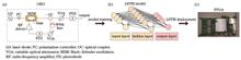
ObjectiveAs the cornerstone of network information transmission, the optical fiber communication network currently carries more than 90% of the global data traffic transmission, and its security is vital to maintaining information transmission privacy. Optical fiber communication is traditionally considered to be relatively secure. However, with the progress of communication technology, such as the application of wavelength division multiplexing and optical amplification technology, despite the greatly improved transmission capacity and distance, concerns about the potential eavesdropping risk of optical fiber communication systems are caused. At present, secure communication technology is mainly divided into two categories of mathematical algorithm encryption and physical layer encryption, with more attention paid to the latter category because of its ability to face high performance computing threats. Meanwhile, quantum key distribution provides absolute security in theory, but faces technical obstacles in implementation, such as low efficiency of single photon detection and large transmission loss, thus limiting its practicability. As a method of physical layer encryption, chaotic secure communication employs the randomness of chaotic optical signals to encrypt information. However, it is a big challenge to realize wide-band chaotic synchronization in high-speed systems, mainly because the initial value sensitivity of chaotic systems makes it difficult to accurately match the parameters of the receiving and sending terminals. To solve the difficulty of chaos synchronization at the receiving and sending ends of traditional chaotic encryption communication systems, some studies have proposed to adopt deep learning technology to realize chaos generation and synchronization, but most of the current studies are only offline processing on computers. Therefore, we propose a method based on deep learning technology to model the optoelectronic oscillation chaotic source to realize the digital domain generation of chaos. Additionally, the chaotic AI model trained by the host computer is deployed on the field programmable gate array (FPGA) and applied to real-time chaotic sequence generation and random number generation.MethodsBased on the long short-term memory (LSTM) network, the optoelectronic oscillation chaotic source is modeled. After pruning optimization, the model is deployed on FPGA to generate chaotic sequences and the random number in real time by a digital-to-analog converter (DAC) chip. Firstly, the chaotic AI model trained by the host computer is optimized and pruned, and the effective network parameters are imported into FPGA and saved. Then the hardware structure of the chaotic AI model is designed on FPGA to generate chaotic sequences. Meanwhile, the chaotic AI model is utilized for real-time random number generation based on the post-processing method optimized by the least significant bit selection. Finally, the chaotic sequence and random number generated by the model are converted into analog signal output by the DAC chip.Results and DiscussionsBased on the chaotic AI model deployed on FPGA, the DAC chip is driven to output chaotic waveform in real time at a sampling frequency of 70 MHz. Compared with the chaotic AI model before optimization, the FPGA’s DSP module resource consumption is reduced by about 31.7%, the Block RAM (BRAM) resource consumption is reduced by 58%, the model calculation delay is reduced by about 44.4% (Table 2), and the model’s prediction accuracy has almost no loss (Fig. 9). By drawing the phase diagram of the original optoelectronic oscillation chaotic source and the chaotic AI model deployed on the FPGA (Fig. 10), it is proved that the deployed model retains the chaotic output characteristics of the original optoelectronic oscillation (OEO) system. By adding a small disturbance of order 10-8 to the excitation signal of the chaotic AI model, the mean square error of the output of the chaotic AI model before and after adding the perturbation is calculated (Fig. 11), which verifies the sensitivity of the model to the initial value and further proves the output chaos of the model. Based on the post-processing method optimized for the least significant bit selection, random numbers are generated at a rate of 70 Mbit/s, and the results can pass the NIST SP 800-22 randomness test (Table 3).ConclusionsTo solve the problem of wide-band chaos synchronization in traditional chaotic encryption communication systems, we model the optoelectronic oscillation chaotic source based on the LSTM network. After optimized pruning, the chaotic AI model is deployed on FPGA, and the DAC chip is driven to output a chaotic sequence in real time at a sampling frequency of 70 MHz. Compared to pre-optimization, the DSP module resource footprint on the FPGA is reduced by about 31.7%, the BRAM resource footprint is reduced by 58%, and the computation latency is reduced by about 44.4%. The chaotic output characteristic of the deployed model maintaining the original OEO system is proved by the phase diagram. The sensitivity of the model to the initial value is verified by calculating the mean square error between the output of the chaotic AI model before and after adding small perturbations. Additionally, based on the least significant bit selection optimization post-processing method, we further apply the deployed chaotic AI model to generate a real-time random number with 70 Mbit/s bit rate, and the obtained results can pass the NIST SP 800-22 test.
Oct. 12, 2024Vol. 44 Issue 19 1906002 (2024)
Guilong Dai, Jiangfei Huangfu, Xiaoyu Wang, and Xingyou Li
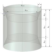
ObjectiveDue to its elusive volumetric effect, the transparent packed-bed solar receiver that comprises quartz glass spheres and ceramic balls is a promising new approach as a reliable and cost-effective high-temperature receiver. However, this solar receiver suffers high reflection loss because the reflectivity of the transparent surface relates to the reflection area and the incidence angle, which limits its thermal efficiency and outlet temperature. To reduce the reflection loss of the transparent packed-bed solar receiver exposed to the incident solar radiation, a modified quartz glass Rasching ring (a hollow short cylinder whose outer diameter is equal to its length) with cut bottom surfaces is proposed and developed. The modified quartz glass Rasching ring can diminish the reflection loss by decreasing the reflection area through cutting bottom surfaces. Four types of mixed-packed solar receivers, including single silicon nitride ceramic ball (PB), quartz glass ball?silicon nitride ceramic ball (BB), quartz glass Rasching ring?silicon carbide ceramic ball (RRB), and quartz glass Rasching ring with cut bottom surfaces?silicon carbide ceramic ball (CRRB) models and prototypes are adopted to investigate the reflection loss of the modified quartz glass Rasching ring.MethodsThe overall reflection loss of four different mixed-packed solar receivers is tested by spectrophotometer and estimated using a weighted average scheme. Then, a 3D ray-tracing model is employed to investigate the reflection loss of the mixed-packed solar receiver based on geometrical optics together with the particle scale model. The incident solar radiation impinging on the inlet aperture of the mixed-packed solar receiver is produced by a parabolic solar concentrator associated with a grid light source in TracePro software. The test results under the parallel light condition have verified the reliability of the numerical model and the corresponding numerical method.Results and DiscussionsResults show that CRRB receiver can significantly reduce the reflection loss of concentrated solar radiation compared to the other three receivers. The reflection loss of CRRB receiver is only 1.9% when the tube-to-particle diameter ratio (D/d) is 5, while that of PB, BB, and RRB receivers is 8.8%, 11.6%, and 16.4% (Fig. 10), respectively. When the layer number of the modified quartz glass Rasching ring is less than 5.0, the reflection loss of CRRB receiver reduces as the layer number increases. However, the reflection loss remains constant when the layer number exceeds 5.0 (Fig. 11). Similarly, when the cut angle of the modified quartz glass Rasching ring is less than 45°, the reflection loss of CRRB reduces as the cut angle decreases. In contrast, the reflection loss remains unchanged once the cut angle exceeds 45° (Fig. 12). The greatest overall benefit would be achieved with 3–5 quartz glass Rasching ring layers with a cutting angle of 20° to 40°.ConclusionsThe modified quartz glass Rasching ring with cut bottom surfaces can significantly reduce the reflection of the packed-bed solar receiver. This modified quartz glass particle can be applied in advanced high-temperature power cycles as it is cost-effective and efficient.
Oct. 12, 2024Vol. 44 Issue 19 1908001 (2024)
Bangyong Sun, Yuhan Shi, and Tao Yu
ObjectiveCamouflage detection aims to distinguish and separate the characteristics of camouflage targets and natural backgrounds from battlefield images, determining the category attributes and coordinate information of the targets. Conventional optical detection struggles with distinguishing “same color and different spectrum” or “foreign object and same spectrum” properties between camouflage targets and backgrounds. As a result, existing camouflage detection primarily relies on spectral imaging or polarization imaging technology. Recently, scholars have combined the advantages of these technologies to develop polarization spectral cameras, which simultaneously capture spectral and polarization information. Image fusion technology further enhances target visibility and contrast between artificial targets and natural backgrounds. Therefore, studying image fusion technology for multimodal data is crucial for improving the accuracy of camouflage target detection under multi-sensor imaging conditions.MethodsWe propose a polarization spectral image fusion method to achieve accurate detection of camouflage targets using the generated fusion images. The process includes four main parts. Firstly, using our team-developed polarization spectral camera, we image backgrounds containing camouflage targets to obtain spectral cubes with four different polarization states. Secondly, we preprocess the polarized spectral images to make them suitable for network input, including spectral reconstruction, polarized image registration, and image denoising. We select single-band images suitable for detection by analyzing the comparative characteristics of camouflage targets and backgrounds in the four polarized spectral cubes. Then, we fuse the four polarized images using PE-Net to enhance polarization semantic information, improving our fusion strategy, and output high contrast fused images of the camouflage targets and backgrounds. Finally, we use the Otsu binary segmentation algorithm to detect camouflage targets and obtain their binary position information.Results and DiscussionsThe proposed polarization spectrum fusion method, Po-NSCT, performs better on four non-reference indicators compared to seven comparison methods (Fig. 9). Compared with NSCT, it increases information entropy (EN) by 0.0656, average gradient (AG) by 2.0912, standard deviation (SD) by 2.3816, and spatial frequency (SF) by 5.8511. Although it decreases in QAB/F compared to NSCT, introducing Stokes vector Q for semantic guidance improves non-reference indicators for better camouflage target detection. For advanced camouflage target detection tasks, Otsu binary segmentation is performed. The Po-NSCT fusion method fully recognizes 12 types of camouflage targets, including nets, suits, and helmets. Compared with the seven comparison methods, the proposed method significantly improves the intersection to IoU, accuracy, and F1 score, with an IoU increase of 0.1543, accuracy increase of 0.1778, and F1 score increase of 0.1068 compared to the original polarized spectral image (Fig. 13). The experimental results show that our proposed fusion method enhances camouflage detection accuracy and reduces the background misjudgment. The polarization semantic guidance module and improved fusion strategy achieve optimal indicators, enriching image information, improving image contrast, and enhancing image texture details. Polarization spectral imaging leverages multiple sensor advantages to enhance image detection performance.ConclusionsThis paper proposes a polarization spectrum image fusion method named Po-NSCT, which utilizes non-downsampling contour wave transformation for recognizing and detecting camouflage targets. The study comprises three main parts. Firstly, we propose the Po-NSCT fusion method to enhance image fusion performance for polarization spectral images. Secondly, we introduce a polarization semantic guidance module to suppress redundant information in polarization spectral images. Finally, we improve target detection accuracy by preprocessing high and low-frequency images before fusion, leveraging the specificity of polarization information. Polarization spectral imaging technology integrates imaging, spectral, and polarization technologies to enhance target recognition in complex environments. Applying this technology for image fusion tasks filters image information and retains more useful information. By fusing spectral and polarization images, effective complementarity of advantageous information from different modalities is achieved, compensating for single sensor limitations and showcasing unique advantages. This method provides a novel image processing approach for polarization spectral imaging systems and holds significant development potential.
Oct. 12, 2024Vol. 44 Issue 19 1910001 (2024)
Yucong Zhou, Chao Ye, Zihan Lin, Chunlian Zhan, and Han Gao
ObjectiveDue to Rayleigh scattering, the distribution pattern of polarized light in the sky varies regularly with the change in the position of the sun. Taking advantage of this distribution, polarized skylight navigation technology can achieve anti-interference and fully autonomous orientation and navigation with no cumulative error, making it widely applied in the areas of aerospace, military operations, and underwater navigation. However, under cloudy weather or complex scenes with obstructions such as trees and buildings, the polarization images of the obstructions do not obey the Rayleigh scattering principle. Therefore, directly using sky polarization images of complex scenes for navigation orientation will reduce navigation accuracy. To solve this issue, various imaging segmentation methods have been proposed for separating sky and occlusion information, but they still have some limitations. For example, the method of using neural networks for obstruction segmentation requires a large amount of data and time for training, making it hard for model application, diagnosis, and repair. Using polarization degree gradient as a threshold to extract effective polarization information often needs to set gradient thresholds manually and requires a large number of experiments, which lacks universality. Therefore, we propose an image segmentation algorithm (SO-Otsu) based on the snake optimization (SO) algorithm and the Otsu method to achieve fast, stable, and self-adaptive polarization navigation of mobile carriers such as drones, cars, and ships under cloudy weather or complex scenes with different obstructions.MethodsBefore applying the SO-Otsu algorithm to segment obstructions and sky in the polarization images for navigation accuracy improvement, the bilinear interpolation algorithm is first used to extract four images with different angles from images captured by a polarization camera. Then Stokes vectors are used to obtain the sky polarization degree image and polarization azimuth image. By using the Otsu algorithm, the maximum inter-class variance of polarization degree images and the optimal segmentation threshold for sky and obstructions identification can be found automatically. At the same time, to speed up the optimal threshold finding procedure, the SO algorithm is applied. A binary mask is designed using the optimal threshold to process the sky polarization azimuth image, remove the polarization information of occlusion, and retain the polarization information of the sky in this image. Finally, utilizing the principles of solar vector, the Rayleigh scattering model, and the polarization information obtained from the SO-Otsu method, the relative azimuth of the sun can be calculated for heading angle calculation. To verify the effectiveness of the SO-Otsu method on polarization image segmentation, two sets of polarization images are captured and analyzed: artificial obstruction with an occlusion rate between 25% and 85% and real environments with an occlusion rate between 17% and 83%. Under each specific occlusion rate, the precision turntable is rotated from 0° to 360° with 10° increments, and the images are taken at each angle. A total of 37 images and data are collected and analyzed. In addition, to evaluate the effect of the SO-Otsu method, the polarization image processing parameters including peak signal-to-noise ratio, optimal threshold, iteration times, and run time using SO-Otsu and Otsu methods are compared.Results and DiscussionsAs shown in Table 1, when segmenting the same image, the SO-Otsu algorithm has better iteration times and algorithm performance than traditional Otsu algorithms, effectively reducing the exhaustive search time by about 40%. The calculated heading angle errors under artificial occlusion are shown in Fig. 8 and Table 2. It can be seen that, when the occlusion rate ranges from 25% to 85%, the maximum error of the heading angle is less than 2.6°. The overall accuracy of the calculated heading angle after segmentation is better than that of without segmentation. Although as the occlusion rate increases, the effective number of pixels used for calculation after segmentation decreases, and the root mean square error gradually increases, it remains within 0.95°. The calculated heading angle errors under occlusion including trees and buildings are shown in Fig. 9 and Table 3. It can be seen that, when the occlusion rate ranges from 17% to 83%, due to the interference of abnormal pixels, the maximum heading angle error calculated without segmentation exceeds 180° while the maximum heading angle error calculated by the SO-Otsu method does not exceed 1.59°. Meanwhile, the accuracy of the calculated heading angle after segmentation is significantly improved, with a root mean square error of less than 0.75°.ConclusionsWe first use a bilinear interpolation algorithm to obtain polarization images from four angles for further polarization information analysis and calculation. By combining SO with the Otsu algorithm, the polarization degree image of sky polarization is directly segmented, and then the abnormal pixel information points in the image are removed. The retained effective pixel information points are combined with the Rayleigh scattering model to calculate the heading angle. The experiment results reveal the time using the SO-Otsu algorithm to segment a polarization degree image is less than 0.005 s, effectively reducing the heading angle calculation time by about 40%. By analyzing the experimental results of multiple sets of different occlusion rates and occlusion conditions, we find that when the occlusion is a baffle with an occlusion rate between 25% and 85%, the root mean square error of the calculated heading angle is less than 0.95°. When the occlusion rate of buildings and trees ranges from 17% to 79%, the root mean square error of the calculated heading angle is less than 0.75°. Compared with directly using images with abnormal pixel information to calculate the heading angle, our method can effectively improve the accuracy of the heading angle. The SO-Otsu image segmentation algorithm provides a new approach for fast and self-adaptive polarization navigation of mobile carriers such as drones, cars, and ships under complex scenes. In the future, to further improve the segmentation effect of polarized images, various algorithms need to be considered and combined to eliminate the influence of high polarization reflected light generated by occluded surfaces, thereby achieving more accurate and stable polarization navigation orientation.
Oct. 12, 2024Vol. 44 Issue 19 1910002 (2024)
Yi Zhang, Quan Yuan, Yifan Wu, Boping He, Qin Ge, Yuhang Yang, Qingyue Zheng, Shujie Yang, Fei Wu, and Shuming Wang
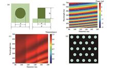
The chosen meta-atom structure utilized TiO2 as the medium due to its widespread availability in the visible-light band, specifically in the range of 400?700 nm, where it exhibits high transmittance. In addition, the optical loss was minimal, and the relevant metasurface fabrication technology has been fully developed. The meta-atom structure was arranged periodically, and the transmission phase was tailored by adjusting the diameter of the meta-atoms according to the phase theory. Subsequently, the metasurface phase was carefully controlled, and phase compensation corresponding to different positions was implemented to achieve the dispersion function of the metasurface. Our design ultimately chose a square shape as the substrate for the unit structure and a cylindrical shape with spatial symmetry for the meta-atoms. During the design process, increasing the height of the meta-atoms augmented the corresponding phase change, albeit at the expense of increased fabrication complexity. To realize a sufficient phase change while simplifying processing, striking a balance between the height of the meta-atoms and the desired phase became crucial. Due to the constraints of current fabrication technology, we opted for a uniform height for all the meta-atoms within the metasurface. Utilizing the finite-difference time-domain (FDTD) simulation method, we designed the geometric parameters of the meta-atoms, allowing us to obtain the transmittances and phases of the elemental structure with varying geometric parameters. Subsequently, we compiled a database incorporating data such as phase and transmittance.A numerical simulation method is utilized to simulate the single channel, as depicted in Fig. 3. Through a ray-tracing software simulation, we project the input image onto the position of the metasurface. To replace the designed metasurface, we opt for a combination of a grating and a mask layer. The spectral system dispersion results in a 12 μm length span across the bandwidth in the range of 400?700 nm. Additionally, we obtain the full spectral images by simulation (Fig. 4). In conclusion, a genetic algorithm is used to determine the light intensity coefficient of each channel to reconstruct the normalized spectrum (Fig. 5). The fitting results demonstrate the practical applicability of the proposed spectral imaging system.During the spectral reconstruction stage, we used a genetic algorithm, optimized over 30 generations, to obtain the normalized spectra. Through inversion on multiple multispectral datasets, all results exhibit perfect alignment with real spectra, achieving a spectral resolution of 30 nm. In summary, the integration of a spectroscopic metasurface into a charge-coupled device camera directly forms a spectral imaging system immune to the polarization state of incident light. This enhancement significantly broadens the applicability of the system. Furthermore, a high spectral resolution can be achieved by introducing different metasurface parameters. While our simulation verification is limited to the visible range, the design principles and methods of this system can be extrapolated to other bands, such as the near-infrared region.ObjectiveTraditional spectral imaging systems rely on bulky optical components to achieve high spectral resolution, which pose challenges for miniaturization and portability. However, as a novel subwavelength artificial optical platform, a metasurface offers multi-degree-of-freedom control over light, including amplitude, phase, polarization, wavelength, and orbital angular momentum. Consequently, metasurfaces have emerged as an impressive advancement in the optical field leading to the development of numerous optical systems based on metasurfaces. These systems have found applications in various optical fields, such as imaging, holography, optical encryption, and quantum information. The planar structure of the metasurface enables systems to be small and light, providing a new solution to issues commonly encountered in traditional spectral imaging systems, such as large size, complex structure, limited functionality, and high cost.MethodsWe utilized TiO2 to design the metasurface structure and successfully implemented a spectroscopic metasurface using the transmission phase principle. Our spectral imaging system comprised 10 channels, each offering a spectral resolution of 30 nm. Alongside the spectroscopic metasurface as the primary component, the system relied on a genetic algorithm to rebuild the spectral intensity.Results and DiscussionsThe fixed meta-atom structure has a height (H) of 1000 nm and a period (p) of 220 nm. By maintaining H and p constants while varying the radius of the unit cell, we obtain corresponding phase distributions and transmittances for different radii. The nanopillar radius ranges from 80 to 180 nm, ensuring comprehensive 2π phase coverage and high transmission (Fig. 2).ConclusionsWe designed a spectroscopic metasurface utilizing the transmission phase principle, employing TiO2 as the material. The working wavelength is selected in the range of 400?700 nm, and a dispersion-type spectral imaging system is established. The FDTD method is utilized to optimize the meta-atom diameter and establish the parameter values along with the corresponding arrangement of the metasurface. Subsequently, 11 spectral channels are selected as outputs within the visible range of 400?700 nm. To validate the performance of the spectral imaging system, we conducted full-image simulations using ray-tracing software.
Oct. 12, 2024Vol. 44 Issue 19 1911001 (2024)
Fan Cao, Bo Zhou, Zhiqiang Liu, and Mao Ye
ObjectiveThe simplest way to achieve high-resolution imaging is by increasing the number of pixels per unit area of the image sensor. However, this can lead to smaller pixel sizes, which in turn increases scattering noise, ultimately degrading image quality and raising costs. Super-resolution (SR) imaging involves acquiring a sequence of images of the same scene with slight displacements and then synthesizing these to create a higher-resolution image. The multi-frame SR reconstruction technique primarily involves: 1) sub-pixel shifted image acquisition of the same scene, 2) alignment of the acquired images, and 3) the use of interpolation methods to obtain higher-resolution images. Conventional methods that involve using double optical wedge rotation and liquid crystal lens optical axis shift suffer from significant image distortion, complex control mechanisms, and slow response speeds. We propose a super-resolution imaging system utilizing a liquid crystal optical wedge device that electronically modulates beam deflection to acquire sub-pixel shifted images. By simply adjusting the amplitude of the applied voltage, the deflection angle and direction of the beam can be precisely controlled without mechanical movement. The liquid crystal optical wedge device can achieve a minimum thickness of just a few micrometers, resulting in fast response times.MethodsIn this study, we propose a super-resolution imaging system that incorporates a liquid crystal optical wedge device paired with a polarizer and a fixed focal length camera module. We first introduce the principle of electronically modulated beam deflection within the liquid crystal optical wedge and theoretically analyze the relationship between beam deflection and image displacement. A sequence of images of the same scene is captured at varying driving voltages, and the average displacement between images is measured using the Keren alignment method. Experimental results demonstrate that electronically modulated sub-pixel image shifts are achieved within acceptable error margins. The limiting resolution and modulation transfer function (MTF) of the images are evaluated using HYRes and Imatest software, respectively, to quantify improvements in image resolution and contrast.Results and DiscussionsThe initial image of the ISO12233 resolution chart is shown in Fig. 9. Using HYRes software, we measure the TV lines in both vertical and horizontal directions to determine the limiting resolution for the initial image, a single-frame interpolated image, and the multi-frame super-resolution image, as shown in Table 2 and Fig. 11. The comparison shows that the resolution of the synthesized multi-frame super-resolution image is improved by 55.0% and 58.8% in the vertical and horizontal directions, respectively, compared to the initial image, and by 24.6% and 37.2% compared to the single-frame interpolated image. The modulation transfer function curve, obtained using Imatest software to measure a black-and-white diagonal pattern with a specific tilt angle, is shown in Fig. 12. The curve indicates that the multi-frame super-resolution image effectively enhances image contrast in high-frequency regions due to the introduction of additional information.ConclusionsWe report on an optical system designed for super-resolution imaging using a liquid crystal optical wedge device capable of electrically modifiable beam deflection. The device’s electrode structure and beam deflection principle are discussed, and the theoretical relationship between image displacement and applied voltage is analyzed. Experimental results show that the device can accurately achieve image sub-pixel image displacement without mechanical movement. The liquid crystal optical wedge device used in this study features a 2 mm×2 mm square aperture in its working area and a device box thickness of 5 μm. By shifting the beam deflection direction three times, a sequence of four images with defined displacement is captured, enabling multi-frame super-resolution imaging. HYRes software is used to measure the limiting resolution of the multi-frame super-resolution image, the initial image, and the bicubic linear interpolated image. The comparison shows a significant enhancement of approximately 55.0% relative to the initial image. Compared with other methods for acquiring multi-frame images, the device used in this study offers advantages such as no mechanical movement, a simple driving method, fast response time, and no effect on the optical focus of the system, making it a viable solution for achieving high-resolution imaging in large-scale systems.
Oct. 11, 2024Vol. 44 Issue 19 1911002 (2024)
Xianmeng Shen, Renjin Shao, Suodong Ma, Donglin Pu, Chinhua Wang, Junxue Wang, Yue Ben, and Chufeng Xue
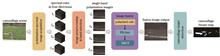
ObjectiveSpectral imaging is a multidimensional information acquisition technology that combines traditional imaging with spectral analysis. Traditional spectral imaging technologies are often complex and costly, making them difficult to popularize in dynamic or transient scenes. In contrast, snapshot spectral imaging technology can capture spatial and spectral data within a single integration cycle of the imaging system. With the development of micro-nano optics, diffractive optical elements (DOEs) have been applied to snapshot spectral imaging due to their small size and high design flexibility, further reducing device volume and hardware costs. However, existing snapshot spectral imaging technologies based on DOEs are susceptible to the effects of diffractive lens fabrication accuracy and various errors during imaging. Moreover, they require sophisticated spectral image reconstruction algorithms, limiting their widespread application under practical conditions. To fully utilize the advantages of diffraction lens, we conduct in-depth research on their imaging and designing principles, error analysis, image acquisition, reconstruction, and deep learning algorithms. A new type of snapshot differentiable coded spectral imaging system is proposed, which can optimize the design of optical systems and achieve high-quality reconstruction of spectral images. The system demonstrates promising results in simulation and practical image restoration, showcasing its practical value.MethodsWe introduce a novel approach using a hybrid diffractive-refractive lens scheme, which effectively reduces the microstructure density of DOEs (Fig. 1). This not only shortens the system focal length and decreases DOE fabrication complexity but also enhances the imaging signal-to-noise ratio. Furthermore, it employs a deep unfolding framework alongside an improved Transformer model (DUF-DST, Fig. 2) to facilitate the reconstruction of diffraction spectral images. Building upon this framework, we conduct a comprehensive analysis of error sources in snapshot diffraction spectral imaging systems. This includes fabrication errors during DOE preparation (Figs. 3 to 4), component assembly discrepancies during imaging (Figs. 5 to 6), as well as sensor and environmental noise factors (Fig. 7). Through rigorous quantitative validation experiments, we quantify the magnitude of each error and assess their impact on imaging and final reconstruction outcomes via meticulous modeling and simulation. Finally, throughout the DOE design and reconstruction model training phases, we employ a joint optimization method to effectively mitigate these error sources.Results and DiscussionsTo validate the effectiveness of the aforementioned optical model and spectral image reconstruction method, we conduct simulation tests by establishing a comprehensive image degradation model and reconstruction network framework based on actual experimental parameters. The DOE utilized in this paper is devised using an end-to-end joint optimization method (Fig. 8), which takes partial machining errors into consideration during the design optimization process. Through degradation-reconstruction testing on 30 scenes, the reconstructed results achieve an average peak signal-to-noise ratio (PSNR) of 37.16, a structural similarity index (SSIM) of 0.9881, and a spectral angle mapper (SAM) of 0.0591 (Fig. 9). Comparison with results from four other mainstream image reconstruction models demonstrates that the DUF-DST model employed here exhibits superior reconstruction performance (Fig. 10). Furthermore, to verify the effectiveness of the error suppression method proposed in this paper, a series of indoor and outdoor experiments are conducted (Figs. 12 to 18). These experimental scenarios closely resemble real-world application environments and encompass various analyzed errors and noise. Reconstruction of the original images captured is performed using a reconstruction network optimized based on error considerations. Experimental results indicate that the reconstruction model employed in this paper achieves high-quality restoration of spectral images, and the proposed error suppression method significantly enhances the robustness of the reconstruction algorithm to errors and noise in actual imaging processes.ConclusionsAddressing the inadequate consideration of errors in the imaging process by current diffractive spectral imaging technology, which leads to limited imaging effects, we introduce a snapshot diffractive spectral imaging system along with a hybrid error suppression method. It systematically examines errors (height map error and graphic structure location error) arising from diffraction lens fabrication and component assembly, as well as system and environmental noise. Based on these error terms, a diffraction degradation model is constructed, and a deep unfolding network is used to reconstruct the diffraction-blurred images. By jointly training the degradation model and reconstruction network, the reconstruction algorithm’s generalization ability to errors and noise is significantly enhanced. Relevant simulations and indoor/outdoor experiments demonstrate that the imaging model, with error suppression and the proposed reconstruction algorithm, effectively enhances the imaging quality of the system in practical application scenarios, achieving high-quality reconstruction of spectral images within a single integration cycle.
Oct. 12, 2024Vol. 44 Issue 19 1911003 (2024)
Zhixiang Li, Quanying Wu, Junliu Fan, Baohua Chen, and Xiyu Liu
ObjectiveA sparse aperture refers to a configuration where multiple sub-mirrors are arranged in a non-redundant pattern, utilizing interference techniques. This results in a system with a smaller light-receiving area than a single large aperture, while still capturing comparable information. The polarization-induced aberrations in each optical element of a sparse aperture optical system significantly influence the overall imaging performance. However, limited research has been conducted on the polarization characteristics of such systems. We systematically examine the polarization aberrations of sparse aperture imaging systems using the polarization ray tracing theory.MethodsIn this study, we use the Golay3 sparse aperture imaging system, designed with ZEMAX optical software, as a case study. Based on polarization ray tracing theory, we calculate the polarization aberrations of the system, including diattenuation and phase retardation. The system’s Jones pupil is derived, and through Fourier transformation, we calculate the system’s amplitude response matrix (ARM) and modulation transfer matrix (MTM).Results and DiscussionsOur theoretical model reveals that, at a zero field of view (FOV), the diattenuation and phase retardation of the sparse aperture optical system exhibit rotational symmetry. The maximum values of the system’s diattenuation and phase retardation are 2.313×10⁻³ and 2.315×10⁻² rad, respectively, as shown in Fig. 6 and Fig. 7 indicate that across the full FOV, the Peak-to-Valley (PV) values of diattenuation and phase retardation share a consistent distribution characteristic, exhibiting symmetrical distribution along the Y-field. By performing a Fourier transformation on the Jones pupil, we obtain the system’s ARM, as shown in Fig. 10. The diagonal matrices MARM,XX and MARM,YY of ARM are close to the amplitude response function of a diffraction-limited system. Figs. 10(b) and (c) illustrate that the non-diagonal matrices MARM,XY and MARM,YX have equal magnitudes, exhibiting a symmetrical structure not centered at the origin but symmetric around a horizontal line with four peak points. We calculate the MTM of the sparse aperture optical system under different filling factors. Fig. 12(a) demonstrates that the matrices in the horizontal direction of MTM are symmetrically distributed about the diagonal. From the MTF of the main diagonal, it is evident that a higher filling factor results in higher MTF values at the same spatial frequency, with consistent trends in the MTF curves. The maximum MTF positions of the non-diagonal MTFs are not at zero frequency. M01, M02, M23, and M03 show that as the filling factor decreases, the peak value of the MTF curve lowers, and the cutoff frequency shifts to lower frequencies. Fig. 12(b) indicates that the MTF values on the diagonal decrease as the filling factor decreases. On the non-diagonal lines of MTM, the maximum MTF values are at non-zero frequencies, exhibiting the same distribution trend across different filling factors, with the maximum values increasing as the filling factor decreases. The MTF curves show significant variations at mid-to-high frequencies.ConclusionsOur study uses polarization ray tracing methods to calculate the polarization aberrations of the Golay3 sparse aperture optical system. The results indicate that under a 0° FOV condition, the system’s diattenuation and phase retardation are primarily caused by the sub-mirrors. Polarization aberrations are closely linked to the structural characteristics of sparse aperture optical systems. All mirrors in the Golay3 system are rotationally symmetric around the optical axis, leading to rotational symmetry in diattenuation and phase retardation. Across the full FOV, the PV values are symmetrically distributed along the Y-field, increasing with the Y-field and decreasing towards -0.1° along the X-field. Polarization crosstalk in the Jones pupil and ARM exhibits horizontal symmetrical distribution, with four peak points in the latter. As the filling factor increases, the non-diagonal matrices of the MTM decrease in the horizontal direction’s MTF, while the vertical direction’s MTF increases. Polarization aberrations of sparse apertures are closely related to the arrangement of sub-aperture arrays, and their presence can reduce system imaging quality.
Oct. 10, 2024Vol. 44 Issue 19 1911004 (2024)
Yuchen Wei, Jiechun Weng, Penglong Wang, Bing Chen, Zeren Gao, and Yu Fu
ObjectiveThe increasing complexity of mechanical structures and equipment, driven by industrial technology advancements, necessitates prompt damage repairs. Failure to address issues such as internal or surface cracks not only compromises structural integrity but also poses safety risks to operators. Identifying the precise location of structural damage has become an urgent issue. Vibration measurement techniques primarily include contact and non-contact methods. The contact measurement method involves attaching strain gauges or installing accelerometer sensors on the object’s surface to evaluate vibration response, which can alter the structure’s dynamic characteristics and limit data collection points. In contrast, the non-contact method provides high spatial resolution and accuracy but comes with a complex optical setup and limited environmental interference resistance. With image processing technology’s rapid progression, digital image correlation (DIC) has emerged as an effective non-contact measurement tool. Our study explores using DIC for structural dynamic response measurement and damage detection by comparing changes in modal parameters (frequency, damping, and modal shapes) between damaged and undamaged structures. Notably, modal shapes are sensitive indicators of local damage, closely related to its stiffness distribution. Once the structure is damaged, the stiffness in the damaged area changes, leading to abnormal changes in the displacement mode. However, traditional damage detection methods based on structural modal shape analysis face certain limitations: 1) The spatial resolution of damage structure measurement depends largely on the spatial sampling rate of the measurement method. 2) Damage identification methods rely on comparing the vibration response of the damaged structure with that of an undamaged structure. However, obtaining baseline data from undamaged structures is often challenging. 3) Measurement data contains random noise, which not only makes signal processing complex but also significantly affects the accuracy of damage identification. We introduce a DIC full-field vibration measurement method that utilizes modal shapes to identify damage locations. We propose frequency domain noise decoupling technology that utilizes laser Doppler vibrometer (LDV) single-point data to assist the displacement field of DIC.MethodsDIC is a non-contact optical measurement method that utilizes cameras to capture the patterns of the measured object at different times and derives displacement fields by matching image feature points. In this study, we employ DIC to measure the operating deflection shape (ODS) of the structure under natural frequency excitation to identify damaged regions. When the excitation signal of the structure is at its natural frequency, the vibration response of the structure is primarily dominated by that mode, making the ODS closely resemble the structural modal shape. However, DIC experiments are susceptible to systematic and random errors, leading to measurement data where displacement fields are mixed with random noise, complicating damage detection using DIC measurements. To address this, we propose a noise decoupling technology using a bandpass filter in the frequency domain to eliminate non-vibrational frequency components from the DIC results. Furthermore, LDV is utilized to accurately measure the vibration response, guiding the noise decoupling process for DIC data. By separating vibration signals from noise in the frequency domain, we enhance the signal-to-noise ratio of the modal shapes. Subsequently, Chebyshev polynomial fitting is used to remove high-frequency information from the displacement field, reconstructing the baseline data of the undamaged structure. The residual analysis method then locates abnormalities by calculating differences between modal shapes and fitted baseline data. In structures with uniform material distribution, peaks in residuals indicate damage locations. This approach takes full advantage of the high spatial sampling rate of image measurements for precise damage localization. The schematic diagram of the DIC measuring vibration modes to detect structural damage is presented in Fig. 6.Results and DiscussionsExperiments are conducted on cantilever plates I and II to validate the efficacy of the proposed method. Firstly, we measure the natural frequency of the cantilever plates I and II with LDV. Then, DIC captures the modal shapes of the structure under excitation by the first four natural frequencies. The operational deflection shape of cantilever plate I is then processed with a bandpass filter to confirm the effectiveness of the LDV-guided DIC data noise decoupling technology (Fig. 7). The Modal Assurance Criterion is used to compare Ansys simulation data with the DIC measurement results post bandpass filtering to verify the effectiveness of the proposed filtering method (Fig. 8). Afterwards, the modal shapes derived after noise reduction are employed to detect structural damage locations. To ensure accuracy in fitting and to avoid overfitting, a seventh-order Chebyshev polynomial is used to establish the baseline data. The structural damage locations on cantilever plates I and II are ascertained by measuring the modal shape obtained under excitation at the fourth and eighth natural frequencies, respectively. Experimental results demonstrate that the modal shapes, once noise-decoupled, could pinpoint the damage locations on cantilever plates I and II with precision. In contrast, the modal shapes that were not filtered failed to reveal the damage locations (Figs. 10 and 11).ConclusionsWe present a damage detection method that leverages DIC for measuring modal shapes. The technique capitalizes on the high spatial resolution of DIC to identify damaged areas within structures. By employing Chebyshev polynomial fitting, this method reconstructs baseline data, eliminating the need for prior baseline measurements. Additionally, frequency domain noise decoupling technology is utilized to remove random noise from the modal shapes, effectively reducing the influence of noise on damage detection. Experimental tests on cantilever plane damage detection confirm the efficacy of the proposed method in detecting structural defects.
Oct. 12, 2024Vol. 44 Issue 19 1912001 (2024)
Zixu Dai, Guohui Yang, Yiheng Gao, Zhilong Su, and Dongsheng Zhang
ObjectiveAs various structures rapidly develop in the engineering field, the measurement of large displacement structures has become an important research topic. Traditional measurement methods cannot meet the practical needs of multipoint or full-field measurements. The binocular stereo vision system has been widely applied in engineering as a contactless displacement measurement tool due to its advantages of simple optical path, full-field non-contact measurement, and large measurement field of view. However, existing binocular stereo vision measurement technologies typically require the binocular cameras to remain fixed after pre-calibration to maintain the stability of the reference coordinate system and the relative pose of the cameras, which ensures the effectiveness and correctness of 3D displacement calculation. This limitation also restricts the measurement range of the system to a certain extent and may cause measurement failures if the area of interest moves out of the field of view due to large deformations. Therefore, the development of a system with tracking measurement capabilities has become an urgent need to balance measurement range and accuracy. We aim to develop a novel technique that can continue measurement in such scenarios.MethodsWe propose a large displacement measurement method based on panning binocular stereo vision, which utilizes imaging units mounted on separate dual-axis panning stages to form a panning vision system. The intrinsic parameters of the imaging units are predetermined through calibration using a chessboard pattern. During large displacement measurements, external parameters are calibrated using coded markers based on the epipolar constraint relationship, followed by an inverse depth bundle adjustment. During measurement, the panning binocular stereo vision system adjusts as the target moves out of the predefined field of view. The external parameters are calibrated using the aforementioned method, and the current coordinates are transformed back to the original using the iterative closest point algorithm. By supplementing corner points or encoded points in the overlapping areas of the field of view before and after panning, a rigid body transformation matrix for the left camera is constructed based on spatial coordinates before and after panning, which ensures alignment with the global coordinate system. Finally, displacement information for the measurement point is calculated during the entire motion.Results and DiscussionsThree experiments are presented in this study. Firstly, we conduct the proposed camera calibration method, showing that the measured displacement value closely matches the real displacement (Fig. 6). With a reference 3 m horizontal field of view, the relative errors in the in-plane and off-plane directions are 0.040 and 0.047 mm/m, respectively. Secondly, we evaluate the accuracy of coordinate transformation based on ICP, with experimental results indicating a relative error of 0.11 mm/m for the coordinate transformation. Finally, we apply the developed panning binocular stereo visual system to measure large displacements. We use a one-dimensional displacement stage to simulate target movement beyond the field of view, which enables continuous displacement measurement. With a single panning operation, the field of view expands from 3 m by 3 m to 5.5 m by 3 m, and the relative errors in predefined translational displacement are less than 0.3% (Fig. 10).ConclusionsA measurement method based on panning binocular stereo vision has been proposed to facilitate measurements when the target moves out of the field of view. This method combines fast camera calibration with key technologies in coordinate transformation. The binocular imaging system adjusts flexibly based on the positional information of the target point within the field of view, effectively preventing measurement failures due to target loss during large displacements. To optimize the acquisition of reliable external parameters, a refined strategy is introduced for camera calibration and coordinate transformation, which integrates optical coding markers and inverse depth bundle adjustment. For fixed feature points within the field of view before and after panning, the ICP algorithm is used to establish the coordinate transformation relationship and complete the entire motion measurement of the target point. This developed system expands the applications of existing binocular stereo vision with accurate displacement measurements, thereby offering a practical and effective solution for measuring large displacements in engineering structures.
Oct. 11, 2024Vol. 44 Issue 19 1912002 (2024)
Yuning Wang, Hanmu Wang, Yicong Feng, Jian Zhou, and Xiaoming Nie
ObjectiveSelf-mixing interference (SMI) is a novel optical measurement technique that utilizes the light reflected back into the laser cavity. Due to the interaction between the feedback light and the medium in the cavity, SMI has high sensitivity. It can obtain high quality signals for targets with rough surfaces without the need for additional target mirrors. SMI also features high resolution, low cost, and compactness, making it widely used in sensing applications. The effective signal of SMI is related to the phase of the laser, so phase demodulation is particularly important. Recently, researchers have used electro-optic crystals and mixers for orthogonal phase demodulation, which can eliminate baseline noise, simplify the algorithm, and increase the measurement speed. However, this method requires the orthogonal signal of the electro-optic modulation signal. Due to the high-frequency nature of electro-optic signals, it is difficult to construct the orthogonal signal. This method does not consider the influence of the initial phase on the harmonic amplitude, while the variation of the harmonic amplitudes can lead to a decrease in accuracy. To address the challenge of constructing orthogonal signals and to solve the problem of random fluctuations in harmonic amplitudes, we propose a new signal processing method based on the Hilbert transform, which can simultaneously simplify the system and improve measurement accuracy.MethodsFirst, the basic SMI model and the fundamental principle of electro-optic modulation are introduced. Subsequently, based on the principle of heterodyning, the reason for the inconsistency in the amplitudes of the two harmonics is discussed, and the influence of this inconsistency on the measurement variance is analyzed by numerical simulation. Then, a self-mixing interference electro-optic modulation device is constructed using a 532 nm solid-state laser, a 251 kHz resonant electro-optic phase modulator, and a photodetector. The laser beam is irradiated onto an aluminum reflector mounted on a piezoelectric transducer (PZT), causing the reflector to make sinusoidal vibrations at a frequency of 5 Hz and a peak-to-peak value of 4 μm. Comparisons are made among three scenarios: no normalization, normalization with fixed coefficients, and normalization using the Hilbert transform. The peak-to-peak interval is gradually increased from 1 to 10 μm, and seven datasets are randomly collected to test the improvement of Hilbert normalization on measurement accuracy. Finally, the applicability of this method is tested when the reflector is subjected to triangular and square wave vibrations.Results and DiscussionsBased on the principle of heterodyning, the random fluctuation of the difference between the initial phase of heterodyning and the initial phase of electro-optic modulation will cause fluctuations in the amplitudes of the two harmonics (Fig. 3), and the inconsistency of the harmonic amplitudes will increase the standard deviation of the measurement (Fig. 4). Measurements are made on a sinusoidal vibration with a frequency of 5 Hz and a peak-to-peak value of 4 μm. A comparison is made between the fixed coefficient normalization and Hilbert transform normalization (Fig. 8). Using the fixed coefficient normalization, the difference in amplitudes between the two harmonics is reduced. However, due to the fluctuations in the harmonic amplitudes caused by laser power fluctuations and feedback light speckle effects with time, it is not possible to find a fixed coefficient that could normalize all harmonic amplitudes over all time periods. With Hilbert normalization, the amplitudes of the harmonics are normalized within each time period, completely eliminating inconsistencies in the harmonics. It also eliminates the random fluctuations in amplitude over time. As a result, without normalization, the standard deviation is 18.2 nm. After normalization with fixed parameters, the standard deviation is reduced to 15.0 nm, and after Hilbert normalization, it is further reduced to 12.5 nm. The measurement accuracy is the highest after Hilbert normalization, indicating that using the Hilbert transform for normalization has certain advantages. The effect of Hilbert normalization under different amplitude conditions obtained in tests shows a significant reduction in the standard deviation after Hilbert normalization (Fig. 10), with a 30% reduction compared to non-normalized data. In addition, this method shows good applicability to both square waves and triangular waves (Fig. 11).ConclusionsIn this study, we analyze the cause of the inconsistency in harmonic amplitudes and propose a normalization method based on the Hilbert transform to solve the problem of harmonic asymmetry and improve the measurement accuracy of the SMI system. The SMI signal modulated by the electro-optic modulator (EOM) is directly heterodyned with the first-order and second-order electro-optic modulation signals to extract the first- and second-order harmonics. Then, the extracted harmonics are subjected to Hilbert normalization to eliminate the asymmetry in harmonic amplitudes caused by the randomness of the initial phase. This method effectively improves the measurement accuracy by reducing the standard deviation by 30%. Measurements of sinusoidal vibrations with amplitudes ranging from 1 to 10 μm peak-to-peak values achieve a measurement accuracy of λ/42 after normalization. In addition, this method can also reconstruct non-sinusoidal waveforms such as square waves and triangular waves, demonstrating strong applicability. The proposed method features high measurement accuracy, simple algorithms, low sampling rate requirements, and strong applicability, providing valuable exploration for high-precision online displacement measurement.
Oct. 12, 2024Vol. 44 Issue 19 1912003 (2024)
Xiaoqing Feng, Su Zhang, Juntong Zhan, Qiang Fu, Jin Duan, Yingchao Li, and Shetian Lu
ObjectiveIn complex environments, unpolarized sunlight undergoes absorption and scattering by atmospheric molecules and fog particles, leading to polarization phenomena that form stable skylight polarization patterns. These patterns change with variations in atmospheric conditions, time, and other factors. The composition, particle size, and properties of aerosols vary significantly over time and across space, making it difficult to quantify their influence on skylight polarization distribution. To accurately simulate the radiative transfer of sunlight through aerosol media, it is essential to consider the aerosols' physical and optical characteristics, as well as their environmental context. Sea fog and land fog differ in their physical and optical properties, which in turn affect the formation of polarization distributions in the sky. However, there has been limited quantitative comparison between theoretical models and field measurements in existing studies. Building on previous research, we simulate the vertical transmission of aerosols by layering the atmospheric medium based on particle size and using the adding-doubling method to solve atmospheric radiation transmission problems. A simulation model for the skylight polarization distribution is developed for both sea and land aerosols. In addition, we design and implement an all-weather, full-period polarization acquisition system to conduct actual measurements and verify the model in both sea and land environments. By quantifying the difference in polarization distribution between sea fog and land fog, we hope to enhance our understanding of sky polarization patterns under different aerosol conditions. It also provides a reference for applying skylight polarization characteristics in polarimetric navigation across sea and land environments.MethodsWe use the adding-doubling method to build simulation models for skylight polarization distribution based on the vector radiative transfer equation, applicable to both sea fog and land fog environments. We also develop an all-weather, full-time polarization acquisition system for practical measurements and validation. The study explores the effects of different times of day and aerosol optical depth (AOD) on polarization distribution, comparing the polarization distributions of different fog types under the same weather conditions. A simulation model solves the radiation transfer equation using the adding-doubling method to obtain the degree of polarization (DOP) and angle of polarization (AOP), showing the particle distribution characteristics of both sea fog and land fog. To verify the model’s accuracy, we construct a field experiment setup that captures the actual polarization distribution. We then analyze the simulation and experimental results of sea fog under different conditions and investigate the effects of fog types on the full-sky DOP distributions.Results and DiscussionsThe DOP values across the entire sky decrease as the solar altitude increases, with the smallest values near the sun and larger values farther from it. The AOP distribution shows symmetry around the meridian line (Fig. 6). Simulations and measurements in both sea fog and land fog environments reveal that increasing AOD attenuates DOP; the higher the AOD, the stronger the attenuation (Figs. 9 and 12). The maximum DOP in sea fog is higher compared to land fog (Fig. 15). The consistency between the simulation and experimental DOP distributions in both environments, calculated using the Pearson product-moment correlation coefficient (PPMCC) and root mean square error (RMSE), exceeds 70% (Table 6).ConclusionsMost research on skylight polarization distribution under different aerosol types remains theoretical, but real foggy environments are dynamic, requiring further field testing to quantitatively assess the differences between theoretical models and practical conditions. We address this challenge by simulating and experimentally studying the effects of different times, AOD levels, and fog types on skylight polarization distribution. The simulation ensures accuracy by solving the vector radiative transfer equation using the adding-doubling method, while the tests employ a fisheye lens and a DoFP polarization camera for rapid image acquisition. The results demonstrate that: 1) the distribution of skylight DOP is more pronounced when the solar elevation angle is low, with smaller DOP values near the sun, and the AOP meridian line shifts counterclockwise over time; 2) as AOD increases, the maximum DOP decreases for both sea and land fog, with sea fog consistently exhibiting higher DOP values; 3) the correlation between simulation and test results, as measured by PPMCC and RMSE, shows good agreement, with a minimum PPMCC of 71.25% and a maximum RMSE of 26.81%. We provide a valuable reference for understanding the influence of different fog environments on sky polarization patterns and their application in polarimetric navigation across both sea and land environments. Further research will focus on minimizing the influence of solar exposure on these measurements.
Oct. 12, 2024Vol. 44 Issue 19 1912004 (2024)
Lijie Zhang, Yanjing Fan, Jingjing Hu, Yuxuan Cheng, and Yiying Gu
ObjectiveIntegrated photonics has undergone significant development in the past two decades, particularly silicon photonics, thanks to the mature complementary metal oxide semiconductor (CMOS) process flow. Despite advancements in silicon photonic chip technology and their widespread applications in various sectors such as lidar, medical detection, and military defense, a significant hurdle remains in the efficient transfer of information between these chips and the external world via optical fibers. Since current manufacturing processes are unable to provide the best properties in a single-material optical system, achieving low-loss transmission between different material systems becomes extremely important. Edge coupling emerges as one of the most promising methods for information exchange in optical chips compared with grating coupling, which exhibits lower coupling efficiency in high-power systems. According to the refractive index of the materials used, edge couplers can be categorized into two types: 1) waveguides with low refractive index and large cross-section size, mainly involving SiOx and SU-8 glue; 2) waveguides with high refractive index and small cross-section size, with representative materials such as SiON and Si3N4. With the development of alignment accuracy in stepper exposure during the optical chip manufacturing process, the manufacturing requirements of multilayer waveguides are gradually being met. Consequently, more research is focusing on waveguides with high refractive index and small cross-section size. However, most proposed edge couplers are based on waveguides of three layers or are based on doping or deep etching of the cladding SiO2. To simplify the manufacturing process while maintaining high coupling efficiency, we propose and optimize a novel edge coupler based on a cross-type heterogeneous multi-core waveguide. By guiding light with silicon nitride waveguide and silicon waveguide together, this design utilizes one less layer of Si3N4 waveguide and eliminates the need for deep etching of SiO2 and the use of SiON.MethodsThe research methodology involves a comprehensive design and simulation process using the MODE Solutions module. The proposed edge coupler is based on a cross-type heterogeneous multi-core waveguide structure (Fig. 1). This structure integrates silicon nitride and half-etched silicon waveguides to achieve high mode field matching between optical fibers and silicon strip waveguides. The structural parameters to be optimized include the width and spacing of the Si3N4 waveguides denoted as w and d, as well as the width and spacing of the half-etched Si waveguides denoted as wSiand dSi. To simplify the optimization process, we divided it into two steps. First, we optimize the w and d parameters using cross-type Si3N4 waveguides, with all five waveguides having the same dimensional parameters. The overlap integral is utilized to measure the mode field matching efficiency, as shown in Fig. 2. In the subsequent optimization step, one Si3N4 waveguide at the bottom was replaced by a half-etched Si waveguide, while the w and d parameters are set to the optimized values obtained in the first step. The simulation results of this step are presented in Fig. 3. Inspired by the research work of Maegami, we employ his method of analyzing the coupling sections of the adiabatic taper to design our adiabatic coupler. This involves calculating and comparing the effective refractive index of the single waveguide and the combination of the two waveguides. Based on these calculations, we divide the adiabatic taper into lower coupling and higher coupling sections. In each section, we optimize the length of the taper, respectively.Results and DiscussionsThe simulation analysis of the proposed edge coupler, conducted using advanced simulation tools, reveals exceptional optical coupling performance. At the wavelength of 1550 nm, the device demonstrated a high mode field matching efficiency, which is crucial for efficiently transferring light between the silicon photonic chip and the high numerical aperture fiber (HNAF). The simulation results indicate a coupling efficiency of 97.1% for the TE mode and 97.5% for the TM mode, highlighting the effectiveness of the design in minimizing optical loss during the coupling process (Fig. 6). The bandwidth capability of the coupler was also evaluated, showing that the design supports a bandwidth of 350 nm while maintaining a polarization-dependent loss (PDL) within ±1%. Additionally, the coupler exhibits an acceptable 1 dB alignment tolerance, allowing for approximately ±1.01 μm displacements for both TE and TM modes (Fig. 8). The simulation results further demonstrate that the proposed edge coupler has a high process tolerance for SiO2 thickness error and horizontal distance error of the silicon nitride waveguides. This resilience to manufacturing imperfections underscores the design’s industrial applicability and potential for reliable, large-scale production. In conclusion, the performance analysis confirms the proposed edge coupler as a promising solution for high-efficiency silicon photonics integration.ConclusionsWith the increasing adoption of Si3N4 waveguides alongside SOI waveguides, we introduce a high-coupling-efficiency cross-type heterogeneous multi-core waveguide edge coupler that avoids the need for deep etching or doping of the SiO2 cladding. The manufacturing process for this structure is relatively straightforward, involving the addition of two layers of Si3N4 waveguides to the traditional SOI chip manufacturing process. Apart from the interlayer distance of the two Si3N4 waveguides, which may not be suitable for multi-project wafer (MPW) fabrication, the remaining processes are compatible with MPW production. Simulation results reveal that the designed edge coupler achieves a coupling efficiency of 97.1% (TE mode at 1550 nm, coupling loss of 0.13 dB) and 97.5% (TM mode at 1550 nm, coupling loss of 0.11 dB) when coupled with high numerical aperture fibers. These fibers can be linked to standard single-mode fibers through thermally expanded core (TEC) technology, resulting in a coupling loss of less than 0.10 dB. Therefore, the total coupling loss is estimated to be less than 0.23 dB (TE mode) and 0.21 dB (TM mode). Additionally, the designed edge coupler exhibits good manufacturing tolerances for waveguide thickness, width, and SiO2 cladding thickness, indicating promising prospects for industrial applications.
Oct. 12, 2024Vol. 44 Issue 19 1913001 (2024)
Shuanghao Jin, Pingwei Lin, Ning Ru, Yanning Ma, Wensong Jiang, and Zai Luo
ObjectiveThe cesium atomic fountain clock is a device that can provide high-precision time and frequency signals by reproducing the SI unit of the second. It is employed in various fields such as quantum precision measurement, satellite positioning and navigation, and geological exploration. With advancements in laser technology and changing application scenarios, the development of cesium atomic fountain clocks has increasingly emphasized compactness, automation, and high reliability. The laser system, being the core component of the cesium atomic fountain clock, traditionally occupies significant space due to spatial light paths and optic components. Larger systems are more susceptible to environmental influences. Therefore, developing compact and highly reliable laser systems is crucial for small cesium atomic fountain clocks.MethodsThe proposed laser system is composed of three main modules: laser frequency stabilization, laser amplification, and laser beam splitting. In the frequency stabilization and amplification modules, a folded double-sided optical path design is employed to control the volume within 210 mm×210 mm×165 mm. The traditional double-pass acousto-optic modulator (AOM) solution is replaced by an open-loop frequency shifting method, eliminating the need for the AOM and associated components. Moreover, in the laser beam splitting module, an electro-optical modulator with a fiber interface is used for 9 GHz modulation, utilizing the edge frequency light generated by phase modulation as repumping light. This eliminates the need for separate repumping lasers and their complex frequency stabilization paths. These improvements significantly simplify the optical path design. Furthermore, the laser beam splitting adopts an all-fiber beam splitting scheme, further compressing the system’s volume.Results and DiscussionsThe frequency of the distributed feedback (DFB) laser remains locked within 50 ms, with the voltage error signal fluctuating within the ±1 V range without any jumps. The central slope of the frequency identification curve is 0.6 V/MHz, and the laser frequency locking range is 3.3 MHz. Upon opening the closed loop at 50 ms, the control voltage of the laser gradually increases, achieving frequency detuning by altering the laser injection current. This results in a 150 MHz frequency shift lasting 2 ms. The laser system begins to return to the initial control voltage at 52 ms, and by 55 ms, the frequency locking state is restored. These results indicate that the open-loop frequency shifting method can achieve rapid and large-scale detuning, meeting the requirements for atomic polarization gradient cooling in small cesium atomic fountain clocks. The laser system demonstrates reliable re-locking capability (Fig. 9). A small cesium atomic fountain clock is operated continuously for 24 h, with cold polarization gradient cooling (open-loop frequency shifting) occurring 43200 times, maintaining atomic number signal fluctuation within 10%. These findings confirm that the open-loop frequency shifting method is repeatable and effective (Fig. 10), replacing the double-pass AOM method.ConclusionsThe compact laser system proposed in this paper utilizes DAVLL technology for frequency stabilization, the open-loop frequency shifting method for rapid and wide-range frequency detuning, and a 9 GHz frequency-stabilized laser for generating repumping light. Compared to existing fountain clock laser systems, this design offers higher miniaturization and reliability. Verified through laser frequency stabilization and frequency shifting experiments, this compact laser system meets the operational requirements of a small cesium atomic fountain clock. In addition, the system can be readily applied to other small cold atom quantum precision measurement instruments, such as portable atomic gravimeters and atomic gyroscopes.
Oct. 10, 2024Vol. 44 Issue 19 1914001 (2024)
Chao Sun, Jun Qiu, Lina Wu, and Chang Liu
ObjectiveThe three-dimensional representation and reconstruction of dynamically deformed human bodies is a significant research direction in computer graphics and computer vision. It aims to represent, reconstruct and render the human body using dynamic videos or image sequences. Current methods for dynamic deformation human body reconstruction necessitate high-precision synchronization of multiple cameras and depth cameras to capture non-rigid body deformations and perform three-dimensional reconstruction. Reconstructing a dynamically deformed human body using a monocular camera presents a challenging yet practical research issue. As a crucial component in dynamic human body reconstruction, geometric representation is primarily divided into two categories: explicit and implicit representation. Existing dynamic human body reconstruction methods mostly focus on explicit representation. Most existing methods focus on explicit representation but are constrained by its inherent discrete properties, often struggling to present detailed deformation information. Moreover, these methods typically rely on equipment such as synchronized multi-view visual acquisition systems or depth cameras, increasing technical complexity and reducing feasibility, thus limiting the advancement and application of dynamic human body reconstruction. Given the heavy reliance on multi-view synchronous acquisition and the scarcity of research on combined dynamic and static reconstruction, our study proposes a dynamic human neural radiation field reconstruction method based on monocular vision. By introducing neural radiation fields to implicitly represent static backgrounds and dynamic human bodies, the problem of poor reconstruction outcomes is effectively addressed. The challenge of jointly reconstructing dynamic and static models is overcome through SAM segmentation of large models.MethodsWe utilize monocular camera data to undertake three-dimensional reconstructions of dynamically deformed human bodies. We propose the neural radiation field representation for dynamically deformed human bodies, a joint dynamic and static scene reconstruction of the neural radiation field, and its rendering technique. Leveraging the neural radiation field and a human body parametric model, we establish a dynamic deformation neural radiation field for the human body. The parametric model matches the dynamic human body in the video, mapping the dynamic body from camera space to a standardized static space via a deformation field. A geometric correction network adjusts inaccuracies between the parametric model and the scene’s human body. The segment anything model (SAM) is employed to dynamically and statically decompose the scene radiation field, using two-dimensional joints as prompts for precise extraction of the human body mask. Guided by the human body mask, the scene radiation field is split into a static background neural radiation field and a dynamic human body neural radiation field. The differentiable properties of volume rendering enable the joint reconstruction of both neural radiation fields. Ultimately, any viewing angle and human body pose are rendered through the volume rendering of the neural radiation field.Results and DiscussionsWe present a monocular vision-based dynamic human body neural radiation field reconstruction that integrates the neural radiation field with a human body parametric model. Comparative analysis with existing methods is provided, with results illustrated in Figs. 5, 6, 7, 8, and Table 1. This approach combines the neural radiation field with the SAM to reconstruct the static background, effectively eliminating the human body. For human body reconstruction, not only is a free-view image generated, but also a novel dynamic human posture against a static background emerges. Experimental results validate the method’s capability to accurately capture details of dynamically deforming human bodies and scenes, demonstrating high fidelity and precision in reconstructing dynamic human bodies and static settings.ConclusionsWe introduce a monocular vision-based dynamic human neural radiation field reconstruction technique that represents static backgrounds and dynamic human figures via neural radiation fields. Utilizing monocular camera-captured dynamic human body videos, this method incorporates the SAM segmentation model and neural radiation fields to efficiently segregate scenes into static and dynamic components. Through separate training of the dynamic human body and static background using the neural radiation field, joint dynamic and static reconstruction is achieved. Experimental findings reveal that, compared with existing human body reconstruction methods, our proposed method offers a joint reconstruction of dynamic human bodies and static scenes with high authenticity and accuracy under monocular visual input. This breakthrough diminishes the prevalent reliance on multi-view synchronous acquisition in human body reconstruction and paves new pathways for applications in virtual reality, film production, and robotics. However, slow neural radiation field training persists as a common issue. Future efforts will aim to enhance training speed, refine algorithm performance, and broaden applicable scenarios.
Oct. 10, 2024Vol. 44 Issue 19 1915001 (2024)
Jianbing Yi, Xi Chen, Feng Cao, Shuxin Yang, and Xin Chen
ObjectiveLung image registration is widely used in image-guided radiotherapy, but large deformable registration often takes a long time and is prone to noise-induced abnormal deformations, making it difficult to meet clinical accuracy requirements. To address these issues, we propose a lung CT image registration method that combines intensity features around key points and geometric structure features of local key points.MethodsThe proposed registration method consists of four processes: feature extraction, feature correlation coefficient calculation, displacement vector field (DVF) generation, and spatial transformation. 1) Feature extraction is implemented using the MIND feature extraction module to extract feature maps from both the fixed image and the moving image, resulting in fixed and moving image feature maps. 2) An adaptive window feature correlation coefficient calculation module is constructed to automatically find a suitable window for calculating the correlation coefficient through model training, thus accurately describing the correspondence between key points and saving training time. 3) In the displacement vector field generation process, two multiscale and dense connection fusion U-Net neural networks are stacked to generate the predicted displacement vector field. First, a multiscale residual convolutional network is used to extract more detailed feature information at multiple scales, which alleviates the problem of gradient vanishing due to increased network depth. Then, dense connection graph convolution is proposed to extract information combining intensity feature correlation coefficients around key points and geometric structure features between local key points. This combined information is used to characterize the correspondence between points in the image pair, alleviating abnormal deformations in certain regions of the lung image registration caused by relying on intensity features alone, and thereby improving the robustness of the lung image registration. 4) The spatial transformation process is implemented using a spatial transformation network (STN), which warps the moving image feature map to the warped image feature map based on the predicted DVF.Results and DiscussionsThe proposed algorithm is evaluated on the DIR-lab, COPDgene, and Creatis datasets. Experimental results show that, in terms of target registration error, the proposed method achieves average target registration errors of 1.21 mm (Table 1), 1.53 mm (Table 2), and 1.00 mm (Table 3) on the DIR-lab, COPDgene, and Creatis datasets, respectively. Compared to the Graphregnet algorithm, the target registration error (TRE) of the proposed algorithm on the DIR-lab, COPDgene, and Creatis datasets is reduced by 18.8%, 13.1%, and 6.5%, respectively, indicating that the proposed algorithm is effective in large deformation image registration. In addition, the proposed algorithm achieves the highest Dice similarity coefficient (DSC) values and the lowest 95% Hausdorff distance (HD95) values among other algorithms on all three datasets, indicating its superior boundary alignment performance. The percentage of negative Jacobian determinants for the proposed algorithm is 0, indicating good topology preservation and no folding phenomenon in the warped image during registration, while other algorithms show a percentage greater than 0 on the DIR-lab and COPDgene datasets, indicating inferior topology preservation capabilities (Table 5). Compared to the intensity difference heat map between the moving and fixed images, the intensity difference heat map between the warped image and the fixed image shows significant reduction in large-scale differences within the lung parenchyma, indicating alignment of tissues and vessels within the lung parenchyma. In addition, the differences in the inferior border of the lung in the coronal and sagittal planes are significantly reduced after registration compared to before, indicating that the lung contour is well aligned (Fig. 12). Comparing the registration results of Graphregnet and the proposed algorithm, both algorithms show good registration performance overall. However, in the anatomical regions marked by the pink boxes, the warped images generated by the proposed algorithm are more similar to the fixed images, and the registration effect on vascular details is significantly better than that of the Graphregnet algorithm (Fig. 13). The registration time of the proposed algorithm is only 0.57 s, demonstrating its good real-time performance.ConclusionsWe present an adaptive windowing algorithm for the registration of lung images with large deformations. The algorithm efficiently computes the correlation of key point features through an adaptive window feature correlation coefficient computation module. In the network encoding stage, a multi-scale residual convolutional network is used to extract multi-scale features, utilizing residual modules to mitigate gradient vanishing caused by network depth. By integrating local geometric structure information of key points and low-dimensional displacement embedding information, a graph convolutional network is introduced for feature learning. Through a dense graph convolutional neural network, sufficient extraction of intensity information around key points and local geometric structure information is achieved. Experimental results show that the proposed algorithm has good real-time performance and high registration accuracy in DIR-lab, COPDgene, and Creatis datasets, and can effectively reduce the probability of deformation anomalies in the local region of large deformable registration.
Oct. 12, 2024Vol. 44 Issue 19 1915002 (2024)
Structural-Information-Based Motion Artifact Correction for OCT and OCTA Images of Anterior Segments
Haozhe Zhong, Liangqi Cao, and Xiao Zhang
ObjectiveOptical coherence tomography (OCT) and optical coherence tomography angiography (OCTA) are helpful and powerful optical imaging modalities characterized by high speed, non-invasive diagnosis, and high resolution. They have been widely employed in biomedicine testing, especially in ophthalmic disease diagnosis. With the development of OCT and OCTA, the image quality in ophthalmic fields has been greatly improved, but it still faces a few challenges in practice. One of the serious problems is the artifacts caused by patients’ uncontrolled motions during 3D-OCT/OCTA scanning, especially in ophthalmic applications. The motion artifacts result in the low quality of OCT images and erroneous demonstration of 3D structures. Furthermore, motion artifacts can cause misdiagnosis of ophthalmic diseases and hinder studies on ophthalmic diseases that rely on OCT imaging. Some approaches have been proposed for correcting the motion artifacts in 3D-OCT scanning of the fundus. However, there is little research on motion artifact correction in 3D-OCT imaging for anterior segments. Therefore, the motion artifact correction for 3D-OCT scanning of anterior segments is of great significance. We propose an artifact correction method for high-quality 3D-OCT and OCTA imaging of anterior segments based on the inherent structures of the anterior segment.MethodsDue to the short spacing between adjacent B-scans during 3D-OCT/OCTA scanning, we assume that the structural information of adjacent B-scans is almost the same and the artifacts are caused by the drifts between adjacent B-scans. Therefore, the motion artifacts in 3D-OCT/OCTA can be corrected by aligning the adjacent B-scans. Fig. 2 presents the proposed motion estimation method for estimating the target’s motion during three-dimensional scanning. The key idea of the method is calculating the relative shift between adjacent B-scans by cross-correlation algorithms along the slow-scanning direction. For comparison, we introduce two other motion estimation methods—method 1 and method 2, with both methods based on the principle in Fig. 2 but different in the calculated objects. The corneal C-scan and iris OCTA obtained from 3D-OCT scanning of the anterior segment are adopted to estimate the motion curves in method 1 and method 2 respectively. The proposed method (method 3) combines the motion curves obtained by the above two methods. Then the motion artifacts are corrected by aligning adjacent B-scans via motion curves obtained by the three methods. The brief calculation of the three methods is shown in Fig 3.Results and DiscussionsFor demonstration, we perform 3D-OCT scanning on anterior segments of anesthetized mice in vivo by a homemade SD-OCT system. Three methods are utilized to estimate the mouse motion respectively. Fig. 4 shows the motion curves obtained by the three methods. After anesthesia, the mouse only has regular respiratory movement during testing. The motion curve obtained by method 1 only shows the mouse respiration rhythm in the middle segments, while the curve calculated by method 2 reflects the rhythm at both ends but experiences a steep decline in the middle. The proposed method obtains motion curves by combining the accurate segments of motion curves of the former two methods. The combined results demonstrate the biological respiratory rhythm in the whole curve, as shown in Fig. 4. Then the OCT/OCTA images are corrected according to motion curves obtained by the three methods. The original and corrected images of corneal C-scan, iris OCTA, enface, and 3D volume are compared in Figs. 5?8. Methods 1 and 2 cannot correct the motion artifacts completely, which is because the correlation between biological structures along the slow axis is insufficient. By taking method 2 as an example, in OCTA images, the vessels at the middle of the iris are almost horizontally distributed, which cannot provide sufficient correlation for calculating the shift between B-scans by cross-correlation algorithms. The same thing happens to method 1. The proposed method yields a sound global artifact correction effect for the anterior segment without overcorrection and under-correction. Compared with the hardware solutions which rely on scanning laser ophthalmoscopy for correcting motion artifacts, the proposed method does not require additional equipment and reduces the complexity of the OCT system significantly. Additionally, due to the widespread symmetrical structure in biological tissues, the idea of estimating motion curves based on structural information may be employed to correct the motion artifacts for OCT imaging of other biological samples.ConclusionsWe propose a motion artifact correction method based on anterior segment structure information for OCT and OCTA. The motion curve is estimated by cross-correlation algorithms. Then the artifacts and deviations caused by motion during 3D-OCT scanning are corrected according to the estimated motion curve. In experiments, the proposed method is demonstrated to correct motion artifacts in images of corneal C-scan, iris OCTA, enface, and three-dimensional volume. Finally, our method yields a sound global artifact correction effect for anterior segments without overcorrection and under-correction and provides a low-cost and effective artifact correction solution.
Oct. 12, 2024Vol. 44 Issue 19 1917001 (2024)
Li Yin, Lailin Ji, Dong Liu, Ruijing He, Tianxiong Zhang, Wei Feng, Chong Shan, Xiaohui Zhao, Yong Cui, Yanqi Gao, and Zhan Sui
ObjectiveNonlinear frequency conversion, which leverages nonlinear optical effects to transform light from one frequency to another, is a crucial approach for obtaining light across various spectral bands. The efficiency of this conversion depends on satisfying phase-matching conditions, which are typically achieved through either birefringence in nonlinear crystals or quasi-phase matching in periodically poled crystals. These methods ensure coherent interaction among the interacting light waves. In the context of laser-driven inertial confinement fusion research, efforts are focused on minimizing laser-plasma instabilities by shortening laser wavelengths and reducing spatial and temporal coherence. High-power laser drivers usually employ cascaded frequency conversion schemes to convert narrowband neodymium glass lasers to third harmonics. However, this conventional approach is notably sensitive to fluctuations in pump wavelength, crystal temperature, and beam propagation angles. Consequently, there is a trade-off between achieving high conversion efficiency and maintaining a broad acceptance bandwidth. To reconcile both high efficiency and broad bandwidth, we propose a frequency conversion methodology inspired by adiabatic passage theory, similar to population control in two-level atomic systems. In our study, we implement a gradient deuteration technique to induce a refractive index gradient within the crystal. This approach fulfills the criteria for adiabatic passage and enables efficient broadband frequency conversion.MethodsIn this study, we use gradient-deuterated KDP crystals and a dual-frequency mixing technique to achieve triply frequency-converted light, combining both broadband and narrowband sources. First, we direct a low-coherence broadband fundamental wave with a central wavelength of 1058 nm and a bandwidth of 10 nm onto the KDP crystal at the phase-matching angle. The 18-mm-thick KDP crystal, which acts as the frequency-doubling crystal, produces broadband frequency-doubled light. Next, we introduce a narrowband fundamental wave at 1053 nm to interact with the broadband second harmonic light. Both beams are simultaneously directed into the gradient-deuterated crystal, facilitating the broadband-narrowband frequency mixing process and resulting in broadband triply frequency-converted light. We then adjust the crystal length and the deuterium concentration gradient to find the optimal conditions for adiabatic passage. We perform a detailed analysis to understand how factors such as crystal length, deuterium concentration gradient, pump intensity, and choice of nonlinear crystal material affect frequency conversion efficiency. Our approach aims to achieve a balance between broadband operation and high conversion efficiency by using the analogy of adiabatic passage in two-level atomic systems for better control over nonlinear frequency conversion processes.Results and DiscussionsIn this study, broadband third harmonic light is generated through a frequency conversion process involving both second-harmonic generation and sum-frequency mixing. This process converts two lower-frequency photons into one photon with three times the original frequency. An 18-mm-long KDP crystal is used for second-harmonic generation, and a gradient-deuterated crystal is employed for sum-frequency mixing. The sum-frequency mixing process utilizes a wide-narrowband frequency mixing technique. The optimal conditions for adiabatic passage are achieved with an 80-mm-long gradient-deuterated crystal and a 10% deuterium concentration gradient, which results in nearly 80% conversion efficiency and produces third harmonic light with a bandwidth close to 2 nm. Adjustments to the crystal length and deuterium concentration gradient are then made to define the parameter range that meets adiabatic passage criteria, with practical considerations guiding the choice of crystal dimensions and concentration gradients. By varying the pump intensity of the narrowband fundamental beam, we assess how well the adiabatic passage method handles fluctuations in pump power, which demonstrates good robustness. A comparison between the KDP crystal and the gradient-deuterated crystal reveals that the frequency conversion efficiency using the adiabatic passage method with the gradient-deuterated crystal greatly exceeds that of standard phase-matching techniques. This highlights the potential of custom crystal designs and the adiabatic passage concept for enhancing nonlinear optical frequency conversion processes, especially for broadband and high-efficiency applications.ConclusionsIn this paper, we develop a model for broadband frequency tripling using the adiabatic passage method and analyze key parameters affecting the conversion process, such as the length of the nonlinear crystal, the concentration gradient of deuterium doping, and the intensity of the narrowband fundamental pump laser. Our findings demonstrate that using a crystal with a varying deuterium concentration gradient in the adiabatic passage can efficiently convert broadband second harmonic light into third harmonic light. Deviations from the optimal adiabatic conditions, caused by changes in crystal length and doping gradient, result in a significant reduction in conversion efficiency. When adiabatic conditions are met, variations in the deuterium concentration gradient affect the effective length of the adiabatic passage, which in turn influences both the conversion efficiency and the acceptance bandwidth. Specifically, the highest conversion efficiency is achieved with a crystal length of 101.5 mm and a concentration difference of 36.7%, nearly achieving complete conversion from second harmonic to third harmonic light. Our study explores the broadband frequency tripling process based on the adiabatic passage scheme, examining how adjustments to parameters like crystal length, deuterium doping gradient, and fundamental laser intensity affect the dynamics of the adiabatic passage during frequency conversion. The insights from this analysis provide valuable guidance for future experimental work in advanced nonlinear optical frequency conversion strategies.
Oct. 12, 2024Vol. 44 Issue 19 1919001 (2024)
Shijie Zhu, Lu Wang, Hao Shi, Jun Zhao, Yanqing Wu, Lei Zhang, Zhenjiang Li, Jiali Long, Shumin Yang, and Renzhong Tai
ObjectiveCompared to traditional electronic devices, silicon-based optoelectronic devices have larger information capacities, lower exchange latencies, and larger transmission bandwidths. Thus, they are expected to solve the problems caused by the rapid growth in global network capacity caused by the emergence of new generation information technologies such as the Internet of Things, cloud computing, and big data since the beginning of the 21st century. Polarization beam splitters are important devices for implementing polarization insensitive photonic integrated circuits, while traditional silicon-based polarization beam splitters typically have larger dimensions but cannot be integrated compactly on a chip. The introduction of subwavelength structures makes it possible to miniaturize silicon optoelectronic devices. The design of subwavelength devices is usually based on physical intuition in forward design and computer optimization in reverse design. The reverse design of subwavelength devices allows for the free optimization of the shape of metasurfaces, with greater degrees of freedom and the ability to obtain very fine structures. However, most existing research on designing subwavelength structures using inverse design methods requires high computational power and low diversity. Our previous proposal of using a two-dimensional code metasurface silicon polarization beam splitter based on a gradient index to theoretically analyze the gradient refractive index physical model effectively prevents the solutions from being trapped in local optimums and eliminates the uncertainty resulting from the sensitivity to the stochastic initial values. This design method has the characteristics of low dependence on the computational power, high design freedom, and great optimization potential. Although the error tolerance is considered in the design process, there are various forms of errors in actual processing. Thus, there are high requirements for fabricating. It is necessary to optimize processing methods such as electron beam lithography (EBL) and inductively coupled plasma etching (ICP) to improve fabrication. Strict control of the EBL exposure accuracy, etching depth, sidewall roughness, and steepness is required during the fabrication process. This article shows how a device is manufactured and tested using a silicon optical testing platform. The theory of the physical constraint inverse design of metasurface silicon optical devices and the corresponding integrated polarization beam splitter design are experimentally verified on a silicon-on-insulator (SOI) platform.MethodsWe optimized methods such as EBL and ICP to meet the fabrication requirements for metasurface polarization beam splitters. We optimized the scanning field, exposure beam current, and other parameters of EBL. We obtained good exposure results using an photoresist consisting of HSQ and MIBK with volume fraction ratio of 1∶2. The exposure linewidth error did not exceed 5 nm, and the metasurface exposure morphology was good, meeting the design requirements. The etching formula was also optimized, and after optimization, the edge roughness and steepness of the etching were both good (Fig. 3). After optimizing the process, a silicon metasurface polarization beam splitter was manufactured. First, the metasurface structure was exposed using a 180 nm thick photoresist and developed using a 25% TMAH solution at 50 ℃ for 1 min. Then, the optimized etching formula was used for etching to a depth of 120 nm. Finally, the photoresist was removed with a 2% HF solution. Two overlay marks needed to be exposed simultaneously with the metasurface structure for the overlay exposure. For the second exposure, a 500 nm thick HSQ photoresist was spun on the SOI. Then, the waveguide layer structure was exposed. After development, the top silicon of the SOI was etched to the bottom, and the photoresist was removed with the HF solution. After the fabrication of the metasurface polarization beam splitter structure, a grating coupler for testing was fabricated using the PMMA photoresist, with an etching depth of 70 nm.Results and DiscussionsAn SEM image (Fig. 5) shows that the final fabricated metasurface structure has a linewidth error of less than 5 nm and an etching error of less than 10 nm. Although the morphology after etching is slightly worse than that before etching, it still meets the design requirements. The fabricated metasurface polarization beam splitter is tested using the constructed silicon optical testing platform (Fig. 6), and the test results are normalized (Fig. 7). In the range of 1510?1590 nm, the extinction ratios of the TE and TM modes exceed 20 dB. The insertion losses of the TE and TM modes are less than 3.8 dB and 3.9 dB, respectively. At the center wavelength, the extinction ratios of the TE and TM modes are approximately 20 dB and 25 dB, respectively. The testing and simulation errors may be caused by machining errors as regards the metasurface etching uniformity, etching steepness, and metasurface morphology.ConclusionsA metasurface silicon polarizing beam splitter designed based on a gradient index physical model is prepared using micro- and nano-processing methods such as EBL and ICP on an SOI platform. The fabrication process is optimized to meet the manufacturing requirements of the metasurface device. The size error of the metasurface structural features of the prepared device is less than 5 nm, and the etching depth error is less than 10 nm. Finally, actual testing conducted using the constructed silicon optical probe platform shows that within the wavelength range of 1510?1590 nm covering the C-band, the TE and TM mode insertion losses are less than 3.9 dB and 3.8 dB, respectively, and the extinction ratios are greater than 20 dB. The fabricated metasurface polarization beam splitter has good extinction ratios and acceptable insertion losses in the wavelength range of 1510?1590 nm. The experimental results verify the theory of the physical constraint inverse design of metasurface silicon optical devices and the corresponding design conclusions regarding integrated polarization beam splitters. The difference between the experimental and simulation results may be due to processing errors. In subsequent work, the micro- and nano-processing technologies for metasurface silicon optical devices can be further optimized.
Oct. 12, 2024Vol. 44 Issue 19 1923001 (2024)
Zhifang Yao, Fang Wu, and Yang Bu
ObjectiveImmersion ArF lithography machine is a mainstream lithography equipment for manufacturing integrated circuits with technology nodes below 28 nm. It adopts the filling of water between the projection lens group and the wafer, increasing the numerical aperture and improving the resolution of lithography. The feature size of the mask used in deep ultraviolet immersion lithography is already smaller than the wavelength of the light source, and the inclination angle of the imaging beam on the wafer is relatively large. Under such a situation, the polarization state of the imaging beam will affect imaging contrast, making polarization control particularly important. The polarization lighting system mainly consists of polarization purification components, polarization control components, and polarization conversion components, with the polarization purification component performing the polarizing function. For traditional deep ultraviolet polarizers, the incident angle must be equal to the Brewster angle when using a polarizing beam splitter stack; polarization gratings can achieve a high polarization extinction ratio but suffer severe energy loss and are commonly used for polarization state detection. Polarization prisms made of birefringent crystals are currently the mainstream solution, with the transmittance of about 60% and 70% respectively for its two polarization modes, and it is inclined to a slight energy loss. In addition, in the polarization detection optical path, the beam splitting angle of the polarization prism is limited by the birefringence index of its material, which makes the detection optical path too long to adjust. To produce a polarizing device with high transmittance and high extinction ratio in the polarization illumination system of an immersion lithography machine, a low-loss photonic crystal polarizer under deep ultraviolet wavelength is proposed.MethodsPhotonic crystals refer to materials with periodic distribution of dielectric constants, and their special dispersion relationship is similar to the band structure of electronic crystals, known as photonic bands. Similar to electronic crystals, there may be gaps between energy bands, and light at frequencies within the photonic band gap cannot form propagation modes in the photonic crystal, providing a new way to control light. Two-dimensional photonic crystals, due to their inherent symmetry, divide electromagnetic waves into two orthogonal polarization modes: transverse electric (TE) and transverse magnetic (TM) modes. If a two-dimensional photonic crystal has a band gap for one polarization state of light at the same frequency, and another can be transmitted through it, it can serve as a polarizer. The photonic crystal polarizer is made of non-destructive medium fused quartz in the deep ultraviolet band. The dielectric cylindrical photonic crystal with a triangular lattice has a band gap for TM polarization and an approximately straight equifrequency line for TE polarization, which indicates total reflection for TM polarization and self-collimation transmission for TE polarization. Based on the polarizer, a tilted interface designed based on the fundamental vector direction of the triangular lattice enables the photonic crystal to perform as a polarization beam splitter.Results and DiscussionsBased on the plane wave expansion (PWE) method, the band structure and equifrequency contour are calculated, and the structure with a lattice constant to wavelength ratio of 0.5 and a radius to lattice constant ratio of 0.26 meets the requirements of a photonic crystal polarizer. The reflectivity, transmittance, and self-collimation propagation direction of the modified photonic crystal are verified using the finite difference time domain (FDTD) method. The photonic crystal polarizer with a vertical interface has a TE polarization transmittance of over 99% and a polarization extinction ratio of over 70 dB. The tilted interface photonic crystal polarization beam splitter generates a beam splitting angle of 120°, as well as output efficiency and polarization extinction ratio of 97%, 70 dB, and 99%, 16 dB for TE and TM ports, respectively. In addition, the lattice of the polarization beam splitter has been optimized to 102 nm, whose lattice constant wavelength equals 0.53. The new structure has a better performance of about 95% self-collimation transmission within the incidence angle range of -5° to 15°, and the output light angle remains approximately 0°.ConclusionsFirstly, the PWE method is used to calculate the band characteristics and equifrequency plots of triangular lattice photonic crystals, obtaining the structural parameter range of the photonic crystal polarizer. When the fixed filling rate is 0.26, a normalized frequency range of 0.49?0.53 exists; when the fixed normalization frequency is around 0.5, the filling rate range is 0.24?0.32. A photonic crystal polarizer structure is designed using the FDTD method, and numerical simulation results show that the polarization characteristics of TE polarization transmittance above 99% and TM polarization transmittance at the order of 10-7 can be maintained in the range of period 94.5?106 nm and dielectric column radius 23?30 nm, as the high transmittance structure basically covers the entire photonic bandgap range. Under this situation, a photonic crystal polarization beam splitter with a 120° angle beam splitting is achieved by introducing a tilted interface 30° away from the vertical direction. We analyze the self-collimation propagation effects of different incident light angles under different periodic structures and obtain the optimal self-collimation angle of approximately 4° in the normalized frequency range of 0.5?0.54. With the period of 0.53λ as part of the optimal photonic crystal polarization beam splitter design, the structure can achieve self-collimation propagation with a TE transmittance of 95% and a refractive angle of around 0°.
Oct. 10, 2024Vol. 44 Issue 19 1923002 (2024)
Jiayu Xu, Bo Hu, and Shihua Huang
ObjectiveThe silicon oxide/polycrystalline silicon (POLO junction) is the crucial component of TOPCon solar cells, comprising a crystalline silicon substrate covered with an ultra-thin layer of silicon oxide and a heavily doped polycrystalline silicon layer. During the high-temperature sintering process required in TOPCon solar cell manufacturing, the ultra-thin silicon oxide layer can easily develop pinholes due to stress induced by high temperature. For silicon oxide layers exceeding 2 nm, pinhole transport is generally considered the dominant carrier transport mechanism. However, high temperatures during annealing not only induce pinhole formation but also create high-concentration defects in the silicon oxide layer. These defects may assist in charge carrier tunneling, becoming a significant, non-negligible mode of carrier transport. Previous experimental studies on POLO junction have shown that stress-induced defects increase leakage current. In addition, stress-induced defects have been observed to cause additional current in metal-oxide-semiconductor (MOS) devices with oxide layer thicknesses greater than 2 nm. These observations suggest that trap-assisted tunneling (TAT) may also be a major carrier transport mechanism in TOPCon solar cells, potentially dominating devices with oxide layer thicknesses exceeding 2 nm and high defect concentrations. However, the theoretical and experimental study of the TAT transport mechanism in TOPCon solar cells is currently lacking. Therefore, we aim to theoretically explore the influence of TAT transport on carrier transport in TOPCon solar cells, which is crucial for a deeper understanding of TOPCon solar cell carrier transport mechanisms. The contact resistance of the POLO junction is an important parameter for assessing TOPCon solar cell performance. Therefore, we primarily investigate the influence of TAT transport on the current-voltage (I-V) characteristics and corresponding contact resistivity of POLO junctions under dark conditions.MethodsWe consider two primary transport mechanisms, direct tunneling (DT) and TAT, and employ numerical simulation to theoretically calculate the carrier transport characteristics of the POLO junction. The drift-diffusion model is utilized to compute the I-V characteristics and corresponding contact resistivity. The model includes the Poisson equation and continuity equation, where the Poisson equation determines the potential distribution and the continuity equation describes the carrier concentration distribution under electric field influence, concentration gradient, etc. Due to heavy doping in the polycrystalline silicon region, we assume zero minority carrier lifetime and equal quasi-Fermi energy levels for electrons and holes in the polycrystalline silicon region under steady-state conditions. Therefore, for numerical computation of I-V characteristics and corresponding contact resistivity, discretization of the substrate silicon region using the finite difference method and self-consistent solution of the Poisson equation and continuity equation are sufficient. For simplification, the interface state charge relative to the space charge can be neglected in the considered POLO junction. In addition, we also calculate the relationship between parameters such as silicon oxide thickness, impurity concentration distribution diffusing from polycrystalline silicon into substrate silicon, and contact resistance of the POLO junction. It compares these findings with the DT transport mechanism to deeply analyze the significant role of the TAT transport mechanism in the carrier transport process.Results and DiscussionsTo validate the proposed theoretical model, a quantitative comparison is initially made between simulated I-V characteristics and reported experiments. When considering both DT and TAT transport mechanisms simultaneously, the calculated I-V characteristic curve quantitatively aligns with experimental data, and the corresponding extracted contact resistivity also matches experimental results (Fig. 2). The sum of currents calculated by considering only DT and TAT as individual transport mechanisms significantly exceeds currents calculated when both are considered as primary transport mechanisms simultaneously (Fig. 2). This suggests interdependence between DT and TAT processes rather than independent operation. DT transport predominates when the oxide layer thickness is less than 1 nm (Fig. 3). As thickness increases, DT transport diminishes while TAT transport becomes increasingly significant, playing a major role (Fig. 3). At an oxide layer thickness of 1.8 nm, DT transport effects become negligible, and TAT transport dominates (Fig. 3). When the oxide layer thickness reaches 1.2 nm, contact resistivity calculated by considering only DT and TAT as primary transport mechanisms initially increases and then decreases. Moreover, TAT transport contributes more significantly than DT transport when the peak impurity concentration is less than 3×1020 cm-3. When the peak impurity concentration exceeds 3×1020 cm-3, DT transmission prevails over TAT transmission (Fig. 6). At an oxide layer thickness of 1.8 nm, TAT transport dominates, causing contact resistivity to initially rise and then decline (Fig. 6).ConclusionsSingle-parameter fitting of TAT yields a calculated I-V curve consistent with existing experimental data, indicating that TAT transport may be a primary carrier transport mechanism in POLO junctions or TOPCon solar cells. Notably, the sum of currents calculated by considering only DT and TAT as individual mechanisms does not match that calculated when both are considered simultaneously. This suggests mutual influence between DT and TAT processes. Furthermore, comparison and analysis of DT and TAT transport mechanism contributions to carrier transport at different oxide layer thicknesses reveal comparable effects at 1.2 nm, with TAT becoming dominant at thicknesses exceeding 1.8 nm. Lastly, we explore the relationship between contact resistivity and impurity distribution diffusing from polycrystalline silicon into substrate silicon, finding that contact resistivity varies slightly monotonically with the diffusion length parameter. At oxide layer thicknesses above 1.2 nm, contact resistivity does not monotonically vary with peak impurity concentration, achieving minimum resistivity when peak impurity concentration matches the doping concentration of polycrystalline silicon.
Oct. 12, 2024Vol. 44 Issue 19 1923003 (2024)
Yu Han, Ying Su, Xinwei Zhou, Chenyang Song, Jingyuan Jia, and Tun Cao
ObjectivePolarization beam splitters are indispensable components in polarization imaging systems. These systems can acquire intensity information and polarization information almost simultaneously, enriching the information content of target images and significantly enhancing image detection accuracy. In recent years, polarization imaging detection technology has emerged as a key technology for target tracking and recognition in both civil and military sectors. The polarization beam splitting components of traditional polarization imaging systems mostly rely on various lens groups, which makes the imaging system structure complex and bulky and is not conducive to the development of miniaturization of imaging systems. Metasurfaces, artificially defined sub-wavelength periodic or aperiodic array structures, offer flexible electromagnetic wave regulation through phase and amplitude adjustments, leading to more compact electromagnetic control devices. A polarization beam splitter employing metasurfaces is lightweight and structurally simple, favoring integrated development in modern optical systems. Polarization imaging spans various optical bands; notably, the 3?5 μm band in the mid-infrared serves as an atmospheric window band. This band boasts strong anti-interference capabilities, making it ideal for military applications like nighttime target detection and sea level measurement. Most existing polarization imaging systems utilize linearly polarized light, which is heavily influenced by environmental factors, causing significant losses and reducing imaging intensity and clarity when used in mist, clouds, and smoke. Circularly polarized light, conversely, offers superior anti-interference capabilities and propagation stability. Given this background, there is a pressing need to explore mid-infrared circularly polarized beam splitters.MethodsPhase and amplitude are fundamental properties of electromagnetic waves, and their manipulation allows for beam control. According to the phase propagation principle, the phase of a metasurface varies with its unit structure size. Our designed metasurface, based on a rectangular pillar structure, enables arbitrary electromagnetic wave control by adjusting the unit structure’s dimensions. Following the geometric phase principle, rotating the unit structure introduces an additional phase shift twice the rotation angle for incident circularly polarized light. We obtain essential phase data for metasurface design by transmitting phase and geometric phase. Leveraging the generalized Snell’s law, we determine the minimum number of unit structures for metasurface structures and calculate the polarization beam splitting angle. Using the Fourier optics concept, we treat electromagnetic interference on a plane as superpositions of plane waves with varying incident angles. Viewing the metasurface as an obstruction in the path of light propagation, we incorporate polarization information and apply matrix Fourier optics to translate the metasurface’s light field polarization state control into distinct diffraction orders. Using the time-tomain finite difference algorithm for simulation calculations, an electric field monitor is set up in Lumerical to obtain the effect of polarization beam splitting.Results and DiscussionsThe mid-infrared (4 μm) circular polarization beam splitter we developed based on metasurfaces achieves the desired polarization beam splitting [Figs. 5(a)?(d)]. We determine the polarization beam splitting angle by analyzing the electric field pattern, resulting in θ=6.52°. This closely matches the theoretical value, demonstrating a strong correlation. Furthermore, we calculate the Jones vectors of four polarization states when interacting with the metasurface and compare these with the Jones vectors for those states [Figs. 5(i)?(l)]. Our results confirm that the metasurface polarization splitter designed in our research effectively operates as a polarizer.ConclusionsOur study designs a mid-infrared (4 μm), circularly polarized beam splitter based on metasurfaces composed solely of BaF2 substrate and rectangular silicon columns measuring 2.7 μm. This configuration results in a device that is both simple and lightweight. Using the separately incident four different polarization states of light, we obtain the electric field distribution map for each polarization state. Electric field calculations reveal a deflection angle of θ=6.52° for the metasurface circularly polarized beam splitter, closely matching the theoretical value θ=6.56°. The theoretical maximum efficiency for our metasurface circularly polarized beam splitter is 50%, with simulations indicating an efficiency exceeding 45%. Transmittance for each polarization state exceeds 87%, demonstrating good polarization beam splitting effect. Future work could incorporate compensatory phase adjustments to the metasurface for broader bandwidth polarization beam splitting. Notably, the design concept of the metasurface circularly polarized beam splitter is wavelength-agnostic, offering universal applicability. Integrating this beam splitter into polarization imaging can markedly reduce system volume and pave new avenues for integration.
Oct. 10, 2024Vol. 44 Issue 19 1924001 (2024)
Xiaohe Shang, Fan Zhong, Jinguang Shang, Ye Zhang, Yanling Xiao, Shining Zhu, and Hui Liu
SignificanceAs is known, traditional thermal emission is broadband, unpolarized, and incoherent, typically altered by changing temperature to modify spectral line shapes and intensities. Conventional materials face challenges in accurately controlling the radiation characteristics with multiple degrees of freedom, limiting their applications in infrared spectra. In recent years, two-dimensional metasurface structures with sub-wavelength size and ultra-thin thickness have overcome the limitations of traditional research on thermal emission manipulation due to their flexible and controllable optical response. Metasurface structures obtained via various designs have successfully manipulated thermal emission in multiple degrees of freedom, such as wavelength, polarization, direction, time, and coherence. This has promoted the miniaturization and integration of infrared devices.ProgressBoth realizing rational wavelength-selective emission and manipulating the emission at other wavelengths as much as possible are essential for practical infrared applications. In 2011, Liu’s research group experimentally developed a narrow dual-band mid-infrared thermal emitter [Fig. 1(a)]. In 2013, Argyropoulos’ research group discussed the possibility of realizing ultra-broadband omnidirectional absorbers and angularly selective coherent thermal emitters based on properly patterned plasmonic metastructures [Fig. 1(b)]. In 2015, Hossain’s group designed and experimentally demonstrated a metamaterial thermal emitter for highly efficient radiative cooling [Fig. 1(c)]. In contrast to unpolarized blackbody thermal emission, metasurface-based thermal emitters with fabricated subwavelength meta-atoms typically emit polarized thermal emission. For linearly polarized thermal emission, Liu’s research group experimentally demonstrated a new type of macroscopic perfect and tunable thermal emitters in 2017 [Fig. 2(a)]. Additionally, circularly polarized thermal emission is another hot spot for polarization manipulation of thermal emission. In 2010, Dahan’s research group experimentally demonstrated spin-dependent dispersion splitting of the emitted light and analyzed it in terms of a geometric Doppler shift [Fig. 2(b)]. In 2023, Nguyen’s research group reported the emission of polarized mid-wave infrared (MWIR) radiation from a 700 nm thick incandescent chiral metasurface [Fig. 2(c)]. In 2023, Wang’s research group designed nonvanishing optical helicity by engineering a dispersionless band that emits omnidirectional spinning thermal radiation [Fig. 2(d)]. Further wavelength-selective thermal emission within the demanded emission directions should be restricted to improve the emission efficiency. In 2010, Han’s research group theoretically examined thermal emission from metallic films with surfaces that are patterned with a series of circular concentric grooves (a bull’s eye pattern) [Fig. 3(a)]. In 2015, Costantini’s research group introduced a plasmonic metasurface to control the spectrum and directivity of blackbody radiation [Fig. 3(b)]. In 2021, Overvig’s research group introduced a platform for thermal metasurfaces and completed the compactification program of optical systems [Fig. 3(c)]. In 2017, Zhang’s research group found that thermal emission of phonon can be controlled by the magnetic resonance mode in a metasurface [Fig. 4(a)]. In 2019, Zhang’s research group employed Al/SiN/Al metasurface to manipulate the thermal emission in the infrared range [Fig. 4(b)]. In 2020, Zhong’s research group established angle-resolved thermal emission spectroscopy as an alternative platform to characterize the intrinsic eigenmode properties of non-Hermitian systems [Fig. 4(c)]. In 2021, Zhong’s research group proposed a scheme to construct and probe the mid-infrared surface wave radiation of the interface state in the waveguide by thermal emission [Fig. 4(d)]. In recent years, dynamic tunable thermal emitters possessing switchable thermal emission properties under high-speed modulation have caught extensive attention to develop adaptive thermal management devices. In 2019, Kang’s research group demonstrated the electrical modulation of a narrowband MWIR thermal emission at high temperatures of up to 500 ℃ by adopting GaN/AlGaN multiple quantum well photonic crystals [Fig. 5(a)]. In 2017, Liu’s research group proposed and demonstrated the idea of a metamaterial microelectromechanical system capable of tailoring the energy emitted from a surface [Fig. 5(b)]. In 2017, Coppens’ research group achieved simultaneous spatio-temporal emission manipulation [Fig. 5(c)]. In 2021, Xu’s research group experimentally demonstrated a nonvolatile optically reconfigurable mid-infrared coding radiative metasurface [Fig. 5(d)]. The nonreciprocal system is fundamentally vital for solar energy harvesting systems to reach their efficiency limit and is appealing to thermal management devices, which are usually designed by following Kirchhoff’s law. In 2014, Zhu’s research group validated general principles by direct numerical calculations based on fluctuational electrodynamics and thermal emitters constructed from magneto-optical photonic crystals [Fig. 6(a)]. In 2020, Zhao’s research group indicated that the axion electrodynamics in magnetic Weyl semimetals can be adopted to construct strongly nonreciprocal thermal emitters that nearly completely violate Kirchhoff’s law overbroad angular and frequency ranges without requiring any external magnetic field [Fig. 6(b)]. In 2022, Ghanekar’s research group exploited spatio-temporal refractive index modulation of a grating to drive photonic transitions between guided resonance modes [Fig. 6(c)]. The above-mentioned studies have been conducted to study far-field thermal emission, which is bounded by the Planck thermal-emission limit. However, subwavelength thermal emitters appear to exceed the limit. In 2015, Liu’s research group investigated the near-field radiative heat transfer of 1D and 2D metasurfaces [Fig. 7(a)]. In 2017, Fernández-Hurtado’s research group proposed a novel mechanism to further enhance near-field radiative heat transfer (NFRHT) with the utilization of Si metasurfaces [Fig. 7(b)]. In 2017, Shi’s research group proposed multilayer graphene-hBN heterostructures to further enhance the near-field thermal radiation [Fig. 7(c)]. In 2018, Ilic’s research group theoretically demonstrated a near-field radiative thermal switch based on thermally excited surface plasmons in graphene resonators [Fig. 7(d)]. Numerous research on manipulating thermal emission has brought new perspectives for various infrared applications, including radiative cooling, thermophotovoltaic devices, thermal camouflage, thermal imaging, and biochemical sensing. In 2013, Rephaeli’s research group presented a metal-dielectric photonic structure capable of radiative cooling in daytime outdoor conditions [Fig. 8(a)]. In 2017, Zhai’s research group demonstrated efficient day and nighttime radiative cooling with a randomized and glass-polymer hybrid metamaterial [Fig. 8(b)]. In 2021, Zeng’s research group demonstrated a hierarchically designed polymer nanofiber-based film, which enables selective mid-infrared emission, effective sunlight reflection, and excellent all-day radiative cooling performance [Fig. 8(c)]. In 2018, Chang’s research group demonstrated tungsten-based refractory metasurfaces with desired spectral selectivity for solar thermophotovoltaics (STPVs) applications [Fig. 8(d)]. In 2018, Salihoglu’s research group reported a new class of active thermal surfaces enabling efficient real-time electrical control of thermal emission over the full infrared spectrum without changing the surface temperature [Fig. 8(e)]. Thermal emission manipulation in multiple degrees of freedom is mostly performed on a single metasurface, therefore resulting in limited capabilities of manipulating thermal emission. Further extending the manipulation degrees of freedom is essential for practical infrared applications. A pixelated metasurface array is a promising solution to this problem. In 2022, Chu’s research group proposed a micro-meta-cavity array by combining nanohole metasurfaces and Fabry‒Pérot cavity [Fig. 9(a)]. Polarization, wavelength, and spatial multiplexing thermal emission with high spatial resolution have also been experimentally demonstrated by utilizing nanohole patterns. In 2023, Chu’s research group experimentally demonstrated an integrated technology that allows for indirect absorption spectrum measurement via thermal emission of a meta-cavity array. This indirect measurement method opens a new avenue for compact infrared spectroscopy analysis.Conclusions and ProspectsWavelength-selective thermal emission is the key to improving the efficiency of various thermal management applications. Metasurface-based thermal emitters have successfully achieved the emission spectrum required by plenty of infrared devices. Meanwhile, we discuss the flexible manipulation of the radiation angle, polarization, and coherence properties of thermal emission, with a focus on nonreciprocal thermal emission and near-field thermal emission research. An integrated metasurface array on a single chip can be utilized promisingly to obtain more tunable degrees of freedom. Given that integration and miniaturization are the development goals for future flat and compact infrared applications, there are still several challenges for on-chip thermal emission manipulation. In recent years, various interesting physics mechanisms have been explored and applied to optical research.
Oct. 08, 2024Vol. 44 Issue 19 1925001 (2024)
Qiang Li, Yunbin Ying, and Min Qiu
SignificanceThermal emission, an omnipresent fundamental physical phenomenon in nature, is triggered by the thermal-induced motion of particles and quasi-particles within an object. Any object with a temperature above absolute zero (-273 ℃) emits thermal emission energy in the form of electromagnetic waves to the surrounding environment. Due to the random nature of the thermal motion of charged particles, the thermal radiation produced by objects in nature typically features continuous wavelength, non-polarization, and omnidirectional incoherent light. Moreover, the relationship between radiation intensity and wavelength follows Planck’s blackbody radiation law. However, in practical applications, these thermal emitters often radiate a significant amount of thermal radiation in unnecessary directions, resulting in substantial energy waste. Therefore, it is crucial to concentrate the energy generated by thermal emission from an object into a specific range of direction, so as to achieve efficient control of thermal emission direction. The ability to confine thermal emission within specific wavelength ranges and directions is of significance for improving the energy utilization efficiency of devices. With the rapid development of nanotechnology, the control of thermal emission is evolving towards micro-scale and even nano-scale devices. Micro-nano thermal emitters utilize nanophotonic structures, where at least one structure features wavelength or sub-wavelength scales, to manipulate the polarization, wavelength, phase, and amplitude of light at sub-wavelength scales. This can break the limitations of conventional thermal emitters that exhibit continuous wavelength, non-polarization, and omnidirectional in thermal emission. As a result, control over thermal emission can be achieved in terms of spectral, directional, and polarization control (Fig. 1). Compared to traditional thermal emission devices, adopting nanophotonic structures in the design of thermal emission devices enables higher degrees of freedom in controlling thermal emission. Additionally, nanophotonic thermal emitters feature compact size, light weight, and easy integration, showing great application potential in thermal imaging, infrared sensing, and communication, among other fields. In recent years, nanophotonic thermal emitters have been widely applied in research on the control of thermal emission direction.SignificanceProgress The polar materials or metallic materials can be employed to design grating structures, combined with infrared absorbing materials as infrared thermal emission sources. Under this situation, the design of grating structure parameters can induce surface phonon polariton resonances in polar materials or surface plasmon resonances in metallic materials. This makes it possible to achieve directional control of thermal emission. In 2002, Greffet’s research group investigated a coherent thermal emission based on SiC grating structure [Fig. 2(a)]. In 2005, Laroche’s research group achieved a coherent thermal emission source operating in the near-infrared band [Fig. 2(b)]. In 2016, Chalabi’s research group utilized SiC grating structures on a planar SiC substrate to achieve focused thermal emission [Fig. 2(c)]. In the same year, Park’s research group fabricated a directional thermal radiation source based on a bull’s eye-shaped grating structure using tungsten [Fig. 2(d)]. Directional control of thermal emission can be achieved by utilizing dielectric materials to design metasurfaces and combining them with infrared absorbing materials as infrared thermal emission sources. The parametric design of metasurfaces induces critical coupling, plasmon-phonon coupling, Fano resonances, and guided-mode resonances. In 2015, Costantini’s research group proposed narrowband directional thermal emission based on Au/SiN/Au metasurface [Fig. 3(a)]. In 2019, Zhang’s research group introduced angle-selective thermal emission based on Al/SiN/Al metasurface [Fig. 3(b)]. In 2020, Zhao’s research group utilized Weyl semimetal metasurface to achieve nonreciprocal thermal emission [Fig. 3(c)]. In 2023, Yu’s research group proposed a method of unidirectional thermal emission in reciprocal optical systems using metagratings [Fig. 3(d)]. By adopting photonic crystals to modulate the photon density of photonic states, it is possible to achieve manipulation and control of light with wavelength selectivity and angle selectivity. This opens up more possibilities for designing novel thermal radiation devices. In 2005, Celanovic’s research group proposed a narrowband directional thermal emitter based on vertical-cavity enhanced resonances [Fig. 4(a)]. In 2005, Lee’s research group introduced a narrowband directional thermal emitter based on SiC and one-dimensional photonic crystals [Fig. 4(b)]. In 2014, Granier’s research group utilized optimized Si/SiO2 aperiodic structures to achieve narrowband directional thermal emission [Fig. 4(c)]. In 2022, Li’s research group proposed an approach to narrowband directional thermal emission based on monolayer tungsten disulfide and one-dimensional photonic crystal slab [Fig. 4(d)]. Epsilon-near-zero (ENZ) materials refer to special metamaterials in which the real part of the dielectric constant approaches zero within a specific wavelength range. These materials include doped semiconductors, metals, and polar materials. It is well known that these ENZ materials support a leaky p-polarized electromagnetic mode near their ENZ wavelength, termed a Berreman mode. Within a certain range of wave vectors, this mode can couple with propagating free-space modes, enabling directional control of thermal emission. In 2016, Campione’s research group proposed a narrowband directional thermal emission based on semiconductor hyperbolic metamaterials [Fig. 5(a)]. In 2017, Nordin’s research group proposed narrowband directional thermal emission based on ultra-thin phononic films [Fig. 5(b)]. In 2022, Xu’s research group utilized gradient ENZ metamaterials to realize broadband directional thermal emission [Fig. 5(c)]. In 2022, Ying’s research group proposed whole long-wave infrared directional thermal emission based on ENZ thin films [Fig. 5(d)]. The control of directional thermal emission using various nanophotonic structures offers broad prospects for applications. The ability to confine thermal emission within specific bandwidths and angle ranges is particularly relevant to sensing, communication, and energy applications. These include radiative cooling, space thermal imaging, infrared polarization conversion, information encryption, and thermal radiation sources. In 2024, Bae’s research group proposed an energy-saving window based on broadband directional thermal emission [Fig. 6(a)]. In 2014, Kyoung’s research group achieved directional control of sample thermal emission using ENZ materials, enabling high-resolution wide-field infrared imaging [Fig. 6(b)]. In 2017, Yang’s research group employed ENZ materials to prove the capacity of an infrared reflective polarizer [Fig. 6(c)]. In 2023, Ying’s research group utilized directional thermal emission covering two atmospheric windows to realize visible-infrared dual-band information encryption [Fig. 6(d)].Conclusions and ProspectsResearch on directional control of thermal emission aims to confine heat transfer within specific wavelength ranges and directions, which has significant practical implications for applying nanophotonic thermal emitters in various aspects of daily life. We present the most representative theoretical and experimental achievements in recent years regarding directional control of thermal emission using nanophotonic structures, including grating structures, metasurfaces, photonic crystals, and ENZ materials. The main applications of such nanophotonic thermal emitters with directional control capabilities are summarized, including radiative cooling, infrared imaging, polarization conversion, and information encryption. In the future, research on directional control of thermal emission can focus on such fields as polarization-insensitive broadband directional thermal emission, dynamically tunable directional thermal emission, and directional thermal emission with low angular dispersion.
Oct. 09, 2024Vol. 44 Issue 19 1925002 (2024)
Chao Zhan, Jun Yi, Shuyi Zhu, and Zhongqun Tian
SignificanceNanostructured metallic or heavily doped semiconductor materials have attracted significant attention over the last decade due to their unique ability to overcome the optical diffraction limit, concentrating light into sub-wavelength or even sub-nanometer volumes. This capability has given rise to a flourishing field known as plasmonics, which explores the distinctive optical properties and applications of plasmonic nanostructures. Recently, this field has expanded from plasmonic physics to plasmonic chemistry, primarily investigating the interactions between plasmons and molecules. When a plasmonic nanostructure is excited, it can collect photons over a region larger than its physical size and concentrate the incident light into extremely confined regions around the nanostructure. This leads to electromagnetic near-field enhancement. During the excitation process, the plasmonic nanostructure redistributes and converts the photon energy into excited carriers and heat, thereby altering energy distribution in both time and space. In summary, plasmonic nanostructures can dynamically redistribute photons, electrons, and heat across various temporal and spatial scales, producing three primary physical effects: localized electromagnetic field enhancement, generation of excited carriers, and photothermal effects. These capabilities offer new possibilities for driving chemical reactions using localized photon, electronic, and/or thermal energies. Plasmon-mediated chemical reactions (PMCRs) have become a promising approach for facilitating light-driven chemical reactions by utilizing solar energy, showing distinct differences from and potential advantages over traditional thermochemistry, photochemistry, and photocatalysis. Firstly, plasmonic nanostructures can concentrate incident light or extend light paths, enhancing chemical reactions or increasing the excitation of other materials, such as semiconductors or dyes, within specific regions. The enhanced electromagnetic field on the surface or interface induces surface excitation, effectively minimizing electron-hole recombination by circumventing charge migration from the bulk to the surface. Secondly, the excited carriers can transfer to molecules, activating reactants by creating charged states that may follow new potential energy surfaces, altering reaction pathways. Thirdly, the energy distribution of the excited carriers can be fine-tuned by adjusting the geometry or aggregation state of the nanostructures, and the optical properties of plasmonic nanostructures can be tuned to span nearly the entire solar spectrum. Finally, as nanoscale sources of heat, plasmonic nanostructures can confine thermal fields within nanometric volumes, creating significant thermal gradients that enhance heating dynamics and efficiency, increasing chemical reaction rates. In the past decade, numerous PMCRs have been reported, encompassing exothermic reactions such as catalytic oxidation, organic synthesis, and hydrogenation, as well as endothermic reactions such as CO2 reduction and water splitting. Plasmonic chemistry offers a promising strategy for driving chemical processes under relatively mild conditions.ProgressThe typical applications of plasmons, including photothermal therapy, desalination, photodetection, molecular detection, molecular manipulation, and PMCRs, as well as the primary effects utilized in these applications, are summarized. The excitation and relaxation processes of plasmons are systematically discussed, covering the generation and conduction of heat, as well as the creation and relaxation of plasmonic hot carriers. Typically, the relaxation process of plasmons can be divided into several components that occur on different timescales. Furthermore, as PMCRs are one of the few applications simultaneously influenced by the three primary effects of plasmons—localized electromagnetic field enhancement, excited carriers, and photothermal effects—we explore the chemical reactions induced by these three effects separately. An integrated framework for PMCRs is established, taking into account time, space, energy, and probability. Notable PMCR systems are introduced, such as catalytic oxidation reactions that are significantly accelerated by Ag plasmonic nanoparticles under low-intensity visible light and water splitting driven by plasmon-excited electrons and holes from Au nanorod arrays under visible light. Concurrently, the unique characteristics and potential advantages of PMCRs compared to traditional thermochemistry, photochemistry, and photocatalysis are discussed, including localized regions and the induction of nonlinear photoexcitation under low-intensity incident light. However, due to the lack of a bandgap, plasmon-excited carriers typically have very short lifetime, which significantly reduces the possibility of charge transfer from plasmonic nanostructures to molecules, thus limiting the improvement of reaction efficiency. Despite this, the mechanism of PMCRs can be explained through thermochemistry, photochemistry, and/or photocatalysis, although it is more complex due to the coupling of localized multi-fields. After systematically discussing the key features of various plasmon effects and their main roles in mediating reaction processes, we suggest future directions and address challenges across six aspects to fully exploit the potential of PMCRs.Conclusions and ProspectsPlasmons offer a unique opportunity to explore light-molecule interactions or even drive chemical reactions through localized photon, electronic, and/or thermal energies. Although significant effort is still required to achieve a comprehensive physicochemical understanding of PMCRs and advance towards commercialization, PMCRs have demonstrated considerable potential as a novel reaction mode distinct from traditional thermochemistry, electrochemistry, and photochemistry, providing an effective approach for mediating chemical processes.
Oct. 09, 2024Vol. 44 Issue 19 1925003 (2024)
Yidan Chen, Jiupeng Zhao, Shuliang Dou, and Yao Li
SignificanceClimate change and energy issues are prominent global challenges that affect the common interests of the international community and the future of the planet. The large population of China leads to increasing energy demand, which makes it urgent to improve energy utilization and reduce energy consumption. Building energy consumption accounts for about 40% of the world’s total energy consumption, with windows—among the least energy-efficient components—responsible for up to 60% of energy loss. Since windows are vital transparent components in buildings, it is essential to research energy-efficient window technologies. To meet the demand for energy savings in daily life, designing smart windows is particularly important. These windows need to provide adequate lighting while dynamically regulating solar irradiation entering the room and the heat transfer between indoor and outdoor environments. This helps maintain comfortable indoor temperatures, reduce the need for heating and cooling, and boost the efficiency of energy-saving buildings.ProgressNowadays, research on smart windows has been extensive. The main objectives are heating in winter and cooling in summer, with a core focus on regulating solar radiation band energy and blackbody radiation band emissivity. Early research concentrates on the regulation of the spectral properties of the solar radiation band, primarily centering on the refractive index of vanadium dioxide (VO2) materials and its matching with the surrounding environment. The introduction of anti-reflection films leads to the development of multilayer film structures, which ranges from simple double-layer films to complex five-layer or even more layers structures. These have been experimentally verified (Fig. 4). The construction of a refractive index gradient has successfully increased visible light transmittance to about 50%, while also providing significant thermal regulation ability (more than 10%). With refined research, nanoscale studies are conducted. Embedding VO2 nanoparticles into a transparent matrix for a nanocomposite film eliminates reflection caused by refractive index mismatch at low temperatures, which successfully increases visible light transmittance to about 60% (Fig. 5). At the same time, the significant thermal regulation ability is achieved due to strong scattering at high temperatures. By constructing a microstructure on the surface and reducing the content of VO2, the transmittance increases significantly up to 95.4% (Fig. 6). Additionally, the presence of LSPR allows the thermal regulation ability to be maintained at more than 10%. In a later stage, the smart window undergoes multi-band performance modulation. By combining VO2 with commercially available Low-E glass, photo-thermal modulation of the solar band is achieved while creating lower emissivity to reduce heat transfer between indoor and outdoor spaces (Fig. 7). However, static emissivity alone is insufficient for optimal thermal modulation performance. Dynamic modulation of solar radiation and blackbody radiation bands is achieved by introducing the Fabry-Perot (F-P) resonant cavity structure, which leads to considerable energy savings (Fig. 8).Conclusions and ProspectsAlthough the existing optical design greatly improves the performance of VO2 thermochromic smart windows, there is still room for development in the synergy between visible transmittance, thermal regulation ability, and phase transition temperature. Since the VO2 thermochromic smart window has weak transmittance regulation ability in the visible band, its thermal regulation ability heavily depends on changes in transmittance in the near-infrared band. Additionally, there is a limit to the thermal regulation ability of a single VO2 film, which results in a significant difference in its energy-saving effect compared to other types of smart windows. Therefore, to strengthen the performance of VO2 thermochromic smart windows, one approach is to combine them with other types of smart windows to achieve dual-band regulation in both the visible and near-infrared bands and to create graded energy-saving modes under different external field stimuli. Another is to leverage VO2’s advantages in the infrared band and further enhance its energy-saving effect through optimized infrared optical design. Furthermore, from an industrialization perspective, the single color of VO2 thermochromic smart windows does not meet modern society’s demand for rich colors. Thus, it is worth improving their color characteristics by integrating existing color modulation technology. Additionally, the aging performance and cost issues of VO2 films limit their practical use, so it is essential to focus on continued improvements in materials, optical design, and cost control for the further development of VO2 smart window technology.
Oct. 10, 2024Vol. 44 Issue 19 1925004 (2024)
Chuanhao Yang, Haiyang Ma, Weixi Lu, and Lin Zhou
SignificanceMaterial is a fundamental element in human society. Cotton is used to make comfortable clothes, and gold, as a general equivalent, has a long history in commerce. To meet the surging demand for multi-functional materials, metamaterials have been developed, featuring synthetic, three-dimensional, periodic cellular architectures. These metamaterials derive their properties and multi-functional capabilities from their structure rather than directly from their composition. This is why metamaterials have been widely utilized in various fields, such as mechanics, thermodynamics, and optics. A remarkable early example in optics is the achievement of negative refraction using gold-based metamaterials, which broke the traditional Snell’s Law. Consequently, the regulation of multi-degree-of-freedom, multi-physical fields, and functional integration of metamaterials have emerged as prominent research areas in physical state manipulation and nanotechnology frontiers. Recognizing sunlight as the primary energy source for life on Earth and in response to the growing energy crisis, we aim to explore the use of plasmonic trans-scale metamaterials in the multi-physical field and multifunctional integrated regulation, including photothermal, photochemical, and photomechanical interactions. Due to the multi-degree-of-freedom in nanostructure and the plasmonic effect, plasmonic metamaterials can enhance the manipulation of light, such as achieving high absorption over a wide spectrum, similar to a blackbody. However, the absorption bandwidth of conventional 2D metamaterials is limited by efficiency. Specifically, conventional metamaterials based on 2D planar ordering (or assembling) of metamaterial atoms with metal matrix elements tend to have narrow absorption bandwidths or low absorption efficiency, making it difficult to balance in-plane coupling and surface impedance. In contrast, 3D self-assembled photothermal metamaterials expand in-plane lateral coupling to an out-of-plane longitudinal coupling system, replacing the top-down traditional nano-optical fabrication technique with a nanoparticle self-assembled process. This innovation opens new design pathways for cross-wavelength, multi-functional, large-area photothermal synergistic modulation in photothermal applications. Apart from the goal of achieving a blackbody through 3D self-assembled metamaterials, various spectra across wide bandwidths must also be considered for applications such as solar evaporation, radiative cooling, surface-enhanced Raman scattering, photocatalysis, and spectral camouflage. For instance, in radiative cooling, the ideal spectrum, in the absence of a heat source, is highly reflective in the solar band (400‒2500 nm), reducing solar energy absorption, and highly emissive in the atmospheric window (8‒windm), radiating heat into space and achieving sub-environmental cooling. In the presence of a heat source, the ideal spectrum is highly reflective in the solar band but is also highly emissive in the infrared band (2.5‒20.0 μm), enabling sub-environmental cooling by radiating high levels of infrared energy. In this study, we review the fundamental principles and recent applications of 3D self-assembled plasmonic metamaterials for photothermal manipulation.ProgressThe advancement in 3D self-assembled plasmonic metamaterials has been significant, progressing from the basic mechanisms of photothermal manipulation to diverse applications. First, we introduce the mechanism of interaction between light and 3D self-assembled metamaterials in terms of absorption (Fig. 1). These 3D metamaterials represented by the self-assembled metal nanoparticles in anodic aluminum oxide (AAO), achieve high absorption across a broad wavelength range, which originates from the localized surface plasmon (LSP) effect of metal nanoparticles and the intrinsic absorption of alumina. Modulating the number, size, and spatial distribution of nanoparticles and the diameter and period of AAO provides a rational and reliable way to design this high absorption spectrum. Besides this high absorption spectrum, we also discuss several other ideal absorption spectra suitable for different applications (Fig. 2). Third, combined with ideal spectra, we categorize these different applications into five parts: solar evaporation, radiative cooling, surface-enhanced Raman scattering, photocatalysis, and spectral camouflage. For example, in solar evaporation, Lin Zhou’s research group from Nanjing University has proposed an all-dielectric insulated plasmonic absorber, demonstrating an efficient self-floating interfacial solar evaporator with an efficiency of approximately 80% under one sun (Fig. 3). In the field of radiative cooling, Gil Ju Lee’s group from Pusan National University proposed a deep learning model to inversely design thin-film solar-transparent and solar-opaque radiative coolers (Fig. 4). In spectral camouflage, Shujiang Ding’s research group from Xi’an Jiaotong University introduced a nanostructured composited film based on ovulate-rich porous alumina for visible-to-infrared compatible camouflage with simultaneous thermal management (Fig. 7). Studies on 3D self-assembled plasmonic metamaterials are still limited and need further exploration.Conclusions and Prospects3D self-assembled plasmonic metamaterials are gradually becoming significant due to their multi-functional capabilities across various fields. In summary, while these plasmonic metamaterials show great promise, more in-depth research, and detailed exploration are necessary to advance the study of photothermal manipulation and promote the development of related technologies for the benefit of human society.
Oct. 10, 2024Vol. 44 Issue 19 1925005 (2024)
Tao Ding, Sitan Li, Yinqi Liu, Wenze Song, and Xinyu Lin
SignificanceThe photothermal effect, a process that integrates principles from optics, thermodynamics, and quantum mechanics, has emerged as an important research area with broad applications, including photothermal therapy, imaging, biosensing, catalysis, energy conversion, and nanomanipulation. Metallic nanoparticles, with their high surface area and localized surface plasmon resonance (LSPR), significantly enhance photothermal conversion efficiency, offering potential in cancer treatment, high-resolution bioimaging, localized chemical reactions, and precise micro/nanofabrication and manipulation.ProgressWhile the basic concept and theory of thermoplasmonics have been well established decades ago (Fig. 1), accurately determining nanoscale temperatures remains a challenge, despite several developed strategies (Fig. 2). Applications of photothermal effects using plasmonic nanoparticles have advanced significantly, especially in areas like high-resolution bioimaging, cancer treatment, energy harvesting, seawater desalination, and precise nanomanipulation and fabrication. Significant advancements have been made with the development of plasmonic nanoparticles that operate in the long-wavelength near-infrared (NIR) region, especially NIR-II (1000‒1700 nm), which allows for selective cancer cell destruction in the brain while minimizing trauma from procedures like craniotomy. Hybrid plasmonic nanoparticles with high photothermal efficiency and drug-loading capability are also increasingly attractive for photothermal applications (Fig. 3). In photothermal imaging, the development of photothermal microscopy [Fig. 4(a)] has advanced to achieve photothermal circular dichroism (PT CD) imaging, offering a simple method for chiral discrimination of nanoscaled chiral objects [Fig. 4(b)]. In biosensing, the photothermal effect enhances the speed of nuclei acid detection for viruses like the coronavirus, significantly reducing false-negative rates [Fig. 4(d)]. In photothermal catalysis, research has focused on fuel generation through methanol and CO2 hydrogenation, facilitated by plasmonic nanoparticles [Figs. 5(a), (b)]. In addition, seawater desalination using plasmonic nanoparticles and an anodic aluminum oxide (AAO) template has proven to be a more efficient method [Fig. 5(c), (d)]. Photothermoelectric conversion efficiency is further improved by decorating carbon nanotubes with gold nanoparticles (AuNPs) [Figs. 5(e), (f)]. In photothermal-assisted nanomanipulation, new manipulation principles based on photothermal gradients have extended beyond photothermophoresis to include thermoelectrophoresis [Fig. 6(a)]. Fast-acting actuation using phase change materials has also emerged [Fig. 6(b)]. Direct particle manipulation on solid substrates is achieved through either interfacial surfactants [Fig. 6(c)] or photoacoustic surface waves [Figs. 6(d)‒(f)]. Other light-triggered propulsion systems based on nanoparticle jetting mechanisms can also mobilize nano-objects on solid surfaces [Fig. 6(g)]. In photothermal-assisted nanofabrication, the synergy between optical forces and photothermal effects leads to controlled patterning of colloidal particles [Fig. 7(a)] and laser-directed etching in both polymer and glass substrates [Fig. 7(b)]. In addition, the photothermal effect enables controlled nanoscale material growth around plasmonic nanoparticles, facilitating encapsulation with inorganic and polymer materials [Figs. 7(c), (d)].Conclusions and ProspectsThe high photothermal conversion efficiency of metallic materials presents numerous opportunities across various fields. However, challenges remain in improving the efficiency and accuracy of the photothermal effect, necessitating the discovery of new materials with enhanced structural designs and more accurate control at targeted locations. The development of more stable and accurate nanothermometers is also crucial. Furthermore, scalable and cost-effective fabrication of photothermal materials is essential for advancing industrial applications. We believe in significant breakthroughs and progress in this field over the next decade, leading to a series of new applications.
Oct. 10, 2024Vol. 44 Issue 19 1925006 (2024)
Yue Zhang, Xiaowen Zhang, Longnan Li, and Wei Li
SignificanceThe study of infrared low-emissivity thermal photonic materials is of profound significance in advancing thermal management and infrared stealth technologies. By systematically reviewing existing literature, we delve into the physical mechanisms, fabrication methods, and performance characteristics of these materials, highlighting their ability to suppress thermal radiation and block heat transfer. Notably, materials such as metals, conductive metal oxides, nanomaterials, phase-change materials, conductive polymers, and graphene demonstrate significant advantages in reducing emissivity and achieving dynamic infrared emissivity control. These materials have promising applications in fields like building thermal management, personal thermal management, and infrared camouflage. The significance of our study lies in its comprehensive exploration of current advancements in infrared low-emissivity materials, which are critical for enhancing energy efficiency and sustainability. By reducing infrared emissivity, these materials can manage thermal radiation in various environmental conditions and application scenarios. Additionally, their potential in military applications for infrared stealth further underscores their significance. We also identify key future directions, including the development of ultra-low emissivity materials, environmental stability improvement of these materials, production enhancement for widespread application, and exploration of synergies between thermal radiation control and traditional thermal management techniques. These advancements will be crucial to addressing global challenges related to energy efficiency, climate change, and security.ProgressSignificant progress has been made in the development of infrared low-emissivity materials. Metals such as aluminum, copper, silver, and conductive metal oxides like indium tin oxide demonstrate high infrared reflectivity due to their unique dielectric properties (Fig. 1). Recent studies have explored various structures including multilayer films, organic polymers, metal-polymer composites, nanomaterials, and graphene to enhance the efficiency of thermal radiation control and achieve multi-target stealth and encryption. For instance, Fan et al. synthesized an Al-reduced graphene oxide composite that improved aluminum’s anti-oxidation properties and achieved low infrared emissivity of 0.62. Similarly, Zhang et al. developed an ultra-low infrared emissivity coating by employing aluminum flakes and epoxy resin, which maintained its properties even after prolonged exposure to salt water. Fang et al. introduced a metamaterial based on gold nanoparticles assembled into hollow pillars, demonstrating selective visible light absorption and low infrared emissivity [Fig. 2(a)]. Luo et al. created a spectrally selective absorbing layer by utilizing polydopamine coated with gold and germanium, thereby achieving high absorption in the UV-visible-NIR range and low emissivity in the mid-infrared range [Fig. 2(b)]. Peng et al. developed a colorful infrared low emission paint with a double-layer coating structure by adopting aluminum flakes and inorganic pigment particles, maintaining infrared emissivity of about 20% and exhibiting rich colors [Fig. 2(c)]. To achieve visible light transparency and maintain low infrared emissivity, researchers have developed dielectric-metal-dielectric (DMD) multilayer structures. For example, Wang et al. optimized MgF2/Ag/MgF2 structures to achieve average emissivity of around 30% in the infrared range and 80% transparency in the visible range [Fig. 2(d)]. These advancements are summarized in Fig. 2, which illustrates various metal-based low-emissivity materials and their applications. Polyethylene and other polymeric materials with infrared transparency have also shown promise. Hsu et al. developed nanoporous PE textiles that scatter visible light and maintain high infrared transmittance, suitable for personal cooling applications [Fig. 3(a)]. Cai et al. further enhanced these textiles by incorporating inorganic pigment particles to achieve colorful infrared transparent fabrics [Figs. 3(b) and 3(c)]. Additionally, MXene-modified nanoporous PE textiles demonstrate significant potential in passive and active personal heating applications. Flexible and stretchable materials like those based on SEBS polymers have been adopted to create low-emissivity films that can dynamically adjust their infrared reflectivity via mechanical stretching [Fig. 3(d)]. Fig. 3 presents key developments in infrared transparent polymeric materials and conductive metal oxide-based low-emissivity materials. Conductive metal oxides such as ITO and AZO feature high visible light transmittance and low infrared emissivity, making them ideal for applications like smart windows. Bianchi et al. optimized an ITO/Ag/ITO structure to achieve approximately 80% infrared reflectivity and high visible light transmittance [Fig. 3(e)]. Wang et al. developed a structure combining VO2 nanocomposite coatings with ITO layers, demonstrating variable emissivity controlled by temperature. Advances in nanomaterials, including MXenes and nanocomposites, have provided new pathways for low-emissivity control. For example, Shi et al. created a textile by employing MXene-modified nanoporous polyethylene, achieving mid-infrared emissivity of 0.176 [Fig. 4(a)]. Ma et al. developed lightweight, dual-functional nanocomposite foams with microporous structures, achieving significant reductions in radiation temperature and effective infrared stealth [Fig. 4(b)]. Hassan et al. combined highly crystalline Ti3C2Tx MXene with carbon nanotube (CNT) thin films to create Janus thin films, which have infrared emissivity of up to 93% in the cooling mode and as low as 0.09 in the insulation mode [Fig. 4(c)]. Fig. 4 shows various nanomaterial-based low-emissivity materials. Dynamic infrared emissivity control has been a recent research hotspot. Metals and metal oxides have been utilized for dynamic thermal control via mechanisms like mechanical stretching and electrochemical deposition. Xu et al. developed an adaptive infrared reflecting system by utilizing a dielectric elastomer membrane coated with aluminum, which changes from wrinkled shapes to flat shapes under mechanical strain and then alters its infrared reflectivity [Fig. 5(a)]. Leung et al. created a dynamic thermoregulatory material inspired by squid skin, with copper nanostructures embedded in a polymer employed to switch between reflection and transmission of infrared radiation via mechanical stretching [Fig. 5(b)]. Li et al. developed a device based on reversible silver electrodeposition on a platinum nanofilm, enabling adaptive thermal camouflage by switching between high and low emissivity states [Fig. 5(c)]. Mandal et al. introduced a visible-to-infrared broadband electrochromic material based on lithium titanate (Li4Ti5O12), significantly changing the emissivity by lithium-ion intercalation [Fig. 5(d)]. Zhang et al. adopted amorphous and crystalline WO3 electrochromic thin films to create a device with substantial infrared emissivity modulation [Fig. 5(e)]. Figs. 5 and 6 illustrate various dynamic low-emissivity thermal photonic materials and their control mechanisms. Infrared low-emissivity materials have diverse applications, particularly in building thermal management, personal heat management, and infrared thermal camouflage. In buildings, low-emissivity coatings on glass and other materials can significantly reduce energy consumption for heating and cooling by minimizing heat radiation. For instance, Bianchi et al. developed an ITO/Ag/ITO coating with high near-infrared reflectivity and visible light transmittance, which is ideal for energy-efficient windows. Similarly, Peng et al. created colorful low-emissivity films that can be leveraged to build walls to enhance thermal insulation and save energy [Fig. 7(a)]. Personal heat management benefits from advanced textiles incorporating low-emissivity materials [Fig. 7(b)]. Hsu et al. designed nanoporous PE textiles that maintain high infrared transmittance for cooling, while Cai et al. developed dual-mode textiles capable of both heating and cooling by adjusting the orientation of high and low-emissivity layers [Fig. 7(c)]. These textiles can improve thermal comfort and reduce the need for HVAC systems. In infrared thermal camouflage, materials such as those developed by Hu et al. with the combination of silver particles and modified graphene can significantly lower surface temperature and evade infrared detection. Ma et al. created lightweight nanocomposite foams that enhance infrared stealth by reducing radiation temperature [Fig. 7(d)]. These applications demonstrate the potential of low-emissivity materials to contribute to energy efficiency, thermal management, and stealth technologies (Fig. 7).Conclusions and ProspectsInfrared low-emissivity thermal photonic materials play a crucial role in thermal radiation control, enabling effective insulation and infrared stealth. Our study highlights significant advancements in metal-based, polymeric, and nanomaterial low-emissivity materials, as well as dynamic control methods by employing metals, metal oxides, phase change materials, conductive polymers, and graphene. These materials demonstrate substantial potential in building thermal management, personal heat management, and infrared thermal camouflage. Future research should focus on developing ultra-low emissivity materials with enhanced environmental stability to ensure their performance in extreme conditions. Additionally, scalable production methods should be developed to facilitate the widespread application of these materials in various sectors. Exploring their potential in such emerging fields as smart wearable devices and energy-efficient technologies will further expand their influence. Meanwhile, collaborative applications of thermal radiation control and traditional thermal control are developed to achieve efficient, integrated, and intelligent thermal control technology. Generally, continued advancements in infrared low-emissivity materials will contribute significantly to energy efficiency, thermal management, and stealth technologies, thereby making progress toward sustainable and innovative solutions for a wide range of applications. The development of materials with even lower emissivity, improved environmental stability, and scalable production methods will be critical in achieving these goals. Researchers should also explore the integration of these materials into new and emerging applications, such as smart textiles and energy-efficient building materials, to maximize their influence on sustainability and technological innovation.
Oct. 10, 2024Vol. 44 Issue 19 1925007 (2024)
Yuanhao Bi, ming Li, Siyu Li, Zheng Li, and Yue Xu
ObjectiveThe direct time-of-flight (dTOF) detector based on a single-photon avalanche diode (SPAD) demonstrates significant potential for applications in autonomous driving (AD), advanced driver assistance systems (ADAS), and 3D camera due to its high resolution and picosecond-level response. The dTOF detector is rapidly advancing towards higher array density, improved time resolution, and better detection accuracy. However, SPAD dark counts and background light noise can cause misfires, resulting in random errors in single TOF measurements. Therefore, multiple repeated TOF measurements and histogram construction are necessary for peak TOF extraction. Existing histogram methods suffer from large SRAM storage requirements, low detection accuracy, and slow processing rates, which can limit the development of the TOF array detectors. To address these issues, we propose a three-step hybrid dTOF detector fabricated using a 0.18 μm complementary metal oxide semiconductor (CMOS) process, along with a multi-step calibratable histogram algorithm for peak TOF detection. This approach provides high accuracy, small storage capacity, and fast processing, making it suitable for low-cost light detection and ranging (LiDAR) systems.MethodsThe dTOF detector (Fig. 1) comprises a SPAD array, a quenching circuit, and a readout circuit. The readout circuit (Fig. 2) includes a charge pump phase-locked loop (CPPLL), interpolators, and digital counters. The phase-locked loop (PLL) generates a 960 MHz high-frequency phase-locked loop clock by multiplying the input 30 MHz clock by 32. Interpolators interpolate the rising edges of the Start and Stop signals and control the transmitters to achieve phase locking. The coarse counter employs a linear feedback shift register (LFSR) structure to manage measurement dynamics, while the fine counter uses an asynchronous structure to ensure time resolution. The dTOF detector ultimately achieves a time resolution of 130 ps and a dynamic range of 258 ns. The multi-step calibratable histogram operates in peak TOF detection [Fig. 5(a)] and calibration [Fig. 5(b)] stages. Peak TOF detection involves a three-step extraction process where the most significant, middle, and least significant bits are progressively accumulated to obtain complete peak TOF data. A calibration function further reduces fixed errors.Results and DiscussionsThe dTOF detector chip, fabricated using the 0.18 μm CMOS process, demonstrates linearity with differential nonlinearity (DNL) and integral nonlinearity (INL) within ±0.82 LSB (least significant bit) and ±0.98 LSB, respectively (Fig. 7). The fixed errors across the measurement range fluctuate between 30 ps and 345 ps (Fig. 8). The time accuracy of the dTOF detector with the multi-step calibratable histogram (MSCH) is tested using adjustable time interval pulses generated by a digital delay generator. The real peak TOF value is concentrated at 99.71 ns with a root mean square (RMS) of 193 ps [Fig. 9(a)]. Using the MSCH, the calibrated peak TOF is approximately 99.99 ns, achieving over 99% precision [Fig. 9(b)]. Comparisons among various histogram schemes show that the complete inter-frame histogram (CIFH) achieves the highest TOF peak extraction speed, while the partitioned inter-frame histogram (PIFH), folded inter-frame histogram (FIFH), and MSCH schemes show reductions of approximately 51%, 40%, and 22%, respectively. However, due to the reduction in storage space, the MSCH scheme has a certain improvement compared to the PIFH and FIFH schemes. In terms of peak extraction accuracy, the CIFH, PIFH, FIFH, and MSCH schemes achieve accuracies of 97.1%, 95.7%, 98.4%, and 99.9%, respectively (Fig. 11), demonstrating the high extraction accuracy of the proposed MSCH algorithm. The required SRAM storage capacity is compared, revealing that the MSCH scheme requires the least memory, with only 16 Mbit SRAM sufficient for a 256×256 high-density pixel array (Fig. 12).ConclusionA three-step hybrid structure dTOF detector has been realized using the 0.18 μm CMOS process. Test results indicate that the detector achieves high resolution of 130 ps and a large dynamic range of 258 ns with a low-jitter built-in PLL. The DNL and INL of the detector are within -0.82 LSB to 0.81 LSB and -0.96 LSB to 0.98 LSB, respectively. The MSCH algorithm processes TOF readout data effectively across different ranging distances. Compared to traditional CIFH, PIFH, and FIFH schemes, the MSCH algorithm significantly reduces SRAM storage capacity and achieves an extraction accuracy of 99.9%. Although the peak TOF extraction rate is slightly lower than that of CIFH, it still improves by a certain degree compared to PIFH and FIFH. The proposed dTOF detector and histogram algorithm demonstrate excellent performance, providing an alternative solution for high-density TOF array detectors with on-chip histograms.
Oct. 11, 2024Vol. 44 Issue 19 1928001 (2024)
Yang Zhao, Tianbao Liu, You’en Jiang, Qi Xiao, Li Zhou, Jianda Shao, and Meiping Zhu
ObjectiveAs a critical optical component in laser systems, the performance of high-reflective coatings directly influences the output power of the entire laser system. Particularly in high-power laser applications, the laser-induced damage threshold (LIDT) of these coatings is a key limiting factor. The angle of laser incidence significantly affects the LIDT of coatings. Numerous studies have explored the influence of laser incident angle on temperature distribution, electric field (E-field) distribution, and LIDT of high-reflective coatings. However, most samples are designed for specific incident angles. To enhance performance, it is essential to design coating structures based on practical usage angles. Through systematic theoretical analysis and experimental research, understanding the relationship between high-reflective coatings designed for different angles and their LIDTs can provide valuable insights for designing these coatings and selecting optimal incident angles in laser system configurations.MethodsHigh-reflective coatings (Rs≥99.5% at the center wavelength of 1064 nm) are designed and deposited using electron beam evaporation on substrates, both with and without pre-planted nodule seeds, for different incident angles. The finite element method (FEM) is employed to simulate the E-field distributions of the coatings under their respective design angles and working laser wavelengths, as well as the localized E-field distribution optimized by nodule defects of varying diameters. The nanosecond and picosecond LIDTs of the samples are measured in accordance with ISO 21254 standards. The transmittance spectrum of the coatings is measured using a spectrometer (Lambda 1050 UV/VIS/NIR, Perkin-Elmer), and the reflectance spectrum is calculated while neglecting absorption. The surface figure of the coatings is characterized using an optical interferometer (ZYGO Mark Ⅲ-GPI). The root-mean-square (RMS) roughness of the coatings is measured with an atomic force microscope (AFM, Veeco Dimension-3100).Results and DiscussionsFEM simulation results show that the E-field distribution within the high-reflective coatings closely correlates with the design incident angle and nodule seed diameter (Fig. 2). The peak E-field intensity increases with the design incident angle, and the localized E-field enhancement is more pronounced at nodule defects with larger seed diameters (Fig. 3). Experimental results indicate that the LIDT (1053 nm, 8.6 ps) of the high-reflective coating increases with the design incident angle, partly due to the decrease in peak E-field intensity (Fig. 6). The damage morphology induced by laser irradiation at near-LIDT fluence manifests as isolated pits. As the laser fluence intensifies, so too does the density of damage pits, which eventually results in substantial damaged spots (Fig. 8). For high-reflective coatings deposited on substrates pre-planted with nodule seeds (diameter: 1000 nm), the initial damage closely correlates with the localized E-field enhancement at the nodule defect (Fig. 9). Under laser irradiation with a pulse width of 10 ns, the typical damage morphology includes a nodule-related pit surrounded by plasma scalds. The damage initiation position corresponds to the enhanced E-field distribution of the outermost SiO2 layer at the nodule dome. Under laser irradiation with a pulse width of 8.6 ps, the damage initiation position corresponds to the enhanced E-field distribution of the outermost SiO2 layer at the nodule dome and the middle area of the nodule boundary opposite the laser incident direction (Fig. 11). Further characterization of cross-section damage morphology demonstrates that damage in the middle region of the nodule boundary initiates at lower laser fluence compared to damage at the nodule dome (Fig. 10).ConclusionsHigh-reflective coatings are designed with different laser incident angles. The effects of the design incident angle and nodule defects on the E-field distribution, as well as the laser-induced damage properties of high-reflective coatings, are theoretically and experimentally compared. FEM simulation results show that the E-field distribution closely relates to the design incident angle and the diameter of nodule defect seeds. For a given target reflectivity, high-reflective coatings with larger design incident angles exhibit lower peak E-field intensities. Nodule defects cause localized E-field enhancement, with larger seed diameters leading to more marked enhancements. Experimental results demonstrate that the design incident angle noticeably affects the nanosecond and picosecond LIDTs of high-reflective coatings, and the laser damage morphology correlates closely with the E-field distribution within the coating. In coatings with pre-existing nodule seeds, initial damage induced by nanosecond lasers appears on the outermost SiO2 layer of the nodule dome, while damage induced by picosecond lasers appears at the midpoint boundary of the nodule defect. This research serves as a valuable reference for designing high-power laser coatings and laser systems.
Oct. 11, 2024Vol. 44 Issue 19 1931001 (2024)
Shunze Shi, Mengya Zhang, and Ling Li
ObjectiveWhen laser processing materials, the transient heat flow density is extremely high, generating significant temperature differences and causing localized thermal stresses, which can lead to material cracking in severe cases. The large energy density of the laser beam causes uneven local heating of parts and large changes in temperature gradient, leading to the concentration of thermal stresses, cracks, and even ruptures, causing serious safety hazards. This is particularly serious for reactive materials with strong thermal sensitivity. Therefore, it is of great significance to study the generation and characterization of thermal stress during laser processing and its influence on processing to improve the application of laser technology in reactive material processing. Although many scholars have studied the stress field of laser ablation, most research is limited to the surface stress distribution. Few studies have focused on internal stress changes during laser processing, making it difficult to observe the influence of internal stress evolution on material processing. Therefore, it is necessary to study the thermal stress characteristics inside the material during laser ablation.MethodsTo study the process of laser ablation of reactive materials, we establish a thermodynamic coupling model in a two-dimensional cylindrical coordinate system. When the material is heated to a sufficiently high temperature during laser irradiation, it melts or even evaporates, and part of the material may also change directly from the solid phase to the gas phase, which is the ablation phenomenon of the material. The material interface moves downward at a certain speed. The finite element software COMSOL Multiphysics is used to simulate the heat transfer and thermal stress characteristics inside the material during laser processing of reactive materials. The simulation results are compared with the experimental results to prove their feasibility. Then, the variation rules of each stress along the radial and axial directions are analyzed, and the influence of the laser power on the generation of thermal stresses and their change characteristics is further explored.Results and DiscussionsDuring laser irradiation, the material absorbs laser energy when its temperature reaches the melting point. The high temperature of the laser path causes the material to melt and vaporize, resulting in the formation of ablation channels (Fig. 3). The trend of thermal stress change varies in different directions. With increasing r, the circumferential stress gradually transforms into tensile stress, which increases over time. The axial stress is small in the center of laser ablation due to the softening and ablation occurring in this region. Material deformation is a dynamic process, with the thermal expansion zone gradually shifting back over time. This implies that the region of tensile deformation also moves back and the stretching range expands (Fig. 5). The radial and circumferential stresses along the z-direction are similar and change differently than in the radius direction. The transformation of radial and circumferential stresses from compressive to tensile stresses becomes more obvious with time, with tensile stress increasing and the effect of tensile deformation expanding (Fig. 6). The trends of thermal stress maxima in different directions also differ. Along the radial direction, the maxima of both radial and circumferential stresses first increase, but their compressive stress trends are not the same over time; radial stress continuously decreases, while circumferential stress decreases first and then increases. Along the axial direction, the maximum values of all three stresses first increase and then decrease, gradually stabilizing (Fig. 7).ConclusionsBased on the theory of heat conduction and thermoelasticity, we establish a thermodynamically coupled two-dimensional transient thermoelastic model to study the heat transfer characteristics and thermal stress distribution during the interaction between the laser and the Al/PTFE material. The study explores the influence of various laser parameters on thermal stresses within the material. When the laser beam irradiates the material, a large amount of transient heat flux density is generated near the laser spot, leading to a localized high-temperature gradient in the region, which induces localized transient high thermal stresses. The range of influence gradually enlarges over time. For stresses in the radial direction, radial and circumferential stresses show stress peaks during ablation as the laser action time progresses, while axial stress increases. For stresses along the axial direction, radial and circumferential stresses are similar, and all three thermal stresses show a maximum during the ablation process. Reducing the laser power can narrow the region of thermal expansion, mitigate the effect of thermal stresses on material processing, and even weaken the tensile deformation of the material near the radius of the laser spot, providing appropriate theoretical guidance for the application of the actual machining process.
Oct. 12, 2024Vol. 44 Issue 19 1932001 (2024)
Yuhao Wang, Yuanpeng Fan, and Lei Wei
ObjectiveWhen modulation transfer function (MTF) detection for Bayer filter color spatial cameras with low modulation transfer function is conducted, the spatial frequency cutoff will occur, and the complete MTF curve at zero to Nyquist frequency cannot be obtained. Meanwhile, edge detection and edge spread function processing are the two most important steps in edging methods. The ISO 12233 method employs the centroid method for edge detection, which is greatly affected by noise. Canny operators have low sensitivity to noise and are widely adopted in image edge detection. However, they have some limitations in edge detection in MTF tests. Additionally, the ISO 12233 method requires the sampling rate of the edge spread function to be as integer as possible. Otherwise, the edge spread function curve will not be smooth and continuous, and will not accurately represent the edge spread function distribution of the actual image. Moreover, since the subsequent differential and FFT processing will amplify ESF data fluctuations, it is necessary to homogenize ESF data. However, the present homogenization method will introduce new errors which cannot be ignored, resulting in insufficient accuracy of the algorithm.MethodsTo meet the requirements of Bayer filter color cameras for high-precision MTF measurement, we improve the calculation algorithm and detection method. The MTF detection of three primary color components is proposed, and the color image test results are obtained by weighting according to the calibration results of the light source. Additionally, the edge method is optimized by improving the two key steps of edge detection and edge extension function data processing. Firstly, the image edge fitting is carried out by employing the Canny operator with strong noise resistance. When the Canny operator is utilized for edge detection in MTF tests, the selection of scale parameters and threshold parameters of non-maximum suppression in the Gaussian filter is essential. Meanwhile, the Canny operator is improved by employing an adaptive filter function and maximum inter-class variance method. After the edge detection of the image is completed, the image should be digitized to obtain the ESF curve. Given the need for FFT after obtaining ESF data, an ESF processing method based on a non-uniform fast Fourier transform is proposed.Results and DiscussionsAs shown in Figs. 14 and 15, the MTF detection of the three primary color components is carried out separately, and the color image test results are obtained by weighting according to the calibration results of the light source. This solves the problem that the image quality is further degraded due to sampling rate and interpolation, and the spatial frequency may be cut off in advance. The Canny operator is improved by adopting adaptive Gaussian filter amplification and the Otsu algorithm (maximum inter-class difference method), and the adaptive adjustment of scale parameters and threshold parameters is realized, with the problem of noise affecting edge fitting accuracy solved. Based on the edge extension function processing method of non-uniform fast Fourier transform is a fast algorithm for FFT in non-uniform space, which can both obtain the calculation results quickly and retain the calculation accuracy. As a result, the problem of insufficient homogenization processing accuracy is solved. As shown in Fig. 16 and Table 2, the improved edge method has higher detection accuracy.ConclusionsTo address the difficult MTF detection of Bayer filter color space cameras, we realize the high-precision detection of full band MTF by improving the calculation algorithm and detection method. Firstly, the reason for image quality degradation of Bayer filter color spatial cameras is analyzed theoretically, and an MTF measurement method for each color component of Mono image output by color cameras is proposed, with the MTF detection method synthesized by employing three primary color weight factor calibrations. Then, to improve the measurement accuracy of the knife-edge method, we improve the two steps of edge detection and ESF processing. Simulation results show that the improved knife-edge algorithm is more accurate than the ISO 12233 method. Finally, the MTF measurement of a Bayer filter color space camera is completed. The experimental results indicate that the proposed solution can solve the difficult problem of Bayer filter color space cameras in MTF measurement.
Oct. 12, 2024Vol. 44 Issue 19 1933001 (2024)
© Copyright 2018-2021 | Chinese Laser Press.
All Rights Reserved 沪ICP备15018463号-20