


Please enter the answer below before you can view the full text.


2024
Volume: 44 Issue 20
33 Article(s)

Shikai Yan, Shuguang Si, Tao Jiang, Liang Wang, Xingchao Wang, Ling Ren, Kai Wu, Yiyi Wang, Bo Qi, Muchun Jin, Zhen Jin, Guorui Huang, Yunchao Tu, Ning Wang, and Zuolun Chen
ObjectiveHigh-temperature photomultiplier tubes (PMTs) play an important role in oil logging, geological exploration, aerospace, and other applications. By taking oil logging for example, count rate stability is crucial to oil exploration accuracy, especially when the gamma rays emitted by natural radionuclides are weak. In practical applications, it is required that the count rate of high-temperature PMTs changes slightly when the temperature rises after going down the well. Most of the reported references focus on back-end circuit optimization, and there are few studies on the improvement and mechanism of count rate fluctuation of the high-temperature PMTs. To improve the count rate stability of high-temperature PMTs, we propose the thermal cycling post-treatment method. The plateau curves and stability curves of the original tube and the tube after thermal cycling post-treatment are compared, and the internal mechanism of stability improvement is analyzed and revealed.MethodsThe plateau characteristic curves of PMTs without and after thermal cycle post-treatment measured at 25 and 175 ℃ are tested, which can obtain the stability difference between room temperature and high temperature, along with the change after thermal cycling post-treatment. To explore the effect of thermal cycling post-treatment on the thermal stability of high-temperature PMTs, we record the counting rate curves of two tubes without and after thermal cycling post-treatment at three working voltages at 175 ℃ for more than 400 h. The curve of dark count rate versus voltage at a constant high temperature of 175 ℃ and the curve of dark count rate versus temperature at a constant high voltage of 1900 V are measured respectively. Additionally, the spectral response curves of the two tubes are analyzed to reveal the internal mechanism for the reduction in hot electron emission and residual alkali metal after thermal cycling post-treatment.Results and DiscussionsCompared with the room temperature, the optimal plateau area of the pristine high-temperature PMTs at high temperature increases by 50 V, the plateau slope rises by about 117%, and the count rate with the normal temperature is between 84.5% and 92.5%. By contrast, the optimal plateau area of the high-temperature PMTs at high temperature after thermal cycling post-treatment does not move, the plateau slope only grows by 35.7%, and the count rate with the room temperature is not less than 94.1%. Additionally, the count rate of the improved high-temperature PMTs can still maintain more than 97.0% of the initial value after working at 175 ℃ for 400 h. Analysis of the curve of dark noise with voltage at high temperature and the curve of dark noise with temperature at high voltage indicates that the thermal cycling post-treatment can reduce the ion feedback dark noise caused by the evaporation of the residual alkali metal on the tube wall or pin in high-temperature conditions, which thereby improves count rate stability. The results of analyzing the spectral response curve reveal that the residual alkali metal in the tube reacts with the photocathode after thermal cycling post-treatment, thus reducing the amount of residual alkali metal in the tube. The count rate stability after thermal cycling post-treatment is comparable with like products from abroad.ConclusionsGiven count rate instability caused by high temperature, a simple and effective strategy called thermal cycling post-treatment is proposed to improve the stability of high-temperature PMTs and thus ensure oil logging accuracy. The test results show that PMTs after thermal cycling post-treatment are improved in many aspects. By analyzing the curve of dark noise versus voltage at high temperature and the curve of dark noise versus temperature at high voltage, we can infer that the strategy can improve the count rate stability by reducing the ion feedback dark noise caused by unstable residual alkali metal. The internal mechanism reveals that residual alkali metal reacts with the photocathode and stabilizes after many high and low temperature cycles. Therefore, the proposed thermal cycling post-treatment is expected to accelerate high-temperature PMTs toward practical applications.
Oct. 12, 2024Vol. 44 Issue 20 2004001 (2024)
Liangcheng Yu, Fanfan Lu, Shiyang Li, Manman Sun, and Keqiang Qiu
ObjectiveSpectroscopy is a technique for measuring light intensity across ultraviolet, visible, near-infrared, and infrared bands. In astronomical telescope systems, spectrographs operating in the visible light band enable the study of individual stars in neighboring galaxies, exoplanets in the Milky Way, black holes, and neutron stars. The core component of a spectrograph is the diffraction grating, which should possess high diffraction efficiency, wide bandwidth, and low polarization sensitivity. Current diffraction gratings used in large astronomical telescopes include volume phase holographic gratings (VPHGs) and surface relief gratings (SRGs). While VPHGs offer compact design and high diffraction efficiency, they are significantly affected by environmental factors such as temperature and humidity. They also have limitations such as narrow bandwidth, reduced efficiency in non-polarized modes, and complex fabrication processes. To address these issues, we design and fabricate a stable fused silica encapsulated grating that exhibits high diffraction efficiency and low polarization sensitivity for spectral detection in the visible light band.MethodsFor the design and fabrication of encapsulated gratings, we first use the modal method to determine the optimal grating groove depth and duty cycle. We then design an anti-reflective film, model the encapsulated grating structure using finite element software, and calculate the diffraction efficiency and polarization sensitivity of the optimal structure. A TiO2 material encapsulated grating is fabricated using holographic ion beam etching combined with atomic layer deposition coating technology. Finally, we conduct efficiency testing on the encapsulated grating, using finite element software to model the actual morphology and calculate the theoretical diffraction efficiency, comparing these results with experimental data to analyze error sources.Results and DiscussionsWe propose a fused silica encapsulated grating for visible light spectral observation that offers high diffraction efficiency, low polarization sensitivity, and wide bandwidth. The grating features rectangular grooves, TiO2 material encapsulated within the grooves, and Al2O3 and SiO2 film layers, enhancing transmittance. The results show that the non-polarized peak diffraction efficiency of the theoretical encapsulated grating is 96.8%, with a bandwidth of 47 nm where diffraction efficiency exceeds 90%, and polarization sensitivity less than 5%. The actual non-polarized peak diffraction efficiency of the fabricated grating is approximately 91%, with a bandwidth of 37 nm where diffraction efficiency exceeds 85%, and polarization sensitivity less than 7%.ConclusionsWe present a grating structure design that encapsulates TiO2 transmission gratings to achieve high diffraction efficiency while simplifying fabrication. The fabricated grating's experimental values align well with theoretical predictions. Utilizing the modal method, we design the grating groove structure parameters and use finite element analysis to obtain optimal grating parameters, focusing photon energy on the -1 order. Our design also shows that TiO2 encapsulated gratings reduce the groove depth and production complexity. The resulting grating has high efficiency, large bandwidth, and low polarization sensitivity, providing valuable insights for the future development of surface relief gratings.
Oct. 11, 2024Vol. 44 Issue 20 2005001 (2024)
Shouying Xu, Shenlei Zhou, Yanli Zhang, Chao Zhang, Yanghui Tang, and Wei Fan
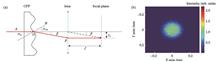
ObjectiveInertial confinement fusion (ICF) requires uniform incident light distribution, and the continuous phase plate (CPP) modulates the incident wavefront distribution by employing the phase fluctuation on the surface, which can realize the shaping and smoothing of focal spots and improve target light uniformity. However, the actual processing ability and detection accuracy of CPP are limited by the surface gradient, which is related to the shaping and smoothing requirements of the far-field focal spot. The researchers studied the relationship between the surface gradient and the far-field focal spot size by geometric optics, but it is necessary to control the size and energy distribution of the focal spot with the requirement improvement in laser focal spot uniformity and energy distribution in high energy density physical experiments. The different focal spot distributions further increase the complexity of the surface gradient distribution and reduce the processing and detection accuracy of the components. Therefore, it is necessary to study and analyze the influence of focal spot size and energy distribution on gradient distribution, and to obtain the surface shape distribution characteristics to predict the processing performance of CPP.MethodsBased on the theory of the near-field and far-field transmission relationship of the beams, we derive the relationship between surface gradient distribution and far-field focal spot energy distribution, and statistically analyze the relationship between the focal spot energy distribution and gradient distribution. Firstly, the focal spots are divided into three types according to the distribution of different target types and the relationship between the light field distribution of the back focal plane and the target plane, including circular focal spots, elliptical focal spots, and eccentric focal spots, with the G-S (Gauss-Seidel) iterative algorithm adopted to design CPP. Secondly, the characteristic parameters of the focal spots, such as elliptic eccentricity and asymmetry, are proposed to characterize the characteristics of the focal spots, and the influence of the gradient characteristics is evaluated by the characteristic parameters. Then we analyze the distribution relationship between the energy distribution of the three types of focal spots and the corresponding surface gradients by histogram statistical and quantitative analysis. Finally, the relationship between random wavefront distribution and far-field energy distribution is employed to verify the universality of the relationship, and the distribution characteristics of surface periods and amplitude are analyzed.Results and DiscussionsThe results show that the histogram of surface depth gradient distribution is consistent with that of light intensity proportion under different radii of focal spots, and the radius of focal spots determines the gradient distribution range. Meanwhile, the energy distribution of focal spots determines the proportion of gradient distribution, and the theoretical analysis is in accordance with the numerical simulation results. The one-dimensional gradient of circular or elliptical focal spots with uniform energy distribution is normally distributed, the mean gradient is close to zero (Fig. 3), and the gradient variance positively correlates with the focal spot radius (Fig. 4). The gradient value corresponding to the peak CPP two-dimensional gradient of the elliptical focal spot decreases with the increasing eccentricity (Fig. 6), and the gradient corresponding to the peak gradient proportion of CPP with eccentric focal spots rises (Fig. 7). Additionally, the relationship between the random wavefront gradient distribution and its far-field focal spot distribution (Fig. 9) is verified, and the minimum spatial period of CPP positively correlates with the surface depth when the target focal spot is determined (Table 2).ConclusionsThe relationship between the surface gradient distribution and far-field focal spot energy distribution is obtained based on the light field transmission theory, and the histogram of the surface depth gradient distribution is consistent with that of the light intensity under different radii of the focal spot. Meanwhile, the radius of the focal spot determines the gradient distribution range, and the energy distribution of the focal spot determines the proportion of the gradient distribution, with the theoretical analysis consistent with the numerical simulation results. The mean gradient is close to zero and the gradient variance positively correlates with the focal spot radius when the energy is uniformly distributed. The smaller elliptical eccentricity of the focal spot leads to a greater proportion of the large gradient value. Eccentric focal spots also increase the proportion of large gradient values. Additionally, the random wavefront is adopted to verify the generality. In conclusion, the relationship between the surface gradient distribution and far-field focal spot energy distribution is determined, and the research results can help estimate the surface distribution and machining error of CPP, thus providing a new idea for wavefront detection.
Oct. 25, 2024Vol. 44 Issue 20 2005002 (2024)
Xinqing Yi, Yang Liu, Yunjie Teng, Jianhua Liu, Junyao Wang, and Jifeng Zhang
ObjectiveThe photoelectric load system under the airborne platform is the basis of aerial photography, aerial mapping, and aerial communication in China. With the diversified application scenarios, the new photoelectric tracking platform characterized by small volume and shape, hidden and flexible installation mode, and high tracking accuracy is more suitable for applications in the new generation of aviation field than the traditional photoelectric platform. Therefore, a photoelectric tracking platform based on dual liquid crystal polarization gratings (LCPGs) is proposed to meet the above application requirements. Meanwhile, the control method is studied to provide theoretical support and technical references for the new tracking system under the airborne platform.MethodsFirst, the dual-LCPG beam solution model is built with the location information of the target location information. The solution model is divided into the forward model and the reverse model. Forward model solution analysis is the premise and foundation for the application of rotating dual-grating beam pointing. The reverse model is a key one that must be addressed in optical tracking and target-directed applications. To achieve high-precision target tracking of dual-LCPC photoelectric follow aim systems, we design a controller combining the solution model and MPC based on the beam solution model. Meanwhile, by employing the servo system controller of dual-grating control, beam deflection, and target tracking, MPC can predict the system model in the future for a certain time to improve the tracking accuracy. Finally, to verify the tracking performance of the system, we build the platform as shown in Fig. 4 for dynamic tracking experiments. Employing dual-grating diffraction characteristics, we place the two gratings in parallel by the servo motor, with the encoder displaying the angle position information of the motor as the feedback signal of the control system. After the incident beam diffraction, the deflection angle is derived from the positive and negative solution calculation model. Additionally, the outgoing beam is received by the camera after the beam, and the image processing unit can process the target off amount. Then, the feedback platform position attitude of the inertial measurement unit is installed on the platform. After establishing the experimental platform, the dynamic tracking accuracy under 2°@0.5 Hz and 5°@0.2 Hz interference respectively. Finally, the overhead time is tested.Results and DiscussionsAccording to the disturbance in the simulated aircraft flight, the maximum angular velocity and angular acceleration are calculated, and similar sinusoidal signals of 2°@0.5 Hz and 5°@0.2 Hz are selected to simulate the airborne disturbance. Therefore, the photoelectric tracking platform is mounted on the six-degree-of-freedom swing platform, and the swing platform is set up simultaneously by swinging around the X axis and the Z axis, with the sinusoidal sine phase difference of 90°. The experimental system is shown in Fig. 5. To verify the tracking effect of the MPC controller, we select the traditional control algorithm PID, and apply the PID controller and the MPC controller respectively to track the target, with the spot stable tracking shown in Fig. 6. The experimental results are shown in Figs. 8 and 9. By adopting the upper machine to record 3000 orientation and elevation target data, the statistical tracking accuracy RMS values of the system under the case of biaxial 2°@0.5 Hz and 5°@0.2 Hz perturbation are 132.56 μrad and 126.69 μrad respectively, and the system tracking performance is significantly improved compared with the traditional PID algorithm.ConclusionsBy studying the tracking performance of a dual-grating photoelectric tracking platform based on the MPC algorithm, the dual-grating beam solution model is built and introduced into the servo control system. The MPC controller is designed to realize the high-precision tracking of the target under the dynamic platform. The experimental platform is built to verify the dual-grating tracking platform. The experimental results show that the MPC algorithm improves the tracking accuracy by more than 23.76% compared with the traditional PID algorithm, and the tracking accuracy is less than 150 μrad. The experimental results verify the effectiveness and excellence of the dual-LCPC photoelectric tracking system based on the MPC algorithm. The results prove that the system can realize high-precision dynamic tracking under the airborne platform. Additionally, the system has sound application significance and provides certain theoretical references and technical support for the development of new light and miniaturized photoelectric tracking technology.
Oct. 12, 2024Vol. 44 Issue 20 2006001 (2024)
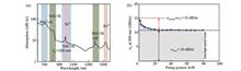
Mengyao Zhang, Yuncong Yang, Lei Gao, Gangding Peng, Tao Zhu, and Qiancheng Zhao
ObjectiveWith the rapid development of science and technology, the demand for data traffic has increased greatly in recent decades. The current optical fiber communication system has been unable to meet the growing demand for network data transmission, and there is a notable gap in the operating band of 1150?1500 nm. Bismuth-doped quartz fiber can achieve ultra-broadband luminescence in the ranges of 1150?1500 nm and 1600?1800 nm, compensating for the spectral gap of existing rare-earth-doped fibers. However, the practical application of bismuth-doped fibers still faces some challenges. To enhance the broadband spectral performance of bismuth-doped fibers (BDFs) in the near-infrared region, various post-processing methods have been proposed. Among these, heat treatment is considered one of the key factors affecting the spectral performance of BDFs, with the extent of the effect depending on the specific heat treatment parameters. To date, there have been no sufficient reports investigating the effects of specific heat treatment processes and parameters on the spectral performance of bismuth-doped alumino-silicate optical fibers at near-infrared short wavelengths (1100?1300 nm). Therefore, we systematically investigate the effects of different heat treatment parameters on the spectral properties of BACs in bismuth erbium co-doped fibers (BEDFs) and determine the optimal heat treatment process and parameters for bismuth-doped alumino-silicate fibers, which is of great significance for their practical applications in fiber optic communications, sensing, and detection.MethodsFirstly, the broadband small-signal absorption spectra of BEDFs are measured using the cut-back method to determine the absorption bands of different active centers, and the pump absorption of BEDFs at 830 nm is also measured. Then, a backward luminescence measurement for BEDFs with various thermal treatments is built, and the effects of thermal quenching and annealing, heating temperature and quenching times, and heating duration on the luminescence spectral characteristics of BACs are sequentially investigated. This process aims to derive the optimal heat treatment process and parameters for bismuth-doped alumino-silicate optical fibers step by step. At the same time, to evaluate the actual small-signal amplification capability of the BEDFs used in this paper, a counter-propagating on-off gain measurement is built to explore the effects of the optimal heat-treatment parameters derived from the above experiments on the gain performance of the BEDFs in the near-infrared band. Finally, the mechanism of the effects of heat-treatment parameters on the spectral properties of the BACs in the BEDFs is discussed in terms of thermally induced and unsaturated absorption variations.Results and DiscussionsFirst, the broadband small-signal absorption spectrum of the BEDF is measured, which contains three groups of absorption peaks (BAC-Al, BAC-Si, and Er3+). The unsaturated absorption of the fiber accounts for 67% of the total small-signal absorption at 830 nm (Fig. 1), indicating that the BEDFs to be tested have a high background loss. Then the effects of different heat treatment processes (thermal quenching and annealing, heating temperature and quenching times, and heating duration) on the luminescence spectral properties of BACs are analyzed and compared. It is found that after thermal quenching, the peak emission intensity of BAC-Al, with its emission peak at 1140 nm, increases by nearly 1.4 times (Fig. 3). Moreover, an excessively slow cooling rate could lead to elevated background loss levels. At heating temperatures of 400 and 500 ℃, successive and repeated quenching further promotes the enhancement of peak luminescence intensity of BAC-Al and gradually saturates, with a maximum increase of up to 1.4 times (Fig. 4). The effect of heating time on the peak luminescence intensity of BAC-Al is further investigated. The luminescence enhancement of BAC-Al at 1140 nm is maximized at a heating time of 2 min with a maximum increase of up to 1.8 times (Fig. 5), However, the background loss level of BEDF continues to accumulate after prolonged heating, reducing the overall near-infrared luminescence emission level. Meanwhile, the luminescence emission spectra of BACs are significantly enhanced between 1000?1350 nm when the heating time exceeded more than 5 min (Fig. 6). The small-signal gain spectra of BEDF at 900?1600 nm are tested, showing a broadband gain of 1250?1600 nm (amplification of stimulated radiation of BAC-Si at 1400 nm and Er3+ at 1536 nm) and significant excited state absorption at 900?1250 nm (ESA of BAC-Al at 1050 nm) (Fig. 8). The luminescence decay curves of BAC-Al under different heating duration are measured, and the luminescence lifetime decreases sharply with increased heating duration (Fig. 9). Finally, it is found that when the heating duration reaches 2 min, the background loss increases insignificantly in the heat induced loss spectra; when the heating duration reaches 20 min, the heat induced loss coefficients have a significant elevation and increase with the decrease of wavelength (Fig. 10). Meanwhile, when the heating duration is less than 2 min, the saturable absorption level increases significantly, representing a significant increase in BACs; when the heating duration is more than 2 min, the increase in the unsaturable absorption (the background loss) becomes predominant as the bismuth clusters form.ConclusionsRapid cooling of bismuth-doped fibers after heating helps to avoid the accumulation of background loss and increase the concentration of BACs. That is, the thermal quenching process improves the working environment of BEDF. The activation temperature of BAC-Al is about 500 ℃, and the optimal heating duration at 500 ℃ is 2 min, which can enhance the peak near-infrared luminescence intensity at 1140 nm by up to 2 times. A prolonged heating duration not only leads to an increase in the bismuth clustering effect but also changes the spectral shape of BAC-Al, and increases the background loss.
Oct. 12, 2024Vol. 44 Issue 20 2006002 (2024)
Ruicheng Zhao, Jianping Li, and Yuwen Qin
ObjectiveDue to their excellent properties, optical frequency combs (OFCs) have been utilized in numerous fields recently, including optical communication, spectroscopy, and microwave signal processing. The features of OFCs, such as broad spectral coverage, flat comb lines, and adjustable frequency spacing, remain the most challenging and desirable aspects to address. The bandwidth of traditional electro-optical modulation-based OFCs is limited to a few tens of nanometers. Combining highly nonlinear fiber with effective nonlinear parametric mixing is the most attractive method for spectral broadening and has been widely studied. However, there is still room for improvement in the spectral range of the demonstrated OFC. To extend the spectral coverage, we propose and experimentally demonstrate a femtosecond all-fiber ultra-wideband electro-optical frequency comb seeded from a 12.5 GHz electro-optically modulated pulse and highly nonlinear fiber, using joint time-frequency pulse reshaping technology. We have realized an OFC bandwidth with a 10 dB power variation over 145 nm, encompassing more than 1450 comb tones and covering the most-used S, C, and L bands. This result enhances the potential of such OFCs in multiband optical fiber communications.MethodsThe all-fiber ultra-wideband electro-optical frequency comb proposed in this study is mainly based on an electro-optical seed frequency comb and highly nonlinear fiber, complemented by joint time-frequency pulse reshaping technology. This configuration consists of three modules: the seed comb module, the joint time-frequency pulse reshaping module, and the nonlinear broadening module. The seed comb module primarily utilizes electro-optical modulation to generate the seed comb, which is composed of electro-optical intensity modulator, phase modulator, and their respective driving modules. The intensity modulator and phase modulator collaboratively control the flatness and width of the frequency comb, respectively. The second module reshapes the pulse in both the time and frequency domains. In the time domain, a nonlinear-optical loop mirror is employed to suppress the pedestal and parasitic sidelobes resulting from pulse compression. In the frequency domain, noise and pedestal components in the low-power spectrum are first reduced through filtering, optimizing the pulse shape. Subsequently, precise dispersion control ensures balance across all modules. The joint time-frequency pulse reshaping method achieves high shaping efficiency with minimal module count. The final module amplifies the pulse peak power and broadens the OFC spectrum using highly nonlinear fiber via parametric mixing. Through meticulous system configuration optimization, electro-optical frequency comb generation has been realized.Results and DiscussionsThe results of the generated comb are shown in Fig. 7 with different resolutions. At a resolution of 0.02 nm, under the condition of 10 dB flatness, the optical frequency comb coverage exceeds 145 nm, meaning the number of carriers exceeds 1450 [Fig. 7(a)]. Meanwhile, the detailed spectral parts covering different bands are shown in Fig. 7(c). These show spectra of more than 350 tones in the C-band within 6 dB flatness, 200 tones in the S-band within 2 dB flatness, and 450 tones in the L-band within 5 dB flatness. At a resolution of 0.2 nm, the calculated optical signal-to-noise ratio (OSNR) is greater than 45 dB, as shown in Fig. 7(b). In addition, the measured average power of the comb is over 2.3 W, corresponding to an average power per comb line of roughly 0 dB. Since the zero-dispersion wavelength of the highly nonlinear fiber (HNLF) used is near 1675 nm, the OSNR in the long-wave part is higher. Moreover, due to the dominant self-phase modulation effect in the nonlinear spectrum broadening process, the spectral flatness, especially in the central regions, should be further improved. Using a polarization-maintaining all-fiber design, including the shaping module, the HNLF, and a high-power optical amplifier, is a better choice to strengthen the flatness of the generated electro-optical frequency comb.ConclusionsAn all-fiber ultra-wideband electro-optical frequency comb covering the most used S, C and L bands is proposed and experimentally implemented in this study. Based on the electro-optical modulated seed optical comb with a center wavelength of 1.5 μm and a frequency spacing of 12.5 GHz, this optical frequency comb generation is realized using joint time-frequency pulse reshaping technology to optimize the femtosecond pulse after compression. This includes frequency domain amplitude control and precise compensation of dispersion. As a result, the pulse pedestal and parasitic sidelobes are well suppressed. This demonstration has achieved a frequency comb output with a 10 dB power variation over 145 nm, corresponding to more than 1450 comb tones. Meanwhile, the measured average power of the comb is over 2.3 W, which corresponds to an average power per line of roughly 0 dB. This power level of a single-frequency comb is sufficient for optical signal transmission. Therefore, the experimental results show that the proposed all-fiber ultra-wideband electro-optical frequency comb has the potential for next-generation ultra-large multiband optical fiber communication and ultra-fast parallel signal processing, among other applications.
Oct. 12, 2024Vol. 44 Issue 20 2006003 (2024)
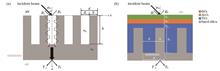
Kun Chen, Mengmeng Guo, Shenghui Shi, Dan Qin, Binbin Luo, Shanghai Jiang, Mingfu Zhao, Huan Tang, Bowen Tan, Tao Song, and Nianbing Zhong
ObjectiveCultural relics serve as tangible remnants of human activities and invaluable cultural heritage passed down from ancient to modern societies. They encapsulate diverse aspects of human life and culture, encompassing social systems, economic activities, technological advancements, and ideological frameworks. Among these relics, paper artifacts stand out as crucial carriers of ancient art, culture, and historical narratives, representing irreplaceable cultural reservoirs. Under suitable environmental conditions such as optimal temperature and humidity, fungi secrete enzymes to hydrolyze these nutrients, facilitating their growth and reproduction. Notably, Trichoderma longibrachiatum, a species within the genus Trichoderma, can thrive, posing a significant threat to paper-based cultural relics. Current methods for detecting mold on paper cultural relics predominantly employ offline and online detection techniques. However, these detection methods often necessitate the use of large analytical instruments, which can potentially damage the artifacts and are time-intensive. Additionally, some methods require direct contact with the artifacts, posing further risks of harm. In this study, we propose the development of a reflective concave stepped inclined lens fiber optic sensor designed specifically for detecting mold growth on the surface of paper cultural relics. This sensor aims to effectively identify and monitor the presence and proliferation of Trichoderma longibrachiatum on paper artifacts, offering promising applications in mold control for paper-based cultural heritage preservation.MethodsThe reflective concave stepped inclined lens fiber optic sensor design features a central incident fiber and an arrangement of 6 and 12 receiving fibers in the inner and outer layers, respectively. The end faces of these receiving fibers adopt both flat and inclined plane structures. Firstly, the detection principle of fiber optic sensors is established, and the influence of sensor structural parameters (such as incident fiber radius, receiving fiber radius, and receiving fiber end face tilt angle) on the detection sensitivity of the sensors is explored. Next, based on the simulation outcomes, the optimal performance fiber optic sensor is fabricated using large core diameter single clad quartz fibers, with core and cladding materials comprising pure quartz and silicone rubber, respectively. The fibers possess core diameters of 400 and 300 μm, cladding diameter of 40 μm, a numerical aperture of 0.22±0.02, an operating temperature range spanning -50 to 250 ℃, and a spectral transmission range of 200?1100 nm. Experimental validation involves cultivating Trichoderma longibrachiatum on tissue paper and rough edge paper substrates lacking ink or dye, using a glycerol nutrient solution and various fungal spores to achieve the required concentrations of fungal spore suspensions. The growth of Trichoderma longibrachiatum is characterized using a super depth of field three-dimensional microscope, and the online nondestructive detection of the growth process of Trichoderma longibrachiatum is carried out using the fabricated fiber optic sensor.Results and DiscussionsThe simulation results highlight the critical impact of outer receiving fiber inclination angle and incident/receiving fiber radii on sensor performance. With the outer receiving fiber at an inclination of 70° (Fig. 4) and the radii of the incident fiber and the receiving fiber of 200 and 150 μm respectively (Fig. 5 and Fig. 6), while keeping other parameters constant, the sensor receives the maximum light intensity. Experimental findings demonstrate that by positioning the optimal reflective fiber optic sensor 2.5 mm from the mold growth on the sample surface (Fig. 8), we can capture the maximum light intensity. Characteristic absorption peaks of Trichoderma longibrachiatum on tissue paper and rough edge paper, both before and after ink dyeing, are consistently observed at 270 nm (Fig. 10 and Fig. 12), with absorbance linearly correlating with mold growth height. Characterization using a super depth of field 3D microscope reveals denser Trichoderma longibrachiatum growth on ink-dyed paper surfaces, fueled by gum and organic matter within the ink, providing rich growth substrates for fungi. Sensor sensitivity for detecting Trichoderma longibrachiatum on cotton paper and rough edge paper before and after ink dyeing is quantified at 9.3×10⁻⁴ AU/μm (Fig. 10, cotton paper before ink dyeing), 10.4×10⁻⁴ AU/μm (Fig. 12, rough paper before ink dyeing), 10.4×10⁻⁴ AU/μm (Fig. 14, cotton paper after ink dyeing), and 11.4×10⁻⁴ AU/μm (Fig. 14, rough paper after ink dyeing), respectively. Compared to single-layer reflective fiber sensors with flat fiber end faces used for detecting Aspergillus niger and Aspergillus fumigatus, our sensor demonstrates approximately twice the detection sensitivity.ConclusionsThis study introduces a novel reflective fiber optic sensor for detecting the growth of Trichoderma longibrachiatum on paper cultural relics. Our experimental results demonstrate the sensor’s capability for online, non-contact detection and precise identification of fungal growth on paper artifacts both before and after ink dyeing processes. The sensor is straightforward to manufacture and offers effective support for mold prevention and control in cultural heritage conservation. Additionally, it broadens the application of fiber optic sensing technology in the field of cultural relic protection, contributing to the advancement of preservation technologies.
Oct. 25, 2024Vol. 44 Issue 20 2006004 (2024)
Maoqing Chen, Yiyang He, Chi Zhang, Zhouyang Lin, Qiang Liu, and Yong Zhao
ObjectiveWhispering gallery mode (WGM) optical microcavity is recognized for its high sensitivity and quality factor, making it invaluable in fields such as fundamental physics and biochemistry. However, traditional fabrication methods pose several challenges, including issues with chemical etching processes on silicon substrates that can adversely affect other optical devices and present health hazards. We address these challenges by employing a three-dimensional (3D) printing technique using two-photon polymerization to fabricate the sensor. This method offers high processing resolution, low fabrication costs, excellent repeatability, and sensitive sensing capabilities, presenting a viable solution for designing and manufacturing high-quality WGM microcavities. In addition, traditional preparation materials such as glass and crystal are limited by glass’s restricted tunability and crystal’s high processing costs. By utilizing polymer materials, our study overcomes these limitations and enhances the sensitivity of the sensor.MethodsWe use Lumerical Mode Solution software to simulate the optical field in the coupling region. The results show that the coupling gap of 100 nm could achieve the ideal resonance effect under the selected waveguide size. The proposed micro-ring resonator is prepared on silicon substrate by two-photon polymerization 3D printing technology with suitable laser intensity and scanning speed, and developed by propylene glycol methyl ether acetate solution and isopropyl alcohol solution. After cleaning the input and output optical fibers with a cutting knife and an optical fiber welding machine, the conical waveguides are precisely aligned using a six-dimensional displacement platform. The structure is then solidified with ultraviolet (UV) glue under ultraviolet light.Results and DiscussionsThe supercontinuum light source and spectrograph are connected with the cured package structure, and the transmittance spectra in the air are 8.96 nm and 14.0 dB respectively. The structure is placed in a temperature and humidity-controlled chamber and tested across a temperature range of 5?35 ℃. The linear fitting results of the transmission spectrum show that the structure has a good linear temperature sensitivity of 243 pm/℃ in the measured temperature range (Fig. 6), which is 2?3 times higher than that of the same type of structure and close to the temperature sensitivity of the cascaded micro-ring resonator. To further explore the salinity sensitivity of the proposed structure, it is placed in a beaker of standard seawater sample solution, and the temperature and humidity are kept constant. When the concentration of standard seawater changes from 20‰ to 230‰, the transmission spectrum of the structure is recorded. The linear fitting results demonstrate good linearity over this range, with a salinity sensitivity of 28.2 pm/‰. These findings highlight the proposed micro-ring resonator's excellent temperature and salinity sensitivity, alongside its compact structure and reproducibility.ConclusionsOur study demonstrates the successful fabrication of a micro-ring resonator sensor on a silicon substrate using polymer materials and two-photon polymerization 3D printing technology. The sensor leverages the strong evanescent field effect of the WGM microcavity and precise wave coupling enabled by the 3D printing process, achieving highly sensitive temperature and salinity measurements. Within a temperature range of 5?35 ℃, the sensor exhibits a temperature sensitivity of 243 pm/℃, significantly outperforming similar structures and approaching the sensitivity of cascaded micro-ring resonators. In standard seawater from 20‰ to 230‰, the salinity sensitivity is 28.2 pm/‰. This kind of optical sensor, characterized by its compact design, high sensitivity, and ease of fabrication, shows considerable potential for applications in fundamental physics, biochemistry, and related fields.
Oct. 25, 2024Vol. 44 Issue 20 2006005 (2024)
Zhiyao Zhang, Chao Gao, Xiaoqian Wang, and Zhihai Yao
ObjectiveSingle-pixel imaging is an indirect imaging technique that uses only one detector element instead of an array of imaging sensors to acquire images. Compared to traditional methods, it offers better detection efficiency in scenarios with limited resources or specific environmental conditions. However, the sampling speed and image quality of current single-pixel imaging methods are insufficient for practical applications. To address this, improvements in sampling methods are needed to reduce time costs while obtaining high-quality images—specifically, optimizing the calibration and sampling strategy to enhance the speed of single-pixel imaging. Many research institutes and universities, both domestically and internationally, have investigated single-pixel imaging sampling and achieved significant results. After continuous innovation and optimization of the sampling method, the sampling rate has decreased under the same signal-to-noise ratio, and the sampling time has been markedly reduced. However, previous research has neglected the processing of non-essential coefficients. When focusing on sampling important regional information, concentrating solely on important coefficients can lead to sampling lag for local information within those regions. Prioritizing the sampling of important coefficients first, followed by non-essential coefficients, can help restore the important regions more completely. Based on this, we propose a new method to tackle these shortcomings and reduce the number of samples required for imaging while ensuring image quality.MethodsThe two-dimensional reflectance spatial distribution function of the target object is first converted into wavelet coefficients using the Haar wavelet transform, which reveals its energy distribution at different frequencies and scales. Initially, based on the information available about the measured target, each scale is assigned an orthorhombic diagonal diameter and subsequent sampling is performed within this orthorhombic area. In the pre-subsampling step, the number of subsamples is set for wavelet coefficients at each scale: the number of sampling points for low-scale coefficients (1st to 4th levels) is either minimal or sampled fully, while the number of high-scale coefficients (5th level and above) is reduced. Finally, random subsampling of the target object is performed. The wavelet coefficients collected through subsampling are first arranged according to the absolute values of their magnitudes, and the corresponding subsampling points are determined to guide subsequent sampling. Next, the remaining wavelet coefficients are sorted in terms of their sampling order. For each scale from the first to the eighth level, the subsampling coefficients are arranged by the absolute value, and sampling points are expanded accordingly. Repeated sampling points are skipped, and the remaining points are sampled to complete the process. All points are then sorted and organized to create a new sampling order for further sampling. In this paper, the peak signal-to-noise ratio (PSNR) of the reconstructed image using the proposed algorithmic sampling method is compared to that of the reconstructed image with standard sampling. The difference in PSNR values is used as the evaluation index.Results and DiscussionsThe comparison of reconstructed PSNR differences shows that the proposed method significantly outperforms the orthogonal sampling one with the same number of samples (Figs.5 and 8). The detail comparison figures for landscape and people images (Figs.7 and 11) further illustrate that, with the same number of samples, the proposed method excels in image reconstruction, particularly in preserving detail. This method requires fewer samples to achieve reconstruction, which maintains the main features and structure of the original image while providing a clearer and more natural effect at the detail level. Consequently, it reduces the computational and storage resources needed and allows for more valuable data acquisition within the same timeframe. Our method notably boosts data acquisition efficiency, enabling effective and accurate data collection even with limited resources.ConclusionsSingle-pixel imaging can accurately reconstruct an image with a small amount of sampling data. We put forward a subsampling fast single-pixel imaging method based on sample reordering. It guides the subsequent sampling order by wavelet subsampling and devises an ordering strategy from the results of random subsampling at each image scale in the previous stage. Theoretical analysis and simulations show that, with the same number of samples, the proposed method considerably improves the signal-to-noise ratio and strengthens imaging efficiency. However, the method is highly dependent on pre-subsampling, which requires continual optimization. Future research should focus on mitigating the effects of pre-subsampling and exploring additional optimization strategies to strengthen the robustness and applicability of the method in real imaging scenarios.
Oct. 11, 2024Vol. 44 Issue 20 2011001 (2024)
Yi Zong, Shengyao Sun, Xiyuan Shi, Caiyun Yu, Yixuan Liu, Mingliang Duan, and Jianxin Li
ObjectiveWith the expanding application of large aperture and complex optical systems, the demand for aspheres is also increasing. Aspheres whose surface deviates from the spherical surface prove more design freedom for optical systems than spherical surfaces, and help improve image quality and achieve a compact and lightweight design of optical systems. Without high-precision testing, there cannot be deterministic control and manufacturing. The widespread utilization of aspheres requires high-precision surface measurement as support, and the final manufacturing accuracy is mainly determined by the testing accuracy. Asphere testing has developed numerous solutions, among which non-interference methods usually have sound flexibility without high measurement accuracy, and some methods are contact measurement, which can easily damage the device under test. Interferometric measurement methods include null and non-null interferometry, among which null interferometry has limitations in measuring the dynamic range and flexibility. Non-null interferometry lowers the high requirements for wavefront compensation, thereby improving the dynamic range and universality of measurement. The subaperture stitching interferometry is the most widely employed among non-null interferometry. The combination of subaperture stitching interferometry and partial compensation can achieve high-precision and flexible asphere testing. We propose an aspheric subaperture stitching interferometry with a single-wedge variable compensator to provide a new solution for high-precision testing of aspheres.MethodsThe proposed method is an aspheric subaperture stitching interferometry with a single-wedge variable compensator, which can be adopted for flexible asphere interferometry. The standard converging spherical wave emitted by the interferometer is modulated by an optical wedge to reach the subaperture of the tested asphere. The optical wedge can realize translation and rotation along the optical axis direction. The scanning system includes modules of subaperture scanning and component alignment. During measurement, the direction of the output beam is changed by altering the axial position of the optical wedge to complete radial scanning of the subaperture ring from the center to the edge and reduce the motion complexity of the scanning module. Meanwhile, the spherical wavefront after being modulated by optical wedges can compensate for fundamental aberrations such as astigmatism and coma of asphere subapertures. All subapertures of aspheres are collected by tilting and rotating the optical wedge around the axis. Reverse optimization reconstruction is utilized to correct system return error and projection distortion for all subaperture data. Afterwards, the stitching algorithm using alternating calibration is employed to reconstruct the phase distribution with the subaperture data after system error correction.Results and DiscussionsThe stitching algorithm using alternating calibration is utilized to obtain the full-aperture phase of the tested asphere. The six-dimensional positioning error obtained by stitching is shown in Table 2. The measured low-frequency phase of the tested asphere is shown in Fig. 16(a), and the peak-valley (PV) value and root-mean-square (RMS) are 0.4283λ and 0.1070λ respectively. The residuals of the proposed method and LuphoScan 260 are shown in Fig. 16(c), and the PV and RMS are 0.1259λ and 0.0273λ respectively. The phase distribution and residual show that the proposed aspheric subaperture stitching interferometry with a single-wedge variable compensator can achieve measurement accuracy of approximately λ/8 (PV) for aspheres. The distribution of residuals is close to coma, and this may be caused by the following three reasons. Firstly, when a single optical wedge for asphere compensation stitching interferomety is employed, the optical wedge mainly compensates for the astigmatism and coma of the off-axis subaperture. In actual testing, the processing and installation errors of the optical wedge can cause the aberration compensation of the subaperture to deviate from the ideal design testing state, resulting in measurement errors. Secondly, it is necessary to align the testing system and ensure that the motion of the test mirror controlled by the scanning system during subaperture scanning measurement conforms to the subaperture planning route. In this experiment, the test mirror may tilt in the vertical direction, which usually introduces coma in the test phase. Thirdly, there are residuals in the calibration of the system retrace error and projection distortion, which are coupled into the retrieves phase. These problems will be our focus in the future.ConclusionsWe propose an aspheric subaperture stitching interferometry with a single-wedge variable compensator, providing a new solution for high-precision and flexible asphere testing. This method employs a single optical wedge as a subaperture aberration compensator, and compensates for the basic astigmatism and coma of the off-axis subaperture by adjusting the tilt angle of the optical wedge. Meanwhile, adjusting the axial position of the optical wedge can also achieve subaperture scanning at different off-axis positions. Finally, the stitching algorithm is adopted to complete the full-aperture phase reconstruction. Additionally, we analyze the wavefront aberration modulation mechanism of the optical wedge and propose a complete alignment method for the optical wedge pose system. The experimental results show that the proposed method has good consistency with the point scanning results of the 3D profilometer, and the full-aperture testing residual is about λ/8 (PV). This indicates that the proposed method can yield high-precision asphere compensation stitching interferometry, and has a simple and flexible compensation structure, thus improving the measurement ability of subaperture stitching interferometry.
Oct. 12, 2024Vol. 44 Issue 20 2012001 (2024)
Chen Zhou, Xinjun Wan, Xiaoxiao Wei, Zhenqiu Dai, and Xiaobin He
ObjectiveWhite light scanning interferometry (SWLI), as a high-precision, non-contact measurement technique, is widely used in fiber optics, automotive industry, precision measurement, and manufacturing. SWLI can employ piezoelectric ceramics (PZT) or stepper motors for vertical scanning. Although PZT features extensive application due to its high precision, it requires expensive controllers to correct the hysteresis effects brought by the piezoelectric elements. Additionally, the range of PZT is typically limited to several tens of micrometers. In contrast, high-precision stepper motors used for axial scanning provide a broader range and reduce cost. However, the nonlinear stepping vibrations of stepper motors lead to greater displacement errors than PZT, resulting in significant random errors between the spacings of adjacent frames of interferometric images. This issue can cause obvious ripple errors or height jumps in morphology calculations, resulting in lower solution accuracy and challenges for SWLI in cost reduction and measurement in vibrating environments. The elimination of this problem will enhance the applicability and accuracy of SWLI technology, further advancing its development and application across various fields.MethodsWe improve and further investigate the fitting compensation techniques proposed by previous researchers. A stepper motor is used as the scanning component to support the objective lens in vertical displacement. A high-precision grating ruler is installed on the guide rail to directly read the displacements accurately and sort the signals. The sorted interference signals are then coarsely positioned at the center of the zero-order fringe using the centroid method. Additionally, non-equidistantly sampled signals undergo trigonometric fitting using the Fourier series. By randomly sampling several coordinate points of the interference images, optimal angular frequency parameters are determined using a search algorithm, followed by matrix calculations and signal set fitting using the linear least squares method. Based on the coarse positioning, an appropriate interval is selected for high-density up-sampling of the fitting function. This interval can range between one-quarter to one-half of the wavelength to ensure coverage of the coherent peak waveforms in the interference signal, thus obtaining accurate coherent peak positions and reconstructing the object’s morphology (Fig. 3). We adopt an approach of up-sampling specific local areas to reduce computational load and enhance measurement accuracy.Results and DiscussionsWe conduct both simulation experiments and actual measurement tests. In the simulation experiments, tests are carried out using simulated scanning with vibration errors. The simulated white light Gaussian source has a central wavelength of 550 nm and a spectral width of 100 nm, with a scanning step size set at 40 nm and a simulated step height of 400 nm. Certain random errors are introduced in the vertical scanning intervals, with the range of single displacement errors within 40%, and Gaussian noise is added. The centroid method and the proposed algorithm are compared, with the results of morphology restoration and errors shown in Fig. 7 and Fig. 8. Repeated measurements indicate that the error rate decreases from 3.5% to 0.11%. In the actual measurement experiments, a microscope driven by a white LED light source and a stepper motor is used to test step samples. The displacement error and test results are shown in Fig. 11. The comparison shows that our algorithm, compared to the original one, better controls the calculation errors caused by defect signals due to nonlinear sampling in the actual measurement environment. Table 2 shows the computational errors of various algorithms for the step samples, where the error rate of the proposed algorithm decreases from 1.32% to 0.36%.ConclusionsWe introduce an improved white light interferometry algorithm adapted for non-equidistant sampling environments. The algorithm begins with coarse positioning of the interference coherence peak to define the local sampling interval. Optimal angular frequency parameters obtained via the proposed algorithm are then used for least squares matrix fitting of the signal. Subsequent high-density up-sampling within this interval allows accurate determination of the zero optical path peak signal points, thus precisely defining the sample’s surface morphology. Both simulation and experimental results demonstrate that this algorithm effectively reduces ripple errors caused by non-equidistant signal distribution in vibrating environments and effectively reduces calculation errors due to decreased interpolation performance compared to the original algorithm. Characterized by high accuracy and repeatability, this method also significantly reduces the computational burden of up-sampling all signals by sampling selected regions, making it an efficient 3D reconstruction algorithm for white light interferometry.
Oct. 12, 2024Vol. 44 Issue 20 2012003 (2024)
Fangchao Zhai, Qinghua Zeng, Feilong Mao, Helong Wang, and Jie Li
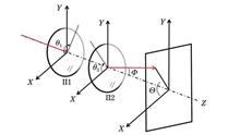
ObjectiveThe photoelectric stabilization platform is a system that integrates optical and electronic technology to achieve stable and precise target tracking and positioning. A stable platform with a reflector, in combination with a mechanical stabilization frame and the reflector itself, ensures line-of-sight stability. Owing to the lower inertia of the reflector, it offers enhanced stability. Biaxial reflectors occupy less space but present higher complexity due to nonlinear coupling and control. Traditional methods approximate the mirror’s motion characteristics over its entire range as those near the zero position, which is suitable for small, slow compensation movements but introduces significant errors for larger, faster motions. This study requires high-resolution imaging when the mirror has a large compensation range and a fast speed, necessitating precise motion analysis of the mirror. Previous work deduced the relationship among the direction vector of the aiming line, the angle of the aiming line, and the angle of the reflector, accurately describing the reflector’s behavior during extensive movements. However, the derived relationship remains nonlinear, and considering the optical path and platform movement of the optoelectronic stabilization platform, the problem complicates the issue further.MethodsThe nonlinear relationship between the position of the aiming line and the angle of the reflector typically necessitates simplification to obtain analytically accurate results. The nonlinearity fundamentally arises from the non-straightness of the reflection transformation group and the attitude transformation group. Therefore, our study employs Lie group theory for analysis. The properties of the entire Lie group can be characterized by the tangent space at the identity element, known as the Lie algebra. Using Lie algebra allows us to capture the linear properties of Lie groups near any element, not just at the identity. We introduce the virtual image motion analysis (VIMA) method, which analyzes the motion of the aiming line through the movement of the virtual image of the sensor along the direction of the aiming line. The relationship between the speed of the aiming line and the angular velocity of the reflector is determined using the Lie group and the Lie algebra method. This method directly solves the angular velocity of the reflector and integrates this to find the reflector angle. Since no simplifications are made, only discrete errors occur, significantly enhancing solution accuracy.Results and DiscussionsWe test the compensation effect of the reflector by measuring the error between the actual line of sight compensated by the reflector and the commanded line of sight, as well as the permissible motion range of the reflector using two techniques. The platform moves according to a specified angular velocity excitation signal, and the reflector must compensate for this motion to keep the unit vector of the aiming line stable within the geographic framework. Results from Figs. 3?6 show that the VIMA reduces error by three orders of magnitude compared to traditional reflection vector methods, validating our assumptions and deductions. Table 1 indicates that the worst-case permissible motion range for the simplified reflection vector method is 4.76°, whereas the virtual image motion analysis method did not reach the permissible error throughout the simulation, allowing for at least a 35.98° motion range—a significant improvement over the simplified method.ConclusionsBased on Lie algebra theory, our study analyzes the reflector movement in optoelectronic stabilization platforms. We propose the VIMA to describe the relationship between the velocity of the line of sight and the angular velocity of the reflector. The VIMA enables direct resolution of this relationship to determine the angular velocity of the reflector, with its angle obtained through integration. This effectively addresses the nonlinear challenges of traditional reflection vector methods. The VIMA eliminates simplification errors, reducing image motion compensation errors by three orders of magnitude compared to conventional methods. This technique also holds significant implications for image motion analysis in other optical systems and optical system design.
Oct. 12, 2024Vol. 44 Issue 20 2012004 (2024)
Hao Li, Ziyi Liu, Yule Zhao, Qiang Wang, Yanling Xiao, and Hui Liu
ObjectiveTopological photonics, a novel method for controlling light flow, exploits topologically protected photonic states at interfaces between topologically trivial and non-trivial structures. These states can maintain robust light transmission even in the presence of structural defects. An ideal integrated optical platform for realizing topological photonics is lithium niobate on insulator (LNOI). However, the challenges in etching lithium niobate pose a hurdle to achieving mass production. Recently, a new type of LNOI that requires no etching has been proposed. This technology, by avoiding complex etching steps, shows tremendous potential to become the next-generation optical integration platform. Nevertheless, research on topological devices using this platform is still rare. Here, we report the design of a one-dimensional waveguide array using the concept of synthetic dimensions. This design enables the coherent coupling of topological interface states between multiple layers of three-dimensional Weyl lattices by adjusting the relative twist angles between different Weyl lattices. We aim to flexibly control light output by designing waveguide arrays of different lengths, thereby enriching the freedom of light control. This approach provides new design ideas for the integration of large-scale photonic devices on chips, particularly in the fields of optical switches and logic devices.MethodsWe employ a combination of experimental and theoretical methods to investigate the topological characteristics of Weyl points in thin film unetched lithium niobate waveguide arrays. Theoretically, a tight-binding model is employed to design different waveguide spacings, which are considered synthetic dimensions. This approach aims to realize three-dimensional Weyl points within a one-dimensional waveguide array system. Multiple layers of Weyl lattices are crafted, and by adjusting the relative twist angles between different layers, the coherent coupling of topological interface states is achieved. Experimentally, unetched waveguides are fabricated using electron-beam lithography, which simplifies the production process while still leveraging the nonlinear advantages of lithium niobate. A continuous-wave laser acts as the light source and is transmitted to the waveguide array through optical fibers. Waveguide arrays of varying lengths are tested, and a power meter is utilized to scan the output grating, verifying the coherent coupling of topological interface states.Results and DiscussionsUsing the concept of synthetic dimensions, the theoretical design of a one-dimensional waveguide array confirms that coherent coupling of topological interface states can be achieved by controlling the relative twist angles between multiple layers of three-dimensional Weyl lattices [Fig. 6(a)]. Theoretical calculations indicate that different interface state modes at the output end vary with different propagation lengths, confirming the presence of coherent coupling (Fig. 7). Experimentally, the theoretical design is validated by measuring the output gratings of waveguide arrays of varying lengths (Fig. 9).ConclusionsWe employ a novel thin film unetched lithium niobate system that integrates the concepts of topological photonics and synthetic dimensions to design a large-scale, sub-wavelength scale waveguide array system. By adjusting the waveguide spacing and introducing additional parameter dimensions, a three-dimensional Weyl lattice is constructed within a one-dimensional waveguide array system. This structure exhibits Fermi arc boundary states that extend to the parameter space boundary, enabling the connection of two layers of Weyl lattices through rotational mapping techniques. The relative twist direction determines whether topologically protected interface states exist at the stitching interface. Moreover, the stitching of three-layer twisted Weyl lattices is achieved, and by controlling the twist angles between different layers, coherent coupling of interface states at two interfaces is realized. Using different lengths of waveguide arrays facilitates directional output effects, which have been experimentally validated. Compared to traditional single topological interface states, coherently coupled topological interface states demonstrate greater potential in optical switches and logic devices, thereby opening new avenues for the integration of large-scale photonic devices on chips.
Oct. 25, 2024Vol. 44 Issue 20 2013001 (2024)
Xudong Zhu, Zhaoxian Chen, Xia Meng, Ao Li, Bingxiang Li, Lei Wang, Wei Hu, and Yanqing Lu
ObjectiveTerahertz (THz) technology has broad application prospects in astronomy, security, biomedicine, broadband wireless communication, and other fields. However, the current THz system is bulky and has limited applications. THz integrated photonics is the key to further development and wide applications of THz technology, among which photonic topological insulator (PTI) is a good integration platform. Topological edge states (TESs) in the PTI bandgap have caught extensive attention. They can realize light transmission only along the interface and have no backscattering, with robustness to disorder and defects. Among PTIs, valley photonic crystal (VPC) constructed based on the photonic quantum valley Hall effect do not need to introduce magnetic fields or pseudospins, but only need to break the spatial inversion symmetry, and TESs will be formed on the edge of two photonic crystals with opposite valley Hall phases. However, once a traditional topological photonic device is designed, its functional characteristics are difficult to change. Manipulating the topological phase and realizing dynamic TES tuning will result in breakthroughs for designing THz photonic crystal chips, which becomes a research hotspot in this field. As a soft material with excellent properties, liquid crystals (LCs) are sensitive to external fields such as light, electricity, magnetism, and heat. Meanwhile, it is an ideal method to realize the dynamic control of THz topological devices by dynamically tuning the refractive index of LCs with an external electric field. Conventional LC-based topology devices adjust the TESs or topological angular states by changing the overall topological properties, and they are difficult to fabricate via experiments. Additionally, the study on THz tunable TESs based on local LCs has not been reported.MethodsDifferent from the entire device filled with LCs, we only fill the hole of the topological interface with the LCs and design a tunable THz VPC. Firstly, a two-dimensional photonic crystal is constructed to break the spatial symmetry by changing the duty cycle of the two air cavities to open the bandgap. Then a VPC is constructed, and the tunable TESs are studied. Meanwhile, we construct a Z-shaped waveguide and add LCs after the first bend, further design a forked wavelength division multiplexer (WDM), and add LCs to the upper branch. Additionally, the TES characteristics with different THz frequencies are analyzed, with the effect of a defect on TES transmission studied finally. The refractive index change of LCs at the VPC interface can tune the TES transmission. This transition of TESs breaks conventional bulk-boundary correspondence, which attributes the existence of TESs in VPCs to bulk topology while disregarding the role of the interface refractive index.Results and DiscussionsWe start with the basic properties of THz VPCs (Fig. 1) and pattern the VPCs on a silicon slab. Each unit cell of these VPCs comprises two inequivalent circle holes, R1=0.25a, R2=0.08a. The Dirac point originally located at K(K') is opened, creating a bandgap. Hz phase distributions of the upper and lower bands of VPC 2 and VPC 3 at the K(K') point have opposite directions. The Poynting vector also exhibits vortex properties of opposite chirality (black arrow) along with topological band inversion. VPC 2 and VPC 3 with bandgaps and band inversion will generate TESs at the interface of their composition. The influence of changing the LC refractive index of the interface on edge states in VPC is demonstrated. The projected energy band of the supercell with beard interfaces is calculated (Fig. 2). The dispersion curve of the edge state shifts down, indicating that some operating frequencies no longer maintain TESs. As the LC refractive index increases, the curve shifts down further, but the TES always maintains a frequency range. When the LC refractive index is adjusted under different applied voltages, TESs can be tuned over a certain frequency range (between blue and black dashed lines). At the boundary, the electric field has a local enhancement effect with its direction along the x direction. Then, an LC tunable Z-shaped topological waveguide is constructed (Fig. 3). When the LC is not filled, the waveguide maintains a high transmittance in the range of 0.90?1.03 THz. After the LC is filled and n=1.8, the upper edge of the transmittance curve shifts to low frequency. The passband range rises as the LC refractive index decreases. No matter what the refractive index of the LC is, the THz transmittance is the same at 0.950 THz, while at 1.005 THz, the THz wave has a very different field distribution. At 0.990 THz, the tunable transmission of the TESs in the Z-shaped waveguide and the electric field diagrams is shown (Fig. 4). Additionally, an LC-tunable wavelength division multiplexer (WDM) is designed (Fig. 5). At 0.990 THz and n=1.5, the THz wave passes through the upper branch, and under n=1.7 the THz wave passes through the lower branch. This is consistent with the THz transmission rule of the Z-waveguide above. When n increases from 1.50 to 1.68, the THz wave transmits mainly from port 2, and the transmittance is about 80%. As n increases from 1.68 to 1.80, the output of THz waves is mainly from port 3, and the transmittance is close to 100%. A point defect with no LC added is introduced to the interface and the electric field on the interface at 0.990 THz is shown (Fig. 6). The transmittance spectrum is almost unaffected by the defect. The LC tunable topological photonic devices constructed by pure LCs or dielectric rods have high requirements for LC packaging and manipulation. The VPC structure in our study has sound backscattering immunity and stable mechanical strength. The enhanced THz near-field at the boundary can interact with LCs in the air cavity. Additionally, it is convenient to control the orientation of LCs to change the refractive index by an external electric field, which ensures the TES tunability. We have simplified the LC integration and manipulation methods, which is conducive to follow-up experiments and further research.ConclusionsTHz integrated photonics is the key to further development and widespread applications of THz technology. VPCs are a good platform for realizing integrated devices and their dynamic control is in high demand. We propose a THz VPC with tunable TESs based on LCs, with a focus on the influence of LCs on the topological transmission characteristics. The topology-protected edge state of the Z-shaped waveguide can be dynamically tuned in the range of 0.98?1.00 THz, while the topological transmission characteristics in the range of 0.90?0.98 THz are unchanged, indicating that the device has sound robustness. Additionally, we construct a THz WDM which shows excellent multiplexing properties and defective immunity. In the future, the design can be further optimized to implement programmable broadband THz topology on-chip devices. Therefore, our study plays a significant role in promoting the wider application of PTIs and THz technology, and the results are of significance for a deep understanding of TESs and the development of THz integrated chips.
Oct. 11, 2024Vol. 44 Issue 20 2013002 (2024)
Jun Qin, Junxiong Tan, Yu Sun, Lü Junde, Kejia Zhu, Yueqin Li, Jian Sun, and Min Miao
ObjectiveSilicon photonics is one of the most promising technologies to enable low-cost, low power consumption and high-performance optical transceivers. Compared to Mach-Zehnder modulators (MZMs), silicon microring modulators (Si-MRMs) have attracted significant attention in recent years due to their compact footprint, high modulation speed, and potentially more energy-efficient dense integration for multi-lane data transceivers. However, Si-MRMs are highly sensitive to fabrication process variations and environmental fluctuations, leading to resonance drift and changes in coupling states that degrade signal performance, especially for advanced modulation formats like 4/8-level pulse amplitude modulation (PAM4/PAM8). Despite this, there is a lack of in-depth quantitative analysis on the effect of modulator coupling states on system performance. Typically, MRM parameters such as radius, coupling gap, doped regions, metal contacts, and waveguide dimensions are carefully calculated and chosen to achieve critical coupling. However, during fabrication, testing, or deployment in communication systems, the coupling state of the Si-MRM can shift from critical coupling to overcoupling or undercoupling due to fabrication errors, temperature fluctuations, and applied voltage, affecting system performance. A quantitative investigation into the influence of Si-MRM coupling states on system performance is crucial for modulator design and integration into various systems.MethodsIn this study, we conduct a comprehensive quantitative analysis of the effect of Si-MRM coupling states on a high-speed PAM4 transmission system using a system-level model that includes a dynamic ring resonator model and an equivalent electrical circuit. Performance metrics such as signal bit error rate (BER), receiver side maximum received optical power (RoP), power penalty, device bandwidth, and eye diagram are investigated. Modeling and simulations are carried out in VPI Transmission Maker and Matlab. The dynamic ring resonator model simulates the optical properties of modulators, capturing variations in the optical field within the resonant cavity coupling region and at the input and output ports over voltage and time, as well as adjustments in signal phase and power within the ring waveguide. The circuit subsystem models the effect of voltage on parameters such as resistor, junction capacitance, and inductance, including equivalent circuitry for wire bonding. The MRM model is made of silicon with a depletion-type phase shifter. In the simulation, the MRM radius is set to 10 μm, corresponding to a free spectral range (FSR) of 8.75 nm. The lateral PN junction in the ring waveguide provides varying carrier depletion at different reverse voltages. Doping concentrations for n and pin the low-doped region are 3.5×1018 cm-3 and 6.5×1018 cm-3, respectively, while the high-doped region features a doping concentration of 4.5×1021 cm-3 for both n and p. The measured loaded Q factor of the MRM is ~4655 at a bias voltage of 0 V. The electro-optic (EO) phase efficiency of the PN junction is measured to be 0.56 V·cm at a reverse bias voltage of 2 V. In the simulation, the coupling states of the microring resonator are regulated by manipulating the coefficients a and t, which correspond to the single-pass amplitude transmission factor and self-coupling coefficient, respectively.Results and DiscussionsThe simulation results indicate that for PAM4 generation operating under critical coupling when the data rate of the generated signal is below 150 Gbit/s, incremental variations of a and t from 0.59 to 0.91 lead to a maximum power penalty of 4.2 dB. Optimal system performance is attained when values of a and t range from 0.71 to 0.83. When the modulation speed exceeds 160 Gbit/s and a(t) value is set to 0.91, significant enhancement in system performance can be attained due to increased device bandwidth. In overcoupling and undercoupling states, where the modulation speed remains below 150 Gbit/s and adequate device bandwidth is maintained, variations in t with a constant a or adjustments in a with a constant t result in degraded system performance compared to the critical coupling state. Only slight variations in t (ranging from 0.71 to 0.79, with a maintained at 0.75) or a (ranging from 0.71 to 0.79, with t maintained at 0.75) can yield system performance closely approximating that of the critical coupling state (where a and t are both set at 0.75). When the modulation speed surpasses 180 Gbit/s, achieving BER performance below the threshold of soft-decision forward error correction (SD-FEC) is possible only by increasing the value of a to 0.83?0.91 to enhance the bandwidth. Under these conditions, system performance exceeds that of critical coupling. However, in the undercoupling state, no results have been observed where performance exceeds that achieved under critical coupling conditions.ConclusionsOur study provides a comprehensive and quantitative analysis of the effect of coupling states of Si-MRM on the generation of high-speed PAM4 signals (ranging from 64 Gbit/s to 224 Gbit/s). The entire analysis is based on a system-level model of Si-MRM. In the simulation, different coupling states are simulated by changing the values of a and t, and a quantitative analysis is conducted on key performance indicators, including BER performance, RoP at the receiver, power penalties, device bandwidth, and eye diagrams. The results show that optimal system performance is attained at the critical coupling state, and the bandwidth meets the rate requirement. Within this context, the best system performance is observed when a(t) ranges between 0.71 and 0.83. In scenarios of overcoupling or undercoupling states, where the modulation bandwidth aligns with the modulation rate requirement, variations in t with a constant a or adjustments in a with a constant t result in degraded system performance compared to the critical coupling state. Otherwise, performance below the threshold for BER with SD-FEC is possible only by increasing the value of a to enhance the bandwidth. In this scenario, the overcoupling state exhibits enhanced performance compared to the critical coupling state. However, no instances within the undercoupling state, which involve changes in a, have displayed performance better than that of the critical coupling state. Our study provides valuable insights into the quantitative assessment of Si-MRM coupling state variations caused by fabrication, testing, network deployment, etc., and their consequent effects on the performance alterations of high-speed modulation signals. Such findings are pivotal for directing the development of next-generation 800 Gbit/s和1.6 Tbit/s chip-level high-speed optical interconnects utilizing Si-MRM technology.
Oct. 12, 2024Vol. 44 Issue 20 2013003 (2024)
Qian Tu, Yunhan Zhu, Jianhua Chang, Youpeng Su, and Tianyi Lu
ObjectiveWavelength-tunable and multi-wavelength mode-locked fiber lasers are essential in fields such as communication technology, fiber sensing, and ultrafast photonics. While wavelength tuning is commonly achieved by incorporating additional tunable filters, most of these filters function solely as filters and require separate mode-locking techniques. Recently, the saturable absorber based on graded index multimode fiber (GIMF) has gained attention due to its advantages of easy fabrication, high damage threshold, and strong anti-interference capabilities. It can serve both as a mode-locked device and a filter. In this study, we propose a method featuring a simple structure, high loss threshold, and low insertion loss to achieve wavelength-tunable laser output and dual-wavelength switchable mode-locked pulse output of erbium-doped fiber lasers.MethodsWe propose a graded index multimode fiber-single mode fiber-graded index multimode fiber (GSG) structure, which functions both as a saturable absorber for mode-locking and a filter for wavelength tuning. The GIMF length is fixed at 11.2 cm to align with the self-imaging period, and the GIMF 1 and GIMF 2 have identical parameters to create a symmetrical structure. We theoretically calculate the length range of the single-mode fiber that meets the requirements and conduct comparative experiments within this range. Experimental results show that when the length of the single-mode fiber is between 2.7 cm and 5 cm, the GSG structure functions effectively as a mode-locked device and filter with wavelength tuning capability. We test the GSG structure with a fiber laser and use a digital oscilloscope, optical spectrum analyzer, autocorrelator, radio frequency analyzer, and power meter to measure output pulse characteristics including spectrum, pulse width, repetition rate, and output power.Results and DiscussionsTesting the GSG structure with a fiber laser reveals several key observations. At a pump power of 15 mW, we observe continuous wave output on the oscilloscope. As the pump power increases to 24 mW, we see Q-switched mode-locking. At 46 mW, we achieve a stable mode-locked state, with no pulse splitting or harmonics detected up to the maximum pump power of 289 mW. When the pump power is set to 87 mW, the center wavelength of the pulse is 1558.6 nm, with a pulse width of 0.6 ps and a 3 dB bandwidth of 5.95 nm (Fig. 5). By gradually adjusting the polarization controller, we achieve mode-locked pulse output with tunable wavelengths. The central wavelength of the mode-locked pulse can be stably tuned across the range of 1550.9 nm to 1558.9 nm (Fig. 6). At a pump power of 110 mW, we observe both mode-locked pulse and continuous wave outputs. By further adjusting the polarization controller, we obtain dual-wavelength mode-locked pulse switching at central wavelengths of 1531.6 nm and 1556.2 nm (Fig. 7). In the stable mode-locked state, adjusting the polarization controller alters the transmission characteristics of the GSG structure. These changes affect the wavelength-dependent gain and loss equilibrium points within the cavity and the polarization hole burning effect. Additionally, variations in the distribution of gain peaks in the erbium-doped fiber contribute to wavelength tuning and switching.ConclusionsWe present an all-fiber structure based on GIMF-SMF-GIMF that combines the saturable absorption characteristics of GIMF with the Mach-Zehnder (MZ) filtering effect of the GSG structure to achieve single-wavelength tunable and dual-wavelength switchable mode-locked pulse outputs in erbium-doped fiber lasers. With a polarization controller adjustment, we obtain a mode-locked pulse with a repetition rate of 8.5 MHz, a pulse width of 0.6 ps, a signal-to-noise ratio of 64 dB at 87 mW pump power, and a wavelength tuning range of 1550.9?1558.9 nm. At 110 mW pump power, we achieve mode-locked pulse switching and dual-wavelength mode-locked laser output. The GIMF-SMF-GIMF all-fiber structure, with its simplicity, high loss threshold, and low insertion loss, provides a valuable reference for designing compact, multifunctional fiber laser mode-locked devices.
Oct. 11, 2024Vol. 44 Issue 20 2014001 (2024)
Yanping Yang, Shihan Liu, and Heng Zhou
ObjectiveUltra-narrow linewidth lasers have found widespread application in various fields such as precision gyroscopes, optical sensing, coherent optical communication, atomic clocks, and ultra-stable microwave generators. Recently, researchers have used stimulated Brillouin scattering (SBS) in ultra-high-quality-factor (Q-factor) fiber resonators as an effective method for linewidth compression. By increasing the Q-factor and Stokes light power in a long fiber cavity, the linewidth of Brillouin lasers can be compressed, resulting in a narrower output beam. However, achieving stable single-longitudinal-mode operation with a long fiber cavity can be challenging due to limitations of the free spectral range (FSR), relative to the gain bandwidth of SBS. The Vernier effect in a compound cavity can address this challenge and achieve single-longitudinal-mode operation with narrow linewidth, though this approach requires precise control of cavity lengths and can be complex. In the present study, we described a novel approach that combines the Pound-Drever-Hall (PDH) locking technique with the stimulated Brillouin effect in an ultra-high-Q-factor fiber resonator and achieved a significantly reduced linewidth for Brillouin lasers, reaching the sub-mHz level. We hope that this research will promote the development of narrow linewidth Brillouin lasers and drive progress in several key fields, including optical communication, optical spectrum analysis, and optical sensing.MethodsWe combine the Pound-Drever-Hall (PDH) locking technique with the stimulated Brillouin effect in an ultra-high-Q-factor fiber resonator to compress the linewidth of Brillouin lasers. Initially, we increase the coupled Q-factor to over 1010 by lengthening the fiber resonator and simultaneously reducing its free spectral range. In addition, thermal and mechanical isolation treatments are applied to the fiber resonator with foam and aluminum boxes to mitigate the influence of external environmental factors. The high-precision PDH locking technique is then used to generate a single-longitudinal-mode Brillouin laser with side-mode suppression exceeding 70 dB, even when the FSR of the fiber resonator is significantly smaller than the Brillouin gain bandwidth. Furthermore, we employ three methods to rigorously test the linewidth of the fiber Brillouin laser: the reference laser heterodyne method, the delayed self-heterodyne method, and the common cavity laser heterodyne method. These methods allow us to achieve a fundamental linewidth for the Brillouin laser at the sub-mHz (millihertz) level.Results and DiscussionsAs shown in Fig. 5, the findings indicate that as the Brillouin laser power increases, there is a corresponding increase in side-mode power. Specifically, when the Stokes power is raised to 13 dBm, the Brillouin laser achieves a side-mode suppression ratio of 70 dB. However, further increasing the Brillouin laser power may potentially reduce noise performance. The analysis of the three linewidth measurement methods is shown in Fig. 6. The common cavity laser heterodyne method effectively suppresses common-mode, mechanical, and vibration noise. At a Brillouin laser output power of 9 dBm, the fundamental linewidth is calculated from the frequency noise in the white noise region as 31 μHz, which closely matches the theoretical expectation of 30 μHz. Results from the delayed self-heterodyne method, shown in Fig. 6(b), reveal a fundamental linewidth of 0.9 mHz at a Brillouin laser power of 13 dBm. However, experimental results are significantly influenced by variables such as the delay fiber length and external environmental conditions, which constrain measurement sensitivity and cause a notable deviation from theoretical values. In addition, comparing the phase noise of the Brillouin laser with that of the pump laser under PDH-locked conditions indicates that the Brillouin laser significantly mitigates the frequency noise of the pump light in this specified range.ConclusionsIn this study, we present a significant advancement in laser technology by successfully combining the PDH locking technique with SBS in an ultra-high-Q-factor fiber resonator. The result is a single-longitudinal-mode Brillouin laser with a narrow linewidth and substantial potential across various applications. Our meticulous approach involves three distinct measurement schemes—the reference laser heterodyne method, the delayed self-heterodyne method, and the common cavity laser heterodyne method—which allow for precise assessment of the SBS laser linewidth and comprehensive validation of our results. Using the common cavity laser heterodyne method, we achieve a remarkable fundamental linewidth of 31 μHz, closely matching the theoretical calculation of 30 μHz, affirming the robustness and accuracy of our methodology. This achievement marks a milestone in laser research, demonstrating our capability to attain sub-mHz linewidth for Brillouin lasers. It also highlights the crucial role of Stokes light in mitigating phase noise from the pump laser, enhancing the overall stability and performance of the laser system. The implications of this research are profound, potentially advancing narrow linewidth Brillouin lasers and fostering progress in optical communication, optical spectrum analysis, and optical sensing. As we continue to refine and expand upon these findings, we anticipate further significant advancements in laser technology and its diverse applications.
Oct. 12, 2024Vol. 44 Issue 20 2014002 (2024)
Qifa Liu, Ke Liu, Wanqing Li, Han Guo, Yuxiao Yang, and Gangyi Zhu
ObjectivePhotonic-crystal surface-emitting lasers (PCSELs) are characterized by single longitudinal mode, high beam quality, small divergence angle, and narrow linewidth. Compared with traditional edge-emitting lasers (EELs) or vertical cavity surface-emitting lasers (VCSELs), PCSELs offer advantages in beam quality, high-speed modulation, and power performance. Their unique photon confinement properties allow for a high-quality, single-mode beam at the watt scale by increasing the gain area of the active region. This makes them become ideal future laser sources, combining the benefits of GaN materials and blue lasers to achieve high power output with excellent beam quality under single-device, single-mode conditions. Consequently, they have attracted significant attention. In traditional GaN-PCSEL designs, the holes of the photonic crystal (PhC) are typically buried near the active layer to enhance the optical field confinement factor. However, even with this approach, the confinement factor remains limited, and the complex fabrication process involved in burying PhCs can lead to structural disorder, weakening the photonic crystal resonance effect and coupling strength. Furthermore, the refractive index limitations of AlGaN and the high-quality epitaxial growth requirements make GaN material systems less amenable to efficient distributed Bragg reflectors (DBRs) and effective optical field confinement layers compared to GaAs and InP-based systems. As a result, high-performance GaN-based surface-emitting lasers have faced challenges in advancement. Therefore, we present a theoretical simulation of blue light PCSELs, which is expected to provide valuable insights for practical applications.MethodsThe GaN-PCSEL laser designed in this study utilizes a unique combination of the photonic crystal layer and the DBR/AlGaN composite confinement layer, as shown in Fig. 1. The design of the PCSEL laser gain cavity is based on layer parameters of traditional GaN active systems. Initially, we use the plane wave expansion (PWE) method to obtain the TE-mode photonic crystal cavity energy band diagram and determine the lattice constants. Since resonance in PCSELs occurs in the PhC layer and the adjacent gain medium, the etched holes resonate at specific wavelengths by forming a periodic photonic crystal structure. We systematically investigate the relationship between the thickness of the photonic crystal layer and etching depth and use rigorous coupled wave analysis (RCWA) and finite difference time domain (FDTD) methods to simulate the device. We obtain the resonance map and the electric field distribution of the fundamental mode across the device. In addition, we simulate the transmission and reflection spectra of GaN/porous-GaN DBRs using the finite element method (FEM) and compare the effects of DBRs on slope efficiency.Results and DiscussionsWe achieve a porous-GaN/GaN DBR structure with a reflectivity of up to 99.9% and a wide reflective bandwidth of over 100 nm (Fig. 3). The slope efficiency of the GaN-PCSEL is doubled (Fig. 7), and the PhC confinement factor reaches up to 8% for the appropriate photonic crystal thickness and etching depth [Figs. 4(g) and 4(h)], with a gain threshold of 217 cm-1.ConclusionsIn this study, we propose using TiO2 as a photonic crystal layer material on the GaN surface to leverage its high refractive index for modulating the resonant optical field distribution. Combining it with porous-GaN/GaN DBRs, which have excellent reflective properties, results in a PCSEL structure with a high confinement factor, low gain threshold, and high power. By optimizing the photonic crystal and active region parameters, we achieve a PhC confinement factor exceeding 8% and a gain threshold of 217 cm-1 at the appropriate photonic crystal thickness and etching depth. In addition, the porous-GaN/GaN DBR composition achieves over 99% reflectivity and a broad reflective bandwidth of more than 100 nm in the blue wavelength range, doubling the slope efficiency of the GaN-PCSEL. However, increasing slope efficiency may lead to higher gain thresholds. Through careful parameter selection and trade-off optimization, relatively high slope efficiencies can be achieved while maintaining a low threshold.
Oct. 12, 2024Vol. 44 Issue 20 2014003 (2024)
Chuanxiang Ye, Junzi Li, and Jintao Wang
ObjectiveIn recent years, 1.5 μm ultrafast fiber lasers have attracted wide attention due to their critical roles in many fields. Fiber mode-locked lasers mainly include active and passive mode-locked fiber lasers. The passive mode-locked fiber laser is a simple and economical method to realize ultrafast pulse generation. Saturable absorbers play an important role in passive mode-locked fiber lasers. In recent years, different kinds of saturable absorbers (e.g., carbon nanotubes, graphene, topological insulators, transition metal chalcogenides, and black phosphorus) have been used to generate ultrafast pulses. In this paper, we use the magnetron sputtering deposited WTe2 as a saturable absorber to achieve ultrafast pulse generation in an erbium-doped fiber laser. With the wavelength of 1559.31 nm, the measured 3 dB spectral bandwidth is 11.54 nm and the pulse duration is 231 fs. The ultra-short pulse with the maximum average output power of 58 mW and the pulse energy of 2.18 nJ is obtained at the fundamental frequency of 26.6 MHz. The results indicate that the WTe2 saturable absorber can be used as an excellent photonic device to generate ultra-short pulses at 1.5 μm band.MethodsTo study the nonlinear properties of the WTe2 saturable absorber based on micro-nanofiber, we apply the device in an erbium-doped fiber laser to generate ultrafast pulses at a 1.5 μm band. The pump source is a commercial 980 nm laser diode (LD) with a maximum output power of 400 mW. A 1.5 m long erbium-doped fiber is used as the gain medium. The optical coupler has a spectral ratio of 50∶50. The length of the entire resonant cavity is about 9.3 m. A polarization controller is utilized to adjust the polarization state of the oscillating beam in the cavity, while a polarization-independent optical isolator is used to ensure unidirectional operation. In addition to the erbium-doped fiber, the other fibers including the pigtails of each component are SMF-28e fibers. In fiber laser systems, all components are polarization-independent, which avoids self-starting mode-locking operation caused by nonlinear polarization evolution. It is worth noting that in erbium-doped fiber laser systems, the direction of the laser is opposite to that of the pumping laser, avoiding the output of residual pump power. The output characteristics of the laser are measured by spectrometers (Yokogawa AQ63700), oscilloscopes (ROHDE & SCHWARZ RTO2024), and photodetectors (EOT ET-3500F). We use an emission spectrum analyzer (ROHDE & SCHWARZ FSV13) to record the emission spectrum during mode-locked operation, and a commercial autocorrelator (APE Pulsecheck) to measure the pulse width.Results and DiscussionsWith the increase in pump power, the cavity is initially in continuous operation. When the pump power reaches 40 mW, we observe a self-starting stable mode-locking. When the pump power reaches a maximum of 400 mW, it still maintains a stable mode-locked operation state, with the maximum average output power of 58 mW and the corresponding pulse energy of 2.18 nJ. The measurement results of the spectrum of the output pulse ranging from 900 to 1700 nm show no pump signal at 980 nm, indicating no residual pump power. When the pump power reaches the maximum, the output power basically still maintains a linear increase, with a slope of 15.3%. The mode-locking performance is characterized at the maximum pump power. The mode-locking spectrum centered at 1559.31 nm is obtained with a 3 dB spectral bandwidth of 11.54 nm. The Kelly sideband on the spectrum confirms that the mode-locked laser operates in the soliton region. The autocorrelation curve of the mode-locked pulse with a full width at half maximum of 356 fs is obtained, and can be well fitted by the sech2(·) curve. With a de-correlation factor of 0.648, the actual pulse width is calculated to be 231 fs. In addition to the excellent nonlinear properties of WTe2 materials, erbium-doped fibers feature large dispersion compensation, with a dispersion parameter of 36 ps2/km at 1560 nm, which also helps realize ultra-short pulses. Since the dispersion parameter of the single-mode fiber at 1560 nm is -22 ps2/km, the total group velocity dispersion is about -0.12 ps2. In addition, the time-bandwidth product is 0.33, indicating slight pulse chirps. Further compression with certain methods is possible.ConclusionsThe saturable absorber of WTe2 based on micro-nanofiber is prepared by magnetron sputtering technology, and its nonlinear optical properties are studied. The micro-nanofiber WTe2 saturable absorber is embedded in an erbium-doped fiber laser system with a ring cavity structure. At 1559.31 nm, the measured 3 dB spectral bandwidth is 11.54 nm and the pulse width is 231 fs. The mode-locked laser output with the highest average output power of 58 mW and the pulse energy of 2.18 nJ is obtained at the fundamental frequency of 26.6 MHz. The results show that WTe2 saturable absorber can be used as an excellent photonic device to generate ultrafast pulses at 1.5 μm band. In addition, magnetron sputtering deposition technology is expected to prepare high-performance saturable absorbers with large modulation depth, low nonsaturable loss, and low saturable intensity, which is conducive to the generation of ultrafast pulses with high stability and high power.
Oct. 12, 2024Vol. 44 Issue 20 2014004 (2024)
Xiao Chen, Shanmin Huang, Liangjin Huang, Zhiping Yan, Zhiyong Pan, Zongfu Jiang, and Pu Zhou
ObjectiveFiber splicing is a fundamental procedure in constructing all-fiber communication networks or fiber laser systems. Mode coupling occurring at the splicing point is a major cause of modal crosstalk and beam degradation in few-mode fibers. The performance of the splicing equipment significantly influences the mode coupling characteristics. Testing mode degradation at the splicing point is essential for determining optimal splicing parameters. In few-mode fiber splicing, mode coupling occurs simultaneously at the launching end and the splicing point, leading to a reciprocal mode coupling regime along the cascade fiber path. The traditional time-domain measurement methods require long transmission paths to accumulate total time delays of different modes and cannot distinguish or determine high-order modes, making it challenging to analyze mode coupling at the splicing point. Currently, fiber laser systems frequently involve few-mode fiber splicing, making it difficult to differentiate multiple-mode coupling events. To achieve a comprehensive understanding of mode properties at the splicing point, it is necessary to explore a modified method that can decouple and quantify mode coupling characteristics in few-mode fiber architectures.MethodsWe propose a modified spatially and spectrally (M-S2) resolving method that accounts for the reciprocal mode coupling regime in few-mode fiber splicing. This method allows for the separation and decoupling of different origins of mode coupling at the splicing point, facilitating quantifiable analysis of specific high-order modes. Numerical simulations are conducted with different mode coupling events and modal weights are conducted to evaluate the method’s effectiveness, showing strong potential for analyzing mode coupling characteristics at the splicing point. An experimental setup, as shown in Fig. 4, is constructed to investigate splicing. A tunable source, operating between 1070 nm and 1090 nm, injects single-mode laser beams into the fibers under test with a 0.05 nm wavelength interval. Each wavelength’s excited modes propagate through the fiber path and experience mode coupling at the splicing point. A 10 bit camera records the output field at each wavelength, generating an image sequence for mode property analysis. Finally, the effects of splicing parameters (e.g., arc power or duration) and fiber cleaving angles on mode coupling properties are studied for various fiber types. Investigated samples include fibers with identical or different cladding dimensions: 1) Splicing of 125 μm fibers, with dimensions of 10/125 μm and 15/125 μm and numerical apertures of 0.080 and 0.076. 2) Splicing of 125 μm and 250 μm fibers, with dimensions of 10/125 μm and 20/250 μm and numerical apertures of 0.080 and 0.112. 3) Splicing of 125 μm and 400 μm fibers, with dimensions of 10/125 μm and 20/400 μm and numerical apertures of 0.080 and 0.065. 4) Splicing of 400 μm fibers with identical parameters, including dimensions of 20/400 μm and a numerical aperture of 0.065.Results and DiscussionsNumerical simulations demonstrate that the M-S2 resolving method effectively decouples and quantifies mode coupling at the splicing point. In the first case, the modal weights of E1, E2 and E4are 99.0%, 0.5%, and 0.5%, respectively, corresponding to a theoretical multi-path interference (MPI) of -23.0 dB for E2 and E4. The MPI tested by the M-S2 method is -24.8 dB. In the second case, the modal weights of E1, E2, and E4are 99.0%, 0.8%, and 0.2%, respectively, corresponding to theoretical MPIs of -20.9 dB and -27.0 dB for E2 and E4. The MPIs tested by the M-S2 resolving method are -22.8 dB and -28.7 dB, showing good agreement with theoretical values. For 125 μm fibers, the LP11 mode content at the splicing point correlates strongly with ARC duration, increasing from -20.4 dB to -15.8 dB as arc duration extends from 1000 ms to 6000 ms. For 125 μm/250 μm fibers and 125 μm/400 μm fibers, the excited contents of azimuthal or radial modes show little correlation with arc parameters, while LP11 mode evolution is highly correlated with the cleaving angle of the 125 μm fiber. For 400 μm fibers, mode coupling characteristics remain stable across a wide range of arc parameters, showing minimal sensitivity to arc parameter variation.ConclusionsUsing the modified spatially and spectrally resolving method, we investigate the influences of splicing parameters on mode coupling characteristics at the splicing point for various fiber types. By altering arc parameters at equal intervals, we quantitatively assess the key factors affecting mode coupling. Results indicate that for fibers with thin cladding thicknesses, mode coupling is significantly influenced by arc duration, which positively correlates with high-order mode content. For fibers with different cladding parameters, angular mode coupling is mainly affected by the cleaving angle of the thin fiber, while radial mode coupling is less affected by splicing parameters. Due to the offset of the discharge center and the fluctuation of arc behavior, the thermal effects on splicing point mode characteristics show random properties and greater cladding size differences lead to poorer splicing consistency. In contrast, thick fibers with identical cladding parameters exhibit less sensitivity to the variation of arc parameters, with stable mode coupling characteristics across a wide range of arc parameters. This work is of great significance for decoupling and quantitatively evaluating mode coupling characteristics at fiber splicing points and is particularly useful for mode properties analysis and beam quality optimization in high-power fiber laser systems.
Oct. 11, 2024Vol. 44 Issue 20 2014005 (2024)
Jinsheng Liu, Xianghe Guan, Lailin Ji, Tao Wang, Fawang Zhang, Jia Liu, Zhan Sui, Yong Cui, Xiaohui Zhao, and Yanqi Gao
Considering that the broadband laser amplification system employs a pump power density of 12 kW/cm2 and adopts room-temperature water cooling for heat dissipation, an increase in water flow rate can effectively enhance heat dissipation. On the one hand, the thicker gain medium is not conducive to heat dissipation. On the other hand, the gain medium should not be excessively thin. Otherwise, it will be difficult to meet the needs of structural strength, and deformation is prone to occur after water cooling. Therefore, in this scheme, a 6 mm thick Yb∶YGG with a doping level (atomic number fraction) of 1.75% is selected as the gain medium to yield a maximum single-pass gain of 1.87. According to simulation calculations, the highest peak power can be obtained via seeding by 30 μJ/5 nm/2 ns. The normalized time waveform of the chirp pulse outputs an uncompressed pulse duration of 0.79 ns [Fig. 2(a)]. The normalized spectrum of the chirp pulse has an output spectrum bandwidth of 1.86 nm [Fig. 2(b)]. The Fourier transform limited (FTL) pulse duration of the output pulse is 0.84 ps [Fig. 2(c)]. During the amplification process, the output energy and B integral change with the number of amplifier stages [Fig. 2(d)], with B integral always kept in the safe range. Assuming that the compression efficiency of each grating is 95%, the overall compression efficiency is about 80% by employing four grating compressors. After compression, the output pulse energy is about 20 J with an FTL pulse duration of 0.84 ps, and the peak power is higher than 20 TW.ObjectiveThe most widely employed gain medium based on Yb3+ is Yb∶YAG. There are primarily two approaches for developing table-top high-power pulse lasers based on Yb∶YAG high repetition frequency with low pulse energy (repetition rate >1 kHz) scheme and low repetition frequency with high energy (single pulse energy >5 J) scheme. Based on the former scheme, reported by Colorado State University, the average power was currently scaled up to 1100 W with a pulse of 1.1 J/4.5 ps/1 kHz. The maximum peak power, achieved by TRUMPF Scientific Lasers GmbH in Germany, was 0.78 TW with a pulse of 0.72 J/0.92 ps/1 kHz. The mode with a high repetition rate and low pulse energy generally adopts a thin-disk gain medium, which has a large body surface ratio. Limited by the system scale and thermal effect, the average power is difficult to be further improved. Based on the latter scheme, the maximum single pulse energy was created by the Petawatt?Field?Synthesizer (PFS) system with an output of 8.6 J/0.8 ps/10 Hz. Under the limitation of scale and thermal management, it is difficult to further increase the single pulse energy and average power. Therefore, in recent years, the DiPOLE device of Rutherford Appleton Laboratory, STFC, UK, as a representative has been successfully developed based on the low-temperature gas-cooled laminated Yb∶YAG amplifier configuration. However, the scale is huge, mainly for laser fusion related applications with limited applicability. To generate radiation sources such as X-rays, and efficiently study the phenomena of ultra-fast dynamics and high-energy density physics in plasma, we develop table-top, high repetition frequency, and high-energy picosecond lasers.MethodsIn response to the requirements of a table-top, high repetition frequency, and high-energy sub-picosecond laser system, we propose a novel amplification configuration based on spatial displacement?angle encoding. It has the potential to achieve an output of 20 J/1 ps/10 Hz. We introduce the amplification calculation model, utilizing a first-order approximation equation in broadband laser amplification dynamics based on Maxwell’s equations, and then analyze the design and characteristics of the proposed scheme. Initially, gain medium selection is conducted to identify a Yb-doped Y3Ga5O12 suitable for room temperature. Next, the gain characteristics of the amplifier are optimized, with an analysis of the chirped pulse amplification (CPA) spectrum and dispersion properties carried out.Results and DiscussionsIn the proposed scheme, Yb∶YGG is selected as the gain medium. Yb∶YGG not only possesses a suitable saturation fluence but also has a longer fluorescence lifetime and a larger absorption cross-section, which facilitates efficient energy storage. Additionally, the broader emission bandwidth enables the amplified pulses with a pulse duration of picosecond or even sub-picosecond.ConclusionsWe theoretically analyze the quasi-three-level Yb∶YGG broadband laser amplification scheme via numerical simulation by adopting dynamics equations in laser amplification. Meanwhile, a multi-pass Yb∶YGG-based amplifier with spatial displacement-angle encoding is proposed. The simulation results show that under the pump power density of 12 kW/cm2 and pump duration of 790 μs, the most promising candidate is a 1.75% (atomic number fraction) doping Yb∶YGG with 6 mm thickness. A 30 μJ/5 nm/2 ns seed pulse can be amplified to 25 J, and the compressed pulse achieves an output of 20 J/0.84 ps with a peak power of 20 TW. To the best of our knowledge, the single-pulse energy is state-of-the-art in picosecond solid-state Yb medium lasers. Yb∶YGG is expected to play a key role in the development of 1030 nm lasers with high average power and high pulse energy. Therefore, our study has great significance for designing table-top, high repetition frequency, and high-energy picosecond lasers with peak powers greater than 10 TW.
Oct. 12, 2024Vol. 44 Issue 20 2014006 (2024)
Zhaoqiang Li, Yue Zhang, Fuli Xiong, and Huijie Su
ObjectiveAs a crucial aspect of automatic driving, unmanned vehicle technology has garnered extensive attention and research in both academia and industry. Autonomous vehicles require robust perception and decision-making systems for autonomous navigation, with simultaneous localization and mapping (SLAM) being one of the core components. While many advanced SLAM algorithms have achieved stable and high-precision positioning and mapping, challenges persist. For example, non-smooth and uneven roads can distort collected data, making it difficult to establish reliable feature correspondence between frames, leading to significant map drift and positioning errors. Given the inaccuracy of existing laser SLAM algorithms in ground segmentation, low feature-matching efficiency, and the high computational demands of traditional loop closure detection methods based on Euclidean distance, we propose a lidar SLAM algorithm with optimized ground segmentation and closed-loop detection strategy.MethodsWe first introduce a more reliable ground segmentation method for non-smooth roads during the preprocessing stage. By establishing a concentric region model for each point cloud frame and using principal component analysis (PCA) to extract statistical characteristics, we design a ground likelihood estimation binary classification method to remove unstable ground points. This approach addresses the issue of misclassifying non-ground points as ground due to small slopes between adjacent laser points, achieving more accurate segmentation of non-smooth road surfaces. Additionally, we introduce a sphere feature point extraction method alongside the standard edge and plane feature points. This enhances the point cloud’s useful information for matching between consecutive frames, improving both efficiency and robustness while reducing the influence of redundant point clouds. In addition, we propose a robust global alignment strategy based on Mahalanobis distance to replace the traditional iterative closest point (ICP) matching method using Euclidean distance. Mahalanobis distance, which measures covariance, can more effectively calculate the similarity between two unknown sample sets, thereby improving the accuracy of ICP closed-loop matching without excessive computational overhead.Results and DiscussionsWe evaluate the positioning accuracy and trajectory in both urban and rural scenes using the KITTI dataset. The proposed method is compared with LOAM, LeGO-LOAM, and FAST-LIO algorithms for quantitative analysis. The absolute pose error (APE) results (Table 1) show that, based on the root mean square error-index, our algorithm significantly improves positioning accuracy and stability. In the ablation experiment (Table 2), our algorithm significantly improves positioning accuracy and stability. Through EVO trajectory visualization (Fig. 8), the proposed algorithm shows superior consistency with the ground truth trajectory in terms of trajectory deviation and closed-loop integrity, verifying the algorithm’s deployability. The algorithm’s time complexity and ability to process large datasets are also evaluated (Table 3). Compared with the LeGO-LOAM algorithm, our method improves the average loop frame matching calculation by 16.56%, meeting both high accuracy and real-time deployment requirements for unmanned vehicles. Finally, the algorithm’s robustness and generalization are validated using the M2DGR dataset and real-world mining environments in Shandong province (Figs. 10 and 11). The results confirm that our algorithm meets practical application needs.ConclusionsAddressing the inaccuracies of existing laser SLAM algorithms in ground segmentation, low feature-matching progress, and high computational cost of traditional closed-loop detection methods based on Euclidean distance, we propose a laser SLAM algorithm based on optimized ground segmentation and closed-loop detection. This method uses the LeGO-LOAM framework to extract regional statistical features of the point cloud based on a concentric region model, incorporating a ground likelihood estimation binary classification method to accurately segment non-ground points and remove unstable ground points. Additionally, the extraction of sphere features enhances the accuracy of inter-frame matching. Finally, we optimize the closed-loop strategy with a robust decoupling global alignment based on Mahalanobis distance, effectively correcting cumulative errors and improving overall positioning and mapping accuracy. Comparative experiments using the KITTI public dataset demonstrate the advantages of our algorithm in positioning accuracy, and the M2DGR dataset further verifies its applicability in real-world scenarios. Our algorithm successfully constructs a globally consistent 3D map with high precision.
Oct. 11, 2024Vol. 44 Issue 20 2015001 (2024)
Ying Shen, Ye Lin, Haitao Chen, Jing Wu, and Feng Huang
ObjectiveInfrared and visible light images exhibit significant differences in spectral properties due to their distinct imaging mechanisms. These differences often result in a high mismatch rate of feature points between the two types of images. Currently, widely used mismatch rejection algorithms, such as random sample consensus (RANSAC) and its variants, typically employ a strategy of random sampling combined with iterative optimization modeling for consistency fitting. However, when aligning heterogeneous images with high outlier rates, these methods often struggle to balance alignment accuracy and speed, leading to a high number of iterations or weak robustness. To address the relatively fixed positions of infrared and visible detectors in dual-modal imaging systems, we propose a spatial constraints priority sampling consensus (SC-PRISAC) algorithm. This algorithm leverages image space constraints to provide a robust inlier screening mechanism and an efficient sampling strategy, thus offering stable and reliable support for the fusion of infrared and visible image information.MethodsIn this study, a bispectral calibration target with both infrared and visible features is designed based on differences in material radiance. We achieve high-precision binocular camera calibration by accurately determining the internal and external parameters of the camera using a bilateral filtering pyramid. Based on this calibration, the spatial relationship between heterogeneous images is constructed using the epipolar constraint theorem and the principle of depth consistency. By implementing a priority sampling strategy based on the matching quality ranking of feature points, the number of iterations required by the algorithm is significantly reduced, allowing for precise and efficient elimination of mismatched feature points.Results and DiscussionsOur method’s calibration accuracy is assessed through the mean reprojection error (MRE), with comparative results presented in Table 1 and Fig. 7. The findings demonstrate a 58.2% improvement in calibration precision over the spot detection calibration technique provided by OpenCV, reducing the calibration error to 0.430 pixels. In the outlier rejection experiment, the progression of feature point matching across stages is detailed in Table 2. Following the introduction of spatial constraints, all valid matches are retained, and 27 outlier pairs are discarded. An additional 10 outlier pairs are further eliminated through preferential sampling strategies. To comprehensively evaluate the algorithm’s performance, several comparative methods, including RANSAC, degenerate sample consensus (DEGENSAC), MAGSAC++, graph-cut RANSAC (GC-RANSAC), Bayesian network for adaptive sample consensus (BANSAC), and a neural network-based ?-RANSAC, are employed, with evaluations based on inlier counts, homography estimation errors, accuracy, and computational runtime as shown in Table 3 and Fig. 12. The proposed algorithm achieves a notably low homography estimation error of 7.857 with a runtime of just 1.919 ms, outperforming all comparative methods. This superior performance is primarily due to the SC-PRISAC algorithm’s robust spatial constraint mechanism, which effectively filters out outliers that contradict imaging principles, enabling more accurate sampling and fitting. In addition, the robustness of the proposed method and competing algorithms under complex scenarios is investigated by varying the proportion of outliers in initial datasets, as illustrated in Fig. 13. All algorithms perform satisfactorily when outlier ratios are below 45%. However, as the outlier ratio escalates, the precision of traditional methods like RANSAC deteriorates significantly. Remarkably, even at an extreme outlier ratio of 95%, SC-PRISAC maintains an accuracy rate of 70.2%, whereas other algorithms’ accuracies drop to between 12% and 49%. These results highlight the significant advantage of the proposed method in scenarios with high mismatch rates, demonstrating its superior applicability and effectiveness in aligning infrared and visible light images under challenging conditions.ConclusionsTo address the challenge of high mismatch rates in infrared and visible image alignment, we propose an algorithm for rejecting mismatched feature points based on optimizing camera spatial relations. By designing a bispectral calibration target and improving the circular centroid positioning algorithm, sub-pixel-level infrared and visible binocular camera calibration is achieved, with the calibration error controlled within 0.430 pixel, significantly enhancing camera calibration accuracy. The algorithm integrates spatial constraints based on epipolar geometry and depth consistency to accurately exclude mismatched features that violate physical imaging laws and reduces computational complexity through an intelligent sampling strategy that prioritizes high-quality feature points. Experimental results show that the proposed method achieves a homography estimation error of 7.857, a processing speed of 1.919 ms, and maintains excellent performance even under high outlier ratios, outperforming other mismatched feature point rejection algorithms and proving its superior generalization and reliability in addressing infrared and visible image alignment problems.
Oct. 25, 2024Vol. 44 Issue 20 2015002 (2024)
Zhiwei Wu, Xianzeng Zhang, and Shusen Xie
ObjectiveThe Epstein-Barr virus encoded latent membrane protein-1 (LMP-1) and vimentin (VIM) are well known as nasopharyngeal carcinoma (NPC) biomarkers, which are reported to be highly expressed in NPC tissues. The exact mechanism between LMP-1 and vimentin proteins is still unclear, although some studies have reported that LMP-1 increases the expression of VIM messenger ribonucleic acid (mRNA) and proteins, and VIM level reductions decrease ERK activation in LMP-1-positive NPC cells. We aim to investigate the interaction between LMP-1 and VIM proteins, and the relationship between LMP-1 and VIM interaction, cell apoptosis, and integrity of lipid rafts. Quantitative fluorescence resonance energy transfer (FRET) is adopted in our study, which is the only non-intrusive method for dynamically monitoring protein-protein interaction in living cells.MethodsWe synthesize molecular biosensors for monitoring LMP-1 and VIM proteins in live cells by connecting a kind of cyan fluorescence protein Cerulean and a yellow fluorescence protein Venus to carboxy terminals of VIM and LMP-1 respectively. VIM cellular distribution differences between cells only expressing VIM or co-expressing VIM and LMP-1 are analyzed by employing VIM-Cerulean and LMP-1-Venus molecular biosensors. Additionally, quantitative FRET is utilized to investigate the interaction between LMP-1 and VIM by transfecting VIM-Cerulean and LMP-1-Venus into CNE1 cells, one of the well-differentiated nasopharyngeal squamous carcinoma cell lines. First, the FRET imaging platform is performed on a wide-field microscope with three imaging channels, including donor [AT435/425?445 nm (excitation), AT455DC, ET480/465?495 nm (emission), Chroma], acceptor [AT495/485?505 nm (excitation), AT515DC, ET540/525?555 nm (emission), Chroma], and FRET [AT435/425?445 nm (excitation), AT515DC, ET540/525?555 nm (emission), Chroma]. Next, we calibrate two acceptor bleedthrough coefficients (a and b), two donor bleedthrough coefficients (c and d), and the G factor, defined as the ratio of the sensitized emission to the corresponding amount of donor recovery in the donor imaging channel after acceptor photobleaching, by adopting partial acceptor photobleaching assays and standard FRET constructs, including Venus (Addgene #27794), Cerulean (Addgene #15214), and C32V (Cerulean-32-Venus, Addgene #29396). Fluorescence images of Venus and Cerulean constructs obtained from the donor, acceptor, and FRET channels are employed for bleedthrough coefficients a, b, c, and d. Fluorescence images of C32V constructs obtained from the donor, acceptor, and FRET channels before or after photobleaching are leveraged for the G factor. To validate the FRET imaging platform, we measure the FRET efficiency of the standard FRET construct VCV (Venus-5-Cerulean-5-Venus, Addgene #27788) by the 3-cube FRET (E-FRET) method via mapping fluorescence images of VCV constructs on three imaging channels. Furthermore, E-FRET imaging is adopted to map the interaction between LMP-1 and VIM in single living CNE1 cells. The fluorescence images of a single CNE1 cell co-expressing LMP-1-Venus and VIM-Cerulean from different imaging channels are obtained, with FRET efficiency from different regions of single cell calculated pixel by pixel based on per-pixel fluorescence intensity on different channels. Additionally, Methyl-β-Cyclodextrin (MβCD) is utilized to disrupt lipid rafts and induce cell death in our study. Three regions of interest (ROIs) are selected within a single cell co-expressing LMP-1-Venus and VIM-Cerulean, and then E-FRET imaging is employed to map FRET efficiency from three ROIs. FRET efficiency difference from 30 ROIs within ten cells before or after treatment with 40 mol/mL MβCD for 20 min is analyzed by employing the Student’s t-test via Microsoft Excel. Meanwhile, the 3-(4,5-dimethylthiazol-2-yl)-2, 5-diphenyl-tetrazolium bromide (MTT) assay is also adopted to evaluate the activity of cells involvement of LMP-1 and VIM interaction. Time-lapse FRET imaging is leveraged to evaluate FRET efficiency from five ROIs within a single cell during the 30 min treatment period.Results and DiscussionsWe employ VIM-Cerulean and LMP-1-Venus molecular biosensors to monitor the cellular distribution of VIM proteins. Fluorescence images show that VIM proteins are observed in the plasma membrane, cytoplasm, and nuclear. The majority of VIM is localized in perinuclear rings in LMP-1-negative cells and reorganized into a single patch in cytoplasm in LMP-1-positive cells. Additionally, the distribution of LMP-1 is similar to that of VIM, and LMP-1 patches partially colocalize with VIM patches. These results indicate an interaction between LMP-1 and VIM may occur in NPC cells. Four bleedthrough coefficients are a=(0.13±0.005), d=(0.50±0.015), b≈c≈0 from 40 cells, and G factoris G=(3.0±0.28) from 40 cells by our imaging platform. Next, the FRET efficiency of VCV constructs measured by our imaging platform is (66.24%±1.6%) from 45 cells. Our data is similar to that from previous studies. Furthermore, direct interaction between LMP-1 and VIM can be observed by E-FRET imaging in live cells, and the region of LMP-1 and VIM interaction colocalizes with that of VIM assembling. These observations demonstrate that the localization of VIM proteins may be affected by LMP-1 and VIM interaction. FRET efficiency of ROIs in CNE1 cells expressing VIM-Cerulean and LMP-1-Venus after treatment with 40 mol/mL MβCD for 20 min significantly is stronger than that before treatment (p<0.001), and statistic data is obtained from 30 ROIs in 10 cells. Data from time-lapse E-FRET imaging validates this conclusion, but responses of various regions from a single cell to MβCD are somewhat different. Therefore, the interaction between LMP-1 and VIM is not dependent on the integrity of lipid rafts. Data from MTT assays shows that the activity of LMP1-1 and VIM interaction-negative cells (CNE1) is markedly weaker than that of LMP1-1 and VIM interaction-positive cells (CNE1-LMP-1) after treatment with 40 mol/mL MβCD for 30 min (p<0.001). Therefore, it is strongly suggested that interaction between LMP-1 and VIM can inhibit cell death.ConclusionsWe analyze the interaction between LMP-1 and VIM in NPC cells by the quantitative FRET method combined with molecular fluorescence biosensors. Some new points associated with LMP-1 and VIM are presented as follows. The interaction between LMP-1 and VIM can change the cellular distribution of VIM and prevent cell death. These results indicate that protein-protein interaction during cell death can be accurately demonstrated by monitoring FRET efficiency, and protein distribution in different types of cells can also be analyzed by this method. Finally, our study provides some novel insights into the anti-death mechanisms of LMP-1 proteins.
Oct. 12, 2024Vol. 44 Issue 20 2017001 (2024)
Xiayi Wang, Han Peng, Qiang Wang, and Hui Liu
ObjectivePhotonic crystals (PCs) are artificial micro-nano structures composed of two dielectric materials with different refractive indices arranged periodically and have a photonic bandgap (PBG) capable of regulating electromagnetic waveguides with different frequencies. Meanwhile, the PBG band range can be regulated by changing the structural parameters of PCs to regulate light-matter interaction. Tamm plasmon polaritons (TPPs) are an energy localized plasmon resonance mode at the interface of metal and medium, which causes troughs in the bandgap in the reflection spectrum. The research on optical Tamm states (OTSs) provides a new way to precisely control light at the nanoscale and has many applications in enhancing light-matter interaction. Although the OTSs have been applied to metamaterials and optical sensors, the high radiative loss of the Tamm states in “PC-Metal” can not be ignored. Additionally, since the metal layer is an isotropic medium, both transverse electric (TE) and transverse magnetic (TM) waves can generate Tamm states at the interface. Therefore, anisotropic media should be added to the structure to regulate the polarization characteristics of Tamm states for studying the dispersion of Tamm states in different incident polarization directions. Generally, we hope to design a low loss structure containing PCs and metasurface to research the dispersion of Tamm states in different polarization directions.MethodsWe design the composite structures of “PC-Metal-PC” and “PC-Metal”, and fabricate the experimental samples by electron beam evaporation and focused ion beam (FIB) etching respectively. The reflection spectra of the samples are measured by angular-resolved microscopic spectrometer (ARMS) and compared with the simulation results of the FDTD (finite-difference time-domain) solution. The quality factor is directly proportional to the ratio of frequency and half-height width. As the frequency of the Tamm states of the two structures is the same, the size relationship of the quality factor of the two structures can be qualitatively compared only by comparing the half-height width. By employing the FDTD solution to calculate the electric field and dielectric constant distribution of the two structures, the quality factor size of the two structures can be quantitatively calculated, and the plane wave size of the two structures can be compared by the electric field distribution. Meanwhile, the “PC-Metasurface-PC” composite structure is designed to explore the polarization of Tamm states. The samples are processed experimentally and the reflection spectra in different polarization directions are measured by ARMS, with the results compared with the simulation results. The variation of reflection spectra with incident polarization angles is observed and recorded.Results and DiscussionsIn the reflection spectrum, the “PC-Metal-PC” structure has a smaller half-height and width than the “PC-Metal” structure, indicating that the “PC-Metal-PC” structure has a larger quality factor and lower radiative loss. In the electric field and dielectric constant distribution diagram, the plane wave radiated by “PC-Metal-PC” is smaller than that of “PC-Metal”, which can also prove that the former has a lower radiative loss. After quantitative calculation, the quality factor of “PC-Metal-PC” is about three times higher than that of “PC-Metal”. The addition of a layer of PCs effectively improves the quality factor and reduces the radiative loss of the structure. The reflection spectrum measurement of “PC-Metasurface-PC” in different polarization directions shows that there are Tamm states in the PBG of the reflection spectrum of TE polarization, but not in the PBG of the reflection spectrum of TM polarization. The reflection spectrum of the incident light is measured from 0° to 90°. When the polarization direction is 0°, there is no Tamm state. The Tamm state in the PBG becomes clearer with the increasing polarization angle, and the Tamm state is most clear and easy to distinguish at 90°.ConclusionsTo solve the problem of low quality factor and high radiative loss of Tamm states at the interface of PCs and metal, we design the composite structure of “PC-Metal-PC”, measure the reflection spectrum of the two models in FDTD, and calculate the field intensity and dielectric coefficient distributions of the two structures. The result shows that the “PC-Metal-PC” can increase the quality factor of the structure and reduce the radiative loss of the structure. By designing a composite structure of “PC-Metasurface-PC”, the reflection spectra of different incident polarization angles are measured. The results show that anisotropic metasurface controls the polarization characteristics of Tamm states. When the polarization direction of the incident light is parallel to the direction of the metasurface, the metasurface is dielectric and there is no Tamm state in the reflection spectrum. When the polarization direction is not parallel to the metasurface, the dielectric property of the metasurface is weakened and the metal property is enhanced, with Tamm states in the reflection spectrum. Our study can be adopted to regulate the dispersion of Tamm states by employing the polarization angle of incident light as the degree of freedom and to research the light-matter interaction in nonlinear optics and quantum optics. Our proposed idea can open up a new way for developing new photonic devices and sensors by utilizing the characteristics of Tamm state coupling and provide a new solution for adopting anisotropic metasurface to regulate electromagnetic waves.
Oct. 11, 2024Vol. 44 Issue 20 2019002 (2024)
Shaojie Chen, Fei Sun, Yichao Liu, Hanchuan Chen, and Yawen Qi
ObjectiveIn transformation optics and transformation thermodynamics, many structures capable of regulating a single physical field have been proposed, such as electromagnetic/thermal cloaking structures, electromagnetic/thermal focusing structures, electromagnetic/thermal beam expansion structures, electromagnetic/thermal bending structures, and electromagnetic/thermal beam splitting structures. Among these structures, beam/field splitting structures can divide an incident wave into two or more outgoing waves. For instance, electromagnetic wave splitters can divide an incident wave into two or more outgoing waves, which can be employed for power distribution, power tracking, and electromagnetic signal routing. Thermal flux splitters can divide the incident heat flux into two or more outgoing heat fluxes and play a key role in fields such as thermal management, energy-saving technology, and thermal sensing, thus providing new pathways and solutions for heat flux control and utilization. With the continuous improvement in on-chip system integration, there is an increasing demand for yielding splitting effects for both electromagnetic waves and heat fluxes by a single structure. However, to date, there is still no structure that is effective for both electromagnetic waves and heat fluxes simultaneously. Meanwhile, the design of structures using transformation optics and transformation thermodynamics is always complex with precise requirements for the materials of the structure, which increases the implementation difficulty. To this end, we design an electromagnetic?thermal splitter that can simultaneously split transverse magnetic (TM) polarized electromagnetic waves and heat fluxes by staggered aluminum plates and expanded polystyrene boards. Additionally, both numerical simulations and experimental results have verified the double-physical-field splitting effect of the proposed electromagnetic?thermal splitter. By adjusting the arrangement of the two materials, a tunable splitting ratio can be achieved. Finally, we provide a new method for electromagnetic?thermal regulation in applications that require the consideration of both electromagnetic compatibility and thermal management, such as double-physical-field detection, highly integrated on-chip systems, and electronic devices.MethodsWe propose an electromagnetic?thermal splitter based on staggered aluminum plates and expanded polystyrene boards, which performs as a reduced double-physical-field null space medium. The effective dielectric constant, magnetic permeability, and thermal conductivity of the staggered aluminum plates and expanded polystyrene boards are derived by adopting the effective medium theory. Meanwhile, they are very large along the interface direction of the aluminum plates and expanded polystyrene boards, and they tend towards zero in all other orthogonal directions. Theoretical analyses indicate that the staggered aluminum plates and expanded polystyrene boards act as a reduced double-physical-field null space medium, capable of guiding both electromagnetic waves and heat fluxes along the interface between two materials. Consequently, the staggered aluminum plates and expanded polystyrene boards are utilized as a building block for designing an electromagnetic?thermal splitter in our study. Subsequently, numerical simulations are conducted to verify the double-physical-field splitting effect of the electromagnetic?thermal splitter. Then, the double-physical-field splitter is fabricated, with the double-physical-field splitting effect verified via experimental validation.Results and DiscussionsThe proposed electromagnetic?thermal splitter can yield the same splitting effect for both electromagnetic waves and heat fluxes. To quantitatively describe the splitting effect of the electromagnetic?thermal splitter, we define two parameters of the energy transmission rate and the beam splitting ratio. Meanwhile, numerical simulation is initially performed to bring simulation outcomes for electromagnetic waves and heat fluxes [Figs. 2(a) and 2(b)], with the z-component of the magnetic field strength and the temperature field distribution depicted respectively. The simulation results show that after the incidence of TM plane waves and heat fluxes both bifurcating into two beams of plane waves or two flows of heat fluxes on the splitter’s output port, the electromagnetic?thermal splitter possesses sound splitting effect for both electromagnetic waves and heat fluxes. To study the influence of the number of aluminum alloy plates and expanded polystyrene boards (denoted as M and N) on the beam splitting ratio, we conduct additional simulations to observe the variations in splitting effects of the electromagnetic?thermal splitter for electromagnetic waves and heat fluxes when M and N are altered (Figs. 3 and 4). The results indicate that by appropriately adjusting the proportion of M and N in the upper and lower routes of the electromagnetic?thermal splitter, the beam splitting ratio for both electromagnetic waves and heat fluxes can be simultaneously controlled. Further experimental splitting performance validation of the electromagnetic?thermal splitter is conducted. For the electromagnetic experiment (Fig. 6), the measured results show that two distinct peaks in the magnetic field amplitude at the exit surface are observed to verify the expected electromagnetic splitting effect. For the thermal experiment (Fig. 7), the measured results demonstrate that the incident heat flux can be divided into two output heat fluxes after passing through the fabricated electromagnetic?thermal splitter. Both the numerical simulations and experimental results confirm the excellent beam splitting performance of the proposed electromagnetic?thermal splitter.ConclusionsWe propose a novel electromagnetic?thermal splitter capable of producing identical splitting effects for both electromagnetic waves and heat fluxes by employing staggered aluminum alloy plates and expanded polystyrene boards. By simply altering the quantity of aluminum alloy plates and expanded polystyrene boards, the beam splitting ratio of the splitter can be tuned. Then, the electromagnetic?thermal splitter is fabricated, and its double-physical-field splitting effect is verified by both numerical simulations and experimental measurements. The proposed electromagnetic?thermal splitter can be applied to fields that require simultaneous regulation of electromagnetic waves and heat fluxes, such as double-physical-field sensing, double-physical-field detection, and on-chip electromagnetic/thermal compatibility.
Oct. 12, 2024Vol. 44 Issue 20 2023001 (2024)
Jiaqi Ma, Chunshu Li, Xin Ma, and Xiang Lai
ObjectiveThe substrate-integrated waveguide (SIW) is known for its outstanding performance, having numerous advantages such as a low profile, strong compatibility, and high Q factors. Graphene, a two-dimensional carbon nanomaterial, excels at microwave frequencies due to its ability to adjust surface impedance through external voltage adjustments. This allows significant change in its resistivity, supporting the theoretical basis for graphene’s use in tunable microwave components. To meet the future objective of lightweight, thin, broad, and strong microwave absorbers, utilizing graphene’s unique properties in absorption can broaden bandwidths, enhance tunability, and reduce profile thicknesses. Despite graphene’s exceptional electronic properties, its performance at millimeter wave frequencies is influenced by factors such as lattice scattering, necessitating further optimization to meet the demands of microwave devices. Consequently, designing graphene microwave devices represents a challenging endeavor. Current research has yet to fully meet the growing demands of absorbers that offer broadband capabilities, miniaturization, low-profile design, and flexible control. We apply graphene materials to the microwave frequency range and explore ultra-wideband absorbing devices utilizing SIW structures, achieving dynamic control over absorption amplitude and frequency.MethodsWe explore the use of graphene materials in millimeter wave devices. Building on the electromagnetic properties of graphene, an innovative SIW structure is incorporated to etch the graphene into periodic patterns. By adjusting the external bias voltage, the chemical potential and conductivity of the graphene can be controlled, thereby influencing its uniform square resistance. To enhance simulation efficiency, graphene is conceptualized as a two-dimensional static resistive film and designed as an impedance boundary condition using the Impedance Boundary operation, with the graphene square resistance as the key simulation parameter. The design process employs HFSS simulation software to model the absorbing structure, utilizing master-slave boundaries as periodic boundary conditions to simulate an infinite planar periodic array. The port excitation is set to Floquet, with the electromagnetic wave incidence perpendicular to the surface of the absorber. The reflective layer employs low-resistance ITO material for a metallic-like reflection effect. A low-profile ultra-wideband absorber with dynamically adjustable frequency and absorption amplitude has been developed, offering excellent switching characteristics and validated through simulation. It achieves an ideal broadband range and variable absorption rate, offering innovative approaches and solutions for the use of graphene materials in microwave device applications.Results and DiscussionsThis device operates in the microwave frequency band. When the square resistance is low, the device exhibits dual frequency absorption. When the square resistance changes to 70 Ω/sq, impedance matching is achieved with free space, resulting in two absorption peaks at 19.5 GHz and 40 GHz. In the frequency range of 15.76?41.73 GHz, the absorption rate exceeds 90%, with a relative bandwidth of 90.35%, achieving ultra-wideband absorption. The overall thickness is only 1.66 mm, and it has ultra-wideband absorption and low profile characteristics [Fig. 5(a)]. When the square resistance is within the range of 40?60 Ω/sq, the real and imaginary parts of the equivalent impedance perfectly match the optimal value near 18 and 40.3 GHz, leading to complete absorption of the incident wave. Similarly, when the square resistance increases to the range of 130?190 Ω/sq, both the real and imaginary parts of the equivalent impedance match the optimal value at 31 GHz, resulting in full absorption characteristics. As the square resistance gradually increases from 140 Ω/sq, the reflected wave increases, the absorption rate gradually decreases, and the absorption mode transitions to the reflection mode. By adjusting the square resistance variation, the device effectively achieves frequency dynamic tuning in the frequency range of 17?40.3 GHz, adapting to different frequency band requirements [Fig. 5(b)]. The designed absorber exhibits wide-angle absorption characteristics, maintaining good absorption stability with changes in polarization angle [Fig. 6(a)]. As the incident angle increases, the absorption performance generally shows a downward trend, but when the incident angle is kept below 60°, the absorber can maintain an ultra-wideband absorption performance of more than 80% in the operating frequency band [Fig. 6(b)]. Further assembly into a 2×2 array (Fig. 8) shows two absorption peaks at 19.5 and 38.7 GHz, with an absorption rate exceeding 90% in the range of 15.77?41.33 GHz, achieving ultra-wideband absorption (Fig. 9). Numerous combinations of bias voltages loaded between graphene and bottom ITO allow arbitrary modulation of the absorption bandwidth.ConclusionsAn SIW absorber featuring ultra-thin and ultra-wideband properties is developed using the HFSS software system and based on the finite element algorithm, marking a significant improvement in relative bandwidth compared to similar absorbers. Simulation results indicate that this design boasts advantages such as low profile, miniaturization, and strong integration capabilities, along with excellent dynamic tunability and strong absorption characteristics. This research offers greater flexibility and convenience in designing dynamically tunable devices using graphene, making it highly applicable across sectors such as smart absorbers, photovoltaic devices, and tunable sensors. In addition, it serves as a foundational exploration for the future applications of graphene in mobile communications and radar technologies.
Oct. 12, 2024Vol. 44 Issue 20 2024001 (2024)
Yihao Wei, Yuanhong Meng, Lina Chen, Yongqiang Chen, Xiaoqiang Su, Yanhong Liu, and Lijuan Dong
ObjectiveAs a cable-free energy transmission method, wireless power transfer (WPT) offers significant advantages over wired transmission in terms of safety and applicability. It boasts features such as contactless operation, flexibility, convenience, and wide applicability, making it suitable for diverse fields. However, challenges such as transmission distance, efficiency, and device size limit its widespread application. To address issues like bulky device size and low efficiency in WPT systems, we propose the integration of a four-armed helical surface structure into a dual-coil WPT system in this study. This design aims to enhance both transmission efficiency and distance. The structure’s simplicity and compactness notably reduce the size of WPT devices, thereby expanding the feasibility of wireless charging for small equipment.MethodsWe first simulate and optimize the parameters of the proposed four-armed helical surface structure using 3D electromagnetic simulation software. Subsequently, we experimentally verify the effect of this structure on optimizing the transmission efficiency and increasing the transmission distance of the dual-coil WPT. In addition, the dual-coil WPT system with the four-armed helical surface structure is analyzed using the Fano resonance principle, which explains the physical mechanism underlying the enhanced transmission efficiency. Finally, to further elucidate the role of spatial field regulation in this system, we simulate and calculate the electromagnetic field during the transmission process, and utilize magnetic field distribution diagrams to illustrate changes in the spatial field.Results and DiscussionsThe designed four-armed helical surface structure is integrated with a dual-coil system at near-field transmission distances, which greatly reduces the structure size. By incorporating the four-armed helical surface structure, the broadband transmission mode between the transmitting coil and the receiving coil [Fig. 7(b)], and the narrowband resonance mode between the resonant surface and the transmitting coil [Fig. 7(a)], interfere with each other. This interference induces the Fano localized resonance effect [Fig. 7(c)], enhances the electromagnetic field distribution near the receiving coil (Fig. 8), and improves both transmission efficiency and distance (Figs. 5 and 6), making it more suitable for practical near-field applications. Furthermore, the four-armed helical surface structure also effectively shields the propagation of near-field energy in the non-transmission direction and provides significant magnetic field shielding at the bottom (Fig. 8).ConclusionsWe introduce the Fano resonance effect into a dual-coil wireless power transfer system using a four-armed helical surface structure. The localization of Fano resonance is leveraged to control the spatial electromagnetic field of the wireless power transfer system. The results demonstrate that the four-armed helical surface structure effectively combines with the dual-coil structure to achieve the Fano resonance effect. This localized resonance regulates the spatial electromagnetic field between the dual-coils, significantly boosting the transmission efficiency of the wireless power transfer system. Additionally, the introduction of the four-armed helical surface structure acts as a shield for the spatial electromagnetic field opposite to the wireless power transfer direction of the dual-coil, thereby improving the spatial electromagnetic field energy. Moreover, the surface structure is simple and easy to integrate, offering a high-efficiency transmission solution for wireless charging technology.
Oct. 12, 2024Vol. 44 Issue 20 2024002 (2024)
Jiayun Wang, Jinfeng Kang, Zeng Qu, Junping Duan, and Binzhen Zhang
ObjectiveIn modern military strategic and tactical operations, achieving low detectability of targets has become a critical requirement. With the continuous enhancements in battlefield intelligence and reconnaissance capabilities, as well as the steady improvements in sensor technology, traditional single-band stealth techniques are no longer sufficient to address the complexities of modern warfare. Consequently, the ability to counter multispectral sensing systems is crucial for ensuring the survival and operational effectiveness of military units. In this study, we propose and successfully fabricate a novel, high-integrity, ultra-wideband multispectral stealth material. This material is primarily composed of two functional layers: an absorbing layer specifically designed for radar frequencies and a shielding layer for the infrared spectrum. This configuration allows the material to manage electromagnetic waves over a broad bandwidth, effectively achieving signal shielding and a significant reduction in radar cross section (RCS) during radar detection. Simultaneously, the infrared shielding layer has a very low emissivity, thus reducing detectability in the infrared spectrum. To validate the material’s effectiveness, systematic experimental fabrication and testing are conducted on material samples. The results demonstrate that the material exhibits excellent stealth characteristics within the specified frequency ranges, with experimental outcomes consistent with simulation predictions.MethodsA key challenge in designing multifunctional devices integrated with multi-layer metasurfaces is eliminating interference among various functionalities. In our structural design process, we employ joint simulations using MATLAB and CST to optimize the geometric parameters of the structure. The MATLAB Optimization Toolbox is used to refine the post-processing outputs from CST, ensuring an optimal design structure. For the simulations, unit cell boundary conditions are applied along the X and Y axes to simulate a periodic array model, while an open boundary is set along Z-axis. Radar stealth performance is measured using the arch method for reflectivity testing, where two double-ridged horn antennas are positioned on a rotating arch bracket—one as the transmitter and the other as the receiver—connected to an N5247A vector network analyzer through low-loss test cables. To minimize surrounding scattering and unwanted reflections, wedge-shaped foam absorbers are placed around the sample. Calibration is performed using a metal plate matching the size of the test sample. For infrared stealth measurements, the FIRE ONE PRO infrared thermal imager is used. A layer of non-woven fabric is placed on a heating stage to ensure uniform temperature distribution. Once the stage is preheated and stabilized at 100 ℃, the metasurface and a similarly sized piece of PET material are placed on the stage, and data are collected using the infrared thermal imager for both the control and experimental samples.Results and DiscussionsThe metasurface demonstrates wave absorptivity greater than 90% in the frequency range of 4.16‒23.15 GHz, with an RCS reduction exceeding -10 dB (Fig. 3). It achieves good impedance matching with free space within its operational bandwidth, resulting in excellent wave absorption (Fig. 4). Analysis of the contributions of different structural layers to the wave absorption performance reveals that radar stealth is primarily due to electromagnetic interactions between the resonators in the radar absorbing layer (RAL) and the electromagnetic waves (Fig. 5). The distribution of surface currents and losses at resonance frequencies indicates the resonant modes and loss mechanisms (Fig. 6). An equivalent circuit model of the metasurface is developed, and simulations are verified using circuit simulation software (Fig. 7). Analysis of the metasurface’s structural parameters defines a tolerance range suitable for practical applications (Fig. 8). The metasurface shows stability with respect to both polarization angle and incident angle of the incident electromagnetic waves, maintaining absorptivity above 80% for incident angles from 0° to 50° (Fig. 9). A sample consisting of 25×25 units is fabricated and tested using both the arch method and infrared imaging. The test results for radar and infrared stealth closely match the simulated predictions Figs.10 and 11.ConclusionsIn this study, we present the design and fabrication of a highly integrated ultra-wideband multispectral stealth metasurface, which effectively combines an RAL with an infrared-shielding layer, achieving stealth performance across both radar and infrared bands. The material exhibits over 90% absorptivity in the radar frequency range of 4.16‒23.15 GHz, with an RCS reduction of at least -10 dB. In the infrared range of 3‒14 μm, the emissivity remains below 0.23. By analyzing the equivalent current distribution, loss distribution, and the equivalent circuit model, we elucidate the metasurface’s working principles and discuss its angular stability. A sample metasurface is fabricated and tested for radar and infrared stealth capabilities, showing excellent agreement between experimental and simulated outcomes.
Oct. 16, 2024Vol. 44 Issue 20 2024003 (2024)
Qiang Yu, Ruijian Rao, Jinyun Wu, and Yinfa Zhang
ObjectiveThe Rydberg atom system, through the effects of electromagnetically induced transparency (EIT) and Autler-Townes (AT) splitting, can strongly respond to weak microwave signals. This makes it a promising candidate for receiving and demodulating microwaves with greater sensitivity than traditional systems. Currently, two methods exist for demodulating amplitude modulation (AM) microwave signals: the indirect method and the direct method. In the indirect method, the process involves scanning the probe or coupling laser frequency near the zero-detuning point and measuring the frequency separation between the split peaks in the probe transmission spectrum. This separation is proportional to the microwave electric field (E-field) strength, which allows for the calculation of the microwave E-field intensity. The direct method, on the other hand, involves detecting variations in the probe laser transmission intensity using a photodetector while the Rydberg atom system is at zero-detuning. The resulting photo-generated current approximates the baseband signal. In this process, the transmittance of the Rydberg atom cell varies with the amplitude of the AM signal. The sensitivity of the atom cell to the baseband signal is reflected in how the atom cell’s transmittance changes with variations in microwave amplitude. A small change in the baseband signal amplitude that leads to a significant change in the atom cell’s transmittance indicates high sensitivity. In this study, we focus on exploring the relationship between the Rydberg atom cell transmittance and the coupling laser, microwave field, and Rydberg atom energy levels to identify the high-sensitivity operating points of the Rydberg atom cell during direct demodulation. To our knowledge, no prior research has explored the relationship between the coupling laser, microwave carrier, and the high-sensitivity operating points of the Rydberg atom cell. In addition, there is no research on enhancing atom cell sensitivity by selecting appropriate atom energy levels, microwave frequencies, and coupling laser intensities.MethodsFirst, we present the system block diagram for AM microwave signal demodulation based on the Rydberg atom cell, as shown in Fig. 1. Building on the expression for Rydberg atom cell transmittance, we analyze the model for demodulating AM microwave signals using the direct demodulation method, as shown in Fig. 2. To quantify the sensitivity of the atomic vapor cell to microwave amplitude variations (i.e., baseband signal amplitude variations), we define the atom cell gain coefficient as the absolute value of the first derivative of the atom cell transmittance with respect to microwave amplitude. Through numerical simulation, we obtain the relationship between the atom cell gain coefficient and both the coupling laser and microwave field strengths. This relationship is shown in Fig. 3, using the 6S1/2, 6P3/2, 49D5/2, and 50P3/2 energy levels of 133Cs. Finally, for microwave frequencies in the C-band, we calculate the extreme values of the atom cell gain coefficient under zero detuning and identify the corresponding coupling laser and microwave field intensities. We also analyze the factors that influence the atom cell gain coefficient extremes.Results and DiscussionsBy analyzing the relationship between microwave field intensity and Rydberg atom cell transmittance, as shown in Fig. 2, we find that the atom cell’s static operating point can be adjusted by varying the AM carrier field strength and coupling intensity. Furthermore, when the Rydberg atom’s energy levels are fixed, the atom cell can reach its most sensitive operating point—where the atom cell gain coefficient is at its maximum—by adjusting the AM microwave carrier and coupling field intensities. For example, when 133Cs is at the 6S1/2, 6P3/2, 49D5/2, and 50P3/2 energy levels, and under zero detuning, setting the coupling laser and AM microwave carrier electric field intensities to 9.04008×10³ V/m and 3.794678×10⁻⁴ V/m respectively, allows the 1 cm-length atom cell to operate at its most sensitive point, where the gain coefficient reaches its maximum value of 943.35 m/V, as illustrated in Fig. 3. In addition, the coupling laser, AM microwave carrier, and the atom’s energy levels all influence the atom cell’s operating point. By setting the 1 and 2 levels to 6S1/2 and 6P3/2, and changing the 3 and 4 levels under zero detuning and a principal quantum number below 70, we calculate all extreme values of the atom cell gain coefficient for microwaves in the C-band. Analysis shows that the atom cell gain coefficient increases with the principal quantum number and decreases with the spontaneous decay rate of 3 and 4 levels, as shown in Fig. 4.ConclusionsIn this study, we investigate the relationship between the Rydberg atom cell’s highly sensitive operating point and the coupling laser, microwave carrier electric field intensity, and Rydberg atom level parameters in an AM microwave demodulation system. First, we define the atom cell gain coefficient as the absolute value of the first derivative of atom cell transmittance with respect to the microwave electric field intensity. We then derive the theoretical expression for the atom cell gain coefficient. Through numerical simulation and theoretical analysis, we find that when the Rydberg atomic energy level is fixed and the atom cell remains at zero detuning, the gain coefficient reaches its maximum by adjusting the electric field intensities of the coupling laser and microwave carrier. Finally, under conditions where the microwave frequency is in the C-band, the principal quantum number is below 70, and the atom cell is at zero detuning, we calculate the extreme values of the atom cell gain coefficient. We analyze the factors affecting these extremes, providing a theoretical basis for improving the atom cell’s gain coefficient and optimizing the Rydberg atom cell for maximum sensitivity. The simulation results demonstrate that the 1 cm-length atom cell gain coefficient for 133Cs can reach its extreme value of 1688.2 m/V when 1, 2, 3, and 4 levels are set to 6S1/2, 6P3/2, 60D3/2, and 61P1/2, the microwave frequency is 4.03012 GHz, and the coupling laser and microwave intensities are 3.929343×10⁴ V/m and 2.144006×10⁻⁴ V/m respectively.
Oct. 12, 2024Vol. 44 Issue 20 2027001 (2024)
Zhi Ren, Dakai Shang, Xinyu Lu, Songtao Li, and Chi Gong
ObjectiveDirac proposed the negative energy sea theory in 1931 and predicted the existence of positrons. He suggested that an electron removed from a filled negative energy state would leave a particle called an “anti-electron” in its place, which we now know as the positron. It has the same mass as the electron but carries a positive charge. Currently, two mechanisms are recognized for generating positrons in a vacuum: the Schwinger tunneling mechanism and the multi-photon absorption mechanism. Traditionally, there have been at least two main methods for manipulating outfields to generate superior results. The first method involves generating a strong external field through the superposition of two Coulomb fields. The first method involves generating a strong external field through the superposition of two Coulomb fields. The second method explores the properties of the vacuum by using a very powerful laser to provide an excitation field. However, pure laser energy fields have not been observed to generate positrons from the vacuum in laboratory experiments, due to the insufficient laser intensity and photon energy required to produce observable positrons. Currently, it is not feasible to achieve electric field intensities at the critical value in the laboratory. Given this research status, our study arranges multiple subcritical laser beams in a specific sequence to create a supercritical step potential, thereby lowering the threshold for positron generation. The results show that increasing the number of steps significantly boosts positron production, with each step formed between two laser beams transmitted in the same direction.MethodsIn this study, we apply the computational quantum field theory (CQFT) method, based on the numerical solution of the time-dependent Dirac equation, to study the positron generation process in a spatially and temporally varying laser field. This approach allows visualization of positron production dynamics and addresses conceptual issues related to negative energy states. In the process of energy-to-mass conversion, positrons are created and annihilated. Meanwhile, the probability of finding particles in the entire space is not conserved. Hence, it is not appropriate to describe this process using quantum mechanical theory. To delineate the creation and annihilation of particles, quantum field theory is employed, wherein the evolution of operators is derived from Heisenberg’s equations of motion. By utilizing the Hamiltonian of quantum field theory and neglecting the interactions among internal fermions, the resulting operator Ψ(x, t) can be described by the Dirac equation. This operator Ψ(x, t) enables the calculation of spatial density distributions and the total number of positrons created.Results and DiscussionsFor the static step well formed by multiple strongest laser beams, we find that arranging subcritical laser beams of equal intensity can achieve supercritical potential well effects and improve energy utilization rates. Increasing the number of laser beams, despite their individual low electric field intensity, leads to positron generation via a supercritical effect. However, more beams also extend the tunneling distance for positrons, reducing the generation rate compared to a single supercritical laser beam in localized space (Fig. 2). Investigating positron production under tunneling and photon absorption mechanisms revealed that a synergistic effect enhances the generation rate further (Fig. 4). The supercritical potential overlaps positive and negative energy levels, allowing virtual state particles to absorb photon energy during tunneling and produce positrons. With the same number of laser beams, oscillation step well excitation generates more positrons than barrier excitation due to increased tunneling distances at potential barrier junctions (Fig. 7). This indicates higher energy utilization in oscillation step wells compared to barriers, offering valuable insights for reducing positron generation thresholds.ConclutionsOur study elucidates the relationship between vacuum positron production rates and the sequence and spacing of multiple laser beams. We discover through proper arrangement, multiple subcritical laser beams can mimic the effect of a supercritical field. However, when different localization potential heights are equivalent, fewer laser beams result in the production of more particles, a phenomenon determined by the local electric field strength in space. Concurrently, we also find that even with consistent potential height and electric field strength, positron production varies depending on the shape of the potential edge, with significant differences in production rates. Compared with the static state well, the oscillating step potential wells in spatial terms show a more pronounced enhancement effect on positron numbers. The generation of particle numbers escalates exponentially with each additional laser beam. When maintaining the same number of laser beams, if the bottom width of the potential well is increased, the positron production fluctuates at small widths, stabilizing at a width of 20/c, attributed to the energy level of bound states within the localized electric field’s extent. Employing multiple subcritical laser beams can create various forms of potential wells or barrier structures with spatial localization potential, which in turn induces different numbers of positrons in the vacuum. This has significant implications and reference value for enhancing the efficiency of laser energy utilization.
Oct. 11, 2024Vol. 44 Issue 20 2027002 (2024)
Zhonghai He, Qiong Jia, Zhanbo Feng, and Xiaofang Zhang
ObjectiveSpectroscopy detection is widely used in industrial process measurement due to its speed, non-contact nature, and capability for multi-component measurement. However, spectral measurements need to be analyzed using a stoichiometric model to obtain concentration values. Environmental changes during model establishment and use can affect the accuracy of predictions for new data, which necessitates periodic model updates. Therefore, it is important to study the timing of spectral model updates. By reducing high-dimensional spectral data to two dimensions and creating scatter plots, one can visually observe the point cloud distribution and judge when to update the model. The current dimensionality reduction methods result in a scattered sample distribution, where the scattered point cloud can obscure new sample points, making it difficult to assess the novelty of new samples. We find that the multi-step diffusion process enables a more compact representation of sample points in the plane, which facilitates better judgment of when the model should be updated. Consequently, we propose a dimensionality reduction method based on multi-step diffusion mapping.MethodsOur research method is based on the fundamental principle of diffusion mapping. Firstly, the Gaussian kernel function is used to calculate the similarity matrix K of the sample points. Subsequently, the obtained similarity matrix K is normalized to derive the Markov probability transition matrix. Next, multi-step diffusion is performed on the one-step probability transition matrix to obtain the multi-step diffusion probability matrix. This matrix is then transformed into diffusion distances, and the low-dimensional coordinates of the dataset are computed using classical multidimensional scaling (CMDS). To select the bandwidth value of the kernel function, we construct the similarity matrix W related to the kernel bandwidth based on the Euclidean distance between the sample points. Summing all elements in the similarity matrix yields a function related to the kernel bandwidth. Initially, we narrow down the range of the total similarity value to extract the intermediate line segment. Within this narrowed range, the most suitable kernel bandwidth value is chosen by minimizing the fitting line error. For selecting the number of diffusion steps t, the Shannon entropy of the sample diffusion matrix with respect to the normalized eigenvalues is calculated to obtain the Shannon entropy function H(t). The initial rapid decline of the H(t) curve is primarily due to the rapid decrease of small eigenvalues (which correspond to noise) with increasing power. The subsequent slow decline in the H(t) curve is mainly attributed to the continuous increase in power, which leads to a reduction in essential information. To minimize noise while preserving critical information, we select the “inflection point” of the H(t) curve, where the rate of decline begins to slow down, as the most suitable t value.Results and DiscussionsFor the diffusion mapping method, the choice of the number of diffusion steps t is very important. Compared to other diffusion steps t, the diffusion step t calculated automatically by the algorithm in this paper achieves the best compact effect (Fig. 4). By using PCA and the multi-step diffusion mapping algorithm, we reduce the dimensionality of both old and new samples in the sample set and display them in a two-dimensional scatter plot. It is observed that the scatter map obtained using the multi-step diffusion mapping method is more compact, leaving a larger display space and reducing the overlap between the old and new sample sets. Therefore, it is easier to assess the novelty of samples by adding new samples, and the display effect is more ideal (Fig. 5). By comparing the scatter plots obtained using the multi-step diffusion mapping method and the PCA method, we can see the distance relationship between old and new samples in the scatter plots generated by the multi-step diffusion mapping method, whereas the scatter plots produced by PCA are less clear. Further comparison shows that the distance between old and new samples in the scatter plot obtained using multi-step diffusion mapping is proportional to its root-mean-square error value (Table 2). This highlights the effectiveness of multi-step diffusion mapping for dimensionality reduction.ConclusionsThe multi-step diffusion mapping method generates a compact two-dimensional scatter plot by increasing the number of diffusion steps. This improved scatter plot helps in determining the best timing for model updates. Unlike traditional dimensionality reduction methods, the multi-step diffusion technique effectively balances local and global data structures. Selecting optimal parameters based on data characteristics enhances the separation of point clouds after dimensionality reduction. As a result, using this scatter plot for deciding when to update the model becomes more accurate and efficient.
Oct. 12, 2024Vol. 44 Issue 20 2030001 (2024)
Fuzheng Zhang, Shiqi Sun, Hongda Lu, and Suixian Li
ObjectiveMulti-channel LED light sources (MCLLSs) offer numerous advantages over traditional light sources in terms of spectral tunability and dimming control. These advantages have gained wide attention from the lighting community over the past decades. However, controlling the color produced by MCLLSs has always been a challenging problem in the lighting community. Traditionally, it is assumed that the photometric quantities produced by MCLLSs are proportional to the control signal, such as the driving current for analog dimming and the duty cycle for the pulse width modulation (PWM) dimming. However, each single LED channel of practical MCLLSs tends to show nonlinear response and chromaticity variability due to chip material, junction temperature, driving circuit, and control signal modulation. Existing color mixing algorithms based on the linear hypothesis lead to poor mixing accuracy. A high-accuracy color mixing algorithm depends on accurately characterizing the luminous properties of MCLLSs. A three-stage color prediction model is therefore proposed to predict the CIE 1931 tristimulus values of MCLLSs in our study.MethodsThe proposed color prediction model is composed of three stages. The first stage characterizes the nonlinear response of individual channels, i.e., the characterization model for channel response property, which can transform the control signal value of an LED channel into one of the CIE 1931 tristimulus values of the channel based on a polynomial fitting method. The polynomial of each channel can be obtained by fitting a training sample dataset. The training sample dataset is constructed by measuring the CIE 1931 tristimulus values and chromaticity coordinates of a ramp control signal sample for each single channel. The second stage predicts the remaining two CIE 1931 tristimulus values of each channel by accounting for chromaticity variability. Chromaticity variability is overcome by searching for the chromaticity coordinates at the nearest control signal sample in the training sample dataset. The last stage is the channel additive model, which predicts the CIE 1931 tristimulus values produced by MCLLSs for a group of input control signal values from the CIE 1931 tristimulus values of each single channel based on Grassmann’s law. The CIE 1931 tristimulus values of each individual channel are calculated in the second stage.Results and DiscussionsTwo multi-channel LED light sources, including a four-channel source and a seven-channel source, are adopted to test the prediction performance of the proposed model. The four-channel source consists of a cool-white LED chip and three narrow-band LED chips, whereas the seven-channel source is composed of a neutral-white channel and six narrow-band channels. The four-channel and seven-channel sources are dimmed by 10-bit PWM and amplitude modulation, respectively. Accordingly, ramp samples including control signal values are obtained in the range of 0 to 1023 with the interval of 64 for balancing measurement workload and model prediction accuracy. A total of 16 control signals for each channel are measured through a Konica Minolta spectroradiometer CS-2000. One hundred control signal points are randomly generated and measured as test samples in the control signal space for the two test sources. Each point contains a group of control signal values corresponding to each single channel. The two test sources show nonlinear channel response and chromaticity nonconstancy. The nonlinear channel response of the two test sources can be well characterized by a three-order polynomial. The relative luminance error (ΔLv) and CIE 1976 UCS chromaticity difference (Δu′, v′) between measured and predicted CIE 1931 tristimulus values are employed to evaluate the prediction accuracy of the proposed model. The results show that the proposed model is significantly higher than the widely used linear model in terms of both luminance and chromaticity prediction accuracy for the two test sources. Specifically, the average ΔLv values for the four-channel and seven-channel test sources are 1.13% and 1.18%, and the average Δu′, v′ values are 0.99×10⁻³ and 0.81×10⁻³, respectively. In contrast, the average ΔLv values for the linear model for the four-channel and seven-channel test sources are 107.08% and 9.01%, and the average Δu′, v′ values are 50.07×10⁻³ and 8.44×10⁻³, respectively. Interestingly, the seven-channel test source has a lower prediction error for the linear model than that of the four-channel source. This can be explained by the fact that the four-channel source shows more obvious nonlinear response properties. The color prediction error of the four-channel source is mainly caused by the third-stage channel additive model. All three stages can contribute to the color prediction accuracy of the seven-channel source. Overall, given the repeatability and stability of the two test sources, the proposed model achieves excellent color prediction accuracy.ConclusionsAccurately characterizing the luminous properties of MCLLSs is an essential prerequisite for the design of the color mixing algorithm. Factors such as chip material, junction temperature, driving circuit, and control signal modulation can lead to nonlinear channel response and chromaticity nonconstancy of MCLLSs. Based on the evaluation of the luminous properties of MCLLSs, a color prediction model for MCLLSs is proposed. The proposed model can realize channel response characterization, color prediction of a single channel, and channel additive characterization. The prediction performance of the proposed and traditional linear models is examined by two practical MCLLSs with 10-bit PWM and amplitude modulation dimming, respectively. The prediction accuracy of the proposed model is vastly superior to that of the linear model for the two MCLLSs in terms of luminance and chromaticity. The proposed model, applicable to different dimming technologies, effectively characterizes the nonlinear channel response and chromaticity nonconstancy of MCLLSs. In conclusion, the proposed model has outstanding prediction performance and is a strong candidate for designing color-mixing algorithms for MCLLSs.
Oct. 12, 2024Vol. 44 Issue 20 2033001 (2024)
© Copyright 2018-2021 | Chinese Laser Press.
All Rights Reserved 沪ICP备15018463号-20