


Please enter the answer below before you can view the full text.

2024
Volume: 44 Issue 15
32 Article(s)

Gengxin Chen, and Liu Liu
SignificanceThe rapid development of 5G, cloud-based service, artificial intelligence, and the Internet of Things has led to explosive growth in data communication traffic, resulting in a dramatic increase in energy demand. To meet this ever-growing demand, energy-efficient optical transmission systems are required to support high-speed optical links. The key component of such systems, ranging from long-reach applications to short-reach interconnects in data centers and on-chip optical interconnects, is the electro-optical (EO) modulator. In this regard, EO modulators have continuously been the focus of research in this field since the emergence of optical communications. Given the challenges posed by data traffic and the energy crisis, it is imperative to develop high-performance EO modulators to support high-speed data transmission with low-power consumption, targeting several femtojoules per bit for next-generation transceivers. EO modulators can convert signals from the electrical domain to the optical domain at high speed. The amplitude, phase, frequency, and polarization of the optical carrier can be exploited to encode information. EO modulators are categorized into free-space and integrated types. In the former category, optical waves propagate freely, and free-space modulators can be based on multi-layers, metasurfaces, and diffraction grating structures. In contrast, integrated modulators in the latter category utilize guided modes within photonic integrated circuits. In this review, we exclusively focus on the integrated EO modulation. In recent decades, various EO modulators integrated on different photonic integrated circuits have been extensively studied, including silicon, indium phosphide (InP), and silicon-organic hybrid (SOH) structures. Pure silicon-based modulators operate through carrier injection or depletion within p-n junctions integrated into optical waveguides, which leads to an inherent trade-off between modulation efficiency and optical loss. InP-based modulators, while capable of achieving high data transmission rates, are constrained by intrinsic modulation nonlinearity, substantial optical loss, and high costs, thus limiting their widespread application. SOH modulators leverage the ultra-high EO coefficient of engineered polymers, yet they often suffer from considerable optical loss and susceptibility to temperature variations. Lithium niobate (LN) is a ferroelectric crystal prized for its linear Pockels effect, broad transparency across wavelengths, and stable physical and chemical properties. Over recent decades, LN has stood out as a highly promising material for photonic devices. Notably, its linear EO effect (r33≈33 pm/V) has enabled the development and commercial availability of high-speed LN EO modulators, crucial for long-distance telecommunications systems. More recently, thin-film lithium niobate (TFLN) has emerged as a topic of extensive interest. Unlike conventional LN waveguides, TFLN waveguides exploit high refractive-index contrast to tightly confine optical and electric fields, thereby supporting compact footprints and optimizing EO modulation efficiency. In this review, we mainly concentrate on the TFLN-based EO modulators and their applications.ProgressTFLN-based EO modulators, which offer advantages such as a small footprint, high bandwidth, and low power consumption, could outperform counterparts based on bulk LN crystal, making them highly competitive in optical communications. In the first section (Sec. 1) of this review, we briefly describe current bottlenecks in optical communication systems and introduce EO modulators across various integrated photonic platforms. To better understand LN crystal materials’ characteristics, we summarize their development history and manufacturing processes (Fig. 2) in Sec. 2, which covers both LN crystal and TFLN-based wafers. The subsequent focus is on recently demonstrated TFLN-based modulators with various structures, including non-resonator types (Fig. 5), resonator types (Fig. 9), and others (Fig. 12). Moreover, various heterogeneous integration technologies of TFLN with other material platforms are summarized in detail, such as die-to-wafer bonding (Fig. 13), rib-loaded waveguides, and micro-transfer-printing (Fig. 14). The end of Sec. 3 describes the TFLN-based EO modulators designed for multi-channel operation (Fig. 16) and diverse operating wavelengths (Fig. 15). Modulation performances of different EO modulator types are comprehensively compared and evaluated in Tables 1 to 4. Finally, Sec. 4 discusses applications of TFLN-based modulators, including EO comb generation, tunable and mode-locked lasers, EO isolators, microwave processing engines, and EO programmable optical switches.Conclusions and ProspectsTFLN has emerged as the leading EO integration platform in recent years. TFLN-based modulators boast ultrahigh speed and ultralow power consumption, poised to noticeably influence optical communications, microwave photonics, and quantum information applications. Beyond its linear EO effect, TFLN also exhibits acousto-optical, second-order nonlinear, piezoelectric, and pyroelectric properties. Recent advancements have showcased a range of high-performance devices such as periodically poled LN, acousto-optical modulators, and surface acoustic wave filters. Thus, TFLN is expected to drive rapid progress in optical communication, computing, sensing, and other photonic information processing fields.
Aug. 10, 2024Vol. 44 Issue 15 1513001 (2024)
Jian Wang, Yu Zhang, Kangrui Wang, Shiao Zhao, Xiaoyang Zhao, Tianhao Fu, and Chengkun Cai
SignificanceWith the advent of big data and artificial intelligence eras, key enabling technologies such as high-capacity optical communication, high-performance computing, and high-sensitivity sensing and detection have experienced rapid development. Photonic integrated systems have attracted increasing attention, elevating demands on both the performance of basic building blocks and the overall integration and scalability of the system. Optical waveguides, fundamental units of optical interconnects in photonic integrated systems, offer notable advantages over traditional electrical wires, including higher data capacity, lower loss, and improved resistance to electromagnetic interference. Traditional optical waveguide structures are primarily fabricated using two-dimensional (2D) semiconductor fabrication processes, constraining light propagation to a single plane. Given that basic photonic building blocks face diffraction limits, achieving device miniaturization through advanced fabrication technology nodes, unlike those in microelectronics, is challenging. Therefore, the number of integrated devices on a single chip is limited by the chip’s footprint. To overcome these constraints of traditional 2D integration technology, there is an escalating need for three-dimensional (3D) integration techniques, which promise superior performance and increased integration density.The silicon photonic platform, compatible with complementary metal oxide semiconductor processes, is vital for photonic integrated devices. Currently, various photonic devices have been realized on the silicon-on-insulator platform, encompassing low-loss optical waveguides, passive optical waveguide devices, high-speed modulators, and detectors. As integrated systems become more complex, routing waveguides on a single device layer becomes more challenging. Efficient interlayer coupler structures capable of routing the light into another device layer facilitate waveguide routing in 3D stacked photonic structures. These interlayer couplers not only enable vertical light transmission between different device layers but also substantially reduce waveguide crossings, associated crosstalk and loss. This method of 3D photonic integration enhances intensity density and system scalability.Beyond integrating different silicon-based materials like silicon, silicon nitride, and silicon oxide waveguides, silicon-based materials can be combined with other heterogeneous materials exhibiting superior electro-optical and light-emitting properties, such as thin-film lithium niobate (TFLN), Ⅲ-V group materials, and various two-dimensional materials. By leveraging the exceptional optical or electrical properties of these diverse materials, the performance of individual optical chips is significantly improved. Moreover, the 3D stacking of optical chips and electrical chips via advanced packaging techniques achieves photonic-electronic convergence, improving bandwidth and power consumption.Femtosecond laser direct writing (FLDW) technology plays a crucial role in manufacturing photonic-integrated devices. This technology harnesses the ultra-short duration and high peak power of femtosecond laser pulses to make precise modifications in transparent dielectric materials. FLDW’s key advantage lies in its ability to accurately control refractive index changes in optical waveguides, facilitating low-loss optical transmission while preserving high mechanical strength and chemical stability. These attributes make FLDW essential in modern optical communication systems and extended transmission distances. Compared to traditional optical waveguide fabrication methods, FLDW offers a more flexible and controllable 3D processing approach. It allows for the direct writing of intricate photonic structures on various material platforms, including glass, crystals, and polymers, broadening application opportunities in fields like optical communications and signal processing.ProgressWe focus on two main types of multi-material system 3D integrated optical waveguide technologies: 3D stacking technology and femtosecond laser fabrication technology. Firstly, we introduce 3D optical coupling technology based on interlayer couplers and 3D integrated optical waveguide devices. In 3D integrated optical waveguides, the interlayer coupler is the key component connecting different device layers and significantly affects the system loss. Light transmitted in one waveguide layer couples to another layer through these interlayer couplers, enabling optical path switching within the 3D structures. Depending on their material applications, interlayer couplers are categorized into silicon/silicon nitride interlayer couplers and silicon-based heterogeneous integrated interlayer couplers. We then discuss photonic-electronic co-integrated devices based on 3D stacking technology. Early data communication systems using discrete photon-integrated chips and electrical control modules have limited performance in terms of energy efficiency, bandwidth, and latency. To enhance optical module performance, efforts have been focused not only on developing 3D integration technology for passive optical waveguide devices but also on heterogeneous integration schemes for devices and corresponding electrical control modules in active optical chips. These schemes are mainly classified into four categories: monolithic integration, 2D integration, 2.5D integration, and 3D integration. Currently, 2.5D and 3D integrated technologies are applied in high-performance optical transmitters, receivers, wavelength-division multiplexing transceivers, and optical interconnect modules. We further explore 3D integrated optical waveguide devices based on FLDW technology. Passive devices, such as polarization multiplexing devices, mode multiplexing devices, and fan-in/fan-out devices, play crucial roles in optical communication systems. Polarization multiplexing devices utilize the birefringence effect of waveguides to multiplex and demultiplex optical signals of different polarization states, thereby increasing system transmission capacity. Mode multiplexing devices enhance communication capacity by multiplexing signals of different spatial modes in multimode optical fibers. Fan-in and fan-out devices address the efficient coupling between multi-core fibers and single-mode fibers or photonic integrated circuits, facilitating the construction of high-density integrated optoelectronic systems. Additionally, topological quantum devices based on FLDW are widely used to explore interactions between topological effects and particle interactions in depth.Conclusions and ProspectsOverall, compared to existing optoelectronic integrated devices, 3D integrated waveguide devices based on multi-material system can significantly enhance integration levels by leveraging the expanded space dimension. However, this also increases fabrication and packaging complexity. Future development in multi-material system 3D integrated optical waveguide devices will require a careful trade-off between complexity, system performance, cost, and yield. With ongoing improvements in device design, fabrication processes, and wafer-level testing, these devices hold promising potential in various fields, including high-speed large-capacity optical communications, data center optical interconnects, high-performance optical computing, quantum information processing, and intelligent microsystems.
Aug. 10, 2024Vol. 44 Issue 15 1513002 (2024)
Feng Qiu
SignificanceThe information industry has profoundly affected people’s lives due to advancements in technologies such as 5G, optical computing, the internet, sensing technologies, artificial intelligence, and multimedia/data/signal processing. These innovations have spurred major changes and opportunities within the optoelectronic device industry. One critical challenge is the demand for high-speed communication, which requires the rapid transformation of electronic signals into optical signals.ProgressThe heart of this transformation lies the development of high-performance electro-optical (EO) modulators. These devices translate electrical signals into the optical realm, which facilitates the transmission of high-bandwidth information while minimizing electrical interference. EO modulators are essential in optical communication systems, where they regulate optical signals. As the demand for faster EO signal conversion grows, the requirements for EO modulators become increasingly stringent. Key criteria include: 1) low drive voltage; 2) minimal optical loss; 3) low energy consumption; 4) high bandwidth, among others. EO polymers offer distinct advantages over other materials for modulator fabrication. They can achieve an EO coefficient (r33) exceeding 300 pm/V in neat-film and over 100 pm/V in device. In contrast, commercial lithium niobate, a common modulator material, typically shows lower EO coefficients. The high r33 value of EO polymers indicates their ability to achieve significant modulation with lower voltages, which makes them highly efficient for high-speed applications. Additionally, EO polymers exhibit a low microwave/optical velocity mismatch, which simplifies the design of modulator electrodes for achieving rapid modulation. These characteristics enable EO polymer modulators to operate at frequencies exceeding 100 GHz, ideal for applications requiring rapid data transmission and processing. Moreover, EO polymers can be processed and integrated with various materials and components, including semiconductor light sources, detectors, low-voltage CMOS drivers, and both inorganic and polymeric waveguides. This integration capability enhances the versatility of EO polymer modulators, thus allowing for customized optimization to meet specific application and device configurations. In 2002, Mark Lee and his colleagues demonstrated ultra-high bandwidth modulation ranging from 25 to 145 GHz in EO polymer MZI modulators (Fig. 12). With advancements in materials science, the EO coefficient of EO polymers can exceed 100 pm/V, resulting in a VπL of around 1 V·cm (Fig. 13). Integrating EO polymers with silicon slot waveguides helps foster the development of more compact modulators. Modulation speed of up to 112 Gb/s has been realized using a 1.5 mm long slot waveguide. EO polymers have also been combined with metal plasmonic structures. By filling the polymer into the metal slots, both electric and optical fields can be concentrated within the metal slots, thereby enhancing the EO interaction. Modulators with an effective phase shift length of only 6 μm correspond to Vπ=10 V and a modulation bandwidth of 70 GHz. Additionally, ring resonator modulators with high bandwidth and high EO tunability have been developed.Conclusions and ProspectsBased on advancements in organic molecular science, guided optics, and microwave theory, EO polymer materials, and their modulator structures have made enormous progress over the past decade. In terms of materials, scientists have systematically addressed several challenging issues through innovations in polymer compositions, chromophores, and host materials. These advancements provide a robust material foundation for the practical implementation of related devices and chips. In terms of device development, researchers from Japan, Germany, Switzerland, and China have successively pioneered “cladding-free structures”, “ultra-thin silicon structures”, “silicon-based slot structures”, “metal plasmonic structures”, and “silicon nitride micro-ring structures”. These innovations fully leverage the unique advantages of EO polymers, including high EO coefficients, broad intrinsic bandwidths, and good compatibility with multiple material systems. These breakthroughs have effectively overcome the limitations of traditional modulation techniques in terms of energy consumption and bandwidth.
Aug. 10, 2024Vol. 44 Issue 15 1513003 (2024)
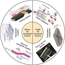
Yuexin Yin, and Daming Zhang
SignificancePhotonic integrated circuits (PICs) have been extensively researched and applied in optical interconnections, optical communication, and LiDAR. To further expand the scale and performance of photonic chips, three-dimensional (3D) PICs have emerged as a prominent research focus. 3D PICs represent an advanced type of PICs that achieve spatial expansion through coupling or three-dimensional waveguides, allowing light to propagate beyond a two-dimensional plane within the waveguide. Presently, most research and development in 3D PICs is focused on inorganic materials such as silicon, silicon nitride, and high-index silica. The preparation of 3D PICs on these material platforms necessitates polishing processes at the wafer level, which significantly increases fabrication complexity and cost. Among various optical platforms, polymer-based planar lightwave circuits stand out for their flexibility, low power consumption, and high performance. Polymers are cost-effective and can be processed using simple techniques such as spin coating and photolithography. Their fluidity allows for the creation of flat cladding without additional polishing, providing a foundation for multi-layer devices. This fluidity also simplifies hybrid integration with other material platforms. In the field of laser direct writing, many significant works have focused on waveguides based on inorganic materials. While these devices offer clear advantages in terms of propagation loss, they are limited in their capacity for modulation and reconfiguration, which impedes further functional expansion. In recent years, there has been the development of high-performance hybrid integrated photonic devices using unconventional materials such as Ⅲ-V group material, lithium niobate, and lithium tantalate, in conjunction with conventional silicon waveguides. Three-dimensional integration is regarded as the inevitable path to achieving high-performance hybrid integrated photonic devices. The polymer photonic platform presents a flexible and cost-effective alternative for developing 3D hybrid integrated chips, thus expanding future functionalities.ProgressPolymer-based 3D PICs are primarily fabricated using ultrafast laser inscription (ULI) and multi-layer stacking techniques. ULI offers precise machining and flexibility. For instance, Christian Koos’s group introduced the concept of photonic wire bonding (PWB) in 2012, enabling the connection of polymer waveguides with three-dimensional geometries to bridge nanophotonic circuits across different chips (Fig. 1). In 2018, they utilized PWB technology to connect indium phosphide (InP)-based horizontal-cavity surface-emitting lasers to passive silicon photonic circuits, achieving insertion losses as low as 0.4 dB (Fig. 2). PWB technology paves the way for hybrid photonic multi-chip assemblies that integrate known-good dies of different materials into high-performance hybrid multi-chip modules. Meanwhile, researchers at HHI have theoretically investigated and experimentally demonstrated the use of 3D PolyBoard PICs with multiple waveguide layers as a practical solution for realizing two-dimensional optical phased arrays (OPAs) with end-fire waveguides (Fig. 4). Similarly, Min-Cheol Oh’s group has developed a design and fabrication process for 3D hybrid integration OPA using silicon nitride and polymer (Figs. 13 and 14). In our group, we focus on the functional integration of polymers using 3D polymer PIC fabrication technology. We have demonstrated a dual-layer optical encryption fluorescent polymer waveguide chip based on optical pulse-code modulation technique (Fig. 7) and a 3D optical switch with thermo-optical (TO) and electro-optical (EO) tuning effects (Fig. 12). In addition, we also researched on the fabrication technology and design of hybrid integration of organic and inorganic waveguides (Figs. 9 and 10). Polymer-based 3D PICs not only provide an expandable physical dimension but also offer an optical platform compatible with a variety of materials.Conclusions and ProspectsTechniques like ultrafine laser processing, deposition, and lithography enable the preparation of complex 3D PICs. Current efforts focus on scaling up and enhancing functionalities such as phase shifters. Polymers offer potential for achieving gain amplification, optical nonlinearity, and other special properties, warranting further exploration to improve PICs’ comprehensive performance parameters. Despite their advantages, polymers face challenges like temperature and humidity sensitivity, limiting their use in extreme environments. However, progress in addressing these stability issues is ongoing. Continued research and development in polymer materials for photonic platform, particularly in 3D configurations, promise advancements not only in traditional optical communication and optical interconnect but also in quantum and space optics, leveraging processing and performance characteristics.
Aug. 10, 2024Vol. 44 Issue 15 1513004 (2024)
Jingcui Song, Zhiqiang Yang, Haiyan Shang, Lei Wan, Yan Li, Chao Lü, and Zhaohui Li
SignificanceThe world is experiencing an unprecedented information explosion. The rapid development of high-performance computing (HPC), the Internet of Things (IoT), and artificial intelligence (AI) has introduced new demands for transmission bandwidth and information capacity. However, the bottleneck of integrated circuits is gradually emerging with the slowdown of Moore’s law. Compared with traditional integrated electric circuits, photonic circuits stand out due to their unique advantages such as low power consumption, high operating speed, and multi-lane processing capability. They are regarded as a key technology in the “post-Moore era.” Photonic integrated circuits (PICs), utilizing photons as the information carrier, have emerged as a crucial technology to overcome the communication capacity crunch in modern information society. High-quality optical materials and advanced integration strategies are essential cornerstones for photonic circuits. Silicon, as a dominant semiconductor material, is a popular photonic platform owing to its large refractive index and good compatibility with the CMOS processing procedure. However, silicon exhibits a relatively high propagation loss in the communication band and strong two-photon absorption (TPA) and free-carrier absorption (FCA) effects, hindering its further applications in large-scale integrated circuits and nonlinear photonics. In recent years, a variety of alternative materials have emerged, including silicon nitride, thin film lithium niobate (TFLN), aluminum nitride, silicon carbide, and chalcogenide glasses (ChGs). Key parameters of common photonic materials are summarized in Table 1. It can be seen that the refractive index of the ChGs can be flexibly tuned over a broad range. In addition, ChGs have been extensively used in optical signal processing due to their considerable photoelastic coefficients, low propagation loss, broad transparency window, and good compatibility with various material platforms. Achieving multifunctional PICs on a single chip has become a hotspot for researchers. However, no single material can fulfill all the requirements ranging from signal generation, modulation, transmission, to detection. Therefore, heterogeneous integration is considered the optimal approach for the future evolution of integrated photonics.Progress In this paper, we review three applications of heterogeneous chalcogenide photonics based on the “ChGs+X” material platform: high-efficiency acousto-optic modulation, on-chip nonlinear parametric frequency conversion, and rare-earth ion-doped waveguide amplification (Fig. 1).1) Acousto-optical modulation: Current commercial acousto-optic modulators (AOMs) are typically made from bulk piezoelectric crystal materials like tellurium dioxide (TeO2) or lithium niobate, but their high power consumption and large volume limit their application in photonic circuits. With the rapid development of “ion cut” technology and the success of TFLN, on-chip acousto-optic modulators based on TFLN have been reported in recent years (Fig. 2). However, dry etching lithium niobate smoothly is challenging due to its chemical inertness. In addition, isolating the TFLN from the bottom SiO2 substrate is difficult due to its fragility. To address these issues, heterogenous waveguide structures are designed to achieve high-efficiency on-chip AOMs by utilizing the soft chalcogenide waveguide loaded on the low-loss TFLN. This strategy enables the creation of high-efficiency acousto-optic modulators without the need for etching or suspending the TFLN (Figs. 3-4).2) Parametric frequency conversion: The χ(2)-based nonlinear optical effect has been extensively studied. Various material platforms have been proposed to achieve efficient parametric frequency conversion, including lithium niobate, some Ⅲ-Ⅴ materials with intrinsic χ(2) nonlinearity, as well as silicon and silicon nitride with externally induced χ(2) properties. Among them, lithium niobate has been employed to achieve high-efficiency χ(2) nonlinearity by dry etching and periodical domain engineering of lithium niobate. However, this fabrication process is complex and not compatible with the CMOS procedure. Recently, bound states in the continuum (BICs) have been suggested for obtaining second harmonic generation (SHG) via modal phase matching without the need for etching the TFLN. However, the conversion efficiency is low and not suitable for wideband applications. In our work, we propose a heterogeneous integration strategy by integrating chalcogenide strip waveguide with TFLN slab (Fig. 5). This approach has enabled the realization of on-chip high-efficiency SHG and observation of broadband parametric conversion efficiency via the effect of cascaded second-harmonic generation and difference-frequency generation (cSHG-DFG).3) Optical waveguide amplification: Erbium-doped waveguide amplifiers (EDWAs) have become indispensable components in large-scale photonic circuits. To date, different material platforms and fabrication methods have been utilized to obtain efficient EDWAs such as erbium-doped Al2O3 via atomic layer deposition (ALD), erbium-doped TFLN, silicon nitride with erbium ion implantation, and rare-earth-doped chalcogenide films. However, the gain properties of ChGs-based waveguide amplifiers are lackluster for practical applications due to their intrinsically low solubility of rare-earth ions, low luminous efficiency of chalcogenide hosts, and increased etching complexity when introducing erbium ions into chalcogenide films. To address these challenges, we propose an efficient waveguide amplifier prototype without the need to dope the chalcogenide films directly (Fig. 8). The waveguide consists of a low-loss chalcogenide waveguide on a highly-doped erbium-doped Al2O3 thin film. This work facilitates the development of an efficient waveguide amplifier based on integrated chalcogenide photonics.Conclusions and ProspectsIn summary, ChGs have emerged as promising candidates in PICs. Enhancing the functionalities of ChGs by adopting integrated “chalcogenide+X” heterogeneous platforms offers valuable insights for the future development of PICs in various research fields, including optical computing, optical memory, and integrated optical engines.
Aug. 10, 2024Vol. 44 Issue 15 1513005 (2024)
Wenjun Ding, Yuting Zhang, Jing Qiu, Yongzhi Tang, Jing Zhang, Tingting Ding, Hao Li, Shijie Liu, Yuanlin Zheng, and Xianfeng Chen
ObjectiveLithium niobate based integrated photonics has been receiving extensive attention over the past decades, and its development has gained significant momentum recently thanks to the emergence of lithium niobate on insulator (LNOI). While ensuring the high performance of the device, scalable fabrication and fiber compatibility are also particularly important for practical applications. Micrometer waveguides based on 3-μm thick LNOI show excellent integration potential. For example, the lens fiber or high numerical aperture fiber can be directly coupled with the micro-waveguide with high efficiency, and the overall insertion loss of the device is small. The fabrication process of micro-waveguides by UV lithography and plasma dry etching features low fabrication cost and technical difficulty. In addition, the mode area of micro-waveguides is several times smaller than that of conventional proton-exchange or titanium indiffused waveguides, which ensures higher conversion efficiency. Here we propose to design and fabricate the LNOI micro-waveguide on 3-μm thick LNOI, demonstrating its high performance in second harmonic generation (SHG) and sum-frequency generation (SFG) at the optical telecommunication band. The excellent frequency conversion capability, scalable fabrication, and fiber compatibility make the LNOI micro-waveguide highly appealing. We expect it to form a variety of functional devices in the future and promote the development of fundamental physics research and optical quantum information applications based on integrated photonics.MethodsWe fabricate the periodically poled LNOI (PPLNOI) micro-waveguide by direct electric poling followed by UV lithography and plasma dry etching techniques. We adopt the first-order quasi-phase matching (QPM) at 1550 nm, which determines the poling period. A 3-μm z-cut magnesium-doped lithium niobate on insulator (MgO∶LNOI) wafer is patterned via ultraviolet lithography and electron beam evaporation for electrodes. The electrodes are used for direct electric poling to achieve periodic domain reversal, and PPLNOI samples are obtained. Then we use UV lithography and plasma dry etching technology to transfer the designed micro-waveguide pattern to the PPLNOI layer. During the etching process, argon ion bombardment is used, and the etching depth reaches 3 μm to completely penetrate the LNOI layer. Then, a protective layer of silica about 1 μm thick is deposited on the surface by plasma-enhanced chemical vapor deposition (PECVD). Finally, the end faces of the micro-waveguide are optically polished to obtain a buried PPLNOI micro-waveguide.Results and DiscussionsThe processes of SHG and SFG are tested to evaluate the second-order nonlinear performance of the PPLNOI micro-waveguide. The normalized SHG efficiency of the micro-waveguide is investigated under small signal approximation (1-12 mW pump). The quadratic relationship between the fundamental and the second harmonic powers is well established. The SHG conversion efficiency of the micro-waveguide is measured to be 335%/W at low pump powers. Considering the fiber coupling loss, the on-chip normalized conversion efficiency is 164%/(W·cm2). Compared with the theoretical prediction of 555%/(W·cm2), the obtained SHG normalized conversion efficiency still has a large room for improvement. As the pump power continues to increase, the quadratic relationship between them gradually degrades to linear and gradually converges to saturation. When the pump power reaches 1 W (the actual on-chip pump power is 750 mW), the second harmonic (SH) power reaches 429 mW, with an absolute on-chip conversion efficiency of 57.2%. In addition, the fiber coupling loss is only 1.2 dB/facet. The overall absolute conversion efficiency of the device is close to 30% at 1 W pump light input and remains stable over one hour. The device can maintain stable frequency conversion under watt-scale power, which shows the great potential of MgO∶PPLNOI micro-waveguide for realistic applications. Our PPLNOI waveguide also has excellent performance in the SFG process. Under 5-mW signal light, the conversion efficiency saturates when the input pumping exceeds 220 mW, and the absolute conversion efficiency is up to 139% in our experiment. This corresponds to the up-conversion of about 70% of the signal photons. The PPLNOI micro-waveguide has the advantages of low insertion loss, high scalability, and high performance. Its efficient frequency conversion provides a new choice for infrared light detection.ConclusionsWe demonstrate the fabrication process of PPLNOI micro-waveguides by UV lithography and dry etching on a 3-μm thick LNOI platform. Results show that the micro-waveguide exhibits an SHG conversion efficiency of 335%/W at low powers and an absolute conversion efficiency of 57% under 1 W pump power. When the pump power reaches 300 mW, the absolute SFG conversion efficiency of the signal light reaches 139%, achieving efficient frequency up-conversion. Our micro-waveguide is well compatible with optical fiber, featuring low insertion loss and better overall performance. It not only balances the normalized efficiency, coupling efficiency, and device length but also achieves highly efficient absolute frequency conversion at high power input, which makes LNOI micro-waveguides highly attractive for practical applications and advancing other areas of nonlinear optics.
Aug. 10, 2024Vol. 44 Issue 15 1513006 (2024)
Yongheng Jiang, Xingfeng Li, Jian Shen, Huifu Xiao, Mingrui Yuan, Pu Zhang, Yingtao Li, Yong Zhang, Yikai Su, and Yonghui Tian
ObjectiveLithium niobate on insulator (LNOI) has emerged as a promising integrated photonic platform for on-chip optical interconnection and optical communications, which is due to its outstanding characteristics, such as excellent electro-optic properties and strong optical nonlinearity. Diverse important active photonic circuit components have been proposed, including electro-optic modulators and wavelength converters. In particular, the electro-optic bandwidth of the LNOI modulator has reached up to 100 GHz and beyond, thus improving the data capacity of optical links significantly. However, with the continuous data capacity growth, the modulation rate of a single modulator will be challenging to meet the application demands. Therefore, developing a series of advanced optical multiplexers is necessary to further improve the data capacity. Recently, some advanced optical (de)multiplexing technologies have been intensively studied and reported in the LNOI platform, such as wavelength division multiplexing, polarization division multiplexing, and mode division multiplexing. Multidimensional hybrid multiplexing technologies are more important for further improving the data capacity of optical links. Among them, the dual-polarization mode (de)multiplexer (MMUX) has become a promising device as it can achieve multichannel multiplexing by only employing a single-wavelength laser, which thus lessens the cost and power consumption of optical links. However, challenges remain in realizing dual-polarization MMUX in the LNOI platform compared with the silicon-on-insulator (SOI) platform. Specifically, mode hybridization will occur in special width waveguides due to the vertical asymmetry and material anisotropy of the LNOI platform, which will introduce a lot of mode crosstalk in the bus waveguide. Therefore, we propose and demonstrate a dual-polarization MMUX with six data channels in the LNOI platform, with a subwavelength-grating taper adopted to engineer the dispersion of different modes to suppress the mode hybridization.MethodsWe employ the finite element analysis method and 3D finite-difference time-domain (3D-FDTD) method. First, we calculate the effective refractive indices of different modes in the straight waveguide as a function of the width of the waveguide (Fig. 2). The results show that the mode hybridization occurs at some specific waveguide widths when the light propagates along with the Y direction, which will introduce inter-mode crosstalk when the waveguide width changes gradually. Then, we adopt the SWG taper waveguide to suppress the mode hybridization. To design the SWG taper waveguide, we input a 1550 nm light with TM0 and TE0 mode to the left of the taper waveguide, and simulate the insertion loss and crosstalk of TM0 and TE0 mode channel as a function of the length of the SWG taper and ordinary taper waveguides respectively by the 3D-FDTD method (Fig. 5). Meanwhile, we select the 3D-FDTD simulation method to optimize the width of different taper waveguides and the coupling length of different mode coupling regions (Fig. 7).Results and DiscussionsAs proof of the concept, we fabricate a pair of dual-polarization MMUX and employ 12 TE-polarization grating couplers to interface the waveguides to optical fibers (Fig. 8). Then, an amplified spontaneous emission (ASE) and optical spectrum analyzer (OSA) are utilized to characterize the static performance of the fabricated device. The measured transmission spectra of different optical links are normalized by the PSRs with the same parameters, which are fabricated close to the device. The insertion losses of TE0, TM0, TE1, TM1, TE2, and TM2 mode channels are below 1.7 dB, 1.4 dB, 1.7 dB, 2.8 dB, 2.5 dB, and 3.1 dB respectively, while the crosstalk of TE0, TM0, TE1, TM1, TE2, and TM2 mode channels are below -10.5 dB, -17.3 dB, -10.9 dB, -11.6 dB, -10.1 dB, and -12.0 dB respectively, within the wavelength range of 1525-1565 nm (Fig. 9). Finally, the dynamic data transmission experiment with a total capacity of 1.52 Tbit/s net data rate has also been conducted (Fig. 10). To the best of our knowledge, this is the first experimental demonstration of dual-polarization MMUX with six mode channels in the LNOI platform. The proposed device has a huge potential in applications of high-speed and large-capacity optical interconnection. Thus, it has the potential to be followed by many researchers and will be applied to a large number of relevant investigations.ConclusionsIn summary, we propose, design, and demonstrate a dual-polarization MMUX with six mode channels based on the LNOI hybrid platform. The SWG taper waveguide is adopted to suppress the mode hybridization along the Y direction of the LNOI platform. The measured insertion loss and crosstalk of the fabricated device are lower than 3.1 dB and -10.1 dB respectively, within the wavelength range of 1525-1565 nm. Additionally, a high-speed data transmission experiment with a net data rate of 1.52 Tbit/s is demonstrated. Meanwhile, the fabricated device can be combined well with wavelength division multiplexing technology to realize a huge data transmission capacity. The results show that the fabricated dual-polarization MMUX has sound static and high-speed data transmission performance, which can be expected to be employed as the key to future high-speed and large-capacity optical interconnection.
Aug. 10, 2024Vol. 44 Issue 15 1513007 (2024)
Zhipeng Liu, Zhi Liu, and Buwen Cheng
SignificanceWith the exponential growth in data transmission, optical interconnection technology has replaced traditional electrical interconnection technology and become the mainstream for low-loss and high-speed transmission over medium and long distances. By utilizing photons for data transfer, optical interconnections offer significant advantages such as large bandwidth and low latency, which are crucial in meeting the demands of modern communication systems. The photodetector, which converts optical signals into electrical signals, is the core component of optical interconnection systems. Rapid advancements in telecommunications and data processing necessitate photodetectors with exceptional speed and efficiency. Among photodetectors, waveguide-coupled designs have garnered significant attention due to their compact size, high bandwidth, and easy integration with other optoelectronic devices. These attributes are critical for the development of integrated photonic circuits, which are essential for applications in data centers, telecommunications, and emerging fields such as quantum computing. Traditional high-performance InGaAs photodetectors have long been the standard in near-infrared communications. Meanwhile, Ge/Si photodetectors are rapidly advancing due to silicon photonics, which enables large-scale, low-cost production compatible with existing semiconductor manufacturing processes. The need for higher data rates and lower power consumption drives the transition from electrical to optical interconnections in communication networks. Photodetectors are crucial in this transition because they directly impact the overall performance of optical communication systems. The integration of photodetectors with waveguides not only enhances the bandwidth but also allows for the development of more compact and efficient photonic devices. This integration is essential for the continued advancement of optical interconnection technologies, expected to play a dominant role in future communication infrastructures.ProgressWe first introduce the mainstream choices for high-speed photodetectors, primarily including InGaAs photodetectors and Ge/Si photodetectors. Then we discuss the typical structures and research advancements of these two major types of photodetectors. The preferred structure for InGaAs photodetectors is the uni-traveling-carrier (UTC) structure, addressing the slow hole transport issue in III-V materials compared to the PIN structure. For example, the research group led by Seeds A J at University College London reported a high-speed evanescently coupled photodetector with a 3 dB bandwidth of 110 GHz. Li et al. from the University of Virginia reported a high-speed waveguide-coupled photodetector with a bandwidth exceeding 105 GHz, fabricated using MOCVD on an InP substrate (Fig. 1). Additionally, heterogeneous integrations of III-V photodetectors on silicon, primarily through direct epitaxy and wafer bonding, have received widespread attention. Sun et al. fabricated an improved single-carrier (MUTC) III-V photodetector on a Si substrate, achieving a responsivity of 0.78 A/W and a 3 dB bandwidth of 28 GHz under a reverse bias voltage of 3 V (Fig. 2). For silicon-based group IV photodetectors, they mainly include all-silicon photodetectors and germanium-silicon photodetectors. Researchers have achieved all-silicon photodetectors by introducing new absorption mechanisms or device structures. Intel reported a waveguide-coupled all-Si photodetector with a 3 dB bandwidth of 15 GHz (Fig. 3), achieving a responsivity of 1.6 A/W at a reverse bias voltage of 5.93 V with an active region length of 300 μm. Germanium, similar to silicon, is highly compatible with Si CMOS processes. With advancements in silicon photonics technology, waveguide-coupled Ge/Si photodetectors have become the most widely researched Si-based group IV photodetectors due to their excellent high-speed performance and mature process flow. Lischke S et al. proposed a lateral Ge/Si photodetector with a 3 dB bandwidth up to 265 GHz by reducing the width of the fin-shaped Ge absorption region (Fig. 6), marking the highest bandwidth achieved for Ge/Si photodetectors to date. The width of the fin-shaped Ge absorption region is only 100 nm, effectively reducing carrier transit time and enhancing the high-speed performance of the Ge photodetector.Conclusions and ProspectsPhotodetectors, as the core components of optical receivers, have gradually matured over the years. Our study introduces the current development of two types of waveguide-coupled photodetectors, including III-V and IV group photodetectors, each with its advantages and characteristics. Benefiting from III-V materials’ superior light absorption and high electron mobility, InP-based InGaAs photodetectors can achieve ultra-high-speed light detection based on the UTC structure, becoming the most mature photodetectors. On the other hand, IV group photodetectors, primarily Ge/Si photodetectors, are compatible with Si CMOS processes and possess inherent advantages in integration. With advanced processing technologies on silicon photonics platforms, higher processing accuracy and integration can be achieved. These features enable the fabrication of finer device structures and make ultra-high-speed Ge/Si photodetectors comparable to InP-based high-speed photodetectors. The future development of high-speed photodetectors still faces several challenges. Although Ge/Si and InGaAs photodetectors with a 3 dB bandwidth exceeding 200 GHz have been reported, their responsivity is not satisfactory. Balancing bandwidth improvement while maintaining good responsivity is an important research topic that may require the introduction of process-compatible new materials (high mobility and high absorption coefficient) or novel high-speed device structures. Furthermore, as devices’ bandwidth increases, the application scenarios of detectors in microwave photonics links will gradually expand. Unlike the low optical power input and high sensitivity detection in optical communications, this scenario requires high saturation power due to high-power input based on large bandwidth. However, large-bandwidth devices typically employ small-sized structures, making it challenging to produce photodetectors that are both high-speed and high-power-saturation. Therefore, further innovation in carrier extraction and heat dissipation of the devices is necessary.
Aug. 10, 2024Vol. 44 Issue 15 1513008 (2024)
Xiaojun Xie, Chao Wei, Jia Ye, Xihua Zou, Wei Pan, and Lianshan Yan
SignificanceWith the rapid advancement of the Internet of Things, Industry 4.0, and artificial intelligence, the global demand for communication capacity has grown exponentially. Looking toward the future, the industry is focused on researching and exploring the next-generation mobile communication technology (6G). 6G aims to leverage low, medium, and high-frequency spectrum resources for seamless global coverage, achieving peak data rates of Tbit/s. Photonic terahertz communication, offering advantages such as large bandwidth, low loss, and seamless integration with fiber optic networks, stands as a pivotal technology for future terahertz communications. Terahertz photodetectors play a critical role in these systems and have attracted considerable attention. In this paper, we summarize recent advancements in III-V terahertz photodetectors, germanium-silicon terahertz photodetectors, and heterogeneous integrated terahertz photodetectors within the communication band. This paper provides detailed insights into structural optimizations, advancements in fabrication technologies, and breakthroughs in achieving high bandwidth and power output for these photodetectors. By reviewing these developments, we aim to provide valuable guidance for the future development of high-speed, high-power photodetectors.ProgressPhotodetectors can be divided into two types based on the input light mode surface-incident and waveguide-incident photodetectors. From a bandwidth perspective, traditional surface-incident PIN photodetectors face a trade-off between bandwidth and responsivity. Increasing the thickness of the intrinsic absorption layer improves responsivity but also increases the transit time of photogenerated carriers, resulting in reduced bandwidth. Thus, bandwidth and responsivity are mutually limiting and difficult to balance. To achieve terahertz bandwidth, the thickness of the absorption layer is typically reduced, which decreases the transit time and reduces the device geometry to create terahertz photodetectors. However, the inherent bandwidth-responsivity trade-off limits further improvement in the device’s bandwidth-efficiency product. In contrast, waveguide-incident photodetectors overcome this inherent trade-off by decoupling the optical absorption process from the carrier transport process. The surface-incident III-V PIN photodetector achieves a bandwidth of 110 GHz and a bandwidth-efficiency product of 35 GHz. The latest waveguide germanium-silicon PIN photodetector achieves a bandwidth of 240 GHz and a bandwidth-efficiency product of 86.5 GHz, with a maximum bandwidth of 265 GHz (Fig. 15). From a power perspective, under high optical power conditions, photogenerated electron-hole pairs accumulate in the depletion region or at the heterogeneous interface, forming space charges. This reduces the electric field strength in the depletion region, causing the electric field to collapse, reducing the carrier drift velocity, and ultimately leading to a significant reduction in device bandwidth, responsivity, and output power. Compared to surface-incident photodetectors, waveguide-incident photodetectors experience severe local space charge effects that significantly limit their saturated output power. Traditional PIN photodetectors are limited by the slow drift velocity of the holes and strong space charge effects, which limit the output power of the device. To mitigate the space charge effect, a uni-traveling-carrier photodetector has been proposed. In this structure, the optical absorption process is decoupled from the carrier drift process by P-type doping of the absorption layer. Photogenerated holes in the P-type doped absorption layer are collected by the P-electrode through relaxation oscillation, while photogenerated electrons move to the collection layer by diffusion and are then collected by the N-electrode. In this process, only photogenerated electrons drift as effective carriers. This structure decouples the optical absorption process from the photogenerated electron transport process. Since the electron drift speed is much higher than that of holes, this structure effectively reduces the device transit time. At the same time, space charges in the depletion region can be quickly transported to the electrodes, effectively suppressing the space charge effect. On this basis, III-V uni-traveling-carrier photodetectors have achieved excellent performance by optimizing the epitaxial layer structure. The surface-incident uni-traveling-carrier photodetector achieves a bandwidth of 330 GHz, and provides an output power of -3.2 dBm@320 GHz (Fig. 12). The waveguide uni-traveling-carrier photodetector achieves a bandwidth of 220 GHz, with an output power of -1.69 dBm@215 GHz (Fig. 10). As system functions become richer and performance indicators improve, the demand for device integration increases. Therefore, integrated terahertz photodetectors and multifunctional integrated chips based on terahertz photodetectors are important research directions in photonic terahertz communication. By integrating high-performance photodetection, photonic terahertz signal processing, and high-performance terahertz signal generation functions into a single chip, system cost and power consumption would be greatly reduced, and system performance is improved. Integrated photodetectors with bandwidths of 70, 155, and 110 GHz have been implemented on SOI, silicon nitride, and thin-film lithium niobate platforms, respectively (Table 1).Conclusions and ProspectsThe terahertz photodetector is a core device in terahertz optical communication systems. We summarize the recent progress in III-V terahertz photodetectors, germanium-silicon terahertz photodetectors, and heterogeneous integrated terahertz photodetectors. III-V materials with high electron mobility are widely used in the fabrication of terahertz photodetectors. At present, terahertz photodetector devices are relatively small in size and are usually fabricated by electron beam lithography. This method is highly precise and capable of producing ultra-small devices, but it is difficult to scale up for mass production. Therefore, it is necessary to develop stepper exposure methods based on ultraviolet/deep ultraviolet lithography to fabricate large-scale, high-yield terahertz photodetector chips. For germanium-silicon photodetectors, a terahertz bandwidth germanium-silicon photodetector has been realized using custom technology. The bandwidth of germanium-silicon photodetectors based on general processes has reached 103 GHz (Table 1). The device bandwidth is expected to be further improved by optimizing the device structure and electrode configuration. Heterogeneous integrated photodetectors based on wafer bonding or epitaxial growth have demonstrated 100 GHz bandwidth. The next step is to achieve ultra-large bandwidth and multi-function integration of heterogeneous integrated chips. This will meet the bandwidth, output power, responsivity, and integration requirements of photonic terahertz communication systems.
Aug. 10, 2024Vol. 44 Issue 15 1513009 (2024)
Ruijun Wang, Yu Han, and Siyuan Yu
SignificanceSilicon is an indirect bandgap semiconductor that cannot emit light efficiently. In contrast, Ⅲ-V compound semiconductors such as AlGaAs/GaAs and InGaAsP/InGaAlAs/InP are direct bandgap semiconductors widely used for fabricating efficient electrically driven laser devices. As silicon-based photonic integrated circuits enter commercial application, integrating Ⅲ-V compound semiconductor lasers on silicon has become a key bottleneck for its future development.ProgressThree main kinds of approaches have been developed aimed at integrating Ⅲ-V semiconductor laser sources on silicon photonic chips. The hybrid integration approach mounts prefabricated semiconductor laser chipsets on silicon photonics substrates by means of precision flip-chip bonding between gold pads. To achieve high optical coupling efficiency between the laser chipset and the silicon waveguide, the main technical challenges include repeatable sub-micron three-dimensional alignment and optical mode matching. Precision alignment mainly relies on high-precision equipment in the horizontal direction and carefully designed mechanical structures in the vertical direction, while optical mode matching relies on predesigned mode converters. This technology has been put into small-volume production but faces challenges in terms of productivity, yield, and cost. The heterogeneous integration approach is based on transferring Ⅲ-V active devices or films onto silicon by means of transfer printing or die-to-wafer bonding. In transfer printing, prepared Ⅲ-V lasers are picked up by an elastomer stamp and attached to a silicon substrate by van der Waals force or by an adhesion agent. Compared with flip-chip bonding, transfer printing is a flexible process that can integrate multiple devices of different kinds in one step. Optical coupling with the underlying silicon waveguide is usually achieved via evanescent coupling. In die-to-wafer bonding, Ⅲ-V epitaxial wafers are diced into desired sizes and placed with their active side up on a carrier plate by temporary bonding. The carrier plate with the dies is then activated in plasma and flipped over to bond the dies to the silicon photonics wafer. The carrier plate is then removed, and the Ⅲ-V dies are thinned to remove their original Ⅲ-V substrate, leaving only the active epi-layer attached to the silicon wafer. Semiconductor lasers are then fabricated in the active epi-layer, precisely aligned to the underlining silicon waveguide by means of photolithography alignment markers to ensure high-efficiency evanescent coupling. This technology has successfully realized wafer-scale production. While promoting productivity, the yield of both transfer printing and die-to-wafer bonding approaches is still being improved. The direct epitaxy of Ⅲ-V semiconductors on silicon is attractive as a truly wafer-scale production approach but faces significant challenges in terms of crystal lattice mismatch, thermal mismatch, and anti-phase domains at the epi-interface which leads to high stress and high defect densities in the Ⅲ-V epi-layer. Various schemes have been developed, including blanket growth and selective area growth. In blanket growth, thick buffer layers are needed to reduce the defect density in the Ⅲ-V active layer, which can prevent optical coupling between the Ⅲ-V active layer and the underlying silicon waveguide. Growth in etched pits can align the active layer with the silicon waveguide but faces problems in laser facet quality. Using quantum dots instead of bulk or quantum well active layers significantly mitigates adverse effects of defects on laser efficiency and lifetime. Vertical selective area growth can produce high-quality Ⅲ-V crystals by means of defect-trapping, but micro-sized material cannot support electrodes for current injection. Horizontal selective area growth enables epi-growth of Ⅲ-V materials and quantum-well active structures in the lateral direction, forming larger-sized Ⅲ-V films co-planar with the silicon waveguide layer, therefore demonstrating promising potentials for electrically pumped semiconductor lasers efficiently butt-coupled with the silicon passive waveguide.ConclusionsⅢ-V lasers on silicon photonics chips have been realized through hybrid integration, heterogeneous integration (including transfer printing and die-to-wafer bonding), and direct epitaxy. While hybrid and die-to-wafer bonding approaches have been commercialized in small to medium-volume production, further improvement in terms of their productivity and yield is needed. The direct epitaxy approach as a true wafer-scale remains an attractive long-term solution requiring substantial research and development.
Aug. 10, 2024Vol. 44 Issue 15 1513010 (2024)
Junling Qu, Peng Liu, Xuetao Gan, and Jianlin Zhao
SignificanceSilicon photonics combines the high speed and broad bandwidth of optical signals with high-density and low-cost fabrication of the complementary metal oxide semiconductor (CMOS) technology, and it has been an attractive technology for various applications ranging from data centers to biosensing. However, silicon is not capable of building several active optoelectronic devices for fully integrated photonic circuits. For example, the indirect bandgap of silicon makes it challenging to achieve efficient light sources, the absence of the Pockels effect prevents silicon from building high-speed linear electro-optic modulators, and the absorption cutoff wavelength of 1100 nm makes silicon incompatible with telecom-band photodetection. A common strategy to overcome such limitations is the heterogenous/hybrid integration of material technology suitable for active optoelectronic devices, such as the epitaxy growth of germanium for telecom-band photodetectors and wafer-bonding of III-V semiconductors for on-chip lasers and modulators. However, such integration has problems including the lattice mismatch during epitaxy, high cost, low yield of bonding, and optical mode mismatch between different materials. Therefore, it is necessary to develop novel material platforms that can provide high-performance active devices with CMOS-compatible fabrication. In this regard, colloidal quantum dot (CQD) semiconductors featuring excellent optoelectronic properties, low-cost chemical synthesis, and CMOS-compatible solution-based fabrication emerge as a competitive material platform for active devices integrated into silicon photonic chips. Due to their continuously tunable bandgap from UV to THz enabled by the quantum confinement effect, near-unity photoluminescence quantum yield, narrow emission linewidth, and highly tunable carrier transport, the potential applications of the CQD have been demonstrated by the commercialization of CQD-enhanced liquid crystal display by Samsung company and the short-wave infrared camera of SWIR Vision Systems company. Meanwhile, their applications in light-emitting diode display, solar cells, and quantum emitters are extensively researched. In this respect, the 2023 Noble Prize in Chemistry was awarded to Alexei Ekimov, Louis Brus, and Moungi Bawendi for the discovery and development of CQDs. Over the last decade, there have been several studies on CQD active devices integrated into silicon photonic chips, including waveguide-integrated photodetectors, light-emitting diodes, and optically pumped lasers. Thus, it is necessary to provide readers of different academic backgrounds with a full picture of CQD materials, including their synthesis route, thin film fabrication, and optoelectronic properties related to the chip-integrated active devices. Additionally, it is high time to update the latest progress in chip-integrated CQD active devices and discuss the possible route for their future development.ProgressFirst, the colloidal synthesis of CQDs and their solution-based thin film deposition are introduced, with an emphasis on the role of surface organic ligands in governing the solution stability and controlling the optoelectronic properties of CQDs. The optical properties of CQDs related to their integration on silicon photonic chips are then summarized. Specifically, their spectral coverage from UV to THz range is achieved by quantum confinement effect and heterostructure band alignment, and their complex refractive index can be tuned from 1.7 to 2.7 by the CQDs material composition, surface ligand and film deposition strategy (Table 1). Meanwhile, the optical gain characteristics (gain magnitude, gain threshold, and gain lifetime) and their measurement methods (transient absorption and variable stripe length methods) are presented, with the optical gain properties of the most employed CQDs summarized in Table 2. Regarding the electrical properties of CQDs, we introduce ligand exchange processes that provide conductive CQD thin films with by-design doping types and magnitude, which is the core of fabricating high-performance active optoelectronic devices. After introducing the fundamental optoelectrical properties of CQDs, we present the fabrication level and summarize the patterning strategies of CQD thin films including lithography, ink-jet printing, 3D printing writing, and transfer printing, thus demonstrating the feasibility of CQD-based active device integration with silicon. In the next section, we summarize the latest progress in chip-integrated CQD-based photodetectors and light sources. In terms of CQD-based photodetectors, plasmonic-Si hybrid waveguide integrated HgTe CQD-based photoconductor and SiN waveguide integrated PbS CQD-based photodiodes are presented. Additionally, we show their performance including the responsivity, 3 dB bandwidth, and external quantum efficiency in Table 3. Their current limited photodetection performance is attributed to factors such as high dark current from a photoconductive configuration, low carrier mobility from solid-state ligand exchange, and photocurrent saturation due to the evanescent coupling between the photodetector and the waveguide. Regarding the chip-integrated CQD-based light sources, the electrically pumped light-emitting diode has poor outcoupling efficiency of below 1% due to a lack of emission directionality. On the other hand, waveguide-coupled CQD-based lasers have attracted more research interest. We summarize the structure and performance of these lasers in Table 4 and present their developments in detail by dividing them into additive and substrative manufacturing categories. For additive manufacturing, the self-assembled supraparticle and microring resonator lasers made of CQDs are demonstrated and outcoupled by waveguides. We also present template-assisted CQD microring lasers with predefined patterns, with higher flexibility and controllability shown. Plasmonic waveguide integrated CQD lasers are also developed to demonstrate coherent output sources at sub-diffractive scale. Meanwhile, with a fully CMOS compatible fabrication process, subtractive manufacturing of a sandwich-structured SiN/CQD/SiN thin film has been developed by the van Thourhout group from Gent University, with successful demonstrations of low-threshold picosecond laser pumped micro-disk lasers and quasi-continuous-wave pumped diffracted feedback lasers.Conclusions and ProspectsWith the advances in synthesis, device physics, and CMOS compatible thin film fabrication of CQDs, their integration with silicon photonic chips is drawing increasing attention. We expect that the advantages of CQDs can be better leveraged in the direction of long-wavelength infrared photodetectors, and more interestingly, the electrically pumped on-chip lasers that are in high demand in current silicon-based optoelectronic technology. The development of electrically pumped on-chip CQD lasers will rely on the invention of novel CQD materials with better optical gain properties, the rational design of electrical and optical structures, and their extension to infrared wavelength.
Aug. 10, 2024Vol. 44 Issue 15 1513011 (2024)
Zifeng Chen, Zhida Wang, Jiajun Lou, Quanan Chen, Chun Jiang, Juan Xia, Qiaoyin Lu, and Weihua Guo
ObjectiveA tunable laser is one of the crucial technologies in optical networks due to its advantage of flexibly switching output wavelengths. After years of research, tunable semiconductor lasers have developed various solutions. Super-structure grating distributed Bragg reflector (SSGDBR) tunable lasers, modulated grating Y-branch distributed Bragg reflector (MGY-DBR) lasers, and chirped sample grating distributed reflector (CSGDR) tunable lasers can achieve wide-range tuning. External cavity lasers (ECL), distributed feedback (DFB) lasers, and vertical cavity surface emitting lasers (VCSELs) are typical structures used for tunable lasers. The cavity length of ECL can be very long, resulting in a very narrow linewidth. However, its large volume makes it difficult to integrate with other devices on a single chip. The tuning range of a single DFB laser is only 3-5 nm, which cannot meet the requirements for wide-range tuning. To achieve wide-range tuning, multiple DFB lasers with different center wavelengths can be integrated into a DFB array. Although the manufacturing process of DFB lasers is mature, ensuring the integration of multiple lasers on the same chip remains challenging. VCSELs have a short cavity length and high reflectivity, resulting in a large longitudinal mode spacing and good single longitudinal mode performance. However, they exhibit multiple transverse modes and a larger linewidth, which makes integration with other devices challenging. To address the limitations of the aforementioned lasers, we design and propose a monolithic integrated tunable laser-multi-channel interference (MCI) laser. This laser achieves wavelength tuning based on the thermal optical effect by selecting modes through arm interference of different lengths. Unlike the lasers mentioned earlier, the MCI laser does not require a grating for mode selection. Additionally, each arm can independently change the phase and control the laser wavelength, significantly simplifying the laser production process and increasing production tolerance. Through multiple rounds of design and iteration, our study has successfully verified the feasibility of the scheme and achieved transmitter optical subassembly (TOSA) packaging and miniaturized integrated components for this laser.MethodsMCI laser includes an active section for optical gain, a semiconductor optical amplifier (SOA) section for amplifying output optical power, and a multi-channel interference region for mode selection. The multi-channel interference section is composed of a common phase section for tuning longitudinal modes and a 1×8 multi-mode interferometer (MMI) for beam splitting, with 8 arms of different lengths. Each arm end is equipped with a multimode interference reflector (MIR) that reflects the total light to the active section, and a metal thermal electrode is positioned above each arm. The 8 arms independently adjust the phase of the light field based on the thermal optical effect, enabling interference to obtain a reflection spectrum dominated by a single reflection peak. Adjusting the phase interference of the 8 arms enhances coarse wavelength adjustment while adjusting the longitudinal mode of the common phase zone facilitates fine wavelength adjustment. The shape of the entire reflection spectrum can be optimized by adjusting the differences in arm lengths. Optimizing these differences is crucial for achieving better single-mode performance of MCI lasers. During the optimization of arm length differences, it is essential to consider suppressing adjacent longitudinal modes and other modes far from the main reflection peak simultaneously. We propose a method using particle swarm optimization (PSO). The PSO algorithm is combined with the multi-mode rate equation to optimize the laser arm lengths and obtain the optimal arm length design method, thereby achieving a better reflection spectrum across the entire wavelength band. The signal-to-mode suppression ratio (SMSR) of the wavelength at 1515 nm, at the edge of the gain spectrum, serves as the optimization index for the PSO algorithm, ensuring it exceeds 45 dB across the entire band and controls the half-width of the main peak to suppress adjacent longitudinal modes. After iterative analysis, a set of eight arm lengths is determined: 140.00, 268.28, 384.64, 521.80, 526.80, 674.00, 681.25, and 750.41 μm.Results and DiscussionsThe MCI laser achieves a tuning range of 48 nm covering the C++ band (1524-1572 nm). It boasts an SMSR exceeding 46 dB and a fiber-coupled output power exceeding 16.5 dBm. Both SMSR and output power depend on the gain of the active region. The peak of the gain spectrum maximizes gain, minimizes threshold current, maximizes SMSR, and optimizes output power. Moving away from this peak increases threshold current, reducing SMSR and output power accordingly. The gain spectrum steepens towards shorter wavelengths, accelerating reductions in SMSR and output power in that direction. Frequency deviation from the international telecommunication union (ITU) standard remains within ±0.5 GHz across all channels and is wavelength-independent. Further optimization can be achieved by adjusting the TEC1 operating temperature. Wavelength drift is less than ±1 pm, demonstrating excellent temperature control and wavelength locking performance. Output optical power for 120 wavelengths remains fixed within different values (12-16 dBm), and the power deviation is maintained within ±0.1 dB. The reverse bias extinction ratio (ER) in the SOA region exceeds 40 dB, and all wavelength channels achieve a narrow linewidth of less than 150 kHz. The ITLA’s total power consumption is less than 3 W under 75 ℃ environment.ConclusionsA new type of monolithic wide-range tunable semiconductor laser—MCI laser, is proposed. This device utilizes thermal-optical effects and 8-arm interference enhancement to adjust reflection peaks and longitudinal modes, achieving wavelength tuning akin to a distributed Bragg reflector (DBR). With the absence of grating structures, it offers advantages in fabrication simplicity and tolerance. The integration of offset quantum wells technology for active and passive components reduces regrowth complexity. The MCI laser features a wavelength tuning range exceeding 48 nm, SMSRs greater than 46 dB, Lorentzian linewidths less than 150 kHz, and consumes less than 50 mW for total thermal tuning power. The MCI laser chip, thermoelectric cooler (TEC), and wavelength locking device are packaged into a TOSA box, achieving an integrated tunable laser assembly (Nano-ITLA) measuring only 25.0 mm×15.6 mm×6.5 mm. Fiber-coupled output powers exceed 16.5 dBm, covering 120 ITU channels with frequency deviations less than ±0.5 GHz in the C++ band. Under wavelength locking and power balancing control, wavelength drifts are less than ±1 pm, power jitters are less than ±0.1 dB, and the reverse-biased SOA section exhibits extinction ratios greater than 40 dB. The MCI wide-range tunable laser demonstrates excellent potential for applications in coherent optical communication.
Aug. 10, 2024Vol. 44 Issue 15 1513012 (2024)
Mengwei Sheng, Wei Wang, Jinlong Xiao, Yuede Yang, and Yongzhen Huang
ObjectiveNarrow linewidth semiconductor lasers are crucial in coherent optical communications due to their low phase noise. The rapid growth in network capacity demands advanced modulation formats with stringent phase stability requirements, necessitating lasers with linewidths of 100 kHz or lower. The square Fabry-Perot (FP) coupled cavity consists of a square microcavity and an FP cavity directly connected. The FP cavity acts as the main gain component, while the square microcavity serves as the selective reflective end facet. The strong coupling between the whispering gallery mode and the FP mode achieves a high side-mode rejection ratio and efficient coupling output, though the laser linewidth is typically in the MHz range. We aim to drastically narrow the linewidth of the square FP coupled-cavity laser for coherent optical communications.MethodsUsing the finite element method, we simulate the reflectance of an 18 μm side-length square microcavity, identifying seven transverse modes with reflectance greater than 0.7 within twice the longitudinal mode spacing. We also simulate the mode characteristics of a coupled cavity with an FP cavity length of 550 μm and a width of 2 μm. Analyzing the square cavity reflectance, coupled-mode Q-factor, and the fundamental transverse mode proportion in the FP cavity, we determine that the coupled mode corresponding to the sixth-order whispering gallery mode is preferentially excited in the actual device. Subsequently, we fabricate square FP coupled-cavity lasers using a 3 quantum-well AlGaInAs/InP epitaxial wafer with dimensions of side length a=18 μm, FP cavity width w=2 μm, and length L=550 μm. The deeply etched laser waveguide’s optical confinement factor is approximately 0.34%, effectively reducing the Lorentzian linewidths.Results and DiscussionsWe measure the single-mode fiber-coupled output power and voltage characteristics of the square FP coupled-cavity laser, finding a resistance of about 7 Ω and a single-mode fiber-coupled output power of 13 mW. The main mode is at 1550.5 nm with a side-mode suppression ratio of 47 dB for injection currents ISQ=35 mA and IFP=165 mA. The spectrum’s envelope aligns with the square microcavity’s reflectance spectrum. With a fixed square microcavity injection current ISQ=18 mA, we observe the lasing spectrum variation with the FP cavity injection current IFP. Below the threshold current, the fundamental mode of the square microcavity at 1519.2 nm is visible. As IFPincreases, the coupled mode lases at about 1521 nm, separated from the fundamental whispering gallery mode by 1.6 nm. The anti-symmetric fundamental mode in the square microcavity, having the highest Q-factor, is preferentially excited. The lasing mode forms by coupling the sixth-order whispering gallery mode with the FP mode. Near IFP=70 mA, the lasing mode hops from 1521 nm to 1548 nm, corresponding to twice the longitudinal mode spacing of the square microcavity. We measure the frequency noise power spectral density of this laser using the self-homodyne optical coherent receiver method and obtain a Lorentzian linewidth as low as 233 kHz, maintaining around 300 kHz with stable single mode lasing.ConclusionsWe design a narrow linewidth square FP coupled-cavity laser with a 3 quantum-well AlGaInAs/InP epitaxial wafer and a low transverse optical confinement factor. The square microcavity has a side length of 18 μm, and the FP cavity measures 2 μm in width and 550 μm in length. Simulations and experiments indicate that the coupling mode corresponding to the higher-order whispering gallery mode of the square microcavity is excited. The laser’s maximum single-mode fiber-coupled output power is 13 mW, with a maximum side-mode suppression ratio of 47 dB, and a Lorentzian linewidth of 233 kHz.
Aug. 10, 2024Vol. 44 Issue 15 1513013 (2024)
Shujun Liu, Ruoran Liu, Xiaowan Shen, Lijia Song, Dajian Liu, Xiaolin Yi, Weike Zhao, Shihan Hong, Long Zhang, and Daoxin Dai
SignificanceMultimode photonics has become increasingly attractive globally in recent years due to its potential for achieving ultra-high-performance on-chip photonic devices and large-scale photonic integration. This potential is realized through the introduction of broadened optical waveguides and the controlled manipulation of their fundamental and higher-order modes. Without necessitating changes to the fabrication process, multimode photonics overcomes the performance bottleneck previously inherent to single-mode condition-designed photonic devices. Consequently, this field paves the way for developing high-performance photonic devices without increasing fabrication complexity. High-index-contrast multimode photonic waveguides with strong mode dispersion play a key role in multimode photonics. Successful developments in this area have shown great potential for meeting application demands. Silicon photonic waveguides are particularly advantageous due to their ultra-small cross sections, low-cost fabrication, and strong mode dispersion from their ultra-high index contrast, providing a solid fundamental for high-performance multimode photonic devices. Flexible mode manipulation has proven multimode photonics to be extremely useful, leading to three types of devices: mode-division-multiplexed photonic devices, high-order-mode-assisted photonic devices, and broadened-waveguide photonic devices.ProgressInitially, multimode photonic devices for mode-multiplexing systems offer significant benefits such as low loss, minimal crosstalk, and wide bandwidth, enabling support for multiple channels. Notable among these are multi-channel mode-division (de)multiplexing (MDM) devices, multimode waveguide bends, and crossings, demonstrating exceptional channel expansibility. Integrating MDM with wavelength-division multiplexing (WDM) and polarization-division-multiplexing establishes multi-dimensional multiplexing systems, offering promising solutions for high-capacity data transmissions. However, efficiently coupling multi-mode optical waveguides with few-mode fibers remains challenging, requiring further research to minimize coupling loss and inter-mode crosstalk. In photonic engineering, a shift towards multimode photonic waveguides beyond the conventional single-mode regime has revealed unparalleled potential. This approach has led to propagation losses and random phase errors at remarkably low levels, surpassing the limitations of traditional single-mode waveguides. Notably, this opens possibilities for key photonic components like ultra-low-loss optical delay lines, ultrahigh-Q microcavities, arrayed-waveguide gratings (AWGs) with significantly low crosstalk, and Mach-Zehnder interferometers (MZIs) with near-zero random phase errors. These advancements break existing performance ceilings, offering a promising direction for large-scale photonic integration. The advent of silicon photonic devices utilizing higher-order modes marks a new era of substantial development potential. By harnessing the transition from using only the fundamental mode to incorporating both fundamental and higher-order modes, these devices employ unique properties of higher-order modes to achieve previously unattainable feats. This includes special functional elements capable of precise polarization manipulation, adaptive dispersion control, and bandpass filtering, evidenced by efficient polarization beam splitters and rotators, dynamically tunable dispersion compensating chips, and sophisticated multi-channel photonic filters with box-like responses, underscoring the significant impact of higher-order-mode-assisted silicon photonics. As multimode photonic technologies advance, a sophisticated range of high-performance devices is emerging, playing an increasingly critical role within optical systems spanning transceivers, routing, and quantum optics. The introduction of MDM highlights the need for reconfigurable optical add-drop multiplexer (ROADM) chips capable of agile mode channel manipulation. Research in multimode photonics also ventures into quantum optic chips, transcending classical integrated photonics.Conclusions and ProspectsIn essence, breaking free from the constraints imposed by the single-mode condition unveils a plethora of innovative opportunities and intricate challenges in integrated photonics. This paradigm shifts purred the emergence of multimode photonics, already celebrated for pioneering functional implementation and performance enhancement. Breakthroughs in multimode photonics lay a cornerstone in the ongoing quest for superior photonic devices and serve as essential scaffolding for large-scale photonic integration, playing a pivotal role in advancing the field towards a new era of photonics technological advancements.
Aug. 10, 2024Vol. 44 Issue 15 1513014 (2024)
Yu Li, Qiang Li, Dapeng Liu, Junbo Feng, and Jin Guo
SignificanceThe development trend of silicon photonic integrated circuits (SiPICs) in recent years parallels the historical evolution of integrated circuits (ICs). In terms of chip integration scale, digital ICs had achieved a scale of 106 before 1990, and by 2020, they had advanced to ultra-large scale integration ranging from 1010 to 1011. Over decades, the development of digital ICs has adhered to “Moore’s Law”, where significant reductions in operating voltage due to transistor miniaturization have enhanced efficiency and integration. Smaller chip sizes allow for more chips to be produced from the same-sized wafer, thus reducing marginal costs. From the perspective of signal carrier properties, the optical carrier transmission process in SiPIC exhibits typical analog signal characteristics, akin to analog ICs that focus on processing high-frequency continuous signals. System performance emphasizes factors like signal-to-noise ratio, distortion, power consumption, and stability. In terms of integration density limits, SiPIC shares similarities with analog ICs. Unlike digital ICs, analog ICs do not always benefit from transistor miniaturization as they do not strictly follow Moore’s Law for iteration. Smaller transistor sizes can sometimes compromise the overall performance and operational stability of high-voltage power management chips. Traditionally, analog ICs have also leaned towards mixed-signal technology development. For SiPIC, the challenge lies in the optical diffraction limits that make it difficult to reduce the width of optical waveguides below 100 nm. Additionally, achieving nanoscale modulation devices faces material constraints, posing hurdles to increasing integration density. For downstream applications, there exists a significant correlation between larger SiPIC chip scales and better system performance. In optical communication transceiver modules, scaling up in parallel can increase the number of transceiver channels, thereby strengthening overall module throughput. In photon AI computing, increased parallelism allows for more channels, facilitating larger convolutional kernel computations and higher data throughput. Longer cascaded links can also support a broader range of matrix calculations, boosting data fitting capabilities. In Lidar applications, augmenting the number of phased array antennas effectively enhances beam quality and directional accuracy. Therefore, the expansion in device scale, coupled with higher signal quality requirements and limited potential for miniaturization, poses unique challenges for large-scale integration of silicon-based optoelectronic chips, distinct from those encountered in traditional digital or analog circuits.ProgressWe introduce technical solutions for the entire process of scalable design and manufacturing, along with the iterative processes between fabs and design customers. We then analyze the fundamental integrated devices in SiPIC from the perspective of on-chip large-scale device integration, including IO switching devices, transmission devices, passive control devices, active control devices, light sources, and detectors. Furthermore, we examine the theoretical limit of integration scale for silicon optoelectronic devices at the current technological level. The essence of scaling SiPIC lies in the reuse, modification, and combination of device units. Designers at the link level focus on optimizing performance, footprint, process sensitivity, and environmental robustness through rational architectural design. Using SiPIC AI and Lidar chip design as examples, we analyze common SiPIC AI design architectures and device layout methods, discuss the characteristics and limitations of waveguide routing and metal wiring in PIC chips, and explore the challenges and prospects of achieving large-scale integration of SiPIC at the circuit level. The number of components in SiPIC chips has reached the order of 104, including optical and electrical components, as well as electrical IO ports, also numbering around 104. The yield rate issue, encompassing the reliability of numerous optoelectronic components during manufacturing and their consistency within and across chips and wafers, is crucial for mass production feasibility and lowering production costs. Therefore, we analyze the manufacturing challenges of electrical and optical components in chip manufacturing from the perspective of large-scale production and discuss the development trajectory for large-scale manufacturing of SiPIC.Conclusions and ProspectsSiPIC demonstrates higher upper limits in terms of operating frequency, channel multiplexing, and anti-interference compared to traditional ICs, fostering complementary development with them. However, achieving larger scale integration and broader application support still lacks systematic automated design tool support. There remain numerous engineering challenges related to material systems, process flows, and packaging testing that need addressing to gradually reduce procurement costs and mitigate application risks for downstream demands. In the short term, increasing SiPIC integration can be achieved by reducing device sizes and optimizing device performance. Through reverse design, generative adversarial networks, and other advanced optimization algorithms, the design space can be expanded to achieve superior device performance with smaller footprints. Collaborative optimization algorithms for process flows and device design can establish processing conditions at the design stage, narrowing the performance gap between design and fabrication and strikingly improving manufacturing yield. Moreover, the introduction of new process platforms and the integration of new materials heterogeneously—such as graphene, plasmonics, and two-dimensional van der Waals heterostructures—can offer new solutions for shrinking device sizes and refining the optical and electrical properties of current devices. In the long term, due to optical diffraction limits and spot size constraints, the device integration density of SiPIC will encounter inherent limits. Future developments may parallel analog ICs, leveraging advantages in signal quality and rate to complement digital IC functions. This convergence aims to optimize system-wide power consumption, performance, and cost control.
Aug. 10, 2024Vol. 44 Issue 15 1513015 (2024)
Weijie Tang, and Tao Chu
SignificanceThe exponential growth of data driven by big data and artificial intelligence is propelling data centers towards larger scales. The adoption of decoupled architectures has increased the number of interconnection nodes and data exchanges within these centers, particularly in new data centers tailored for artificial intelligence where distributed training requires a considerable data exchange between GPU nodes. Minimizing communication-to-computation ratio is crucial for efficient distributed machine learning frameworks. Despite using low-power, high-bandwidth optical interconnections for node-to-node data transfer, signal switching in data centers still relies heavily on a hierarchical structure of electrical switches. These traditional switches, constrained by bandwidth and port count, are inadequate for escalating demands of data transmission. Future high-performance, large-scale, and green data centers are likely to rely on optical switches offering high bandwidth, low latency, and minimal power consumption. Among various optical switch technologies, silicon photonic switching stands out due to its nanosecond-scale switching time, ultra-low power consumption, high integration potential, and compatibility with CMOS fabrication processes.ProgressScholars have focused on innovating silicon photonic switches configured in a cascaded Mach-Zehnder Interferometer (MZI) setup (refer to Table 1). The phase shift arm within the MZI structure, which modulates the refractive index through different mechanisms, primarily differentiates into electro-optic (EO) switches that leverage the carrier dispersion effect and thermo-optic (TO) switches that operate on thermal effects. Scaling port integration has been a central tenet in silicon photonic switch research, with advancements such as 32×32 EO switches achieved in 2017 and 64×64 TO switches in 2018, boasting rapid link switching time of approximately 1 ns. Generally, at equivalent scales, TO switches exhibit lower loss and superior crosstalk performance, while EO switches offer faster switching speeds and lower energy consumption due to their operational principles. Challenges remain in device calibration, optoelectronic hybrid packaging, and cumulative optical path loss management with network scaling, limiting the realization of larger-scale silicon photonic switches.The development of large-scale silicon photonic switches hinges on key technologies such as network architecture optimization, unit device enhancement, loss compensation techniques, switch unit calibration, and optoelectronic hybrid packaging. These technologies are deeply interconnected and necessitate a balanced and integrated approach to achieve improvements. Network architecture forms the cornerstone for constructing large-scale optical switches, requiring comprehensive optimization that addresses switching path control, unit device calibration, and cumulative link loss. While unit device performance has nearly peaked, integrating III-V material devices to compensate for optical link losses poses technical challenges such as material integration and thermal management. Optoelectronic detectors or grating devices for monitoring and calibrating the switch unit states within integrated switch chips strain electrical packaging and raise practicality concerns in large-scale optical switch systems. System-level calibration methods hold promise but require validation for reliability. Optical and electrical packaging constraints present challenges during large-scale optical switch assembly, necessitating suitable optoelectronic hybrid packaging strategies considering network architecture, dimensions, optical coupling techniques, and control requirements.Conclusions and ProspectsThe future demand for high-performance, large-scale green data centers underscores the development trajectory for silicon photonic switches. While silicon photonic technology is highly competitive in achieving low-power, large-scale optical switching devices, current loss and crosstalk performance must be further reduced to meet data center requirements. Progress in heterogeneous integration technologies, system-level unit device calibration methods, and advanced packaging technologies is expected to resolve bottleneck issues arising from increased device integration and calibration complexities. This progression paves the way for the realization of high-performance, highly integrated, and energy-efficient optical switches capable of supporting thousands of ports.
Aug. 10, 2024Vol. 44 Issue 15 1513016 (2024)
Changhao Han, Haoyu Wang, Haowen Shu, Jun Qin, and Xingjun Wang
SignificanceThe advent of next-generation information technology has spurred rapid advancements in fields like big data, cloud computing, and artificial intelligence, resulting in an exponential increase in global data volumes. However, traditional electrical analog and digital communication techniques face limitations such as bandwidth constraints, rising power consumption, severe crosstalk, and significant transmission losses when dealing with such vast data amounts. These challenges pose significant hurdles in designing electronic chips used in communication systems. Optical communication, relying primarily on fiber-optical technology, has emerged as a critical component in data centers and ultra-long-distance signal transmission networks due to its inherent advantages: vast bandwidth, high-capacity transmission, minimal losses, and reduced crosstalk. In recent years, breakthroughs in optoelectronic integration technology have enabled the miniaturization and multifunctionality of traditional fiber-optical communication systems. This trend has catalyzed a surge in manufacturing, packaging, and IP development of chips tailored specifically for optical communication, marking a dynamic growth trajectory in this field. Silicon photonics technology aims to integrate optoelectronic devices onto a silicon platform, constructing comprehensive optoelectronic systems that enable intricate functionalities. This technology boasts numerous advantages, including an abundant supply of raw materials, compatibility with CMOS manufacturing processes, mature and highly reliable processing techniques, as well as a diverse array of functionalities for both active and passive systems. Consequently, it serves as a pivotal approach for miniaturizing and boosting the multifunctionality of optical communication systems. Silicon-based electro-optical modulators play a crucial role in converting signals between the electrical and optical domains, occupying a central position in information transmission and processing. Exploring the latest developments in silicon-based modulators and alongside analyzing structural designs, methodologies, strengths, and weaknesses of various modulator types are imperative for guiding researchers in devising devices that exhibit superior performance and align better with practical application requirements. Therefore, conducting a comprehensive review and analysis of existing research on silicon-based modulators is necessary and holds great importance.ProgressSilicon-based modulators are generally classified into two categories: pure silicon modulators and silicon-based heterogeneous integration modulators. Among pure silicon modulators, we specifically discuss the silicon Mach-Zehnder modulator (MZM), silicon microring modulator (MRM), and silicon slow-light modulator. Firstly, we delve into the working principles and historical evolution of silicon MZMs, providing a thorough analysis of different structural designs and key performance metrics (Figs. 1-3). Currently, segmented MZMs utilizing lateral PN junction structures have achieved an impressive electro-optical bandwidth of 67 GHz, and a modulation efficiency of 3 V·cm. Nevertheless, the relatively large size of MZMs remains a challenge for integration. In contrast, silicon MRMs offer a more compact footprint and leverage a lumped electrode for wider bandwidths. Presently, MRMs have demonstrated electro-optical bandwidths surpassing 67 GHz and a modulation efficiency of 0.52 V·cm (Figs. 4 and 5). Nonetheless, silicon MRMs are notably susceptible to environmental disturbances and process variations, which hinder their practical deployment. On the other hand, silicon slow-light modulators exploit the slow-light effect to enhance modulation efficiency. Compared to MZMs, they achieve higher efficiency with a smaller form factor, boasting a large passband and superior thermal stability over MRMs. These modulators have achieved electro-optical bandwidths exceeding 110 GHz on a scale of hundred micrometers (Fig. 8), underscoring their promising potential for future advancements. For silicon-based heterogeneous integration modulators, we provide an analysis and summary encompassing four categories: silicon-based germanium modulators, silicon-based polymer hybrid modulators, silicon-based lithium niobate thin-film modulators, and silicon-based two-dimensional material modulators. Silicon-based germanium modulators incorporate germanium material onto a silicon substrate, utilizing the electro-absorption effect for modulation. These modulators have achieved an electro-optical bandwidth of 110 GHz with a modulation arm length of 20 μm (Fig. 9). Silicon-based polymer hybrid modulators exploit the Pockels effect, enabling the fabrication of microring modulators with an electro-optical bandwidth of up to 176 GHz. Furthermore, these modulators exhibit excellent thermal stability (Fig. 10). Silicon-based lithium niobate thin-film modulators exploit the Pockels effect of lithium niobate material, resulting in modulators capable of exceeding 170 GHz electro-optical bandwidth (Fig. 11). There is also potential for achieving bandwidths exceeding 200 GHz in the future. Finally, silicon-based two-dimensional material modulators leverage the high electron mobility, wide operating bandwidth, and flexible integration capabilities of two-dimensional materials, achieving substantial progress in thermal-optical, electro-optical, and all-optical modulation (Fig. 12).Conclusions and ProspectsSilicon-based modulators, essential for electro-optical conversion, are undergoing rapid development to meet the future demands of optical interconnects. The roadmap for silicon-based modulators focuses on achieving larger bandwidths and higher transmission rates, reducing losses, shrinking device sizes, strengthening system stability in packaging and integration, and enabling cost-effective mass production for practical applications. These improvements position silicon-based modulators as critical components in overcoming speed, bandwidth, power consumption, and size limitations in future optoelectronic information systems, cementing their pivotal role in advancing information technology.
Aug. 10, 2024Vol. 44 Issue 15 1513017 (2024)
Huamin Zheng, Kunpeng Yu, Shichang Li, Ruiyang Chen, Jiaxuan Wang, Zhiyang Chen, Baoqi Shi, Zhongkai Wang, Yi-Han Luo, Jinbao Long, Wei Sun, Wei Liang, Chengying Bao, Hairun Guo, and Junqiu Liu
SignificancePhotonic integrated circuits (PICs), which manipulate photons on chips, have revolutionized modern information society in both science and applications. Endowed with intrinsic low power consumption, high-speed data transmission, and high-volume communication, integrated photonics has transitioned from academic research in laboratories to industrial deployment in data centers and optical communications. Leveraging the plentiful properties of light such as frequency, polarization, and amplitude, and combining interactions between light and materials, including various nonlinear effects, the photoelectric effect, and the photothermal effect, integrated photonics has produced multiple chip-scale functional devices for spectroscopy, positioning-navigation-timing (PNT), quantum information and optical computation. Compared to other integrated materials, such as silicon, lithium nitride, and various III-V materials, silicon nitride (Si3N4) features comprehensive advantages like a wide transparency window from violet to mid-infrared, high power handling capability, large Kerr nonlinearity, and ultralow linear and nonlinear losses. These properties make it a leading material for Kerr nonlinear integrated photonics and offer the potential for applications beyond traditional materials.ProgressOver the past several decades, integrated photonics has evolved into a mature technology that enables the synthesis, processing, and detection of optical signals using PIC. Dating back to the 1980s, silicon-on-insulator (SOI) wafers, initially used for microelectronic circuits, were proposed for photonic circuits—an optical analog of silicon microelectronics that combines photonics and integration. Since then, silicon photonics has developed rapidly and extensively. Today, with heterogeneous and hybrid integration, silicon photonics has become a mature technology used in telecommunication and data centers to process high-data-rate optical signals based on small photonic chips. These chips can be manufactured in high volumes at low cost in well-established CMOS foundries. Despite these major advances, silicon has intrinsic material limitations such as two-photon absorption in the telecommunication bands, which precludes high power handling for nonlinear photonic applications. In the past decade, numerous material platforms have emerged to complement or even replace silicon in specific cases. Among these platforms, Si3N4 has become the leading platform for ultralow-loss integrated photonics. Silicon nitride has a long history of being used as a CMOS material for diffusion barriers, etch masks, and stressor layers in microelectronics. Already in 1987, Si3N4 was proposed and fabricated for low-loss integrated photonics. Its refractive index (n0=2) enables strip waveguides of tight optical confinement using silicon dioxide (SiO2) cladding. Compared with silicon, the smaller difference in refractive indices between the Si3N4 waveguide core and SiO2 cladding reduces scattering losses induced by interface roughness and facilitates fiber-chip interface coupling with reduced mode mismatch. Amorphous Si3N4 has a wide transparency window from visible to mid-infrared and a large bandgap of 5 eV, making Si3N4 immune to two-photon absorption in the telecommunication band around 1550 nm, compared to 1.3 eV/1.1 eV/8.9 eV for indium phosphide (InP)/silicon/silicon dioxide (SiO2). In addition, Si3N4 exhibits a dominant Kerr nonlinearity nearly an order of magnitude larger than that of SiO2, with negligible second-order, Raman and Brillouin nonlinearities. These features make Si3N4 an excellent platform for linear and Kerr nonlinear photonics that rely on ultralow optical loss. Frequency comb generation based on Si3N4 Kerr nonlinearity was demonstrated in 2010 with an optical loss of 0.5 dB/cm in thick waveguides. Optical loss below 0.1 dB/m in thin-film planar Si3N4 waveguide and a quality factor higher than 8×10⁷ in thin-film Si3N4 microresonators were demonstrated in 2011 and 2014 respectively. In 2016, the photonic Damascene process was introduced to fabricate thick and high-quality Si3N4 microresonators, demonstrating high-coherent dissipative Kerr solitons (soliton microcombs). Benefiting from the ultra-low loss, battery-driven soliton microcombs were demonstrated in 2018. In 2021/2023, high-yield, wafer-scale fabrication of ultralow-loss, dispersion-engineered silicon nitride photonic circuits was demonstrated using the Damascene process/subtractive process. Recent years have seen progress in integrating Si3N4 with other materials, such as heterogeneous lasers in 2020, Hz-level lasers in 2021, and heterogeneous laser solitons in 2021. Beyond Kerr nonlinearity, multiple nonlinear effects like Raman scattering, Brillion scattering and photogalvanic effect have been observed and utilized in Si3N4. Future applications based on Si3N4 nonlinearities are promising, including photonic microwave generation, astrocomb, continuous light amplification, chip-scale atomic clock lasers, optical computing, and LiDAR (Fig. 8).Conclusions and ProspectsIn summary, we review the properties and recent progress of ultralow-loss Si3N4 nonlinear integrated photonics. We highlight multiple key results based on the plentiful nonlinearities in Si3N4 for soliton microcomb formation, supercontinuum generation, optical parametric amplification, laser linewidth narrowing, second harmonic generation and more. These advancements in Si3N4 nonlinear integrated photonics are due to significant progress in CMOS fabrication of Si3N4 PIC featuring ultralow-loss, tight-confinement, and the flexibility of dispersion engineering. Active functions are endowed to passive Si3N4 via monolithic, heterogeneous, and hybrid integration. The hybrid, ultralow-loss, Si3N4 nonlinear integrated photonics have already fulfilled numerous promises. Since optical loss in Si3N4 is still dominated by scattering losses, efforts to optimize the fabrication process will continue, potentially leading to nearly an order of reduction in loss over the next decade. So far, demonstrated results on photonic integration with Si3N4 have been limited to one element (lasers, amplifiers, or photodetectors) or one other material (AlN or LiNbO3). As more materials are integrated, future efforts should focus on combining more elements or materials for more sophisticated applications. In this context, micro-transfer printing can be a powerful tool, as elements are fabricated discretely but assembled at wafer scale. Furthermore, by combining electronics, MEMS devices, and hybrid Si3N4 photonics, we can envisage compact, portable, energy-efficient, packaged devices for science and applications. Overall, we are confident in the continuous advancement in design, fabrication, and system architectures of hybrid Si3N4 photonics over the next decade, leading to extensive applications in spectroscopy, metrology, sensing, telecommunications, microwave, quantum science, and photonic computing.
Aug. 10, 2024Vol. 44 Issue 15 1513018 (2024)
Tao Wang, Qinghai Song, and Ke Xu
SignificancePhotonic integrated circuits (PICs) epitomize the modern evolution of optical technologies, showcasing substantial advancements over traditional discrete devices. These compact, integrated platforms drastically reduce costs, enhance stability, and increase optical component density. Silicon-based PICs, compatible with complementary metal-oxide-semiconductor (CMOS) processes, exemplify notable progress in integrating electronic and photonic functions on a single chip. This compatibility highlights the technological synergy driving applications across optical communication, sensing, and computing fields. The demand for higher performance and more sophisticated functionalities in PICs has steadily risen, driven by expanding needs in high-speed data transmission, precise sensing, and complex computational tasks. Traditional optical waveguides and devices are constrained by larger footprints and simpler functionalities, stemming from reliance on periodic structures and well-established design paradigms. These limitations present significant hurdles as applications require integration at scales and complexities previously unattainable. In this context, meta-waveguides emerge as a revolutionary design paradigm. By utilizing subwavelength and non-periodic structures, meta-waveguides break free from the constraints of traditional waveguide design. This enables the manipulation of light within dimensions smaller than its wavelength an achievement beyond traditional waveguides’ capabilities. Meta-waveguides are designed using inverse design methods, optimizing physical structures to achieve specific optical properties and functionalities without being confined to conventional design algorithm constraints. The application of meta-waveguides in PICs offers several advantages. Firstly, they have the potential for significantly smaller device footprints, as light can be manipulated more efficiently in a compact space. Secondly, they foster the integration of complex optical functions on a single chip, such as multiplexing, demultiplexing, switching, and complex routing, which surpass simple light transmission. These capabilities are critical as optical systems advance towards higher data rates and more integrated architectures. Moreover, inverse design methods provide design freedom that allows a thorough exploration of parameter space. This exploration leads to the discovery of novel device configurations capable of achieving better performance metrics like insertion loss, bandwidth, and isolation. This approach not only enhances PIC functionality but also strengthens innovation in device concepts and applications. It holds promise for fields from quantum computing to biomedical diagnostics, where precise light manipulation at small scales can yield new insights and breakthroughs. The significance of integrating meta-waveguides into PICs lies in their ability to transcend the limitations of traditional photonic devices. They offer new pathways for miniaturization, performance enhancement, and functional diversification of optical components. This progress is pivotal for expanding PICs into new application areas, pushing the boundaries of what can be achieved in silicon photonics and integrated optics.ProgressThe development of meta-waveguides through inverse design has significantly boosted the field of integrated optics, providing innovative solutions to the challenges of miniaturization and functional enhancement of photonic devices. Traditional design methods, often based on iterative trial and error, are increasingly inadequate for meeting the demands of high-density integration and complex functionalities on silicon platforms. In contrast, inverse design leverages computational algorithms to systematically explore a vast parameter space, optimizing device structures with high precision to achieve desired optical behaviors.This shift in approach has enabled the creation of meta-waveguides that manipulate light at subwavelength scales, offering unprecedented control over wave propagation characteristics such as phase, amplitude, and polarization. The flexibility in design not only reduces the physical size of devices but also allows for the integration of diverse functionalities like wavelength multiplexing and complex light routing within a single compact structure. Recent strides include the successful implementation of ultra-compact devices with performance metrics far superior to conventional counterparts. Moreover, combining advanced materials and nanofabrication techniques with inverse design has opened new avenues for exploring novel optical phenomena and device capabilities. These innovations hold significant promise for telecommunications, data processing, and sensing applications, potentially leading to more efficient, faster, and cost-effective optical systems. As research progresses, the possibilities for PICs continue to expand, paving the way for the next generation of optical technologies.Conclusions and ProspectsDesigning meta-waveguides through inverse design methods represents a transformative breakthrough in PIC technology. These methods facilitate the development of devices that are not only smaller and more complex but also more functionally diverse. Looking ahead, the focus will increasingly shift towards refining these design techniques to include multi-objective optimizations that cater to even more specific application needs, such as higher bandwidth, lower power consumption, and improved signal integrity. Continued progress in computational resources and algorithmic strategies will further enhance the capabilities and adoption of PICs, driving innovations in sectors ranging from high-speed communications to sophisticated sensor systems.
Aug. 10, 2024Vol. 44 Issue 15 1513019 (2024)
Zijian Zhang, Wei Yan, Jun Qin, and Lei Bi
SignificanceNonreciprocal photonic devices including optical isolators and circulators, are widely used in information photonic systems and are indispensable in fiber optical communication and fiber optical sensing systems. Commercial nonreciprocal photonic devices rely on magneto-optical effects such as the Faraday rotation effect. In these devices, rare earth garnet single crystals grown by liquid phase epitaxy (LPE) are used to introduce nonreciprocal polarization to incident light. In combination with polarizers or waveplates, these devices provide optical isolation or circulation functionalities in free-space or fiber in-line structures. The development of photonic integrated circuits (PICs) allows for the parallel integration of photonic devices using semiconductor fabrication technologies. In PICs, reflection or scattering from the interfaces of different devices leads to an urgent demand for integrated nonreciprocal photonic devices. However, significant challenges have been encountered. Firstly, the magnetic material, rare-earth iron garnet (RIG), used in bulk nonreciprocal photonic devices, is lattice and thermal mismatched with PICs, making it very difficult to grow high-quality epitaxial films on semiconductor substrates. Secondly, the fabrication technology, LPE, is not compatible with the semiconductor fabrication process, which predominately uses vapor phase deposition. In addition, the presence of Fe elements prevents front-end-of-line (FEOL) integration of such materials, necessitating the development of a back-end-of-line (BEOL) compatible process. Thirdly, the Faraday rotation device structure faces significant issues due to waveguide structure-induced birefringence, leading to incomplete mode conversion between TE and TM modes due to different propagation constants. These problems pose significant challenges to the integration of nonreciprocal photonic devices on PICs. To date, nonreciprocal photonic devices are absent from all PIC technologies, including SiO2 waveguide-based photonic light circuits (PLCs), III-V material-based PICs, and silicon photonic PICs, making it one of the fundamental difficulties in integrated photonics. Driven by the fast development of complex silicon photonic systems and the strong need for optical nonreciprocity in PICs, different mechanisms have been proposed theoretically and studied experimentally over the past decade to achieve optical nonreciprocity in silicon photonic waveguides. Nonreciprocal photonics has become a very active research field. The research to date can be broadly categorized into three mechanisms:1) The magneto-optical effect. This research direction focuses on developing new magneto-optical materials grown on silicon with strong Faraday rotation and low propagation loss. It also involves developing new fabrication technologies other than LPE to be compatible with semiconductor fabrication processes and BEOL. For device development, the goal is to utilize Faraday rotation or other magneto-optical effects, such as nonreciprocal phase shift, to construct nonreciprocal photonic devices.2) The nonlinear optical effect. This direction involves utilizing nonreciprocal photonic materials and nanophotonic device structures to allow different electromagnetic field distributions and nonlinear photonic effects in the forward and backward propagation directions. The focus is on exploring nonmagnetic but strong nonlinear photonic materials and structures to achieve strong nonreciprocity, low loss, wide bandwidth, and low power-dependent device structures.3) The spatio-temporal modulation. This approach modulates the index of silicon photonic waveguides as a function of time and space to achieve optical nonreciprocity. Researchers explore efficient materials and device structures to achieve strong nonreciprocity with low insertion loss and low driving power. All three research directions have made significant progress in the past decade, realizing nonreciprocal photonic devices with comparable or even superior performance to their bulk counterparts. In this paper, we summarize the operation principles and major achievements in the integration of nonreciprocal photonic devices on PICs, particularly on silicon photonics. We introduce both the mechanisms and experimental progress in this field.ProgressWe begin with magneto-optical nonreciprocal photonic devices. In Fig. 1, the working principle and structure of the Faraday optical isolator and circulator are demonstrated. In Fig. 2, the operation principle of nonreciprocal mode conversion type devices is introduced. In Fig. 3, major experimental achievements based on this principle are summarized. These results include efficient waveguide Faraday rotators and isolators fabricated by reducing waveguide birefringence or using quasi-phase match structures. In Fig. 4, the operation principle of nonreciprocal phase shift device is introduced. The experimental progress on such devices is summarized in Figs. 5 and 6, including devices fabricated by wafer bonding or deposition of RIG thin films on silicon. The mechanism of nonreciprocal photonic devices based on nonlinear photonic effects is introduced in Fig. 7. In Fig. 8, recent experimental developments of nonlinear nonreciprocal photonic devices are introduced, including devices based on nonlinear photonic effects in silicon and silicon nitride (SiN), as well as devices based on parametric amplification, nonreciprocal four-wave mixing, and PT symmetric non-Hermitian systems. In Fig. 9, the principle of spatio-temporal modulation induced optical nonreciprocity is discussed. Experimental work along this direction is summarized in Fig. 10, categorized by modulation mechanisms, including electro-optical modulation and optomechanical modulation. The achievements, advantages, and disadvantages of different mechanisms are summarized at the end of this review.Conclusions and ProspectsIntegrated nonreciprocal photonic devices are not only miniaturized optical isolators and circulators but also new media to introduce optical nonreciprocity in integrated photonic systems, potentially providing new functionalities to lasers, amplifiers, waveguides, modulators, and integrated photonic networks. Optical nonreciprocity may change the design principles and introduce new freedoms to integrated photonic systems. With the urgent need and rapid development of nonreciprocal photonics, we believe this long-sought goal of integrated photonics will realize breakthroughs and wide applications in the near future.
Aug. 10, 2024Vol. 44 Issue 15 1513020 (2024)
Yang Liu, Qiansheng Wang, Haopeng Zhou, Jia Liu, Hongguang Zhang, Daigao Chen, Lei Wang, and Xi Xiao
ObjectiveHigh-speed, thermally insensitive, and low-driving voltage silicon photonic modulators are essential element for broadband data transmission, low power consumption, high integration density, and stable operation in optical interconnection systems. In this paper, we propose and experimentally demonstrate a racetrack-type silicon-based microring electro-optic modulator that utilizes a coupling modulation mechanism, achieving 112 Gbit/s four-level pulse amplitude modulation (PAM4) optical signal generation under a peak-to-peak driving voltage of less than 1.2 V. Moreover, by employing a silicon nitride waveguide as the resonant cavity, the modulator exhibits a measured thermal drift coefficient of less than 2.5 pm/K, showing excellent thermal stability and verifying stable electro-optic modulation of 112 Gbit/s PAM4 within a temperature range of 20 ℃ to 45 ℃. This device scheme is expected to significantly reduce the power consumption of optical interconnection systems and enhance their thermal stability.MethodsThe modulator consists of a 2×2 Mach-Zehnder modulator (MZM) and a silicon nitride loop waveguide that connects two ports of the MZM. Two inverse tapers facilitate the transition of the optical mode from the silicon waveguide to the silicon nitride waveguide. By tuning the MZM, the coupling ratio of the racetrack ring resonator is modified, enabling the modulation of the optical signal’s intensity. The sharp resonance spectrum of the racetrack ring resonator allows for intensity modulation with minimal driving voltages. Meanwhile, due to the low thermo-optic coefficient (TOC) of silicon nitride (2.45×10⁻⁵ K-1), the silicon nitride loop waveguide significantly suppresses the thermal sensitivity. Two grating couplers connecting with the other two ports of the MZM are utilized to couple optical signals in/out of the chip. The modulator is fabricated in a commercial 200 mm complementary metal oxide semiconductor (CMOS) foundry. A 2×2 MZM with length of 2.5 mm is used to modulate coupling coefficients of the racetrack ring resonator.Results and DiscussionsThe optical characterization of the modulator is evaluated. A tunable laser (Santec, TSL570) is used as the source, and an optical power meter (Santec, MPM-210H) is used to record the power data during continuous scanning of the laser wavelength. At an applied voltage of 0 on the pn junction, the ER exceeds 30 dB at the resonant wavelength. As the applied voltage varies from 0 to 1.8 V, the splitting ratio between the two ports of the MZM changes. Hence, the light is isolated from the resonator and propagates through the bus waveguide, leading to a low extinction ratio (ER) (<5 dB) (Fig. 3). Then, we characterize the electro-optic (EO) response of the proposed modulator with a 67 GHz Keysight lightwave component analyzer (LCA, Keysight N5277B). The 3 dB EO bandwidth is 31 GHz with a reverse bias of 4 V (Fig. 4). The optical-eye diagrams with driving voltages of 0.4-1.2 Vpp are demonstrated (Fig. 5). The proposed modulator can operate up to 112 Gbit/s PAM4 with driving voltage of 0.4, 0.6, 1.0 and 1.2 Vpp. And the ER are 0.570 dB, 0.750 dB, 1.340 dB and 3.516 dB, respectively. It is a remarkable fact that transmitter dispersion eye closure quaternary (TDECQ) of 4.4 dB is obtained with driving voltage of 1.2 Vpp. Meanwhile, the proposed modulator can support a robust operation at 112 Gbit/s PAM4, with ER>4.5 dB and TDECQ<3.00 dB over 25 K (Fig.7).ConclusionsIn conclusion, a silicon photonics modulator based on the coupling modulation of a racetrack ring resonator is experimentally demonstrated. The modulator is capable of transmitting a 112 Gbit/s PAM4 with a peak-to-peak driving voltage of less than 1.2 V. Furthermore, the modulator uses a silicon nitride waveguide as the resonant cavity, which boasts a thermal sensitivity of less than 2.5 pm/K. This feature enables the modulator to operate robustly at 112 Gbit/s PAM4 from 20 ℃ to 45 ℃. The modulator can help reduce power consumption and improve thermal stability in optical interconnects.
Aug. 10, 2024Vol. 44 Issue 15 1513021 (2024)
Haojun Zhou, Hailong Zhou, and Jianji Dong
SignificanceConvolutional neural networks (CNNs) stand as pivotal instruments within the realm of deep learning, wielding their influence across an array of domains spanning from computer vision to natural language processing. Their advent has propelled humanity into realms of achievement previously deemed unattainable, facilitating breakthroughs in facial recognition, autonomous vehicle navigation, streamlined retail experiences through self-service supermarkets, and the development of intelligent medical treatment systems. Convolution operation is the core of convolutional neural networks, which is a mechanism empowered by a kernel sliding across input data, thus enabling the extraction of intricate features crucial for pattern recognition. While the weight-sharing property embedded within CNNs efficiently captures local structures within image data, it simultaneously gives rise to a conundrum: computational redundancy. This redundancy manifests prominently due to the overlapping nature of convolution operations, resulting in duplicated multiplications and accumulations for areas where the kernel traverses overlapping segments. This phenomenon not only diminishes computational efficiency but also impairs real-time processing capabilities, underscoring the pressing need for solutions as computational demands surge, imposing formidable challenges upon existing computational hardware platforms.The efficiency of hardware deployment for convolutions encounters significant obstacles due to inherent redundancy and computational inefficiencies in convolution calculations. This redundancy stems from the overlapping nature of the convolution operation, which entails numerous multiplications and accumulations on identical input samples. This occurs as a small kernel traverses a large dataset, such as an image, performing a series of multiplications at each position and summing their results. The problem arises from the kernel’s overlap with neighboring data segments, resulting in redundant calculations for these overlapping areas. Utilizing multiple devices or clock cycles for these calculations leads to suboptimal resource utilization, thereby limiting real-time processing capabilities. Addressing these challenges is imperative as computational demands escalate, presenting significant hurdles to current computational hardware platforms. In response to the limitations inherent in electronic computation, optical neural networks have emerged as a beacon of promise, poised to redefine the landscape of next-generation computing hardware platforms. Leveraging the expansive bandwidth afforded by photonic chips, optical neural networks can achieve clock frequencies surpassing existing electronic counterparts by orders of magnitude. The various physical dimensions of light, including wavelength, mode, and polarization, offer substantial computational parallelism, leading to a manifold improvement in computational efficiency. An essential advantage of optical computation lies in its propagation-as-computation of light, which allows for ultra-low latency far beyond the capabilities of traditional electronic chips. This unique attribute opens up exciting possibilities for novel applications, such as autonomous driving and ultrafast science.ProgressWe summarize and discuss the progress and representative achievements of optical convolutional computing from the perspectives of the definition of convolutional computation and the convolution theorem. Firstly, we introduce the definition of convolutional computation, and based on this, optical convolutions based on dimension interleaving and matrix multiplication are presented. The dimension interleaving scheme (Fig. 3) fully utilizes the high parallelism characteristics of light, greatly improving the efficiency of computing systems. We summarize representative works generated by the four commonly used dimension interleaving methods and unexplored works (Table 1). We also showcase our reflections on this scheme and the proposed work. Due to the two mathematical representations of the matrix multiplication scheme (Fig. 4), it can correspond to spatial projection architecture and on-chip integrated architecture in optical hardware. Starting from basic optical unit devices, we summarize the optical convolution scheme based on matrix multiplication (Fig. 5). Then, we introduce the theorem of convolutional computation, which completes convolution in the transform domain using the Fourier transform. We summarize three types of Fourier transforms used for optical convolution (Fig. 6), namely spatial domain and spatial frequency domain, time domain and frequency domain, vortex beams, and orbital angular momentum. The 4F system scheme was proposed earlier, and subsequently various schemes appeared to optimize it. The frequency domain convolution scheme is newly proposed in the past two years, and we have also contributed some of our ideas and work to this scheme. Subsequently, we introduce the applications of optical convolution (Fig. 8). Currently, most applications focus on the processing of two-dimensional images, and we have also made many contributions in this regard. Optical convolution also has broad application prospects in high-dimensional scenarios. Finally, we provide a summary of the comparison of the above optical convolution schemes in several indicators (Table 2), discussing the overall utilization of computing resources for each scheme, and addressing the redundant issues in convolution.Conclusions and ProspectsWith the easier manipulation of optical dimensions and the emergence of higher-performance optical devices, the computational efficiency and scale of optical convolutional computing will continue to improve. With the demonstration of more types of optical convolutional computing operations, algorithms, and architectures, optical CNN (OCNN) can serve as a universal building block for various machine learning tasks, potentially bringing revolutionary advances in applications such as autonomous driving, real-time data processing, and medical diagnosis.
Aug. 10, 2024Vol. 44 Issue 15 1513022 (2024)
Kai Xu, Yiting Yun, Jiaxin Zhang, Xiang Li, Weiquan Wang, Maoliang Wei, Kunhao Lei, Junying Li, and Hongtao Lin
SignificanceWith the emergence of artificial intelligence, there has been a significant surge in demand for hardware performance. Stronger computing power has been achieved over the past 40 years by scaling down transistors to gain higher computing density and improving memory bandwidth to overcome communication latency. However, pushing the limits in the density and complexity of integrated circuits (ICs) has caused the traditional von Neumann computing architecture to become inadequate in supporting fields like automatic driving, big data, and the Internet of Things (IoTs). “In-memory computing” mimics the human brain’s thinking process, integrating computing functions into memory to avoid data exchange bottlenecks and transmission time decay in conventional computers. This paradigm is promising due to its low latency, parallelism, and scalability. Currently, various technological forms for in-memory computing have been proposed. Photonic in-memory computing hardware based on chalcogenide phase change materials (PCMs) combines existing dielectric materials widely used in memory technology with novel optical computing technology. Benefitting from anti-electromagnetic interference, parallelism from light’s multiphysical dimensions, zero static power consumption, high thermal crosstalk thresholds, and reduced computing time, these chips have the potential to accelerate and improve energy efficiency in data-intensive scenarios.ProgressOur paper reviews research progress on chalcogenide PCMs, integrated devices, and optical networks for in-memory computing applications. Furthermore, we discuss challenges and future developments regarding in-memory computing devices and integrated chips. In terms of materials, chalcogenide PCMs attract attention due to their nonvolatility and optical property contrast. We analyze the principles of optimizing chalcogenide PCMs’ performance along with historical development and strategies for material improvement. Besides, we introduce the development history of application-oriented chalcogenide PCMs with low loss and large optical constant contrast, followed by several feasible strategies to further improve the properties of materials. In terms of integration processes, we classify heterogeneous integration methods between chalcogenide PCMs and waveguides as photo-induced and electric-induced schemes. Among them, the former (Fig. 2) is simpler, while the latter (Fig. 3) presents challenges due to the performance impact resulting from metal interconnection and other processes in the standard silicon photonics process. Therefore, developing wafer-level back-end-of-line (BEOL) integration processes (Fig. 4) is crucial. In terms of reconfigurable devices, we summarize recent research on photonic integrated devices based on chalcogenide PCMs for in-memory computing, including photo-induced and electric-induced devices. Devices controlled by photo-induced schemes are faster and consume less energy, while electric-induced devices suit large-scale networks with high-performance microheaters. In terms of networks and applications, we review research on in-memory computing using optical networks manipulated by chalcogenide PCMs, showing advantages in energy efficiency and integration density. Large-scale in-memory computing chips with excellent performance and robustness can be realized through collaboration with computing architecture design, advanced packaging, and photonic-electric co-integration technologies.Conclusions and ProspectsIn summary, in-memory computing supports a series of complex, large-scale computing applications efficiently. As a novel paradigm, in-memory computing holds the promise of facilitating a multitude of applications, particularly those reliant on artificial intelligence, by offering rapid and energy-efficient solutions. This is due to optical in-memory computing architectures that utilize chalcogenide PCMs, which are specifically designed to enhance the processing of data-intensive tasks characterized by occasional configuration demands. However, challenges remain, including loss reduction in chalcogenide PCMs, improvement of endurance and multilevel precision, development of large-scale BEOL heterogeneous integration processes, and scalability of computing architectures. If the problems mentioned before are addressed, a versatile in-memory computing chip reconfigured by chalcogenide PCMs can achieve high-speed, low-power performance, fully leveraging in-memory computing advantages.
Aug. 10, 2024Vol. 44 Issue 15 1513023 (2024)
Hanghang Li, Zhuang Fan, Nuo Chen, Xiaolong Fan, Wenchan Dong, Heng Zhou, Jing Xu, and Xinliang Zhang
SignificanceIn recent years, global big data and network traffic have experienced explosive growth, and signal processing faces significant challenges in capacity and energy consumption. Currently, more than 90% of data information is transmitted via optical waves. As long as information processing is conducted using electronic devices, optical-electrical-optical (O-E-O) conversion is required. Compared to the processing speed of electronic devices, the bandwidth of optical signal transmission is significantly large. The signal should be demultiplexed into multiple low-rate signals, which can then be processed in the electrical domain to facilitate optical signal processing. However, demultiplexing and subsequent processing will increase the required number of O-E-O conversion devices, resulting in higher system complexity, costs, and energy consumption. On the other hand, optical nonlinear effects feature ultrafast response, large bandwidth, and parallelism, which can directly process high-speed optical signals. Nonlinear optical signal processing (NOSP) is the process of employing optical nonlinear effects to process information. If efficient enough, NOSP has the potential to significantly reduce the cost and power consumption of network information exchange and processing. Unfortunately, NOSP usually requires high-power lasers since photons are bosons and the interactions between photons are usually weak. The interaction between light and matter should be enhanced to reduce power consumption. In recent years, the development of semiconductor integration technology has promoted the development of photonic devices toward integration. Photonic integrated devices feature low cost, low power consumption, light weight, high stability, and small size, which are beneficial for realizing more complex functional devices. Additionally, photonic integrated devices can localize the optical field in a very small area, greatly enhancing the interaction between light and matter. Meanwhile, integrated material platforms with high refractive indices have high nonlinear coefficients, making them suitable for developing NOSP devices and applications. In the early development of optical communication technology, communication capacity improvement relied on time division multiplexing. Researchers employed nonlinear effects to develop ultrafast optical switches for demultiplexing time division multiplexed signals. With the invention of optical amplifiers and the popularity of wavelength division multiplexing technology, NOSP applications such as all-optical wavelength conversion, format conversion, all-optical logic, and all-optical signal regeneration have emerged. The optical network is evolving toward more flexible and efficient transparent optical network requirements, and NOSP is also developing toward more advanced functions, such as constellation aggregation or disaggregation, advanced modulation format regeneration, efficient spectral bandwidth allocation, and spectral shifting. NOSP devices mainly adopted bulk materials in the early days, among which high nonlinear fibers (HNLFs), periodically poled lithium niobate (PPLN), and semiconductor optical amplifiers (SOA) caught wide attention. HNLF is mature in fabrication technology, enabling ultra-low loss transmission where nonlinear effects can accumulate. The nonlinear effects can be significant after traveling down the HNLF over considerable lengths (usually several hundred to thousands of meters). Issues related to HNLF include large size, dispersion fluctuation, vulnerability to environmental effects in polarization state, limitations in nonlinear conversion bandwidth, and low threshold of stimulated Brillouin scattering, which restrict the applications. Lithium niobate as a second-order nonlinear material has high nonlinear efficiency. However, due to phase mismatch between the fundamental and second harmonic waves, periodic poling of lithium niobate is usually required to achieve quasi-phase matching and improve conversion efficiency. The photorefractive effect of PPLN may degrade the phase matching condition at high pump power. Additionally, the optical waves involved in NOSP usually operate in the same wavelength range, and achieving NOSP with PPLN requires cascading second-order processes. SOA is an optoelectronic device that exhibits strong nonlinear effects due to the interaction between light and carriers. It is characterized by high efficiency, small size, and low cost, but also has limitations such as limited response rate and high noise levels. In recent years, various low-loss photonic integration platforms have emerged, with the rapid development of integrated NOSP devices. Photonic integrated devices have small mode field areas, providing extremely high energy densities. Meanwhile, integrated materials usually have high nonlinear coefficients, giving them inherent nonlinear advantages. In addition, the development of heterogeneous integration technology combines the advantages of various materials, allowing for the manufacture of various optoelectronic functional modules on the same chip using different materials. Typical integrated nonlinear material systems include silicon, hydex, silicon nitride, aluminum gallium arsenide, thin-film lithium niobate, and chalcogenide glasses. Wide bandgap compound semiconductor materials such as gallium nitride and silicon carbide have been widely adopted in new energy vehicles, 5G, aerospace, and other fields. They have recently caught the attention of optical nonlinearities. Additionally, integrated nonlinear devices based on gallium phosphide have also been reported, and the ultra-high nonlinearities of materials such as two-dimensional materials and organic polymers are gradually gaining attention.ProgressWe review the development and application of nonlinear optical signal processing devices. The advantages and disadvantages of various optical nonlinear effects utilized in signal processing are discussed, with the unique requirements of nonlinear optical signal processing devices highlighted. To overcome the low efficiency of nonlinear optical signal processing devices, we summarize methods for enhancing efficiency from material and structural innovation aspects. Meanwhile, an overview of the nonlinear performance of diverse integrated material platforms is presented. Various structural characteristics for improving efficiency are compared in detail in terms of baud rate, nonlinear bandwidth, manufacturability, integration density, and power efficiency. Optical frequency combs can deliver multi-beam coherent light, and their integration with all-optical signal processing technology has the potential for more sophisticated signal processing capabilities.Conclusions and ProspectsThe combination of nonlinear and integrated technologies provides an effective way to manipulate light and drive the development of nonlinear photonic functional devices. Nonlinear integrated photonics has shown great potential in optical signal processing, with the prospect of reducing system power consumption and cost. Currently, low nonlinear efficiency remains a major challenge for various NOSP applications. While new materials and structures continue to emerge, there is still significant room for improvement in nonlinear applications. We focus on the merits, challenges, and typical applications of nonlinear integrated devices in optical signal processing, including optical frequency combs, wavelength conversion for optical communication networks, format conversion, regeneration, optical computing, and quantum light source applications. With the continuous performance improvement of various functional devices on the chip, integrated optical signal processing technology is expected to yield significant breakthroughs in the near future. For example, with the development and maturity of optical frequency comb technology, multiple coherent beams of light can be provided via simple devices, and the interaction strength between light and matter can be further enhanced by material development and the design of novel structures to improve nonlinear efficiency. Heterogenous integration and on-chip amplifiers have also rapidly developed, and it is expected that integrated optical combs, amplifiers, modulators, delay lines, and nonlinear units can be built on a single chip. Finally, this enables a wider range of NOSP functionalities to be realized and thus may revolutionize optical communication, computing, and quantum optics applications.
Aug. 10, 2024Vol. 44 Issue 15 1513024 (2024)
Pan Hu, Lu Sun, Hongwei Wang, Yong Zhang, and Yikai Su
SignificanceTopology is a branch of mathematics concerned with global properties of geometric structures or parameter spaces that remain unchanged during continuous deformations. Applying topological theory to photonics, known as, topological photonics, has become a significant principle and method in the field, attracting considerable attention for its novel light field manipulation capabilities. As an emerging research field, topological photonics originates from the concept of topological insulators in condensed matter physics. By introducing topology, integrated photonic systems acquire new properties, including unidirectional edge states and robustness against impurities or defects. These properties endow topological photonic devices with great potential for applications in optical communications, quantum computing, and high-precision sensing.ProgressThis paper reviews the research progress in integrated topological photonic devices for on-chip information processing. Initially, it delves into the basic theory of topological photonics, detailing the design principles of one- and two-dimensional topological photonic devices and their applications in on-chip optical information processing. These applications include waveguides, couplers, splitters, mode-order converters, electro-optical modulators, lasers, optical switches, logic gates, and filters. Each device exhibits unique features and advantages based on different topological phases or mechanisms, such as Zak phase (Fig. 1), Floquet phase (Fig. 1), topological pumping mechanism (Fig. 2), quantum Hall phase (Fig. 3), quantum spin Hall phase (Fig. 4), and quantum valley Hall phase (Fig. 5). In addition, we explore topological photonic devices in emerging fields, including non-Hermitian systems (Fig. 6), synthetic dimensions (Fig. 7), nonlinear optics (Fig. 8), and bound states in the continuum (Fig. 9). Examples such as non-Hermitian topological lasers and synthetic dimension microloop modulators illustrate the expansion of topological photonics applications and the realization of new functionalities in practical systems.Conclusions and ProspectsIntegrated topological photonic devices hold substantial potential for on-chip optical information processing, enabling both the speed and quality of information processing while improving system robustness and reliability. With continued advancements in topological photonics theory and related technologies, we can expect the development of more topological photonic devices with innovative functions, enabling complex optical path control and high-efficiency optical signal processing. Further research in topological photonics will likely bridge connections with other fields such as quantum information science and nanotechnology, driving revolutionary advancements in information technology.
Aug. 10, 2024Vol. 44 Issue 15 1513025 (2024)
Weihan Xu, Linjie Zhou, and Jianping Chen
SignificanceLight detection and ranging (LiDAR) measures the distances to detectable targets using time-of-flight depth sensing. When coupled with laser beam scanners or arranged in paired emitter-receiver arrays on focal planes, LiDAR systems capture surroundings to create precise 3-D point-cloud representations of the scene. A static point cloud can create a digital twin of physical objects for preservation, inspection, or modeling purposes, which are widely used in fields like surveying, mapping, archaeology, and biological detection. Meanwhile, real-time point clouds, integrated with data from other sensors, dynamically identify and track various targets, which, in turn, facilitates interactive navigation in complex or dynamic environments. A key reason for the proliferation of LiDAR is its capability to offer camera-like resolution due to its near-infrared operating wavelength. LiDAR boasts three to five orders of magnitude of spatial resolution improvement compared to radar. Additionally, driven by the boom in autonomous driving, unmanned autonomous vehicles, and AI-enabled smart robotics, the LiDAR community has been endeavoring to reduce sensor footprint, power consumption, and manufacturing complexity. This effort subsequently lowers adoption costs and integration difficulties with the host platform. Nevertheless, current development primarily relies on miniaturizing discrete components such as lasers, photodetectors, optics, and beam scanners. As an active sensor that integrates power-hungry lasers and trans-impedance amplifiers, ensuring power integrity and managing thermal issues becomes challenging during denser integration. Moreover, it is crucial to achieve high-precision active optical alignment for assembling these discrete components. However, this process often leads to limited throughput, increased costs, and potential robustness issues in real-world applications. Lastly, as LiDAR performance improves in terms of resolution and frame rate, processing the dense point-cloud data becomes computationally intensive, which can bring about data fusion conflicts with other sensors. To address these issues, researchers have been exploring the potential of reinventing LiDAR using photonic integration platforms. Taking advantage of the maturing integration of planar light-wave circuits (PLCs) through semiconductor processes, chip-scale solid-state LiDAR offers diffraction-limited integration density, on-chip light manipulation with nano-watts power consumption at gigahertz refresh rates, digitally controlled addressability within the given field-of-view, close or even monolithic integration with electronic circuits, and potentially low cost with high throughput. Among these emerging PLC solutions, LiDAR chips in the form of optical phased arrays (OPAs) directly manipulate the synthesized laser phase front, providing features such as high-speed and seamless solid-state beam scanning and the ability to rapidly change beam direction within a large field of view. This capability enables adaptive scanning based on input cues from other sensors or recognition results from previous frames, allowing denser point clouds to be assigned to high-priority targets for improved real-time accuracy. In essence, OPA-based LiDARs can lock onto high-value targets and track multiple targets similar to their radio counterpart, the active electronically scanned array (AESA), thereby reducing the burden on communication bandwidth and processing power. Furthermore, optical phased arrays eliminate the need for discrete optical components, which not only facilitates manufacturing but also improves the robustness of the sensor. Therefore, an OPA-based LiDAR emits and receives light directly from a flat optical aperture without bulky lenses or mirrors, which helps to reduce the form factor and expand the available field of view. Over the last 15 years, a large number of OPAs have been developed and demonstrated, driven by a strong focus on realizing OPA-based solid-state LiDAR. In this paper, we aim to outline the key challenges and breakthroughs encountered during this development.Principle and ProgressA notable distinction between an OPA and an AESA lies in the integration density constraint of dielectric waveguides for OPAs, making it challenging to achieve the half-wavelength condition typical in AESAs. Evaluating the beamforming principle as depicted in Eq. (1) allows for the analysis of periodicity and the formation of grating lobes illustrated in Fig. 1. Advanced beamforming techniques, such as spatial filtering using the element factor, non-periodic array element arrangements, and applying amplitude taper across the array, are explained from a digital signal processing perspective and visually presented in Fig. 2. Subsequently, beam steering principles and behaviors are derived and simulated in Eq. (3) and Fig. 3, respectively. After introducing the beamforming and beamsteering characteristics of OPAs, we establish a relationship between design parameters and device performance. We then calculate the necessary design parameters against typical automotive LiDAR specifications outlined in Table 1, highlighting challenges like high-density integration of photonic components, exemplified in Fig. 4. The requirement for a vast number of components further complicates the system, leading to losses and a field-of-view limited by aliasing. Breakthroughs in complexity reduction have been achieved through wavelength-tuning-assisted beam-steering, as illustrated in Fig. 5, with recent advancements in the architecture of two-dimensional dispersive arrays detailed in Table 2. Specifically, we emphasize the need for narrow-linewidth lasers capable of wide-range wavelength tuning and introduce our external cavity laser, depicted in Fig. 6. To mitigate insertion loss and boost beamforming efficiency, on-chip gain can be implemented via heterogeneous integration of III/V amplifiers on the silicon platform. The wafer-bonding process flow, pioneered by the University of California, Santa Barbara (UCSB) and Interuniversity Microelectronics Center (IMEC), is illustrated in Fig. 7. Additionally, recent demonstrations of heterogeneous-integrated OPA LiDAR by Samsung are introduced and discussed. Another approach to improve the power budget involves increasing the power throughput of the device by combining high-power-handling silicon nitride waveguides with silicon waveguides that offer good mode confinement and efficient light modulation. An example of a multi-layered-integrated OPA is shown in Fig. 8, with similar works detailed in Table 3. To extend the field of view beyond the aliasing-limited scanning range, methodologies for aperiodic array design are introduced, with achieved beam quality summarized in Table 4. In addition to aperiodic arrays, uniform arrays of vernier difference can be paired into a bi-static LiDAR system. Leveraging the mismatch between transmitting and receiving OPAs, this approach achieves high side-mode suppression over a broad field of view. Recent progress in such bi-static vernier arrays is listed in Table 5.Conclusions and ProspectsIn summary, all current performance achievements for OPA-based solutions are compiled in Table 6 and compared against nominal LiDAR specifications. It is evident that, except for the maximum detectable range and point rate, most LiDAR specifications have been met. This underscores the technology’s high readiness, especially with ongoing efforts to address longer-range operations through reduced insertion loss, on-chip amplification, and optimized throughput. Achieving a higher point rate will require a parallel multi-beam operation to surpass the measurement rate limited by photon round-trip travel time. Furthermore, there is a need for further investigation into challenges like chip yield, system-level integration during prototyping, as well as calibration and control during and after manufacturing. Simultaneously, adopting and leveraging advanced features such as adaptive scanning necessitates collaboration among LiDAR users and other stakeholders in the ecosystem.
Aug. 10, 2024Vol. 44 Issue 15 1513026 (2024)
Heming Hu, Jie Li, Baisong Chen, Zihao Zhi, Xuetong Li, Huan Qu, Weipeng Wang, Min Tao, Yingzhi Li, and Junfeng Song
SignificanceThrough emitting light signals and detecting the echo signal of the target, LiDAR can obtain the position, velocity, and other characteristic quantities of the target. Compared with traditional millimeter wave radar, LiDAR features a shorter working wavelength, leading to higher resolution, longer detection distance, and stronger anti-interference capacity. With the above advantages, LiDAR has developed over the past decade, receiving widespread attention in many fields such as autonomous driving, remote sensing measurement, and space communication. At present, commercial LiDAR is mainly mechanical, which achieves two-dimensional beam turning by controlling mechanical rotating components (such as reflectors and prisms) to obtain environmental perception in a large field of view. However, mechanical rotation limits the scanning speed and reduces the reliability of the device. Due to its large size and low accuracy, its detection performance is severely affected by rotational inertia and service life. As an alternative to mechanical LiDAR, all-solid-state LiDAR has received widespread attention in recent years. All-solid state LiDAR mainly consists of micro-electromechanical (MEMS) type, Flash type, and optical phased array (OPA) type. MEMS LiDAR achieves electric field driving of laser position by integrating millimeter-level reflector structures and changes the tilt angle of the reflector by applying different voltages to achieve beam scanning control. However, due to the tiny movable units inside MEMS LiDAR, it cannot be considered an authentic all-solid-state LiDAR. Flash-type LiDAR can emit a large area of laser signals forward in a short period of time. However, as the emitted laser power is fixed, when the detection area increases, the power per unit area will decrease, significantly narrowing the detection distance and lowering the accuracy. Compared to traditional mechanical LiDAR, the optical phased array has become the research and development hot spot of all-solid-state LiDAR thanks to its high reliability, arbitrary directionality, and fast beam steering ability. At present, various beam pointing technologies based on optical phased arrays have been reported, including liquid crystal optical phased arrays, meta-surface optical phased arrays, and silicon-based optical phased arrays. With the rapid development of silicon photonics technology and its high compatibility with CMOS processes, on-chip optical phased arrays based on silicon photonic integration are expected to effectively reduce device manufacturing costs while ensuring large-scale integration.ProgressIn section 2, we introduce the basic characteristics of OPA chips and summarize the research process on OPA design. Section 2.1 presents the basic structure of OPA chips. 1D-OPA and 2D-OPA are shown (Fig. 1). Section 2.2 expounds on the research progress on optical phased array chips. The optimization method for the horizontal field of view is presented in section 2.2.1. Figure 2(a) shows the waveguide array structure based on unequal width. A real optical phased array with unequal width waveguide array is shown in Fig. 2(b). Figures 2(c) and (d) present the sinusoidal waveguide array structure. Figure 3(a) demonstrates the optical phased array grating structure based on flat grating. Fig. 3(b) shows the optical phased array chip based on flat grating. Figure 3(c) presents the optical phased array structure based on the trapezoidal flat grating, and Figs. 3(d) and (e) are the supplement for the structure. Figure 4 shows the optical phased array chip structure with a non-equidistant design. We introduce the optimization method for the vertical field of view in section 2.2.2. The structure of the sub-OPA array based on OSW is shown in Figs. 5(a) and (b). The structure of the OPA with polarization multiplexing is shown in Figs. 5(c) and (d). The structure of OPA with lens assist is shown in Figs. 5(e) and (f). In section 2.2.3, we introduce the research progress on lateral divergence angles. Figures 6(a) and 6(b) show the spot size emitted from large aperture OPA. We also propose other methods to decrease the lateral divergence. Figures 7(a) and 7(b) show the spot size optimized by the non-equidistant method. In section 2.2.4, we deal with the research progress on the vertical divergence angle. Among them, the performance of the apodized grating is shown in Fig. 8. The grating of the Si/SiN hybrid structure is shown in Fig. 9. We introduce the optimization of OPA’s emitting power and modulation power consumption in sections 2.2.5 and 2.2.6, respectively. Figure 10 demonstrates the method for OPA with high emitting power. In section 3, we summarize the optical phased array LiDAR system based on two ranging principles. In section 3.1, we introduce the development status of OPA LiDAR based on TOF. Figure 11 shows the time flight method. Figures 12 and 13 show the TOF-based optical phased array LiDAR designed by Samsung Electronics and Busan University, respectively. In section 3.2, we describe the development status of OPA LiDAR based on FMCW. Figure 14 shows the FMCW method. Figures 15 and 16 are the OPA-based LiDAR designed by MIT and Analog Photonics. Figures 17 and 18 are the OPA LiDAR results demonstrated by Shanghai Jiao Tong University and Jilin University in China.Conclusions and ProspectsThe application of high-performance and highly integrated optical phased array LiDAR still requires further research. With the rapid development of modern semiconductor technology and relevant materials, it is hopeful that the commercial application of optical phased array LiDAR in intelligent driving will be achieved in the near future.
Aug. 10, 2024Vol. 44 Issue 15 1513027 (2024)
Jingye Chen, Shi Zhao, Wenlei Li, Daixin Lian, Yongqi Ye, and Yaocheng Shi
SignificanceLight detection and ranging (LiDAR) is a remote sensing technology that can actively detect and obtain spatial distance, speed, and other information with high precision, realizing four-dimensional (4D) imaging of targets. It has broad application prospects in emerging fields such as intelligent driving and unmanned aerial vehicle (UAV) surveying and mapping. In the traditional mechanical LiDAR, the optical system is usually composed of multiple optical components arranged in a specific spatial order, such as laser arrays, lens systems, and detector arrays. The use of discrete components makes assembly difficult, costly, and less mechanically stable. The number and type of components, arrangement order, and component spacing all affect the optical system’s performance. It is not suitable for applications such as small unmanned systems and the precision motion and control of robotic arms. Therefore, there is an urgent need for LiDAR to develop in the direction of solid-state and miniaturization.ProgressIn this paper, we introduce the technical development requirements of LiDAR from traditional mechanical techniques to all-solid-state applications. It focuses on the all-solid-state and miniaturization characteristics of silicon-based optical phased array LiDAR chips, detailing the basic principles and typical implementation methods of one-dimensional and two-dimensional phased arrays. The state-of-art research on silicon-based optical phased array chips for a large field of view is elaborated. Silicon photonic integrated optical phased arrays are compatible with proven complementary metal-oxide-semiconductor (CMOS) manufacturing process, enabling large-scale integration. They offer advantages such as low cost, low power consumption, fast scanning speed, and arbitrary direction control. Relying on the rapid development of silicon-based photonics, these arrays have gradually become a hotspot in all-solid-state LiDAR research. Currently, there are two main schemes to achieve two-dimensional beam scanning in silicon-based optical phased array chips: the first scheme uses a one-dimensional phased array antenna array, with a phase shifter array to control scanning in one dimension, while the other dimension utilizes the diffraction characteristics of optical gratings to adjust the wavelength of the light source. The second scheme uses a two-dimensional phased array antenna array with two-dimensional phase tuning to achieve two-dimensional beam steering. For the first scheme, the beam scanning field of a one-dimensional optical phased array is related to the array element spacing; smaller array element spacing results in a larger field of view in the phase control dimension. In particular, aliasing-free scanning of a 180° full field of view can be achieved when the array period is less than half wavelength. Based on the principle of waveguide refractive index mismatch, a periodic bending modulated array is an effective method to reduce crosstalk between dense waveguides. Our research group implements a one-dimensional optical phased array chip based on the half-wave interval of a sinusoidal waveguide array, achieving a transverse beam scanning field of view of 120° with crosstalk between arrays less than -13 dB. In addition, the optical phased array based on sparse array technology breaks the periodicity in the waveguide array space, ensuring the position of the far-field high-order grating lobe no longer meets the interference phase length condition, thus expanding the beam scanning field of view. In the wavelength regulation dimension, the field of view is mainly limited by the tunable wavelength range of the light source and the antenna’s wavelength tuning efficiency. Ultra-high bandwidth tunable laser technology is challenging and costly, making it more feasible to improve wavelength tuning efficiency by optimizing the optical phased array antenna structure, a focus of researchers domestically and internationally. Reported schemes mainly include multi-wire and mode multiplexing. For the second scheme, a two-dimensional optical phased array with a rectangular antenna array can achieve grid-lobe compression to some extent. However, due to the large spacing of sparse array elements, there are still grid lobes at large angles, and the achievable field of view remains small. Our research group proposes an optical phased array chip with a sparse circular aperture architecture. The fabricated chip can realize full field of view scanning without grating lobes, effectively improving the optical phased array’s scanning field of view.Conclusions and ProspectsThe two schemes for optical phased array chip technology each have their advantages and disadvantages. One-dimensional optical phased arrays depend on the performance of tunable laser light source, and their wavelength tuning efficiency needs further improvement. Although multi-dimensional multiplexing can improve wavelength tuning efficiency, a wavelength tuning bandwidth of 100 nm is needed to achieve large-angle beam scanning. Two-dimensional optical phased arrays eliminate the need for multi-wavelength tunable lasers, but the beam divergence angle and system loss are mutually restricted, primarily limited by the number and spacing of antenna array elements. Large-scale array integration and optical antenna optimization are necessary breakthroughs. As a remote sensing technology that can be used for active detection, LiDAR systems can obtain spatial distance, speed, and other information with high precision, enabling four-dimensional imaging of targets. It has broad application prospects in emerging fields such as intelligent driving and unmanned aerial vehicle surveying and mapping. In summary, achieving high-performance all-solid-state LiDAR with a large field of view, low loss, and low beam divergence angle still requires more in-depth research. With the rapid development of modern semiconductor processing technology, which is moving toward greater precision and large-scale integration, there is great potential for the commercial application of silicon-based optical phased array LiDAR chips in intelligent fields.
Aug. 10, 2024Vol. 44 Issue 15 1513028 (2024)
Binfeng Yun, Guohua Hu, Shangqing Shi, Yu Sun, Wei Cheng, Dongyu Wang, Hongsheng Niu, Qian Ma, and Yiping Cui
SignificanceMicrowave photonics (MWP) is an interdisciplinary and cutting-edge technology that combines microwave and lightwave to generate, transport, manipulate, and measure wide-band radio-frequency (RF) signals. This field has become a focal point of research in recent years. Compared with traditional electronic systems, MWP systems offer advantages such as wide bandwidth, lightweight, low loss, and anti-electromagnetic interference. These unique benefits make MWP highly attractive for various applications including radar, electronic warfare, sensing, measuring, and communication systems. Representative demonstrations include microwave photonic radar system, ultra-wideband radio on fiber (ROF) transmission, high precision optical vector network analyzer (OVNA), ultra-low phase noise RF signal generation, and ultra-wideband RF receiver for electronic warfare. However, these impressive demonstrations are mostly bulky systems composed of discrete fiber components, which still have drawbacks such as large size, high power consumption, large mass, and costliness. They are also sensitive to environmental perturbations like vibrations and temperature variations. Therefore, there is an urgent need to reduce the size of MWP systems for their large-scale applications. Benefiting from the rapid advancements of optoelectronic integration technologies, researchers are dedicated to developing various integrated MWP chips. As known, the key requirements for high-performance MWP systems include high RF gain, low noise figure (NF), and large spurious-free dynamic range (SFDR). These can be translated to the need for low loss, high optoelectronic conversion efficiency, low noise, and high linearity in integrated MWP chips. However, none of the photonic integration platforms such as indium phosphide (InP), silicon on insulator (SOI), silicon nitride (Si3N4), silicon dioxide (SiO2), and lithium niobite (LiNbO3) can fulfill all these requirements. Given the inherent limits, numerous integrated MWP chips fabricated on these photonic integration platforms have been developed according to various application requirements. Furthermore, with the increasing complexity of microwave photonic application scenarios and the fast developments of optoelectronic integration technologies, some high-performance integrated MWP chips and modules adopting heterogeneous or hybrid integrations have begun to emerge. In this context, we aim to showcase the latest research progress in the field of integrated MWP chips. This includes MWP transceiver chips, MWP signal generation chips, MWP filtering chips, MWP beamforming chips, MWP frequency measurement chips, and programmable MWP chips. We also look forward to future development trends in integrated MWP technologies.ProgressThe MWP transceiver, capable of transmitting and receiving broadband RF signals, is a key module in radar and wireless communication systems. Over the past decade, some integrated MWP transceiver chips have been demonstrated. Recently, except for the external laser, monolithic integrated SOI MWP transmitter and receiver chips have been demonstrated in Fig. 2. An MWP receiver with RF frequency down-conversion capability has been reported using LiNbO3 and Si3N4 hybrid integration (Fig. 3). Additionally, by adopting micro-assembly of lasers, modulators, photodetectors, and other electronic chips, an MWP transceiver module has been demonstrated in Fig. 4. However, the RF gain, SFDR, and NF of the module still need improvement. For low phase noise single-frequency RF signal generation, integrated optoelectronic oscillators (OEOs) are rapidly developing. Initially, tunable optical filter chips are inserted into OEO loops to achieve tunable RF signal generation. To overcome mode competition in the cavity, very high-quality factor (Q) micro-ring resonators (MRRs) and parity-time (P-T) symmetry mechanisms shown in Figs. 5 and 7 are adopted in OEOs to ensure single-mode oscillation. Furthermore, a compact OEO module has been demonstrated using hybrid integration and micro-assembly as shown in Fig. 6. However, the phase noise of the integrated OEO is still limited by the loop length and can be improved by inserting a long fiber outside of the module. Time domain synthesis (TDS) shown in Fig. 8 and spectral shaping and wavelength-to-time mapping (SS-WTT) shown in Fig. 9 have been proposed for arbitrary RF signal generation. Specially designed optical spectral shaping chips such as linear chirped waveguide Bragg gratings (LC-WBGs), LC-WBG assisted Mach-Zehnder interferometers (MZIs), LC-WBG assisted Sagnac, linear chirped grating-assisted contra-directional couplers (LCGA-CDCs) shown in Fig. 10 have been proposed to generate well-known linearly chirped microwave waveforms (LCMWs), which are very useful in microwave photonic radar systems. Moreover, Fourier-domain mode-locked (FDML) technology has been adopted in the OEO loop as shown in Fig. 11, which can obtain LCMW with a large time-bandwidth product (TBWP). Microwave photonic filters with frequency resolution down to several tens of MHz have been demonstrated by optimizing high Q MRRs or using the stimulated Brillouin scattering (SBS) effect in nonlinear waveguides such as As2S3 (Fig. 12). To enhance the limited out-of-band RF rejection ratio induced by the residual phase of adjacent resonance in MRRs, amplitude and phase manipulating methods such as unbalanced double sideband modulation, dual optical carriers and dual MRRs are proposed (Fig. 13). Furthermore, monolithic and hybrid integrated microwave photonic filters have been demonstrated on the InP and SOI platforms (Fig. 14). Although the basic functionalities of microwave photonic filters have been well verified, their RF gain, NF, frequency resolution, and stability still need improvement. The microwave photonic beamforming chip is a key component in an optical controlled phase array antenna (PAA) system. To reduce loss, various specially designed low loss waveguides such as SiO2, SOI, Si3N4, and thin film lithium niobite (TFLN) have been used to construct low loss optical switchable delay lines (OSDLs) (Fig. 15). However, these OSDLs can only achieve discrete delay switching. Hence, various dispersion components such as MRRs, WBGs, asymmetric MZIs, and subwavelength gratings (SWGs) have been proposed to achieve continuous delay tuning. Then, by combining the above two methods, some hybrid optical tunable delay line (OTDL) chips have been demonstrated in Fig. 17. In addition, wideband microwave photonic beamforming systems with multi-channel OTDL chips have demonstrated good directional transmission and receiving capabilities (Fig. 18). On the other hand, by utilizing frequency-to-power mapping and frequency-to-time mapping mechanisms, specially designed MRR-based chips are used for achieving microwave photonic frequency measurements. Compared with frequency-to-power mapping, frequency-to-time mapping can achieve complex microwave signal measurements such as multi-frequency, chirp, and even frequency-hopping RF signals. Recently, monolithic integrated microwave photonic frequency measurement chips have emerged (Figs. 22 and 23). In addition to the application-specific MPW chips mentioned above, inspired by field programmable gate arrays (FPGA) in microelectronics, research on MWP signal processing chips with programmable and reconfigurable characteristics has also rapidly developed. The main solutions include the use of tunable MZI array networks shown in Fig. 24 and tunable MRR (MDR) array networks shown in Fig. 25. By properly configuring the driving signals applied on these chips, the light propagation paths in the networks can be well manipulated to achieve various MPW signal processing functions such as filtering, delay, wavelength multiplexing, differentiation, phase shifting, arbitrary signal generation, and frequency conversion. These programmable MWP chips are very suitable for the rapid development of new chip prototypes, which can greatly reduce the development time and costs.Conclusions and ProspectsVarious types of MWP chips, such as MWP transceiver chips, MWP signal generation chips, MWP filtering chips, MWP beamforming chips, MWP frequency measurement chips, and programmable MWP chips, have developed rapidly. The completeness and scale of various on-chip MWP functional systems have been increased, significantly reducing the size, mass, and power consumption of MWP systems. However, there is still a certain gap between the core performance indicators (RF gain, SFDR, and NF) of MWP chips and real application scenarios. In the future, mature heterogeneous integration and optoelectronic hybrid integration technologies should be developed to leverage the advantages of various materials, breaking through key technologies such as efficient coupling of optical or electrical interfaces, suppression of optical, electrical, and thermal crosstalk, and improving stability. On this basis, multifunctional, multi-channel, and highly integrated MWP chips could be developed to meet the various requirements for high-performance radar, warfare communication, sensing, and measurement systems in the future.
Aug. 10, 2024Vol. 44 Issue 15 1513029 (2024)
Shuai Shao, Sigang Yang, Hongwei Chen, and Minghua Chen
SignificanceModern radar systems play crucial roles across various applications including imaging, high-resolution remote sensing, and surveillance. Among radar modulation schemes, linear frequency-modulated (LFM) waveform radar stands out due to its capability to maintain expansive instantaneous bandwidth and high power concurrently. Furthermore, its distinctive dechirp reception technique simplifies data acquisition and processing at the receiver end, requiring only a low-speed analog-to-digital converter (ADC) with a sampling rate below 1 GSa/s, thereby facilitating swift and potentially real-time operations. However, the electrical generation of LFM signals has encountered limitations. Multistage frequency upconversion introduces considerable in-band distortion and temporal jitter, constraining practical applications. Recent strides in microwave photonics technologies have consequently fostered various photonics-based LFM signal generation techniques. These approaches capitalize on photonics’ distinct advantages, such as ultra-wide bandwidth, flat response, and immunity to electromagnetic interference. They have been substantiated through experimental validation.ProgressThe frequency-to-time mapping method (Fig. 1) shapes a short optical pulse using a spectral shaper and then maps it using a dispersion element. Once the components are selected, the generated LFM signal typically has a fixed center frequency and bandwidth, with a time-bandwidth product (TBWP) of approximately 100. Microwave photonic frequency multiplication (Fig. 2) and spectrum stitching (Fig. 4) methods significantly enhance TBWP. These techniques involve either multiplying narrow-band intermediate frequency LFM (IF-LFM) signals or seamlessly stitching them together in the optical domain to create a wideband signal. However, these methods typically struggle to generate signals across a one-octave frequency range and require additional control loops to maintain phase continuity at stitching points. Additionally, the Fourier domain mode-locked optoelectronic oscillator (FDML-OEO) (Fig. 6) has been proposed as an alternative to microwave sources. This oscillator utilizes a time-variant optical bandpass filter that rapidly scans with a period equal to the round-trip delay time of the laser ring cavity, allowing for the selection and oscillation of longitudinal modes sequentially. Despite its ability to produce frequency-chirped optical pulses with bandwidths exceeding 40 GHz, the FDML-OEO faces challenges such as relatively poor linearity and limited temporal period. To enhance the reconfigurability of the generated signals, a promising method involves employing heterodyne beating between two optical signals—one from a continuous wave (CW) laser source and the other from a frequency-swept laser source. Typically, techniques such as optical phase locking or injection locking are used to ensure phase coherence between these laser sources. When a semiconductor laser undergoes external optical injection, it can exhibit various nonlinear dynamic states. Under suitable injection conditions, the laser operates in a period-one (P1) oscillation state. At this point, in addition to the light at the injection frequency, the output also generates two asymmetric sideband signals, whose frequencies are determined by the intensity and detuning frequency of the injected light. According to this mechanism, reconfigurable LFM signals can be generated by flexibly controlling the intensity and detuning frequency of the injected light (Fig. 5). Compared to other schemes, the advantage of using a P1 resonant light source lies in its ability to convert light intensity variations directly into frequency variations, thereby enabling wide-range tuning of the output light frequency simply by adjusting the injection light intensity. Our research introduces a novel approach for generating LFM signals utilizing photonic methods, specifically through the heterodyne beating of two phase-locked tunable lasers in real-time (Fig. 8). This configuration comprises two integrated tunable self-injection locked lasers operating in a master-slave configuration alongside an optical phase-locked loop (OPLL). In our proposed scheme, the master laser is thermally tuned to generate broadband LFM optical signals. A piezoelectric transducer (PZT) integrated into the slave laser enables rapid tuning, facilitating real-time and high-precision phase locking with the master laser driven by the OPLL. By concurrently managing the parameters of both lasers and the reference signal within the OPLL, we achieve the generation of reconfigurable LFM microwave signals following photoelectric conversion.Conclusions and ProspectsThe generation of wideband chirped microwave signals using photonic technology has demonstrated several advantages, including high frequency, large bandwidth, easy tunability, and immunity to electromagnetic interference. This technology is increasingly recognized as crucial for overcoming electronic bottlenecks and achieving high-resolution, multifunctional radar systems. Microwave photonic radars based on these signal generation techniques have gradually transitioned from initial system demonstrations to practical applications. To meet the requirements of operational systems, future developments in signal generation should prioritize the following areas: 1) Suppressing frequency drift of optical components. The optical frequency band is 4-5 orders of magnitude higher than the microwave frequency band. Even slight frequency drifts in the light source and optical components can lead to significant changes in the microwave signal. Therefore, techniques such as optical phase locking or other negative feedback loops should be employed to suppress frequency drift in lasers, filters, and other optical components, ensuring the stability of the microwave signal; 2) Improving optoelectronic conversion efficiency. Despite the advantageous features such as high frequency and broad bandwidth offered by photonic-based LFM signal generation, substantial energy loss during the conversion between optical and microwave frequencies remains a critical concern. The use of multiple stages of optical or electrical amplifiers unavoidably diminishes the signal-to-noise ratio, thereby exacerbating signal degradation. Consequently, it is imperative to boost the efficiency of electro-optical modulators and photodetectors and to integrate high-efficiency optoelectronic devices to bolster system link gain; 3) System integration. Current signal generation systems typically comprise disparate optical components, contributing to a bulky system footprint and heightened power consumption, while also rendering them susceptible to external environmental disturbances. Therefore, it is crucial to maximize the benefits of photonic integration and optoelectronic hybrid integration. This involves consolidating multiple optical or optoelectronic components onto a unified platform or adopting hybrid integration approaches to reinforce system robustness and mitigate size, weight, and power (SWaP) concerns. With technological advancements and in-depth research, these issues are poised to be effectively addressed, which promotes the greater role of microwave photonic signal generation technology in radar systems.
Aug. 10, 2024Vol. 44 Issue 15 1513030 (2024)
Tengfei Hao, Mingjian Li, Shiyu Xiao, Wei Li, Yitang Dai, and Ming Li
SignificanceSignal sources are key elements of modern electronic information systems such as radar, communication, measurement, and electronic warfare systems. High-performance microwave signal sources with high center frequency and ultra-low phase noise are essential to meet the rapid development trends of large bandwidth and high sensitivity in modern electronic information systems. However, achieving high center frequency and ultra-low phase noise simultaneously is very challenging for conventional electrical signal sources. Ultra-low phase noise is generally achievable at low center frequencies for conventional electrical signal sources. Although high center frequency microwave signals can be obtained by multiplying a low-frequency signal, the phase noise will also be deteriorated by a factor of 20log10N in the frequency multiplication process. An optoelectronic oscillator (OEO) is a microwave photonic signal source with a close optoelectronic feedback loop. High center frequency and ultra-low phase noise can be achieved simultaneously, which breaks the frequency and phase noise bottlenecks of conventional electrical signal sources. The high center frequency is obtained with the help of broadband optoelectronic devices in the OEO loop, whose bandwidth is as large as tens of GHz. The ultra-low phase noise is enabled by using low-loss or high-Q-factor energy storage elements, such as low-loss optical fiber. Moreover, the phase noise of the OEO can be independent of the center frequency according to the Yao-Maleki model, thus ultra-low phase noise can be maintained for high center frequencies and the OEO can find a wide range of applications in modern electronic information systems. A series of novel OEOs have been proposed and demonstrated in recent years, including parity-time symmetric OEO that achieves single-mode oscillation without filters, frequency scanning Fourier domain mode-locked OEO that overcomes mode building time limitations, optoelectronic parametric oscillator (OEPO) that enables phase-locked stable oscillation, broadband random OEO with random output frequency, soliton OEO with spontaneous frequency-hopping, actively and passively mode-locked OEO with pulsed output, as well as integrated OEO with compact size, greatly expanding the signal generation capability and application of OEOs.ProgressOur study reviews the novel OEOs proposed and demonstrated in recent years. We first discuss the single-mode parity-time symmetric OEO, then review the multi-mode OEOs, including the frequency scanning Fourier domain mode-locked OEO, phase-locked OEPO, broadband random OEO, frequency-hopping soliton OEO and pulsed actively/passively mode-locked OEO. Integrated OEOs with compact size and the applications of these novel OEOs are subsequently discussed. Finally, we present an outlook on future development trends of OEOs.Conclusions and ProspectsBy properly controlling the oscillation modes or integrating key elements of the OEO, a series of novel OEOs, such as the Fourier domain mode-locked OEO, OEPO, broadband random OEO, frequency-hopping soliton OEO, actively/passively mode-locked OEO, and integrated OEO, have been proposed and demonstrated in recent years, significantly improving the signal generation capability of the OEO and expanding its applications. For future developments of OEOs, further investigation into oscillation mode control methods remains interesting. More novel OEO schemes capable of producing various complex microwave waveforms can be expected in the near future by introducing new mode control methods. Integrated OEOs with higher integration levels and improved overall performance are also anticipated, holding the potential to meet the requirements of a wide range of applications for compact and high-performance microwave signal sources. Furthermore, new principles and research directions may emerge through cross-disciplinary research between OEO and other fields, such as quantum technology and artificial intelligence, marking another important development trend for OEOs.
Aug. 10, 2024Vol. 44 Issue 15 1513031 (2024)
Xinhai Zou, Junfeng Zhu, Chao Jing, Zhihui Li, Naidi Cui, Junbo Feng, Yali Zhang, Zhiyao Zhang, Yong Liu, Shangjian Zhang, and Ninghua Zhu
ObjectiveOptoelectronic integrated chips are continuously evolving towards ultra-wideband, multifunctionality, and high density. Chip characterization spans the design, fabrication, and packaging processes. Particularly, on-wafer and in-line testing technologies can significantly enhance measurement efficiency, thereby aiding in yield improvement. In the past decades, numerous methods have been proposed for measuring the frequency response of optoelectronic integrated chips, categorized into optical spectrum and electrical spectrum methods. The optical spectrum analysis method involves measuring the power ratio of modulation sidebands relative to the optical carrier using an optical spectrum analyzer (OSA). This method is direct and effective for high-frequency and ultra-wideband operations. However, commercially available grating-based OSAs restrict the best resolution to 1.25 GHz (0.01 nm @ 1550 nm). Additionally, OSA-based methods are applicable primarily to electro-optical modulators (EOMs). Currently, the electro-optic frequency sweep (EOFS) scheme, a prevalent electrical spectrum analysis method, is widely adopted for measuring both EOMs and photodetectors (PDs) with the aid of optical/electrical (O/E) or electrical/optical (E/O) transducer standards. To streamline the O/E and E/O calibration procedures, an improved EOFS method based on electro-absorption modulators (EAMs) is proposed. This method assumes that the frequency responses of the EAM used as an EOM and PD are identical. To further streamline the calibration process, we have proposed a self-calibration method for measuring the EOM and PD based on two-tone modulation. This method allows for obtaining the frequency responses of the EOM and PD by analyzing the sum- and difference-frequency components of the two-tone mixing signals. Recently, we have presented a cascaded modulation mixing method to achieve damage-free and self-calibrated frequency response measurement of an integrated silicon photonic transceiver. However, it is important to note that a packaged EOM or PD with a good impedance match is required for this method. Therefore, methods capable of characterizing wafer-level optoelectronic chips, even without a good impedance match, and simultaneously free of extra E/O or O/E calibration, are of great interest.MethodsAs illustrated in Fig. 2, an optical pulse train from an optical frequency comb (OFC) with the repetition frequency fr is directed into the EOM to sample the frequency-sweep microwave signal fn=nfr+Δf. The optical sampling signal is then detected by the PD. In the case of EOM chip measurement, the frequency-sweep microwave signal is down-converted to the same low-frequency component at Δf, which combines the frequency responses of OFC, EOM, and adaptor network A (AN-A). For PD chip measurement, the fixed microwave signal Δf is up-converted to the high-frequency component at fn, incorporating the frequency responses of OFC, PD, and adaptor network B (AN-B). Subsequently, the uneven comb intensity response of the OFC can be obtained based on the time-frequency transformation theory of the hyperbolic secant pulses. Furthermore, microwave de-embedding with short-open-load-thru (SOLT) and open-short-load (OSL) terminations is implemented to accurately characterize the degradation factor of AN-A and AN-B in terms of transmission attenuation and impedance mismatch. Finally, the intrinsic frequency responses of EOM and PD chips are respectively extracted after de-embedding the frequency responses of AN-A and AN-B. Additionally, the measured results are compared to the EOFS method to verify consistency and accuracy.Results and DiscussionsThe frequency response of the EOM chip within the frequency range of 222.42 GHz to 40.036 GHz is determined by detecting the down-converted fixed low-frequency signal at 202.485 MHz. Similarly, the frequency response of the PD chip across the same frequency range is obtained by up-converting a fixed microwave signal at 202.485 MHz to higher frequencies. Utilizing the time-frequency transformation theory, the uneven comb intensity response of the OFC, characterized by a pulse width of 5.16 ps, is calculated and shows a degradation of approximately 1.87 dB at 40.036 GHz. The frequency responses of AN-A and AN-B are extracted through microwave de-embedding, as depicted in Fig. 8. AN-B exhibits a more irregular response compared to AN-A, attributed to higher resistance in the PD chip. Analysis using the Smith chart reveals that the EOM chip does not achieve a perfect 50 Ω match across the entire modulation frequency range, while the PD chip exhibits significant deviation from a 50 Ω match. Reflection coefficients further confirm the robustness of the proposed method against impedance mismatches. Finally, comparison with results obtained using the EOFS method demonstrates good agreement, validating the feasibility and accuracy of the proposed method.ConclusionsWe propose an on-wafer and in-line measurement method for optoelectronic chips based on photonic sampling using an OFC as the optical source. The method eliminates the need for additional E/O or O/E calibration and proves resilient against impedance mismatches. It enables high-frequency measurement of electro-optic modulator chips through low-frequency photodetection and wideband measurement of photodetector chips via narrowband electro-optic modulation. These capabilities make the approach promising for in-line testing of wafer-level optoelectronic chips.
Aug. 10, 2024Vol. 44 Issue 15 1513032 (2024)
© Copyright 2018-2021 | Chinese Laser Press.
All Rights Reserved 沪ICP备15018463号-20