


Please enter the answer below before you can view the full text.

2024
Volume: 44 Issue 14
35 Article(s)

Xuancheng Peng, Yuxiang Su, Tie Hu, Shichuan Wang, Yuanlong Peng, Jinkun Zheng, Zhenyu Yang, and Ming Zhao
ObjectiveInfrared polarization detection can simultaneously acquire the intensity, polarization, and other multi-dimensional feature information of the target. It compensates for the weakness of traditional infrared imaging, which struggles to detect targets in situations with infrared camouflage interference. Recently, infrared polarization detection has been widely used in civil and military fields such as biomedicine, target recognition, face enhancement, and remote sensing. Infrared division-of-focal-plane polarimeters are the mainstream polarization detectors, belonging to simultaneous polarization detection systems. They can acquire information on various polarization directions in a single imaging by using an array of micro-polarizers attached in front of the focal plane. However, due to the materials of the detectors and fabrication technology, infrared division-of-focal-plane polarimeters suffer from a serious non-uniformity problem during the imaging process, resulting in poor accuracy of the detected polarization information. To eliminate the effects of this non-uniformity problem, the detectors need to be calibrated before use to ensure accurate acquisition of polarization information. Therefore, this paper proposes selection criteria for the experimental equipment used in the non-uniformity calibration of infrared division-of-focal-plane polarimeters to improve the accuracy of calibration.MethodsWe calibrate the infrared division-of-focal-plane polarimeters based on the structural characteristics and imaging principles, to minimize the interference caused by the non-uniformity of the micro-polarizer array on the accuracy of polarization information detection. The calibration process involves exposing the polarimeters to incident radiation with known polarization states to reconstruct the real instrumentation matrix of each super-pixel. During the calibration experiments, we also investigate the impact of the light source’s uniformity and radiation intensity on the calibration effect. We use a laser with interference fringes and a blackbody as light sources with different levels of uniformity for the calibration experiments. By comparing the non-uniformity of the DoLP and AoP images of the linear polarization states after calibration, we verify the requirement for light source uniformity in the calibration experiments. Furthermore, we use blackbodies at different temperatures to perform calibration experiments for the restoration of the standard linear polarization state. We calculate the polarization relative errors for the restoration by super-pixels at the focal plane and compare the magnitude of the errors under different temperatures. The above comparison has demonstrated the feasibility of reducing calibration errors by changing the intensity of the light source.Results and DiscussionsIn the experiments exploring the influence of light source non-uniformity, this paper presents the DoLP and AoP images (Fig. 5 and Fig. 6) of partial linear polarization states after the calibration experiments using two different light sources (Fig. 3 and Fig. 4). Additionally, we evaluate the calibration effect using objective indices, concluding that images calibrated with the uniform light source exhibit the degree of non-uniformity that is less than one-third of those calibrated with the non-uniform light source (Table 1). These results indicate that conducting experiments with a uniform light source can reduce the interference of IFOV errors and improve the accuracy of calibration. In the experiments investigating the effect of calibration light source intensity, we set the blackbody temperatures to 40, 50, 60, 70, and 80 ℃, respectively, for the calibration. The results are analyzed by restoring the linear polarization states and calculating the polarization relative errors of these states (Fig. 8 and Fig. 9). It is shown that the calibration has the best effect when the blackbody temperature is 80 ℃, with a mean value of the polarization relative error at 2.58% and a more concentrated distribution of error. For real scene imaging calibration, subjective evaluation is conducted (Fig. 10 and Fig. 11), and several common types of evaluation parameters for unreferenced images are introduced (Table 2 and Table 3). Both objective and subjective evaluations lead to the conclusion that the calibrated images contain more abundant information and sharper details, indicating promising application prospects.ConclusionsWe elucidate the importance of the calibration light source in the experimental setup for non-uniformity calibration experiments of infrared division-of-focal-plane polarimeters. Through analysis of the degree of non-uniformity and polarization relative error of calibration results under various conditions, the significance of selecting a suitable calibration light source regarding its uniformity and intensity is highlighted. The selection criteria are proposed and validated to minimize the interference of the detector’s IFOV error and environmental noise. By optimizing the experimental setup based on the criteria, the mean polarization relative error of the calibration experiments is reduced to 2.58%. The proposed criteria can serve as a valuable reference for similar division-of-focal-plane polarimeters’ calibration experiments. Furthermore, the application potential of infrared polarization imaging is demonstrated through imaging experiments. However, additional research is warranted to explore interpolation and denoising algorithms for infrared division-of-focal-plane polarization images, aiming to achieve accurate acquisition of target polarization information.
Jul. 25, 2024Vol. 44 Issue 14 1404001 (2024)
Feng Liu, Zicheng Huang, Tianle Gu, and Jianlong Mao
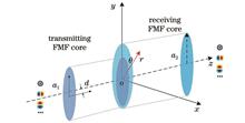
ObjectiveAt present, few-mode fiber (FMF) communication technology, which is popular, is based on mode division multiplexing (MDM). The technology uses the new freedom of mode as an independent channel for information transmission. It can break through the capacity limit of traditional single-mode optical fiber communication and become the key to Tbit/s or even Pbit/s optical fiber communication. FMF fusion splicing is inevitable in the MDM system based on FMF. Therefore, the accurate analysis of the misalignment tolerance of FMF fusion splicing is of great significance for evaluating the fusion-splicing quality and optimizing the matching parameters of FMF, as well as ensuring the reliable and efficient operation of long-distance and large-capacity FMF links. At present, the tolerance of the coupling loss of the fundamental mode LP01 to the transverse offset, rotation angle, and fiber parameter misalignment are the main focus of a priori research. For the FMF that supports multiple spatial modes with coupling between spatial modes, the traditional single-mode fiber LP01 coupling loss theoretical is no longer suitable for analyzing coupling characteristics and misalignment tolerance of FMF fusion splicing. Given the current situation, it is of significance to study the tolerance characteristics of the high-order spatial mode coupling efficiency on the fusion splicing parameters of different transverse offsets and rotation angles under different parameters of FMF.MethodsWe propose a theoretical model based on the Laguerre-Gaussian mode to analyze the misalignment tolerance of FMF fusion splicing. Laguerre-Gaussian mode is utilized to approximate the LPmn mode field distribution of each spatial mode. The coupling efficiency model between LPi mode (transmitting FMF) and LPj mode (receiving FMF) at the FMF fusion splicing is calculated by using the power transmission coefficient. The mathematical model can be estimated as a function of Gaussian waist radius ω, transverse migration d, and angle misalignment θ of the transmitting and receiving FMF. Based on the coupling efficiency model, the tolerance of the spatial mode coupling efficiency at the fusion point to different transverse migrations, rotation angles, and other fusion splicing parameters is analyzed under the welding conditions of different normalized cutoff frequencies and core radius parameters of FMF.Results and DiscussionsThe fusion splicing of six-mode fiber (LP01, LP11a, LP11b, LP21a, LP21b, and LP02 modes) is taken as an example. The numerical analysis results show that under the fusion splicing conditions of different fiber parameters V and a, the coupling efficiency between different spatial modes presents different distribution rules for the tolerance of parameters d and θ. Figures 3 and 4 show the variation curves of the self-coupling efficiency of LP01 mode and the mutual coupling efficiency between LP01 mode and high-order mode with V (normalized cutoff frequency) and a (the core radius of the optical fiber) of FMF parameters under different fusion splicing transverse offsets (0-2 μm), respectively. The analysis shows that the self-coupling efficiency of LP01 increases and then decreases with the increase of V and a. The greater the difference of V and a between transmitting and receiving FMF, the lower the tolerance of LP01 self-coupling efficiency to the transverse offset. Meanwhile, the influence of a on the coupling efficiency tolerance to the transverse offset is greater than that of fiber V. The coupling efficiency between LP01 and the high-order mode also has a similar variation rule. Figures 5 and 6 present the analysis results of the tolerance of spatial mode coupling efficiency to fusion-splicing angle misalignment. Since the field distribution of fundamental mode LP01 is axisymmetric, the self-coupling efficiency of LP01 presents consistent distribution characteristics under different angle misalignments. Similarly, due to the axisymmetric distribution of the LP02 field, the η16 is not affected by the angle misalignment. As V2 increases, the value decreases and then increases. The coupling efficiency between LP01 and degenerate modes LP11a, LP11b, LP21a, and LP21b is affected by sin θ and cos θ factors, and the coupling efficiency is symmetrically distributed relative to the welding angle misalignment. Similarly, the variation trend of coupling efficiency under the condition of a is greater than that of V. Figure 7 shows the efficiency distribution of the self-coupling of LP21a modes and the efficiency distribution of the mutual coupling between LP21a and LP02 mode under different FMF parameters and fusion splicing parameters. Similarly, the coupling efficiency between high-order modes shows regular changes under different angle misalignments and transverse offset fusion. Therefore, it is necessary to strictly control the transverse offset and angle misalignment according to different parameters of FMF fusion splicing to achieve the ideal coupling efficiency.ConclusionsIn this study, a general theoretical analysis model of misalignment tolerance for FMF fusion splicing based on Laguerre-Gaussian mode is proposed given that the traditional single-mode fiber LP01 coupling loss theoretical model is no longer suitable for analyzing the coupling characteristics and misalignment tolerance of FMF fusion splicing. Taking six-mode fiber fusion splicing as an example, the tolerance of the mode coupling efficiency to different transverse offsets and rotation angles of the fusion parameters is analyzed under the welding conditions of different normalized cutoff frequencies and core radius of FMF. The numerical results show that the theoretical model can be used to analyze the tolerance of the spatial mode coupling efficiency to different parameters such as transverse offsets and rotation angles. This model provides a theoretical basis for evaluating the welding quality of FMF and the alignment design and optimization of fusion splicing parameters.
Jul. 25, 2024Vol. 44 Issue 14 1406001 (2024)
Yuhao Lin, Haoqi Du, Zhangjun Yu, Jun Yang, Yuncai Wang, and Yuwen Qin
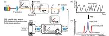
ObjectiveLong-distance polarization-maintaining fiber is mainly used in submarine cables, optical fiber sensor networks, navigation and positioning, geophysical surveys, and other fields. One of the key concerns in the measurement field is the polarization crosstalk of the core component of the optical fiber gyroscope used for navigation and positioning. The optical frequency domain polarimetry (OFDP) is a new polarization measurement method that has advantages such as long measurement distance, high sensitivity, and small measurement times. It can be widely used to accurately characterize polarization-maintaining fibers and their devices. The main performance limitation of OFDP is interference phase error. While some parts of this error, such as the tunable light source’s intrinsic phase noise, sweep frequency nonlinearity, and ambient noise, have been effectively suppressed, residual interference phase noise still exists. This residual noise can degrade the accuracy of polarization crosstalk measurements and is mainly caused by dispersion in the test optical path and birefringent dispersion in the device under test. Existing optical fiber dispersion compensation methods are mostly applied to absolute distance measurements and do not meet the requirements of distributed and transmitted optical polarimeters. We propose an OFDP optical path scheme (SR-OFDP) based on a self-reference interferometer. The accuracy of polarization crosstalk measurement is enhanced through the application of distributed iterative dispersion compensation technology. We hope that the chromatic dispersion verification method and the concept of distributed iterative dispersion compensation proposed in this study will contribute to the advancement of distributed dispersion compensation techniques in the optical frequency domain.MethodsWe first review the basic principles and testing scheme of OFDP. We then theoretically analyze the phase distortion caused by chromatic and birefringent dispersion and discuss the corresponding suppression schemes. Notably, due to the similarity between the phase term introduced by chromatic dispersion and the swept nonlinearity of the light source, it is possible to match the dispersion coefficient by adjusting the length of the delay ring in the interferometer. Then, we employ the SR-OFDP optical path scheme, where phase noise induced by chromatic dispersion in the optical path is eliminated through interpolation resampling. To mitigate the phase error caused by birefringent dispersion in the long-distance polarization-maintaining fiber ring, we propose a distributed iterative dispersion compensation scheme based on optimal criteria. The core idea is to use the criterion function to obtain the total second- and third-order dispersions of the measured fiber, and construct the corresponding dispersion compensation convolution kernel to convolve with the compensated signal, and finally, the phase error of wave number domain is compensated by dispersion in space domain.Results and DiscussionsIn the OFDP accuracy optimization scheme, the experimental design and results for dispersion suppression are shown as follows. Firstly, experiments are designed to identify the source of chromatic dispersion in the optical path. The original single-mode fiber inside the auxiliary interferometer is replaced with a dispersion compensation fiber with a dispersion coefficient of -100 to -200 ps/(nm/km), simulating the case of mismatched dispersion coefficients in the interferometer. When the dispersion coefficients are approximately the same, a 500-meter polarization-maintaining fiber is tested. The amplitude accuracy of the polarization crosstalk peak at the main peak position improves from -25.5 dB to 0 dB, and the spatial resolution increases from 22.41 m to 9.6 cm (Fig. 4), confirming that the dispersion in the measured optical path is caused by differences in the interferometer’s dispersion coefficient. Subsequently, the SR-OFDP optical path scheme is employed to suppress this dispersion (Fig. 5). Based on this optical path, distributed iterative dispersion compensation technique is used to obtain the distributed polarization crosstalk results of a 9.5 km PMF with a sensitivity of -105 dB in 2 s. After dispersion compensation, the amplitude accuracy of the end peak significantly improves by 20 dB (Fig. 6). The forward and backward alignment results of measured fiber dispersion compensation indicate that the dispersion compensation algorithm has good spatial accuracy (Fig. 7). In addition, after dispersion compensation, 10 groups of repeated test results show that the standard deviation of each position along the fiber length is as low as 0.3 dB (Table 1), indicating that the results after the dispersion compensation algorithm exhibit good stability.ConclusionsIn the present study, the dispersion compensation method described is used to improve the accuracy of the polarimeter in the optical frequency domain, filling the gap in fiber dispersion compensation methods for optical frequency domain interferometry. Compared with traditional polarization measurement technologies (such as OCDP), which only satisfy a single index, the SR-OFDP technology with dispersion compensation capability offers distributed measurement, high sensitivity, and long-distance testing. The test speed can reach the order of seconds, and its excellent comprehensive performance is incomparable to other technologies. In the future, OFDP technology will play a key role in the production and fault analysis of high-precision optical fiber gyroscopes, provide more accurate testing means for optical fiber devices, components, and optical paths, and promote the further development of distributed polarization crosstalk testing technology.
Jul. 25, 2024Vol. 44 Issue 14 1406002 (2024)
Bingtao Cai, Limin Xiao, and Xiaobao Chen
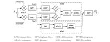
ObjectiveRealizing stable and low-noise phase demodulation is crucial for the highly sensitive detection of weak external signals in interferometric fiber-optic hydrophones. The heterodyne method is one of the most popular phase recovery algorithms due to its ease of hardware implementation and minimal algorithmic complexity. The common heterodyne algorithm involves interfacing acousto-optic modulators (AOMs) of different frequencies in parallel within the two arms of the Mach-Zehnder interferometer (MZI). There are two drawbacks to the aforementioned scheme. The disparate operation of the two independent AOMs introduces additional noise, while the large volume of the AOM-incorporated polarization-preserving optical path hinders effective vibration isolation and renders the system highly susceptible to environmental interference. To address these challenges, we propose the Michelson interferometer (MI) to directly generate front and back dual-pulse light with identical frequency and polarization. Subsequently, the paper utilizes the back-stage AOM serialized on the output optical path to switch the modulation frequency in real time, creating an optical frequency difference between front and rear optical pulses. Unlike conventional schemes, the difference frequency generation optical path has the frequency difference produced by the same AOM without being affected by performance differences in discrete devices. Furthermore, a compact non-bias-preserving MI optical path is devised and assembled to withstand vibrations, enhancing the overall system’s resistance to interference.MethodsFirstly, we provide an overview of the fundamental principles of the heterodyne demodulation algorithm. It is demonstrated through the process of formula derivation that achieving demodulation results with low noise and high stability requires ensuring the algorithm’s high stability in difference frequency and mitigating environmental interference in the optical path. Subsequently, the principle of AOM explains that the primary determinants influencing the difference frequency stability of the algorithm are frequency and amplitude. With the theoretical foundation, the simulation substantiates the influence of difference frequency stability on demodulation noise, as illustrated in Fig. 3. Specifically, frequency and amplitude shifts in the differential frequency lead to a notable degradation of the demodulation noise and subsequent distortion. Analysis of the traditional algorithm’s optical path for difference frequency generation confirms significant inadequacies in both the stability of the difference frequency and its resilience to environmental interference. Therefore, a scheme integrating MI with serial AOMs is proposed, as illustrated in Fig. 5. This enhanced scheme fundamentally addresses the challenges inherent in the traditional scheme. Finally, the experimental optical path before and after the improvement is constructed for a comparison test to validate the theoretical and experimental advantages of the enhanced scheme.Results and DiscussionsBy constructing the actual optical experiment as illustrated in Fig. 7, the results indicate that utilizing the MI with a serial AOM heterodyne scheme yields the demodulated noise power spectral density (PSD) values as low as -90 dB/Hz, -100 dB/Hz, and 104 dB/Hz respectively at the frequency points of 10, 100, and 1000 Hz, as illustrated in Fig. 10. Over 8 hour, the demodulated noise exhibits fluctuations of less than 2 dB at the 10 Hz frequency point, and less than 1 dB at both the 100 Hz and 1000 Hz frequency points, as illustrated in Fig. 11. For the conventional algorithm relying on MZI with parallel AOM, there are distinct high frequency oscillations present in the time-domain signals and multiple spectral lines of various sizes in the frequency domain spectrum, with the overall noise floor being elevated by nearly 10 dB.ConclusionsThe MI-based optical path can effectively avoid the incorporation of a large number of polarization-preserving devices in the difference frequency generation optical path. This scheme greatly reduces the package volume of the optical path structure, simplifies the package scheme, and enhances vibration resistance. Furthermore, the serial use of the AOM ensures that the modulation carriers of the front and back pulse light involved in the interference originate from a singular AOM, significantly reducing additional noise from frequency stability differences between parallel AOMs. The experimental data shows that the proposed difference frequency improved optical path scheme exhibits characteristics such as low noise, absence of conspicuous spurious spectral lines within the bandwidth, and heightened long-term stability in the demodulation of fiber-optic hydrophone signals via the heterodyne algorithm and has substantial engineering applicability.
Jul. 25, 2024Vol. 44 Issue 14 1406003 (2024)
Ying Liu, Mingyang Chen, and Bing Sun
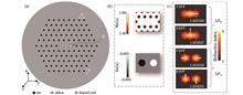
ObjectiveThis study aims to explore the utilization of optical exceptional points (EPs) in non-Hermitian systems, particularly in the context of photonic crystal fibers (PCFs). EPs induce fascinating physical phenomena and applications, such as unidirectional zero-reflection light transmission and phase transitions in metamaterials. Here, we aim to investigate the implementation of EPs in PCFs to achieve mode conversion and modulate optical interactions between different modes.MethodsTo achieve this objective, we introduce a symmetric gain-loss refractive index distribution into the core of PCFs, creating a parity-time (PT) symmetric non-Hermitian system. This approach involves carefully designing and fabricating the PCF structure to ensure the desired refractive index profile. We then analyze the optical properties of the system, including the formation of EPs and their effects on mode coupling and conversion using a beam propagation method.Results and DiscussionsOur investigation effectively showcases the achievement of optical EPs within the tailored PCF architecture, facilitating the proficient manipulation of mode interactions. Specifically, we successfully realize asymmetric mode conversion between LP01 and LP11 modes spanning a wavelength range of 1.3 to 2.0 μm, boasting an efficiency rate of up to 99%. Furthermore, this structure facilitates the simultaneous conversion from the LP11 mode to the LP01 mode (Fig. 5). Leveraging counterclockwise transmission is instrumental in mitigating mode purity issues stemming from device reflections. Crucially, our proposed scheme demonstrates resilient performance across diverse structural parameters, underscoring its promise for practical applications.The observed mode conversion and modulation of optical interactions highlight the significance of EPs in non-Hermitian systems, particularly in the context of PCFs. The symmetric gain-loss refractive index distribution plays a crucial role in creating the PT-symmetric system, forming EPs, and enabling effective control over mode coupling. The high efficiency and tolerance to structural variations further enhance the applicability of the proposed scheme in real-world scenarios.ConclusionsIn conclusion, our study presents an innovative approach for mode manipulation in PCFs based on optical exceptional points. By leveraging the unique properties of EPs in non-Hermitian systems, we demonstrate efficient and flexible mode conversion within a wide wavelength range. This research expands the application scope of EPs in photonics. It provides a promising solution for enhancing the functionality of photonic crystal fibers in various optical systems and devices.
Jul. 25, 2024Vol. 44 Issue 14 1406004 (2024)
Changmiao Wang, Hui Li, Shuiping Zhang, and Yuntao Wu
ObjectiveLight field microscopy (LFM) is widely employed in real-time cellular activity observation, three-dimensional tissue structure imaging, and organ pathological diagnosis. However, the quality of light field microscopic images is often compromised by inherent lens defects and sample-induced optical aberrations due to variable refractive index distributions. Current aberration correction methods primarily exploit the intensity information of the object, ignoring latent sample phase image data such as thickness variations and 3D morphology. Thus, we introduce a phase-intensity dual-path network (PCANet) designed for high-resolution reconstruction in light field microscopic aberration correction and adopt deep learning to decouple two-dimensional light field microscopic intensity and phase information for enhanced resolution. Experimental results indicate that this deep learning approach effectively replaces light field digital adaptive optics, and achieves aberration correction, high-resolution image reconstruction, and restoration of sample detail edges, thereby recovering the resolution and signal-to-noise ratio of light field microscopic imaging.MethodsWe propose a PCANet that combines multi-dimensional light field data with a deep learning model to correct imaging aberrations and perform high-resolution reconstruction. The model consists of two serially processed network segments that handle original low-resolution aberrated light field data, ultimately outputting high-resolution reconstruction via light field microscopic decoupling and PCANet modules. This reduces reliance on complex aberration compensation devices, enabling cost-effective and high-resolution light field microscopic reconstruction. The light field microscopic imaging system captures the original low-resolution aberrated data, which is then decoupled by the light field decoupling module into intensity and phase information. The PCANet extracts features from these dimensions, fusing and mining the two-dimensional sample information to enhance aberration correction and achieve high-resolution reconstruction without hardware compensation. Thus, our deep learning model which requires only low-resolution aberrated light field data as input and outputs high-resolution aberration-corrected images significantly simplifies computation and exhibits superior reconstruction quality in experimental results.Results and DiscussionsThe US Air Force standard USAF is adopted to verify the aberration correction capabilities of PCANet. Reconstruction results show that while the original light field aberration image barely resolves the fifth group of element 2 (line width is 13.92 μm) at the edge, the digital adaptive optics (DAO) method aberration correction reaches the sixth group of element 6 (line width is 4.38 μm). Our process restores the seventh group of element 5 (line width is 2.46 μm), indicating effective aberration correction and high-resolution reconstruction, and near-accurate levels regardless of significant distortion in light field microscopic edges or lesser aberration influences in central areas. Introducing phase information enhances network aberration correction, which outperforms image super-resolution network (VDSR) and Richardson-Lucy deconvolution algorithm (R-Lucy) in horizontal comparisons. Meanwhile, higher peak signal-to-noise ratio (PSNR) and structural similarity (SSIM) performance metrics corroborate the efficacy of our proposed network.ConclusionsWe present an innovative application of deep learning technology to light field microscopic aberration correction, with microscopic samples’ intensity and phase information employed. By conducting resolution plate experiments and tests on egg embryo slices and onion epidermal layers, we demonstrate that the original light field aberration data can be effectively corrected via network recovery to surpass DAO aberration correction methods and R-Lucy deconvolution in terms of reconstructed image resolution and clarity. By decoupling and integrating phase and intensity feature information, our approach avoids complex iterative calculations and additional physical devices, simplifies operations, and reduces system complexity and cost, with potential for practical application advancement.
Jul. 25, 2024Vol. 44 Issue 14 1408001 (2024)
Si Chen, Hui Li, Tian Li, Chenbo Su, and Yuntao Wu
ObjectiveWith rapid development, mixed-reality display systems are increasingly utilized in various fields, such as entertainment, education, and simulation training. However, prolonged use of these systems often leads to visual discomfort for users, posing a significant challenge in this area. The primary cause of user discomfort is the visual accommodation-convergence conflict (VAC), where current mixed-reality display systems often fail to provide the correct focal point. This failure can cause a conflict between the eye’s accommodation and convergence mechanisms, leading to visual strain and discomfort. Utilizing liquid crystal elements in see-through, mixed-reality display systems can resolve the VAC problem. However, the fabrication of liquid crystal devices in these methods is complex, and maintaining high precision in manual production processing is also challenging, potentially affecting the quality of the virtual reality. Hence, there is a pressing need for a simple method in enhanced display systems. We propose a novel approach to achieve see-through light field mixed-reality using polymer dispersed liquid crystal (PDLC), specifically designed to address the visual VAC. The proposed system leverages the electrically adjustable transmittance property of PDLC to seamlessly combine the light field data of the projected target in the real world. A light field rendering algorithm is introduced based on convex optimization theory, which effectively fuses the light field redundancy across different PDLC voltages and the color brightness disparities between the actual scene and the target. This integration generates a visually harmonious image containing the virtual and real fused scenes at varying focal depths. Experiments demonstrate that the proposed system achieves superior quality at a continuous focal depth. The proposed system offers several advantages, including reduced computational demands and affordable hardware expenses.MethodsThe system utilizes PDLC as the core optical element, enabling the combination of light field data from virtual target objects and real scenes. By leveraging the electrically adjustable characteristics of PDLC, the system obtains virtual and real fused light field data at multiple voltages. It implements an adaptive light field rendering algorithm based on convex optimization theory. Two regularization terms are incorporated in the objective function, concerning the device and light field characteristics: A spatiotemporal regularization term considers the redundancy of the captured light field at multiple voltages and uses the redundant information captured at different voltages to refine the details. A harmonized regularization term combines the virtual and real fused light field data captured by PDLC at multiple voltages. It calculates the color brightness difference between the real scene and the virtual object across different color channels, effectively correcting the color of the target virtual object and facilitating seamless fusing with the real scene. The algorithm jointly and optimally reconstructs the multi-voltage virtual and real fused light field data. The data is then decoupled to obtain high-quality two-dimensional images that fuse virtual and real scenes at different depths.Results and DiscussionsThis system investigates the influence of light combiners on see-through mixed-reality display systems, revealing that utilizing PDLC as a light combiner enhances the fusion of reality and virtual elements. This enhancement is attributed to PDLC’s compatibility with the proposed light field rendering algorithm (Fig. 8). Furthermore, we examine the regularization terms of the light field rendering algorithm, affirming that each term positively influences the outcomes. These terms improve color coordination between the virtual and surrounding real environments, consequently enhancing the overall quality of both virtual and real scene images (Fig. 9). To further validate the seamless fusion of real and virtual scenes, we generate coordinated two-dimensional images of real and virtual scenes at various depths of focus (Fig. 10). The results of multiple depths of virtual scene fusion, facilitated by reconstruction based on the light field rendering algorithm, show progressive focus on the virtual letters “A”, “B”, and “C” with changes in depth, maintaining consistent quality with the final real scene. Additionally, the proposed system facilitates relatively smooth zoom effects within the real scene. Compared to conventional mixed-reality systems, the proposed system demonstrates significantly superior virtual reality fusion results (Fig. 11 and Table 1).ConclusionsWe introduce a see-through light field mixed-reality system that leverages PDLC to effectively address the VAC issue. Our method utilizes the electrically adjustable properties of PDLC to seamlessly integrate virtual light field information with real scene light field information. Subsequently, a light field rendering algorithm processes multiple sets of fused virtual and real light field data. Using the redundant information at different voltages of the PDLC and the differences between the real and virtual scenes as constraints, the system generates high-resolution, arbitrary focal depth two-dimensional images that blend virtual and real scenes. Extensive experimental validation demonstrates that the proposed system excels in reconstructing the quality of fused virtual and real scene images. It significantly reduces the visual dissonance of virtual images and supports continuous zoom capabilities. This innovative approach offers an enhanced solution to the VAC problem in existing see-through mixed-reality displays.
Jul. 25, 2024Vol. 44 Issue 14 1411001 (2024)
Yuchang Yan, Linyang Xue, Xiaosa Chen, Guilin Chen, and Changpei Han
ObjectiveIn the Fengyun-4 microwave detection satellite mission, a frequency scanning interferometry (FSI) LiDAR was used to conduct real-time, high-precision measurements of the satellite’s microwave antenna surface profile. This enabled on-orbit adaptive antenna adjustment, ensuring normal operation of the satellite’s payloads. The LiDAR system includes an FSI laser ranging component and a two-dimensional scanning mirror. The precision of the laser ranging system is crucial as it directly influences the accuracy of the antenna surface profile measurements, which in turn impacts the satellite’s overall performance.The laser ranging system uses a distributed feedback (DFB) laser, which modulates the drive current to produce a laser frequency scanning output. However, the output characteristics of DFB lasers tend to degrade with increasing operational duration, particularly under the harsh conditions of geostationary orbit. This degradation can cause a drift in the laser’s frequency scanning characteristics curve, leading to anomalies in the FSI laser ranging system. Consequently, the nonlinearity of the laser frequency scanning should be periodically calibrated and corrected to ensure optimal function of the FSI laser ranging system. Currently, these nonlinearity issues are addressed by iteratively changing the current and using optoelectronic phase-locked loops for active correction. Given the constraints imposed by the harsh space environment, which limits the use of high-performance processors and complex circuits, there is a pressing need for a calibration and correction method that consumes minimal computational resources.Optical fibers, which are primarily used in the FSI laser ranging system to construct internal optical paths, introduce length errors during the fabrication process. Additionally, factors such as temperature changes and laser frequency variations can alter the equivalent optical path length of the fibers, introducing measurement errors. Therefore, periodic calibration of the fiber length or system parameters is necessary. In ground-based conditions, methods such as optical cavities or gas absorption cells are used for fiber length calibration, and precision ranging instruments for auxiliary calibration of the system parameters. However, when deployed as satellite payloads, the use of these optical devices or precision instruments becomes impractical, limiting the applicability of these calibration methods. Thus, there is a need for a calibration process that does not require additional devices or instruments and can rapidly calibrate and correct the parameters of the FSI laser ranging system.MethodsThis study first establishes a mathematical and physical model for the FSI laser ranging system, based on the principles of light interference. It explores the use of an equidistant optical frequency sampling method to derive the fundamentals of an FSI laser ranging system, and investigates the relationship between the measured distance and peak frequency of the beat frequency signal spectrum, standardizing and simplifying the parameter description method. Subsequently, the analysis addresses system errors induced by laser output frequency drift and changes in fiber length. A method is proposed to measure the system’s zero-point by altering the scanning mirror’s pointing angle [Fig. 2(a)], measuring the distance and angle at the targets at both ends of the baseline ruler [Fig. 2(b)], and rapidly calibrating system parameters based on spatial geometric relationships (Eq. 16). Following this, the study delves into the nonlinear error in laser frequency scanning, suggesting a method for calibrating the laser scanning nonlinearity characteristics by linearly modulating the drive current, performing time-frequency analysis on the interferometric beat frequency signals generated by the internal optical path, and constructing a modulation current function to correct for frequency scanning nonlinearity (Eq. 29), accompanied by simulation analysis (Figs. 3 and 4). An experimental setup is then constructed (Fig. 5) using the proposed methods to calibrate the system parameters and correct the laser frequency scanning nonlinearity, with subsequent analysis and discussion of the experimental results.Results and DiscussionsAn experimental setup was constructed to verify the calibration method for the FSI laser ranging system as outlined in this study. The FSI laser ranging system and a baseline ruler were positioned on a large optical platform (Figs. 5 and 6). Following the procedures described in Section 2.3, the scanning mirror was initially controlled to rotate to a position perpendicular to the ranging laser to measure and record the peak position in the spectrum, establishing the system zero-point relationship. Subsequently, the scanning mirror was manipulated to take measurements of the targets at both ends of the baseline ruler, also recording the scanning mirror’s pointing angle and the spectrum peak positions to establish the system linearity (Fig. 7). Experimental data were categorized into four sets, corresponding to different angles of the measuring optical path, distances between the reference scale targets, and center positions of the spectrum peaks. System parameters were calculated using Eq. (16) (Table 1), and an average of the parameters estimated from the four sets was computed to obtain relatively accurate calibration results. Following the protocol in Section 2.4, first, a linear current function was used to modulate the laser, sample the reference beat frequency signal, and conduct time-frequency analyses. Then, a polynomial fitting method was employed to determine the laser frequency scanning nonlinearity function relationship. Finally, a correction current function was formulated using Eq. (29), effectively correcting the laser frequency scanning nonlinearity (Fig. 8).ConclusionsIn response to the measurement errors induced by laser frequency drift in FSI laser ranging systems, this study establishes mathematical and physical models, and conducts formula derivations to determine the expressions for system parameters influenced by the characteristics of lasers and optical fibers. The issue is thus reframed as a calibration problem for the coefficients of linear relationships. The proposed method, which involves altering the scanning mirror angle in conjunction with using a reference scale, measures the system’s zero-point and linear relationships. Subsequently, system parameters are calibrated through geometric relationships. Experiments conducted within a constructed experimental environment validate the accuracy of this method.Addressing the issue of frequency scanning nonlinearity caused by changes in DFB laser characteristics, this paper develops a mathematical and physical model of laser frequency scanning and conducts formula derivations to explore the principles of correcting frequency scanning nonlinearity. A method is proposed for calibrating the laser frequency scanning characteristics by driving the laser with a linear current function, and another method has been proposed for correcting laser frequency scanning nonlinearity by constructing a current function. The validity of these methods is confirmed through simulation analysis and experimental verification.The calibration method for the FSI laser ranging system introduced in this article facilitates automated calibration without the need for manual intervention. This method eliminates the need to augment the existing system with additional optical components such as optical cavities or gas absorption cells. Furthermore, precision instruments, such as high-accuracy displacement stages, laser interferometers, or wavelength meters, are not required for calibration purposes. It is suitable for application in on-orbit deployment and ground testing of the system, demonstrating considerable value for engineering applications.
Jul. 25, 2024Vol. 44 Issue 14 1412001 (2024)
Jinhua Li, Zhaolou Cao, and Gaige Zheng
ObjectiveLayered thin film characterization is significant for the fabrication of micro/nano structures. It is necessary to accurately measure refractive indices and thicknesses of films for ensuring the performance of micro/nano structures. As ellipsometry has high efficiency without intrusion, it nowadays serves as a metrology workhorse for critical dimension determination of nanostructures by comparing measured phase retardation and intensity variation between s/p-polarized reflected beams with theoretical prediction. However, traditional ellipsometry employs a quasi-plane wave to illuminate the sample, resulting in low spatial resolution and potential interference of the reflected light at the other surface for transparent substrates. Additionally, the illumination and detecting arms should be mechanically rotated to adjust the illumination angle for angle-resolved measurements, which requires high stability and reliability. Thus, it is desirable to develop a metrology system capable of measuring without mechanical movements. To this end, we propose a polarization imaging system with a tightly focused vector beam as the light source. As rays from different positions of the aperture provide angle-resolved illumination, the reflected spot images contain information on multi-angle s/p-polarized reflection coefficients, which can be further employed to retrieve film parameters. Compared with ellipsometry, the spot size is close to the diffraction limit in the proposed method, which significantly improves the spatial resolution, reduces the focal depth, and helps avoid mechanical rotation.MethodsA numerical procedure is developed to simulate the reflection of a vector beam on layered films. The amplitude of rays from different positions of the pupil is traced during the reflection based on coordinate system transformation. The angular spectrum theory is adopted to calculate the propagation of focused beams in the free space. By utilizing the proposed numerical method, datasets relating x/y-polarized reflected spot images with different film parameters are created, and a parametric study is performed to examine the sensitivity of reflected spot images to film parameter variation. Meanwhile, we investigate the potential influences of noise on the parameter retrieval accuracy and build an experimental setup to perform the measurement. A linearly polarized plane wave is focused by an objective with a high numerical aperture to generate a tightly focused beam for illumination. The reflected beam is collected by the objective and captured by a camera after being filtered by an analyzer. Film parameters are determined by searching the dataset for spot images that mostly agree with the measured one.Results and DiscussionsNumerical simulation is first performed to deepen the understanding of the dependence of reflected spot images on film parameters. It is shown that a slight variation in film parameters leads to observable changes in x/y-polarized spot images, which demonstrates the high sensitivity of the method. Independent multiplicative noises are deliberately introduced to examine the system robustness. The errors are respectively less than 0.005 and 1.5 nm for the refractive index and thickness while the noise level is 3%. It indicates that due to the information on multi-angle reflection coefficients included in spot images, the system is highly robust against noise influences, which helps lower the requirement for the detection environment. A bare silicon wafer is employed to calibrate the transmission coefficients of the beam splitter for s/p-polarized beams by comparing experimental measurements and theoretically predicted intensity. Commercial single-layer SiO2 films with thicknesses of 100 nm, 200 nm, and 300 nm on silicon substrates are finally measured to validate the system. The discrepancy in thickness measurement between the proposed polarization imaging system and commercial spectroscopic ellipsometry is less than 2 nm. Additionally, variations of thickness and refractive index are less than 0.2 nm and 0.003 in consecutive seven measurements, demonstrating the high stability of the polarization imaging system.ConclusionsIn response to the demand for ellipsometry with a high spatial resolution, we report a polarization imaging metrology system with a tightly focused vector beam for illumination. An experimental setup capable of measuring the reflected light field distribution in different polarization directions is built. Numerical simulation of the reflected light field is conducted and a dataset of the relationship between film parameters and reflected light field is established to retrieve the film parameters. Simulation results show that the reflected light field is highly sensitive to film parameters, which reveals the information of film parameters. Since it contains information on reflection coefficients of multi-angle rays, the system has high robustness against noise and can be adopted to characterize thin films. The experiment on a commercial single-layer SiO2 film on a silicon substrate is performed. The deviation of film thickness is less than 2 nm, and the measurement uncertainty is less than 0.2 nm. Compared with traditional ellipsometers, our polarization imaging system has higher spatial resolution and smaller focal depth. We believe it can find a broad range of applications in nanostructure characterization.
Jul. 25, 2024Vol. 44 Issue 14 1412002 (2024)
Haitao Zhang, and Changqing Xie
ObjectiveAspherical surface testing plays an important role in projection optics for extreme ultraviolet lithography (EUVL) systems and determines the resolution and overlay accuracy of the lithography system. The substrate transmission wavefront error and the pattern placement error are the main factors influencing the accuracy in the metrology of aspherical surface based on computer-generated hologram (CGH), which remains a great challenge to the traditional calibration methods. To this end, a new method for calibrating the wavefront error introduced by pattern placement error based on a triple complex phase is proposed and experimentally studied.MethodsWe propose a triple complex CGH that simultaneously emits three wavefronts for aspheric surface testing, and apply it to wavefront error calibration. By conducting six combined measurements, the manufacturing error and graphic position error of the CGH substrate can be calibrated, and they can also be eliminated in the measurement results. The first measurement is for interferometer TF and RF verification, and with the calibrating method, the surface form of TF and RF can be known. The second measurement is adopted for calibrating the first-order diffraction wavefront of CGH in the +X direction. The third measurement is employed for calibrating the first-order diffraction wavefront of CGH in the -X direction. The fourth measurement is for calibrating the first-order diffraction wavefront of CGH in the +Y direction. The fifth measurement is for calibrating the first-order diffraction wavefront of CGH in the -Y direction and the sixth measurement is to utilize TF and CGH for testing the aspheric surface.Results and DiscussionsBased on the measurement results of test 1-6, TF and RF surface form and tested aspheric surface form can be calculated. The peak-to-valley (PV) value of TF surface form is 74.2 nm and root mean square (RMS) error is 13.9 nm. The PV value of RF surface formform is 53.3 nm and RMS error is 6.6 nm. The PV value of surface form of the tested aspheric surface is 31.6 nm and RMS error is 4.88 nm. The same tested aspheric surface is also measured by refraction null compensation test, and the tested PV value is 38.6 nm and RMS error is 5.14 nm. The comparison between the two results indicates that the proposed method has subnanometer RMS accuracy.ConclusionsAspherical surface testing plays a vital role in projection optics for EUVL systems, and determines the resolution and overlay accuracy of the lithography system. The substrate transmission wavefront error and the pattern placement error are the main factors that influence the accuracy in the metrology of aspherical surface based on CGH, which remains a great challenge to traditional calibration methods. Therefore, we propose a triple complex CGH that simultaneously emits three wavefronts for aspheric surface testing and apply it to wavefront error calibration. By carrying out six combined measurements, the manufacturing error and graphic position error of the CGH substrate can be calibrated, and they can be eliminated in the measurement results. The PV value and RMS error are 31.6 nm and 4.88 nm for a tested aspheric surface respectively. Furthermore, the same aspheric surface is also measured by a refractive aspherical null testing system, with the corresponding PV value and RMS error being 38.6 nm and 5.1 nm respectively. This method intrinsically has the subnanometer accuracy necessary for EUVL aspherical optical components.
Jul. 25, 2024Vol. 44 Issue 14 1412003 (2024)
Zhiming Luo, Yifei Zhou, Rui Li, and Zhenyu Jiang
ObjectiveThe temporal phase shifting method is a widely used non-contact optical measurement method, with the advantages of full-field measurement, high speed, and high precision. Although the idea of phase unwrapping itself is simple, the irregular phase truncation contour caused by complex topography and various noises in the phase principal value image often inhibits the effect of the direct phase unwrapping method. In order to improve the measurement ability of complex topography and reduce the interference of noise, we propose a simple and effective phase unwrapping method for temporary phase shifting fringe projection profilometry by introducing the stereo digital image correlation (DIC) method.MethodsFirst, four-step phase shifting fringe patterns are projected and collected, and an additional speckle pattern is projected onto the surface of the object to be measured, then the wrapped phase is calculated. Second, the Canny edge detection method is used to determine the position of the grayscale-jump contour line in the phase principal value image. Third, the depth of the pixels on contour line is calculated by DIC method. Fourth, the phase of the pixels on the contour line is estimated via the stereo DIC method. Fifth, the fringe order of the contour line is calculated based on the estimated phase. Sixth, the fringe order of the phase continuous region between the contour lines is calculated according to the fringe order on the contour lines. Lastly, the fringe order of the phase continuous region between the contour lines is combined with the fringe order on the contour lines to complete phase unwrapping.Results and DiscussionsThe experiment shows that this method can achieve the measurement accuracy of the conventional multi-frequency heterodyne method, and it shows good adaptability to complex surface morphology and discontinuous phase distribution. It can automatically complete accurate phase unwrapping without human intervention.ConclusionsThe proposed method requires measuring only a small number of pixels using stereo DIC method. These pixels account for less than 10% of the total number of effective pixels. After the phase information of these pixels is obtained, a relatively simple and direct algorithm can be used to process pixels in other areas. Our method provides an effective means to handle complex surface phase measurement and offers a new idea for the situation requiring high measurement speed.
Jul. 25, 2024Vol. 44 Issue 14 1412004 (2024)
Differential Motion Grating Displacement Measurement System Based on Moiré Fringe Projection Imaging
YaoYunfei, and Xu Gao
ObjectiveWith the continuous progress in semiconductor chip manufacturing processes, nanoscale-precision measurement technology has become an urgent scientific research problem to be solved. Grating displacement measurement technology has attracted the attention of domestic and foreign researchers owing to its high accuracy, robustness, and other advantages. In recent years, research on grating displacement measurement systems has continued, but some problems remain. Most systems use four split-phase sine-wave photoelectric signals for displacement measurement, which requires the introduction of a large number of optical components in the optical path, making it difficult to miniaturize the system. With this method, it is difficult to break the limitations of the grating processing level, and the demodulation error of phase edge information is also relatively large. In addition, the matching high frequency subdivision technology and subdivision error correction technology are relatively mature, making it difficult to continue improving the system resolution and accuracy. To further improve the resolution and accuracy of the grating displacement measurement system and achieve miniaturization of the system, this paper proposes a differential grating displacement measurement system based on Moiré fringe projection imaging.MethodsImage-based measurement systems based on the principle of grating polarized light interference have various advantages, and the traditional photoelectric conversion systems can be transformed into digital image processing systems. The use of image processing methods with the displacement amplification characteristics of Moiré fringes avoids the limitations of current grating processing systems for high-precision and high-resolution displacement measurements. Improving system measurement accuracy and resolution while reducing the use of multiple spectroscopic prisms makes miniaturization easier.Results and DiscussionsA high-resolution single-grating displacement optical sensing system was designed for the projection imaging of Moiré fringes (Fig. 1). Compared with traditional systems, the special design of the reading head enables the system to achieve four optical subdivisions of the measured grating period with only one diffraction. The design improves the basic resolution of the system and replaces the traditional photoelectric conversion system with a digital image processing system. It avoids the problem of adding multiple light-splitting prisms and optical mirror groups in the optical path owing to the phase-shift measurement requirements of traditional photoelectric conversion systems, making it easier to achieve miniaturization. A mathematical model of the image-based displacement sensing signal was derived. Based on the optical mechanism of Moiré fringe imaging, specific calculations were carried out on the scribing, flatness, installation, and adjustment errors of the grating (Fig. 4), which is the core component of the system. This further explained the relationship between the maximum allowable speed of the dynamic operation of the system and frame rate(Fig. 5). Simulations and design performance analyses were conducted for the system (Figs. 6-8). As shown in Fig. 6, the spot energy generated by the system is concentrated at the center of the detector and has a good degree of overlap, providing high-quality image signals for the subsequent demodulation. As can be observed in Fig. 7, the system ultimately presents a clear Moiré fringe pattern on the detector image plane. By using image processing methods to count and subdivide the stacked grating patterns, the displacement of the grating can be measured. As depicted in Fig. 8, the distribution of the grayscale extreme value curve after interpolation and subdivision is consistent with that of the original image, and the stripe centerline is located at the brightest point of the stripe center. It can be observed from the demodulation results that when using a diffraction grating with a measurement grating of 1200 line/mm, the system has a resolution of 2.075 μm before subdivision. After subdivision, the resolution reaches the nanometer/sub-nanometer level.ConclusionsA differential grating displacement measurement method based on Moiré fringe projection imaging is proposed to overcome the limitations of traditional grating displacement measurement systems that rely on four split-phase sine-wave photoelectric signal measurements. Based on the principle of grating polarized light interference, image processing methods, and displacement amplification characteristics of Moiré fringes, the limitation of the current grating processing level in high-precision displacement measurements is avoided. A high-resolution single-grating displacement optical sensing system for projection imaging of Moiré fringes is designed, which realizes the acquisition of four-fold optical subdivision displacement signals and completes the image conversion of displacement signals using a CMOS image detector. A mathematical model of the image-based displacement sensing signal is derived. Based on the optical mechanism of Moiré fringe imaging, specific calculations are performed on the scribing error, flatness error, installation, and adjustment error of the grating, which is the core component of the system. Simulation and design performance analyses are conducted on the system, which further explain the relationship between the maximum allowable speed of the dynamic operation of the system and the frame rate. At the maximum allowable speed of 0.048 mm/s, the basic resolution of the system can reach 2.075 μm; after subdivision, the resolution can reach the nanometer/sub nanometer level.
Jul. 25, 2024Vol. 44 Issue 14 1412005 (2024)
Fupei Wu, Junlong Peng, Weilin Ye, Zhidan Zheng, and Shengping Li
ObjectivePrinted circuit board (PCB) is a crucial component of electronic products, and its mounting quality directly affects the stability and reliability of electronic products. Therefore, three-dimensional (3D) reconstruction of PCB is essential for accurately detecting solder joint defects and component mounting positions, etc., which is vital for ensuring PCB mounting quality. At present, the structured light method is widely used in PCB 3D reconstruction due to its simple operation, versatility, and high precision. However, the accuracy of PCB 3D reconstruction is compromised by two main factors. First, the varying reflectivity of the PCB surface can lead to abnormal and missing fringe phase information. Second, calibration errors of the structured light system can further affect accuracy. We propose a PCB 3D reconstruction method based on fringe phase characteristics, which effectively addresses the issue of missing 3D point clouds when measuring high dynamic range surfaces and improves the accuracy of 3D reconstruction.MethodsThe structured light system consists of a structured light generator and a camera. Initially, a multi-exposure image fusion rule based on adaptive weights is established, which calculates the weight map through sample images captured at different exposure time and synthesizes the fringe image sequences. The weight map is determined by two factors: the relationship between each pixel’s intensity value and the overall brightness of the current image, and the variation of the same pixel between neighboring exposure images. Next, the phase value is solved using an asynchronous multi-frequency phase shift method. To improve the calibration accuracy of the structured light system, we build a height reconstruction model based on the perspectives of the camera and the structured light generator. The optimal function is formulated by examining the offset between the measured value and the actual value of the gage blocks. Subsequently, the Levenberg-Marquardt algorithm is used to fit and optimize the 3D reconstruction parameters in the optimization function. Finally, the 3D reconstruction results of the proposed method are verified using selected dark and high reflectivity areas on the PCB surface, and the accuracy is confirmed with a standard ball.Results and DiscussionsOur method can effectively optimize the image intensity of the dark region and saturated region while preserving the structure of the fringe in the synthesized image. This significantly addresses the issue of fringe loss on the surface with complex reflectivity (Fig. 7). In addition, the accuracy and stability of surface phase calculation are enhanced by increasing phase shift steps in the main phase shift fringe sequence, which greatly influences phase unwrapping precision. Consequently, the proposed method can accurately reconstruct the 3D shape of the measured objects (Fig. 8) and the reconstruction rate of the samples is 98.3% (Table 3). The performance of the proposed method is significantly superior to the other three methods. In the precision evaluation experiment, the average diameter error of the standard ball measured by the proposed method is 0.0188 mm and the root mean square error (RMSE) is 0.0441 (Table 4). These results demonstrate that the proposed method can reduce the error in 3D reconstruction parameters using gage blocks to further optimize the parameters of the camera and the structured light generator. When compared to the PCB 3D reconstruction results of the triangular stereo model and phase-height model, the proposed method exhibits better accuracy and stability, leading to improved measured outcomes.ConclusionsTo improve the accuracy and reliability of PCB 3D reconstruction, we propose a method based on fringe phase characteristics. The main conclusions are as follows. Firstly, the multi-exposure image fusion method based on adaptive weights is used to synthesize the coded fringe images, and the phase field is then solved using the asynchronous multi-frequency phase shift method, enhancing the measurement success rate for high dynamic range and complex surface. This approach effectively addresses the issue of missing point clouds on high dynamic range surfaces. Secondly, the system calibration error, caused by camera error transmission and simplification of the structured light generator model, is reduced using gage block constraints to optimize 3D reconstruction parameters. Thirdly, experimental results demonstrate that the proposed method can accurately reconstruct the 3D shape of high dynamic range and complex surface and significantly reduce the problem of point cloud loss. In the precision evaluation experiment, the proposed method measured the average diameter of a standard ball with a diameter of 20.0148 mm, achieving an average diameter error of 0.0188 mm. Compared to the triangular stereo model and the phase-height model, the proposed method offers superior precision and stability in PCB measurement results.
Jul. 25, 2024Vol. 44 Issue 14 1412006 (2024)
Yu Dai, Wenxi Zhang, Xinxin Kong, Sizepeng Zhao, Hao Xu, and Zhetao Deng
ObjectiveOptical fibers have been widely used in various industries, national defense, and information technology due to their flexibility, low transmission loss, small size, and light weight. To avoid phase changes in optical fibers caused by environmental vibrations and temperature drift, a combination of fibers and free space optics is often used to construct a circulator device in typical applications, such as Doppler wind lidar and laser Doppler vibrometer systems. Alignment error is the main source of decreased coupling efficiency between fibers and free space optics. Many theoretical studies have examined the impact of mismatch factors on coupling efficiency, such as tilt and misalignment of fibers on coupling efficiency. However, few methods exist for detecting the relative spatial position information of optical fiber such as tilt and dislocation. Conventional detection methods, including the energy monitoring method and far-field coincidence monitoring method, cannot quantitatively analyze fiber mismatch factors. The coupling efficiency is related to the wavefront correlation coefficient between the two fibers, which is determined by their relative position. Monitoring the correlation between the two fiber wavefronts can guide assembly and quantitatively evaluate the coupling efficiency of this type of circulator. The phase detection technology based on Hertz-level frequency-shifting heterodyne interferometry can theoretically determine the wavefront correlation coefficient of the two fibers, which is related to the PV (Peak to valley) value of the interference wavefront.MethodsBased on the theory of Hertz-level frequency-shifting heterodyne interferometry, the sources affecting the demodulated value of the interferometric phase are analyzed. The acousto-optic modulator (AOM) frequency is further segmented into fixed and random frequency for analysis. The parameters related to the detector including fixed frame frequency deviation and shot noise are analyzed.Results and DiscussionsA linear relationship is found between transverse displacement and PV value, with a slope of 0.139λ μm-1. The change in PV value, δPV<0.002λ, caused by the fixed deviation of AOM frequency, within the range of ±0.2 Hz from the nominal value, is two orders of magnitude smaller than the PV value caused by the relative spatial position of the optical fiber. Similarly, when the fixed deviation of frame rate is within the range of ±1 Hz, the PV change is also two orders of magnitude smaller. The impact of shot noise on PV variation is generally less than 10-3λ, mainly influenced by factors such as the quantum efficiency, pixel size, and bandwidth of the detector. Based on the simulation results, the selection of experimental devices is carried out. Lumentum 1103P He-Ne laser tube is used for the laser. The low-frequency heterodyne drive circuit with a 5 Hz frequency offset is self-developed. The frequency offset measurement data of the drive circuit shows a frequency range of (5±0.1) Hz. The visible camera SUA230 of Hua-Teng Vision is selected for the detector, with an image area size of 7 mm×7 mm and a pixel size of 5.86 μm. The parameter α related to the shot noise is calculated to be 3.3 calculated based on quantum efficiency and other parameters. In an experiment with 50 consecutive measurements, the mean PV value is 0.2167λ with a standard deviation of 0.0059λ.ConclusionsThe influence of frequency deviation of the acousto-optic frequency shifter, the frame frequency deviation of the detector, and shot noise on the measurement accuracy of the heterodyne wavefront detection system are studied, and the influence formula is derived. The effects of the fixed frequency deviation of the acousto-optic frequency shifter, random frequency deviation of the acousto-optic frequency shifter, fixed frame rate deviation of the detector, and detector shot noise on measurement accuracy are simulated and analyzed. When the wavefront PV caused by transverse displacement is within one wavelength, the PV value change due to fixed and random frequency deviations of the acousto-optic frequency shifter is within ±0.2 Hz. When the fixed frame rate deviation of the detector is within the range of ±1 Hz, the PV value change caused by it is also in the order of 10-3λ. The impact of shot noise on the wavefront is mainly related to the working bandwidth, quantum efficiency, and pixel size of the detector, and the PV value change caused by it is generally not more than 10-3λ. According to the analysis results, the heterodyne wavefront detection device is built, and the measurement resolution is better than 0.01λ, which verifies the relevant theory. The detection device can accurately characterize the correlation between the two wavefronts, providing a technical means for the quantitative characterization of this type of circulator, and effectively improve the performance of LIDAR and laser Doppler vibrometers using this type of circulator.
Jul. 25, 2024Vol. 44 Issue 14 1412007 (2024)
Kuan Yan, Cong Zhang, Xubing Chen, Mingchao Li, Jie Fang, and Dong Ye
ObjectiveLaser soft soldering in the field of electronic assembly is a high-precision welding technology mainly used for the welding of small and precision components. The laser soft soldering system uses a semiconductor laser as the heat source to provide a highly concentrated laser energy beam to achieve high-quality welding with fast processing speed, a small heat-affected zone, and high precision. In the machining system, the performance of the semiconductor laser directly affects the welding effect with current and temperature being critical parameters to control. These parameters directly affect the focusing and energy distribution of the laser beam. Semiconductor lasers, also known as laser diodes, are electro-optical conversion devices. During processing, part of the electrical energy is converted into heat, causing the temperature to rise. This rise in temperature decreases the efficiency of the semiconductor material and the laser’s output power. Excessive temperature leads to laser wavelength drift, affecting the interaction between the laser beam and the material. Conversely, too low a temperature can make the laser difficult to start and result in unstable output power. Therefore, to ensure the performance and reliability of semiconductor lasers, it is crucial to develop a temperature control system to maintain temperature stability.MethodsTo address these issues, we propose a temperature control system for semiconductor lasers based on a model predictive controller (MPC). First, a mathematical model is established for the thermoelectric cooler (TEC) and other components of the thermal control apparatus. Subsequently, a predictive control model for the laser’s thermal control system is constructed using this mathematical model and software simulations. Finally, the feasibility of the design is validated through practical experimentation on an experimental platform specifically designed for laser soldering processes. The experimental verification involves actual laser soldering operations, confirming the practicality of the proposed design.Results and DiscussionsTemperature fluctuations in a semiconductor laser can lead to instability in its output power, affecting the quality of the laser and the effectiveness of soldering. An increase in temperature alters the physical properties of semiconductor materials, such as the band structure and carrier concentration, which in turn affect the wavelength and intensity of the laser. To verify the effectiveness of this design in controlling the laser’s temperature under varying input currents, we design an experiment to assess the thermal control capabilities under randomly changing laser input current conditions. Experimental results indicate that under MPC, the laser temperature converges rapidly and remains stable (Fig. 6), with energy consumption being about 42% lower than that under proportional-integral-derivative (PID) control (Table 1). In the laser center wavelength stability experiment, the center wavelength shift measurement experiment of the semiconductor laser is designed to indirectly evaluate the junction temperature control stability of the semiconductor laser under the control of MPC. The drift fluctuation range of the central wavelength of the laser under MPC thermal control system is 0.36 nm within 30 min, which is 52% less than that of PID control (Fig. 7). Experiments on laser soft soldering capabilities show that under MPC control, the laser can efficiently complete soft soldering tasks, achieving reliable and effective solder joints (Fig. 9).ConclusionsTo enhance the control performance of the thermal management system in the semiconductor laser of the laser soft soldering system, we conduct precise mathematical modeling based on thermoelectric cooling devices and non-equilibrium thermodynamics principles. This leads to the design of an MPC for the thermal control system. The effectiveness of the control algorithm and the actual laser soft soldering capabilities are validated through experiments. Under simulated conditions, a comparative study between the traditional PID control algorithm and the MPC control algorithm indicates that under random input current changes within the working current range of the laser, the MPC-based thermal control system offers more stable and rapid temperature control. The temperature overshoot is reduced to 1.12%, significantly shortening the time and range of temperature fluctuations of the semiconductor laser during operation. In addition, the energy consumption of the entire thermal control system is reduced by about 42%. Under real processing parameters and environment, the MPC algorithm-based thermal control system produces a solder joint temperature curve that closely matches the ideal temperature curve compared to the PID control algorithm. The average stabilization time is 42.53 ms, with better robustness and higher reliability and quality of solder joints, meeting the stringent thermal control requirements of the laser soft soldering field.
Jul. 25, 2024Vol. 44 Issue 14 1414001 (2024)
Han Zhou, Xuchu Wang, and Yue Yuan
ObjectiveWe aim to enhance the performance of point cloud registration tasks. In recent years, attention mechanisms have shown great potential in 3D vision tasks such as point cloud registration. Currently, the lack of depth interaction during the feature extraction stage may result in the loss of important latent similar structures, thus degrading the performance under low-overlap scenarios. To this end, we propose a 3D point cloud registration network called DIM-RFNet based on deep interactive multi-scale receptive field features, which combines structural context consistency to identify latent similar structure features for efficient point cloud registration.MethodsThe proposed DIM-RFNet model includes two stages. In the coarse registration stage, the sampled point cloud is input into the neighborhood patch feature extraction module to obtain the neighborhood patches and feature information matrix. Then, the information is fed into the context structure encoder, embedding the neighborhood patches into a high-dimensional space and aggregating different-scale features. These features are further input into a transformer to update the high-dimensional features. The context structure decoder continuously expresses the neighborhood patches and corresponding high-dimensional features using a multi-layer perceptron (MLP), ultimately outputting a set of key points and their dimension-reduced structural features. In the fine registration stage, the key points and features obtained during the coarse registration stage are input into the overlap relation encoder, which employs structural feature cross-attention and self-attention to predict pairs of points with overlapping relations, leading to an overlap relation confidence matrix. The top K pairs with the highest overlap relation confidence are selected and input into the overlap relation decoder, which outputs feature representation, overlap score, and match score.Results and DiscussionsOur method is extensively evaluated on synthetic datasets ModelNet40 and ModelLoNet. The experiments demonstrate that DIM-RFNet outperforms other comparison methods in registration time error (RTE) and correspondence distance (CD) for highly overlapped ModelNet40. Experiments on real indoor scene datasets 3DMatch and 3DLoMatch indicate DIM-RFNet’s ability to reliably predict overlap relations under low-overlap scenarios. Experiments on the real outdoor scene OdometryKITTI dataset reveal that DIM-RFNet’s performance on rotation root mean square error (RRE) and translation root mean square error (RR) is superior to other methods, proving DIM-RFNet’s suitability for large-scale outdoor scenes.ConclusionsWe introduce DIM-RFNet based on deep interactive multi-scale receptive field features. DIM-RFNet adopts a coarse-to-fine registration strategy, leveraging graph structure and edge information from unordered points to obtain neighborhood patches and feature information matrices. Meanwhile, the proposed DIM-RFNet is evaluated on public ModelNet, ModelLoNet, 3DMatch, 3DLoMatch, and OdometryKITTI datasets, and comparative experiments demonstrate that it has yielded competitive improvement under low-overlap scenarios.
Jul. 25, 2024Vol. 44 Issue 14 1415001 (2024)
Nanxi Lin, Xinpan Yang, Chenjun Xu, Huaqin Wu, Hong Zhang, Naifeng Zhuang, and Xiaolin Hu
ObjectiveMagneto-optical crystals are pivotal components that determine the performance of magneto-optical devices. Through the hybridization between the excited Bi3+ 6p orbital and Fe3+ 3d orbital, the modification of superexchange induces a strong mixing between crystal field states of varying energies, greatly enhancing the magneto-optic effect in ferrite. Doping Bi3+ ions emerges as a key approach to enhancing the magneto-optical properties of commercial Y3Fe5O12 (YIG) crystals. However, despite being the only known room temperature single-phase multiferroic material, there is scarce literature reporting on the magneto-optical properties and its applications in magneto-optical devices of the perovskite BiFeO3 with a high concentration of Bi3+. This can be attributed to its unique spiral G-type antiferromagnetic structure, which exhibits weak macroscopic magnetism. Additionally, due to its trigonal crystal system and birefringence effect, BiFeO3 demonstrates a considerably feeble magneto-optical effects. In the present study, stable pure phase cubic BiFeO3 single crystals are grown by doping Sr2+ and Ti4+ ions. This eliminates the birefringence effect of the trigonal BiFeO3 and induces strong magnetic and magneto-optical effects, providing a useful reference for exploring high-quality, large-size new magneto-optical crystals suitable for high-performance magneto-optical devices.MethodsBi2O3 is chosen as the self-flux solvent, and a series of crystals including Bi1-xSrxFeO3 and Bi1-xSrxFe1-xTixO3 (x=0-0.5) are grown by using the molten salt method. The crystal structure and lattice parameters of Sr∶BiFeO3 and Sr/Ti∶BiFeO3 are determined by XRD spectra analysis and Rietveld refinement. The structure and morphology changes of BiFeO3 crystals are observed by scanning electron microscopy (SEM). Elemental valence states in the crystals are analyzed using X-ray photoelectron spectroscopy (XPS), while magnetic properties and magneto-optical performance are characterized by a vibrating sample magnetometer and magneto-circular dichroism spectroscopy respectively.Results and DiscussionsThe Rietveld refinement results show that Bi0.7Sr0.3FeO3 and Bi0.7Sr0.3Fe0.7Ti0.3O3 crystals belong to the Pm3¯m space group of the cubic crystal system. The cell parameters of Bi0.7Sr0.3FeO3 and Bi0.7Sr0.3Fe0.7Ti0.3O3 crystals are 3.9517 Å and 3.9447 Å, respectively. The SEM images also prove that BiFeO3 changes from a triangular columnar crystal to regular cubic crystals. When the cooling rate of crystal growth is controlled within the range of 1-10 ℃/h, the size of cubic crystal grains are 20-50 μm. Sub-millimeter size crystal grains are obtained when the cooling rate of crystal growth is 0.5 ℃/h. However, as the grain size increases, the distance between the stress field of the dislocation packing group and the dislocation source in the crystal also increases, resulting in a stronger stress field and subsequent grain deformation. XPS spectra show that doping of heterovalent elements leads to the production of Fe2+ and high-valence iron. The saturated hysteresis loop and MCD spectra indicate that the magnetic and magneto-optical properties of BiFeO3 crystal can be significantly enhanced by doping of Sr2+ and Ti4+ ions, but the coercivity has not significantly changed. The saturation magnetization of Bi0.7Sr0.3Fe0.7Ti0.3O3 is observed to be 0.31 (A·m2)/kg, which is approximately four times that of BiFeO3, while exhibiting a significant MCD ellipticity value (ψF) of 179 (°)/cm, in contrast to the negligible MCD signal produced by BiFeO3 (Fig. 7 and Fig. 8). This can be attributed to the introduction of Sr2+ and Ti4+ ions, leading to the elimination of the birefringence effect, as well as the suppression of the periodic spiral spin magnetic structure and providing additional electronic transition pathways. Consequently, this enhances both the magnetic and magneto-optical properties of BiFeO3 crystals.ConclusionsA series of non-birefringent cubic Bi1-xSrxFeO3 (x=0.3, 0.4, 0.5) and Bi1-xSrxFe1-xTixO3 (x=0.2, 0.3, 0.4, 0.5) crystals are grown by using the molten salt method. The introduction of Sr2+ and Ti4+ ions causes lattice distortion of BiFeO3 and inhibits its periodic helical spin magnetic structure. Especially, when Ti4+ ions are introduced to replace part of Fe3+, the helical G-type antiferromagnetic structure of BiFeO3 will be broken, thereby releasing part of the spin magnetic moment of Fe ions. This results in the magnetism and magneto-optical effects of Sr∶BiFeO3 and Sr/Ti∶BiFeO3 are significantly stronger than that of BiFeO3. The saturation magnetization of Bi0.7Sr0.3Fe0.7Ti0.3O3 is approximately 4 times that of BiFeO3. Its MCD ψF value is observed to be 179 (°)/cm, which is about 4.5 times that of YIG, a popular commercial magneto-optical material tested under the same conditions. With high saturation magnetization, low coercivity and strong magneto-optical effect, Sr/Ti∶BiFeO3 crystals are expected to be used as core magneto-optical materials in magneto-optical modulation, magneto-optical sensing, magneto-optical imaging and other devices, and are hopefully applied in optical communication, laser display, biomedicine, etc.
Jul. 25, 2024Vol. 44 Issue 14 1416001 (2024)
Manli Tian, and Changxi Xue
ObjectiveAugmented reality head-up display (AR-HUD) systems can project driving information in the form of images or text into a driver’s field of view, providing real-time and intuitive driving information and enhancing driving safety. The focal point of vision changes with vehicle speed according to the characteristics of the human eye. However, traditional AR-HUD systems can only project images at a fixed distance, which not only fails to achieve the ideal AR effect, but also leads to visual fatigue. Existing variable imaging distance AR-HUD systems use off-axis reflection structures to adjust the position of the first mirror or the position and size of the picture generation unit (PGU) to change the projection distance. However, they can not simultaneously satisfy the different imaging distance requirements for basic and interactive information. Therefore, it is necessary to propose a variable imaging distance AR-HUD system that can display basic and interactive information separately.MethodsThe initial structure of an off-axis three-mirror system is generally based on the design of a coaxial three-mirror system, but the final structure usually deviates significantly. This intermediate process also requires considerable time. This study constructed an aberration evaluation function for off-axis reflective systems based on vector aberration theory and used a global optimization algorithm to find the optimal solution for the evaluation function, directly obtaining the initial structure of the off-axis three-mirror system. Two PGUs were used to construct near- and far-field optical paths to design a dual-focal-plane AR-HUD system. Referring to the zoom principle of coaxial systems, to ensure that the positions of the PGUs remain unchanged during changes in the imaging distance, it is necessary to adjust the spacing of the two mirrors. However, in this study, the near- and far-field optical paths shared the same freeform mirror. To ensure that the changes in the imaging distance of the far-field optical path do not affect the near-field optical path, the shared freeform mirror must remain stationary. If an off-axis three-mirror structure is used in the far-field optical path, it is impossible to ensure that the positions of the PGUs remain unchanged without affecting the near-field optical path. Therefore, a flat mirror was added to the far-field optical path, which did not change the position of the freeform mirror. By changing the spacing between the two flat mirrors, a change in the imaging distance was achieved. Using Zemax’s “Macro” to obtain the relevant parameters during the change in imaging distance, curves of the movement distance of the mirrors and change in image size on the PGU during this process were plotted. The image quality was evaluated and a tolerance analysis was conducted.Results and DiscussionsThe imaging quality of the dual-focal-plane AR-HUD system was analyzed at projection distances of 2.5 and 10 m, with a pupil size of 6 mm. At both distances, the size of the spot at the center and worst imaging position at the edge of the RMS radius of the spot diagrams are smaller than those of the Airy spot (Figs. 6 and 9). The MTF at 6 lp/mm is greater than 0.3 at both distances (Figs. 7 and 10), and the grid distortions are all less than 5% (Figs. 8 and 11). By adjusting the projection distance, the variation in the distance between the mirrors during the imaging-distance change process is plotted (Fig. 13), as well as the variation curve of the image size on the PGU (Fig. 15). During the change in imaging distance from 10 to 20 m, the movement distance of the two flat mirrors does not exhibit any abrupt changes and can be continuously adjusted, ensuring that the PGU position remains unchanged. Imaging distances of 15 and 20 m validate the imaging quality during the distance-change process. A field of view box of 120 mm×60 mm is obtained, with field angles of 5°×1° and 10°×5° and virtual image distances of 2.5 and 10-20 m for the dual optical path heads-up display system. The imaging quality meets the design requirements, and the tolerance analysis demonstrates the stability and manufacturability of the system.ConclusionsThe dual-path AR-HUD with variable projection distance not only reduces driver visual fatigue but also meets the different imaging distance requirements for basic and interactive information. Near-field path imaging is located on the hood, 2.5 m from the driver’s eyes, to prevent interference with the vehicle in the front, whereas far-field path imaging is positioned at 10-20 m, enabling better integration with the real scene. To ensure that changes in the far-field path imaging distance do not affect near-field path imaging, and to maintain the PGU position unchanged, an off-axis four-reflective structure is designed for far-field path imaging. This system can achieve multilevel, different-depth information displays according to the actual application, significantly enhancing the driver’s visual experience and information interaction effects.
Jul. 25, 2024Vol. 44 Issue 14 1422001 (2024)
Zhe Wang, Zhong Sheng, Jingzhen Han, Zheng Zhen, Chengran Zhang, Dechao Ma, and Mingxu Piao
ObjectiveTraditional infrared optical systems are typically bulky and comprise numerous lenses. To achieve miniaturization, planar imaging elements with microstructured surfaces are often employed. However, these complex surfaces can pose processing challenges and increase costs. This study introduces a planar diffractive element that integrates Fresnel and diffractive surfaces to address the aforementioned issues. Diffractive optical elements possess unique dispersion and temperature characteristics. By combining a diffractive surface with a Fresnel surface, the optical system’s structure can be simplified, reducing its weight and achieving performance indices that are difficult for traditional systems to match. This approach is characterized by ease of processing and low cost. Increasing the field of view exacerbates off-axis aberrations, leading to diminished image quality. Analysis of these aberrations indicates that coma and field curvature are the primary monochromatic aberrations affecting Fresnel and diffractive surfaces. To address this, we propose a design method incorporating computational imaging to correct off-axis aberrations in planar diffractive elements, even as the field of view expands.MethodsThe formulas for monochromatic aberration in Fresnel and diffractive surfaces have been derived. Coma and field curvature become the primary monochromatic aberrations as the field of view increases. Therefore, correcting off-axis aberrations in optical design focuses on astigmatism, while coma and field curvature are addressed in the computational imaging phase. The imaging process in the optical system is essentially one of image degradation. The final image is obtained by passing a clear image through the optical system, convolving it with the point spread function (PSF), and adding noise. Thus, the PSF can be used as a restoration function to deconvolve the imaged image and obtain a clear image. A wavefront aberration model of the optical system is established using Zernike polynomial fitting. A PSF model is constructed using the Fourier transform. The blurred image is restored using a deconvolution algorithm. Differences in the PSF model at object distances of infinity and 4 m are discussed, and the data sizes of evaluation functions at different object distances are compared. The diffraction efficiency of the planar diffractive element at long-wave infrared wavelengths is calculated, addressing the need to determine its efficiency.Results and DiscussionsA planar computational diffractive optical system with a component thickness of 1 mm is designed to achieve miniaturization (Table 1). A PSF model, constructed using computational imaging methods, is employed for restoring blurred images. The restored image is evaluated based on power signal-to-noise ratio (PSNR) and structural similarity (SSIM) (Table 5), with evaluations conducted for images before and after restoration at object distances of infinity and 4 m. The PSNR increased from 21.475 to 39.7932 and the SSIM increased from 0.8135 to 0.9763 when the object distance is at infinity. The PSNR increased to 38.8915 and the SSIM increased to 0.9257 when the object distance is 4 m. These evaluation results demonstrate the effectiveness of this method. The diffraction efficiency of the diffractive element within the wavelength range is calculated, with all values exceeding 87.00%.ConclusionThe proposed design method effectively achieves the miniaturization of optical systems. Images are restored by constructing a PSF model using the wave aberration model and applying a deconvolution algorithm. The restored image exhibits sharper contours and higher stripe contrast than processed and blurred images. Using PSNR and SSIM, the increments before and after recovery are 18.3182 and 0.1628 when the object distance is at infinity, and 17.4165 and 0.1122 when the object distance is at 4 m, respectively. The results show that the proposed method substantially improves image quality within a 4° field of view. The diffraction efficiency is greater than 87.00%, sufficient to maintain image quality. This study describes an easy-to-process, high-quality planar imaging system that utilizes computational imaging to eliminate the effects of off-axis aberrations on image quality and provides new insights into the integration and miniaturization of optical systems.
Jul. 25, 2024Vol. 44 Issue 14 1422002 (2024)
Picosecond Laser Drilling of Carbon Fiber Reinforced Composite Laminates by Helical Drilling Process
Nengru Tao, Song Cai, Genyu Chen, Zhengming Xiao, and Yi Wei
ObjectiveFor the drilling of carbon fiber reinforced polymer (CFRP) laminates, there are some disadvantages such as hole taper and large heat affected zone (HAZ) when the traditional two-dimensional galvanometer scanning method is adopted. Herein, a helical drilling process is developed for drilling the CFRP laminate with large diameter holes. Theoretical analysis and experimental validation are carried out using a one-factor test method to reveal the generation mechanisms of hole taper and HAZ in helical drilling. The influence of process parameters (wedge prism deflection angle, mirror translation distance, rotary speed, laser power, and repetition frequency) on the HAZ and hole taper, and the influence of fiber orientation on the quality of drilled holes during laser drilling are analyzed. The results show that the high-quality hole of CFRP with a hole taper of 0.5° and a HAZ size of less than 50 μm can be obtained by rationally optimizing the helical drilling process parameters. Finally, we may provide a theoretical reference and experimental basis for further engineering of high-quality drilling of CFRP laminates by lasers.MethodsWe develop a novel helical drilling process for CFRP laminates by picosecond lasers, which enables arbitrary adjustment of the hole diameter and is particularly suitable for drilling large holes in CFRP laminates. For this helical drilling process, the laser beam rotates along the circumference of the target diameter, and meanwhile, the laser beam rotates at high speed around its beam axis. The high-speed rotation of the laser beam is similar to the rotation of the drill bit in mechanical drilling, which can achieve a larger machining width. Among them, R is the eccentricity distance of the incidence point of the laser beam. The rotary cutting radius r is the amount of material removed, which is controlled by the helical drilling optical system. Additionally, the helical drilling experiments are conducted with compressed air. After the experiments, a super depth of field three-dimensional microscope (VHX-6000) is employed to observe the HAZ and the taper of the drilled holes. By combining experimental verification with theoretical analysis, a quantitative evaluation of the quality of helical drilling is conducted. A single-factor experimental method is utilized to explore the influence of various process parameters (the deflection angle of wedge prism, mirror translation, helical rotating speed, excitation power, and repetition frequency) on the drilling quality.Results and DiscussionsUnder the deflection angle of 30°, the HAZ size at the entrance and exit of the hole is below 50 μm [Fig. 5(a)], and the diameters of the hole entrance and exit are about 4653 μm and 4580 μm respectively. The hole taper does not change significantly with the deflection angle increase of the wedge prism [Fig. 5(b)]. Therefore, the deflection angle variation of the wedge-shaped prism has little effect on the hole taper. When the mirror translation is 4 mm, the minimum taper is about 0.36° (Fig. 8). Therefore, the mirror translation (M2) mainly affects the hole taper and HAZ size. As the mirror translation increases, the hole taper and the HAZ gradually decrease and tend to stabilize. The hole taper shows no significant change with the increasing helical rotating speed [Fig. 11(b)]. The taper of the drilled holes does not change significantly with the rising laser influence, and basically remains in the range of 0.5° to 0.6° (Fig. 12). Therefore, the laser influence has little effect on the taper of the drilling process, mainly affecting the HAZ and hole size. The variation of hole taper with the increasing repetition frequency is not significant and remains at around 0.5° (Fig. 13). The fiber notches and serrated edges of the epoxy resin at the hole exit can be found (Fig. 14).ConclusionsWe propose a helical drilling method for preparing large holes in CFRP laminates. Theoretical analysis and experimental investigations are conducted based on the preparation of large holes using picosecond laser helical drilling of CFRP laminates with 4 mm thickness. The results show that the deflection angle of the wedge-shaped prism in the helical drilling optical system can change the radius of the laser beam and control the hole diameter. The mirror translation mainly controls the incidence angle of the laser beam, and adjusting the incidence angle can effectively reduce the hole taper and HAZ, which is caused by the obstruction of the hole wall. Meanwhile, we reveal the influence of laser energy density, pulse repetition frequency, and helical scanning speeds on the size and taper of the hole. By optimizing the process parameters of helical drilling, high-quality holes with a hole taper of 0.5° and a HAZ size below 50 μm can be obtained. As a result, these findings may provide a theoretical reference and experimental basis for further engineering application of laser high-quality drilling of holes in CFRP laminates.
Jul. 25, 2024Vol. 44 Issue 14 1422003 (2024)
Yan Ding, Naiwen Zhang, Chao Yang, and Changxi Xue
ObjectiveCurrently, automotive lenses are advancing towards high resolution, wide viewing field, and low distortion. High resolution and wide viewing fields enable automotive lenses to capture clearer and broader images. However, these advancements often lead to increased optical distortion within the system. Given the critical role of autonomous driving in personal safety, addressing distortion issues is paramount as they can compromise image quality and thereby affect the safety of autonomous driving. Moreover, existing real-time correction algorithms for image distortion are not fully developed. Therefore, addressing this issue at the hardware level presents a more stable solution. Currently, the automotive lenses available on the market primarily employ aspherical designs for distortion correction. However, the ability of aspherical lenses to handle distortion still lags behind that of freeform surfaces. Aspherical lenses require more complex element arrangements and pose challenges in determining optimal positions, leading to increased manufacturing and design complexities. In contrast, freeform surfaces offer greater design flexibility, making them more effective in correcting aberrations and controlling distortion. Within coaxial optical systems, two primary design methods exist for the initial structure of freeform surfaces. One method involves progressive optimization, which imposes stricter requirements on surface shapes and offers limited distortion correction capabilities. The other method involves deflecting chief rays emitted from the exit pupil, while this approach compromises image quality and fails to meet high-resolution demands. Therefore, based on the theory of point-by-point construction, we propose a freeform surface design method that deflects both chief rays and various aperture rays to address distortion in automotive lenses while meeting high-resolution requirements. This approach enables the design of automotive lenses with higher resolution, wider viewing fields, and low distortion suitable for autonomous driving applications.MethodsCorrection of distortion in an optical system involves redirecting the light rays to focus on the ideal image point position rather than the actual image point position on the image plane. The process of determining the freeform surface profile revolves around solving discrete points. The solving process is divided into three main phases. Firstly, the image plane is sampled to collect coordinates of ideal and real image points across different viewing fields, grouped by polar coordinates θ. Secondly, the starting points of the light rays are sampled, with particular emphasis on the principal ray and other edge rays based on exit pupil size. Thirdly, corresponding rays are computed, originating from sampled exit pupil coordinates. This establishes the positions and directions of the incident rays. Subsequently, the front surface of the freeform surface lens is defined as flat, with the back surface determined as the freeform surface to be optimized. After two reflections, light rays reach the ideal image point position. The first reflection computes outgoing rays using the vector refraction law, with these rays then serving as incident rays for the second reflection. Leveraging the vector refraction law and point-by-point construction method, discrete points are calculated sequentially to define the freeform surface profile. Once discrete points are obtained, the profile undergoes fitting and is imported into optical design software for verification.Results and DiscussionsThe verification of the optical layout using this design method, upon integrating the freeform surface lens into the original automotive lens, effectively corrects distortion while marginally reducing imaging quality, yet maintaining modulation transfer function (MTF) thresholds (Fig. 11). Subsequent optimization yields optical layouts for both freeform surface automotive lenses (Fig. 12) and aspherical automotive lenses (Fig. 13). Various parameters are evaluated for original automotive lens, the addition of freeform surface lenses, and the addition of aspherical lenses. Regarding MTF, the freeform surface automotive lens exhibits a 0.064 improvement over the original automotive lens and a 0.073 improvement over the aspherical automotive lens (Fig. 14). Optical distortion decreases from -10.00% to 0.68% (Fig. 15), with TV distortion dropping from -6.58% to below 0.01%. Furthermore, the freeform surface lens demonstrates superior advantages in optical and TV distortion compared to the aspherical lens at the same positions. The reduction in distortion corresponds to an approximate 11 percentage point decrease in illuminance between the freeform surface and aspherical automotive lenses (Fig. 16). Tolerance analysis is conducted on the freeform surface automotive lens introduced various methods for different surface profiles, with Monte Carlo analysis revealing a 90% probability that average diffraction MTF exceeds 0.55 at 59.5 lp/mm (Table 6). These results indicate ease of manufacture and adjustment, meeting requirements for batch production of automotive lenses.ConclusionsTo address distortion issues in automotive lenses, we advocate employing freeform surfaces for correction. During the freeform surface design process, careful consideration is given to principal rays influencing distortion and edge rays of various apertures affecting imaging quality. This approach not only corrects distortion across diverse viewing fields but also ensures high resolution in automotive lenses. Compared to alternative design methods, this approach accommodates less stringent surface representation requirements and exhibits a slower resolution degradation. It aligns closely with final design objectives and is more accessible for researchers with limited software optimization expertise. We present a comprehensive design of automotive lenses using freeform surfaces in this paper. Following the lens design, our optical system evaluation confirms that integrating freeform surface lenses into the automotive lenses enhances MTF by 0.064, reduces optical distortion by 9.32 percentage points, and diminishes TV distortion by over 6.57 percentage points. This underscores the efficacy of our design approach in addressing system distortion during later stages of optical design. Comparative analysis with aspherical surfaces at the same positions further highlights the superior performance of freeform surfaces in MTF and distortion reduction. Compared to conventional automotive lenses, freeform surface lenses offer higher resolution, broader viewing fields, and smaller distortion, in keeping with trends in automotive lens development. To ensure manufacturing performance, tolerance, and yield analyses confirm ease of manufacture and adjustment, meeting requirements for automotive lens batch production.
Jul. 25, 2024Vol. 44 Issue 14 1422004 (2024)
Xin Dai, Liye Xiao, and Fei Chen
ObjectiveSolar energy is highly valued as a renewable energy source due to its clean, sustainable, and inexhaustible nature. Solar concentrating technology has attracted significant attention because of the wide distribution of solar radiation and relatively low energy flux density. Currently, this technology finds extensive applications in various fields such as photothermal conversion, photoelectric conversion, and photochemical conversion. Based on the principle of non-imaging optics, the compound parabolic concentrator (CPC) offers numerous advantages including the absence of mechanical tracking devices, simultaneous collection of direct and diffuse radiation, and flexible operational timeframes. Consequently, it has gained wide acceptance in engineering applications. To address the problems of standard compound parabolic concentrator (S-CPC), such as limited concentrating ability at the end of the reflector, uneven energy flow density distribution, and reduced solar radiation collection, we construct a high-critical interception CPC (H-CPC) and a low-critical interception CPC (L-CPC) optimization model based on the principle of critical interception.MethodsBy intercepting the S-CPC at appropriate positions, it is possible to enhance optical efficiency effectively. However, truncation at excessively low positions may compromise the uniformity of surface energy flux density on the absorber. We address issues such as inadequate concentration effect on the condenser’s end surface, multiple incident light reflections, and uneven energy flux density distribution on the absorber’s surface by employing different interception positions on the S-CPC for improved optical performance. In addition, we conduct a comparative analysis between truncated CPCs and the S-CPC in terms of optical efficiency, energy flux density, and radiation collection amount. To verify the reliability of the truncated CPC model we constructed, a high-precision three-dimensional (3D) printer is used to print the truncated CPC model, and the pinhole imaging experiment is carried out outdoors.Results and DiscussionsThe experimental results indicate that the maximum absolute error between the theoretical and experimental values of the position of the solar rays arriving at the surface of the absorber is 1.08 mm, the minimum absolute error is 0.03 mm, and the average absolute error is 0.32 mm. The maximum relative difference between the theoretical and experimental values is 0.77%, the minimum relative difference is 0.02%, and the average relative difference is 0.23% (Fig. 5). This consistency between the theoretical and actual ray paths confirms the reliability of the truncated CPC model. By comparing the three different CPCs, we find that the average optical efficiency of S-CPC is 26.7%, while the optical efficiencies of the H-CPC and L-CPC are 38.4% and 46.3%, respectively. Therefore, in terms of optical efficiency, L-CPC is superior to the other two types of concentrators and has a larger range of incident light-receiving angles (Fig. 6). When the light incidence angle is within the receiving half-angle range, the overall trend of the surface energy flow distribution of the three different surface CPC absorbers is consistent. However, as the incidence angle increases, the lower half of the absorber receives less and less light, leading to a more uneven energy flow density distribution. The uniformity of surface energy flux density of the S-CPC absorber is lower than that of the two truncated CPCs when the light incidence angles are 15° and 30°. Notably when the ray incidence angle is 15°, the peak energy flux density of S-CPC can be as high as 1.54×10⁴ W/m2, while the peak energy flux densities of H-CPC and L-CPC are 1.20×10⁴ W/m2 and 0.74×10⁴ W/m2, respectively, which are 77.92% and 48.05% of that of S-CPC (Fig. 7). The monthly radiation amounts of the three CPCs show a trend of first increasing and then decreasing on an annual time scale. From January to April, the monthly radiation of the concentrators gradually increases, peaking in April when S-CPC, H-CPC, and L-CPC receive 234.36, 333.24, and 395.16 MJ/m2, respectively. Notably, H-CPC and L-CPC increased their monthly daylighting by 42.19% and 68.61%, respectively, compared to the standard CPC. The month with the lowest monthly light intake throughout the year is November, where the monthly light intake of the three CPCs is 112.79, 166.89, and 201.50 MJ/m2, respectively. Even in this period, H-CPC and L-CPC still obtain 47.97% and 78.65% more solar radiation than standard CPC (Fig. 9).ConclusionsIn this paper, we address the issues with the standard CPC, such as the suboptimal solar radiation collection effect and the uneven distribution of the energy flow density on the absorber surface, by designing two optimized CPC models based on the critical interception method. The reliability of the critical interception method is verified by outdoor small-hole imaging experiments, showing maximum, minimum, and average relative differences between theoretical and experimental values of 0.77%, 0.02%, and 0.23%, respectively. Compared with S-CPC, the light receivable angle ranges of H-CPC and L-CPC designed by the critical interception method are significantly larger, and their average optical efficiencies are 38.4% and 46.3%, respectively, compared to 26.7% for S-CPC. The CPC absorber designed using the critical interception method has significantly improved the energy flow density distribution, making it more uniform. At the same time, the energy consumption ratio is higher, and the annual radiation collection of the two CPCs are higher than that of the S-CPC by 887.24 MJ/m2 and 1429.89 MJ/m2, respectively, demonstrating their practical value for engineering applications.
Jul. 25, 2024Vol. 44 Issue 14 1422005 (2024)
Fan Cao, Lühan Xu, Zhiqiang Liu, and Mao Ye
ObjectiveTraditional beam deflection systems usually employ prisms to control the beam directions, but the prisms are fixed to the beam deflection direction. To this end, the researchers adopt multiple prisms to rotate to achieve different beam deflection directions, which requires the utilization of stepper motors to control the device movement, but the system is bulky and complicated to control. After discovering the property that liquid crystal materials can electrically modulate the refractive index, increasingly more liquid crystal materials are leveraged to make optical devices whose optical properties can be electrically modulated, including liquid crystal displays, liquid crystal lenses, and liquid crystal light wedges. Liquid crystal optical wedge devices can deflect a light beam in any direction by applying a specific combination of voltages to form a linear voltage distribution in the device workspace. However, optical devices can only realize a specific function, and there is an urgent need to develop multifunctional components that can simultaneously achieve a variety of optical operations to improve the device versatility and integration. We design a new optical wedge array structure, and each unit in the array can independently control the wavefront of the outgoing light to realize free wavefront transformation. Meanwhile, feasibility is provided for subsequent integration of large-area realization of the electronically controlled modulation of the outgoing beam to form a free wavefront.MethodsThe proposed array device combines the design of the electrode structure and the linear response range of the liquid crystal material to improve the device versatility and integration. By employing the designed electrode structure, different tilted linear phase distributions can be achieved in the four regions when the drive voltage is controlled in the linear response range. To measure the linear response range of the LC material, we fabricate a liquid crystal cell with one planar electrode on the inner faces of two glass substrates. Additionally, one planar electrode is grounded and a voltage is applied to the other planar electrode. The voltage is increased and the normalized intensity captured by the complementary metal oxide semiconductor camera is recorded. The phase is then extracted from the recorded normalized intensity to obtain a linear response range. The prepared liquid crystal optical wedge array device is adopted to obtain the interference fringes using polarization interferometry, with the deflection direction of the beam calculated based on the extracted phase information. Finally, the Zernike polynomial is employed to fit the wavefront of the incident light to verify the feasibility of the device to modulate the beam deflection alone.Results and DiscussionsThe liquid crystal phase change versus applied voltage is shown in Fig. 5, which indicates that the phase of the liquid crystal layer is proportional to the applied voltage in the range of 0.7-1.2 V. The fixed maximum and minimum operating voltages Vmax' and Vmin' are 1.2 and 0.7 V respectively, and the direction of the interference fringes changes with the beam deflection angle, as shown in Fig. 7(b). By fixing the maximum working voltage Vmax' as 1.2 V and gradually increasing the minimum working voltage Vmin', the beam deflection angle becomes smaller and the number of interference fringes is less, as shown in Fig. 7(c). After adopting Zernike polynomials to reconstruct the wavefront for the beam deflection shown in Fig. 7(b), the contour of the reconstructed wavefront is projected to the xOy plane, and the angle between the contour and the x-axis is the angle of the liquid crystal optical wedge device’s deflection direction angle of the beam, as shown in Fig. 10, which shows that the actual angle of the deflection direction is consistent with the theory. The experimental results show that the prepared device can realize individual deflection direction control of the beams in different regions of the array.ConclusionsA liquid crystal optical wedge array device is fabricated by etching the designed electrode structure on a glass substrate and combining it with photolithography to illustrate the structure, beam deflection principle, and optical properties of the device. Additionally, we obtain the linear interval of the phase-delayed response of the device by testing and further verify it by subsequently collecting interferograms. By applying different voltage combinations to different regions, the deflection angle and deflection direction angle of the outgoing beam in different regions of the array are controlled individually, and the wavefront reconstruction of the outgoing light is carried out by adopting Zernike polynomials. The results show that the device can realize different beam deflections of the four regions simultaneously, and the actual beam deflection direction is in line with the theory. The fabricated liquid crystal optical wedge device features simple driving method, small system volume, and light weight, which is expected to further expand the applications in optical tweezers and laser radars. Finally, the feasibility can be provided for subsequent integration of large-area realization of electronically controlled modulation of the outgoing beams to form a free wavefront.
Jul. 25, 2024Vol. 44 Issue 14 1423001 (2024)
Xinwei Li, Chengdong Yang, Linlin Su, and Yilong Liu
ObjectiveNeuromorphic computing, with its high parallelism, is considered a promising method for further improving the efficiency of integrated computing systems in the post-Moore era. As the fundamental components of hardware-based neuromorphic systems, analog synaptic devices have undergone considerable research progress in recent years. Among them, SiO2 trapping-based synaptic devices have unique advantages in terms of system integration, such as easy fabrication and high CMOS process compatibility. However, the electrochemical activity of oxygen makes the electron-trapping states unstable in air, which leads to an unstable operation of the device in air. Here, we used an interfacial layer of Si3N4 to block oxygen molecules and protect the trapped electrons at the SiO2 interface. The experimental results demonstrate the feasibility of this method. Based on the device with 7 nm Si3N4, we mimicked some common synaptic plasticities, including EPSC, PPF, pulse duration-dependent plasticity, pulse number-dependent plasticity, and pulse frequency-dependent plasticity. In addition, by studying the device behaviors with different Si3N4 thicknesses, we discuss the interface protection mechanism of Si3N4.MethodsConsidering that the device relies on SiO2 interface trapping to maintain a nonvolatile state, the physical protection of the interface is a reasonable approach to minimize damage to the trapped state. In addition, another requirement for the blocking layer is to allow only the electron to tunnel through itself; hence, it is possible to prevent the penetration of oxygen molecules while simultaneously maintaining electron trapping at the SiO2 interface. Based on this concept, we used ultrathin and dense Si3N4 as the blocking layer to ensure electron tunneling, whereas large-sized O2 was isolated. Subsequently, we grew an ultrathin and dense Si3N4 layer on the SiO2 interface and constructed a device as shown in Fig. 3(a).Results and DiscussionsA B-B SJ device is constructed using a symmetrical Au pair as the electrode connecting the signal input and C8-BTBT as the device channel layer, as shown in Fig. 1(a). As the pulse increases, as shown in Fig. 2, there is an obvious state of deterioration in the air, indicating failure of the synaptic function. Subsequently, an ultrathin and dense Si3N4 layer is grown on the SiO2 interface and a device is constructed as shown in Fig. 3(a). These results indicate that the device with Si3N4 can operate stably in air, exhibiting several pulse-pattern-dependent plasticities. The pulse intensity-dependent plasticity of the device is shown in Fig. 3(f). When the pulse light intensity increases from 10.8 to 546 μW/cm2, the EPSC of the device can simultaneously increase from 1.72 to 5 nA. We quantify this relationship into a functional relationship and present it in Fig. 3(g). The PPF fitting of the device is shown in Fig. 4(c), where C1=1.043, C2=0.213,τ1=50 ms, and τ2=4363 ms, which is consistent with biological features. The single-, double-, and ten-pulse tests on the device are shown in Fig. 4(d), which shows the corresponding decay times of 19, 26, and 49 s. The pulse duration-dependent plasticity, pulse number-dependent plasticity, and pulse frequency-dependent plasticity of the device are shown in Fig. 4(e), Fig. 5(a), and Fig. 5(c), respectively. These results adequately demonstrate that the Si3N4 interface protection can enable synaptic devices to stably operate in air. In addition, to study the interface protection mechanism of Si3N4, the device with 5 nm Si3N4 is also tested. By laterally comparing the device behaviors in 0, 5, and 7 nm Si3N4 devices, we found that the protecting effect of Si3N4 improved with its thickness and that 7 nm Si3N4 could ensure stable operation of the device in air.ConclusionsWe found that oxygen-induced electrochemical reactions could destroy electron-trapping states, inevitably making SiO2 trapping-based memristives unstable in air. We experimentally demonstrate that using a Si3N4 protective layer on SiO2 can markedly improve the operating stability of the device in air because Si3N4 with a suitable thickness can effectively block oxygen molecules from contacting the SiO2 interface but allow electrons to pass through. Subsequently, common synaptic plasticity behaviors, such as EPSC, PPF, pulse duration-dependent plasticity, pulse number-dependent plasticity, and pulse frequency-dependent plasticity, are mimicked in air with the 7 nm Si3N4 device. In addition, by showing the Si3N4 thickness-dependent state-updating behavior, we demonstrate the modulating effects of Si3N4 on interface protection.
Jul. 25, 2024Vol. 44 Issue 14 1423002 (2024)
Chao Ye, Yucong Zhou, Chunlian Zhan, and Han Gao
ObjectivePolarization is an important feature of light besides wavelength, amplitude, and phase. Different materials exhibit different polarization characteristics based on their intrinsic properties. By analyzing the changes in the polarization properties of light waves before and after being reflected by an object, information such as polarization angle and degree of polarization can be obtained. Compared to traditional spectrum detection techniques, polarization detection provides more target information, making it widely applied in fiber optic communication, remote imaging sensing, medical diagnosis, and military target recognition. However, traditional polarization detection systems are struggling to meet the trend of miniaturization and integration due to their large sizes and complexity. In recent years, the use of metasurfaces to generate and detect polarization has been proposed to realize fast and in-situ polarization detection for complex conditions. Metasurfaces are artificially designed arrays of subwavelength phase-shifting microstructures, and can flexibly control the polarization properties of light through design. Currently, the design and construction of metasurfaces with multifunctional and flexible polarization control capabilities have been carried out widely. However, the performance of metasurface diffraction gratings with different polarization configurations varies on polarization detection. In this paper, metasurface diffraction gratings with three different configurations are designed and fabricated by intelligent algorithm to analyze their influence on polarization detection.MethodsAn intelligent algorithm combined with a gradient descent method and simulated annealing algorithm are used to design metasurface diffraction gratings. Initially, the polarization state constraints of each diffraction order are obtained by an intermediate parameter Cn, and then the gradient descent optimization method is applied to obtain parameters that meet the preliminary phase requirements. Subsequently, to consider the influence of the device characteristics, finite-difference time-domain (FDTD) simulation is used to scan and construct an actual metasurface structure parameter database. Our metasurface design is based on a periodic array of rectangular nano-pillar unit structures with a constant height of 800 nm, using SiO2 as the substrate and Si as the material for the top rectangular layer. The parameter database includes various dimensions of rectangular nano-pillars, their corresponding abrupt phase changes, transmittance, and other parameters. By using the annealing optimization algorithm to compare the metasurface parameters in the database, the initial phase parameters obtained from the first optimization are iteratively optimized multiple times to obtain the required phase and structural parameters. After optimization under different constraints, three metasurface diffraction gratings with different polarization configurations and 1550 nm working wavelengths are obtained and fabricated. A detection optical path of the completely polarized light is established to verify and evaluate the polarization detection capability of the three designed metasurface diffraction gratings. Before polarization detection, the instrument matrix of the polarization metasurface diffraction gratings is calibrated by using the intensity information of the outgoing light from incident linearly and circularly polarized light with known Stokes vectors to reduce the error. Subsequently, by inputting various unknown polarization states and using the intensity information of the output light along with the calibrated instrument matrix, the Stokes vector of the incident polarization state is recovered through matrix operations, enabling the detection of various polarization states. The polarization detection properties of the three metasurface diffraction gratings are quantified and compared by the degree of polarization (DOP), azimuth, and ellipse. The same experiments are conducted at 1540 nm and 1560 nm to verify the broadband performance of the metasurface diffraction gratings.Results and DiscussionsWhen 45° polarized light is incident on the metasurface diffraction gratings, four different polarization states can be produced at their -2, -1, 1, and 2 diffraction orders, corresponding to four polarization analysis channels. The first diffraction grating (sample 1, planar grating) forms a plane in the Poincaré sphere for its four polarization analysis channels [Fig. 5(a)]. The four polarization analysis channels of the second diffraction grating (sample 2, ordinary tetrahedral grating) form a tetrahedron on the Poincaré sphere [Fig. 5(b)]. The four polarization analysis channels of the third diffraction grating (sample 3, regular tetrahedral grating) form a regular tetrahedron on the Poincaré sphere [Fig. 5(c)]. The FDTD simulation results of the three diffraction grating fields are shown in Figs. 5(d), (e), and (f) respectively. Figure 7 is the error results of the experiment, which contains multiple sets of polarization-related parameters recovered by the detection calculation of three diffraction gratings. It can be seen that sample 3 has the smallest detection error among the three samples. At the same time, the root mean square errors (RMSE) of the DOP and polarization angle of the three samples are calculated, as shown in Table 1. The results show that the detection error of the sample is the smallest and has the best performance: the RMSE of the linear polarization angle is 0.79°, which is less than 1°. For elliptical polarization light, its RMSE of the azimuth and elliptic declination are 2.93° and 3.76°, respectively. Since the polarization of the three samples is calculated and recovered according to the instrument matrix, the stability of the matrix is directly determined by the number of conditions: a smaller number of conditions means more stable matrixes, leading to higher accuracy of the output results. Among the three samples, sample 3 has the smallest conditional number, so it is the most suitable metasurface grating for polarization recovery and detection. In addition, the designed metasurface diffraction gratings are proven to detect different polarization states at 1540 nm and 1560 nm, confirming their broadband polarization detection ability.ConclusionsIn this paper, three kinds of metasurface diffraction gratings with different polarization configurations are designed and fabricated by using intelligent optimization algorithms, and their detection performance for completely polarized light is verified and compared. For the detection of linear polarized light, the RMSE of the linear polarization angle is 0.7931°. For the detection of elliptical polarized light, the RMSE of azimuth angle and elliptical declination angle are 2.930° and 3.762°, respectively. The polarization detection performance of the metasurface diffraction grating is also verified at 1540 nm and 1560 nm, and the experiments show that the polarization detection performance of the designed tetrahedral and regular tetrahedral gratings at these two wavelengths is comparable to that of 1550 nm, demonstrating an acceptable polarization detection bandwidth of the designed metasurfaces. The work provides experimental guidance on the design of metasurface diffraction gratings with optimal polarization detection capabilities.
Jul. 25, 2024Vol. 44 Issue 14 1424001 (2024)
Xinyi Wang, Haojie Zhou, Xiaoxiao Ji, Zhu Yang, Jianxin Li, Luqiao Yin, and Jianhua Zhang
ObjectiveIn recent years, Micro-LED technology has garnered significant attention due to its outstanding characteristics such as high brightness, high contrast, wide color gamut, fast response time, and high energy efficiency. However, achieving full-color Micro-LED displays remains a challenge. The color conversion layer is considered the most effective solution to address this challenge. While traditional phosphors and perovskite materials have been explored for full-colorization, they are encumbered by inherent limitations. Quantum dot (QD) has been introduced as the material for the color conversion layer in this field. As excellent semiconductor nanomaterials, QD holds promise in addressing issues of low color purity and brightness in traditional display technologies. Inkjet printing (IJP) technology, with its precision, cost-effectiveness, and rapid prototyping capabilities, offers a novel approach for fabricating quantum dot color conversion (QDCC) layer on high-resolution Micro-LED displays. However, literature on the fabrication of ultra-thick (>10 μm) QDCC layer using IJP is relatively limited. Therefore, we propose a method for fabricating ultra-thick QDCC layer using high-concentration green QD ink via IJP, without the incorporation of any filtering layer. The resulting color conversion layer devices demonstrate exceptional brightness and color saturation. These findings underscore the significant potential of ultra-thick color conversion layers prepared with high-concentration QD ink for Micro-LED displays, offering cost-effectiveness and paving the way for further advancements in Micro-LED technology.MethodsWe utilize Tracepro optical simulation software to analyze the optical crosstalk of the QDCC layer, facilitating the determination of the optimal distance between the LED and the black matrix (BM), as well as the line width of the BM. Through research and optimization of lithography and IJP processes, a uniform and repeatable QD film is successfully achieved. A green CdSe/ZnS QD ink, with a solid content of 20% (mass fraction), is utilized to print green QD film with sub-pixel sizes of 40 μm×40 μm and line width of 5 μm on the BM with a thickness of 14 μm, which is treated by reactive ion etching (RIE) using a piezoelectric inkjet printer. An integrating sphere photochromatic electric integrated test system is employed to analyze the photoluminescence (PL) spectrum, external quantum efficiency (EQE), and color coordinates of the QDCC layer integrated with blue Micro-LED. Additionally, the luminance of the green QD device is measured by employing an imaging luminance meter.Results and DiscussionsThe simulation results indicate that when the LED is positioned far from the BM, optical crosstalk significantly exerts a substantial impact on the brightness and contrast of central sub-pixels. Conversely, reducing the distance between the LED and the BM to 3 μm effectively mitigates the optical crosstalk (Fig. 5). Moreover, varying the line width of the BM reveals that optical crosstalk is minimized at a line width of 5 μm. Overall, considering LED to BM distance is 3 μm, BM height is 14 μm, and line width is 5 μm, optical crosstalk could be minimized to enhance image clarity and color accuracy (Fig. 6). Additionally, the EQE of the green QDCC layer device is 3.59% for a thickness of 5 μm and 3.11% for a thickness of 14 μm. Brightness testing reveals that the device with a thickness of 14 μm reaches a maximum brightness of 159120.4 cd/cm2 at a current of 90 mA. PL spectral analysis of devices with varying thicknesses of the color conversion layer at different currents demonstrates that the device with a thickness of 14 μm could completely block blue light and emit green light. Furthermore, changes in CIE color coordinates indicate a transition from cyan to highly saturated green (Fig. 9).ConclusionsWe successfully achieve the fabrication of an ultra-thick green QDCC layer using high-concentration QD ink via IJP without the incorporation of an additional filtering layer, following meticulous process optimization. The printed QD film, with sub-pixel dimensions of 40 μm×40 μm and a line width of 5 μm, is deposited on an RIE-treated BM. The green QDCC layer, with a thickness of 14 μm, exhibits outstanding performance metrics, including a maximum luminance of 159120.4 cd/cm2, a correlated color temperature of 5844.463 K, and an EQE of 3.11%. Its CIE (x, y) coordinates are (0.2234, 0.7252), with no observable blue light leakage on the device surface. Our findings underscore the significant potential of an ultra-thick color conversion layer prepared using high-concentration QD ink for Micro-LED displays. This approach not only offers potential cost-effectiveness but also paves the way for new avenues in advancing Micro-LED technology, particularly in enhancing display performance and color fidelity.
Jul. 25, 2024Vol. 44 Issue 14 1425001 (2024)
Xiaoming Zhou, Haitao Wang, Jinghui Zhang, Chunhong Qiao, and Chengyu Fan
ObjectiveIn the practical realm of optical manipulation, the particles targeted for manipulation often deviate from conventional silica or polystyrene microspheres, which poses challenges due to their varying refractive indices. These particles range from those with refractive indices below the surrounding medium to those with high refractive indices. Traditionally, capturing microspheres with low or high indices relies on adjusting laser coherence or employing amplitude modulation. However, these methods lack dynamic modulation capabilities crucial for practical applications. With the advancement of spatial optical modulators in recent years, phase modulation has emerged as a more flexible option, holding promise for capturing microspheres with high and low refractive indices. Despite this, existing approaches such as coherence or phase modulation only permit the capture of a single microsphere with a single laser beam, limiting their efficacy in scenarios necessitating the simultaneous capture of multiple low refractive index particles. Thus, we propose a novel method for achieving stable capture of particles with differing refractive indices utilizing a radially polarized autofocusing Airy beam (AAB) endowed with a new kind of power-exponent-phase vortex (NPEPV). This beam can both facilitate the stable capture of high refractive index particles and concurrently enable the capture of multiple low refractive index particles with a single laser beam. The radially polarized AAB with its distinctive power-exponent-phase vortex not only demonstrates the capability to capture multiple particles but also exhibits superior capture power compared to conventional power-index vortex-phase-modulated beams at equivalent power levels. The enhanced capture power augments the effectiveness of optical manipulation processes. Our findings contribute to advancing the methodology and leading to the domain of multi-particle optical capture, potentially enhancing the capabilities of optical manipulation systems.MethodsOptical trapping entails tightly focusing a beam onto particles in an aqueous solution, typically achieved via the Debye vector diffraction integral. We focus on radially polarized beams, with the corresponding Debye vector integral employed. Optical intensity distribution at the focal field is computed using the source field expression of an AAB with NPEPV. Maxwell’s equations are combined to determine the magnetic field expression for the averaged Poynting vector. Investigations into tight focusing properties involve varying optical parameters. For nanoscale particles, Rayleigh scattering theory is utilized to calculate gradient, scattering, and absorption forces. Meanwhile, we analyze the radiation force exerted by radially polarized AAB carrying NPEPV on gold and microbubble nanoparticles, assessing the potential for three-dimensional stable trapping with thermal motion theory considered.Results and DiscussionsWe obtain results both on the focusing properties of tight focusing and on the radiative force for two types of particles, and discuss the stability of three-dimensional capture for three cases including capture of a single gold particle, capture of a single microbubble, and simultaneous capture of four microbubbles. Ⅰ. The study on tight focusing characterization explores optical field intensity and phase distribution variation in the focal plane for different power indices and topological charge numbers. Power index variation reveals two typical intensity distributions (Fig. 2). At power index 2, a central dark core surrounded by an outer ring is observed, while at power index 10, a central bright focus replaces the dark core and outer ring. Adjusting power index size regulates whether the focal field center appears as a dark core or a bright focus. Changing only the topological charge number (4-10) brings about a honeycomb-like concentric circle structure for the bright focus spot, with spacing between the outer ring and the center focus increasing with the rising charge number increases. The outer ring and center focus exhibit circular symmetry, with the appearance of dark nuclei corresponding to the charge number, which thus forms a dark ring when the charge number reaches 8 (Fig. 3). Ⅱ. Combining Rayleigh scattering theory, we calculate the radiative force for three different cases (gradient force, scattering force, and absorption force). The bright focal optical field is employed to calculate the three-dimensional radiative force on its single gold particle (Fig. 4) and the outer-ring dark-core optical field is utilized to calculate the radiative force on its single microbubble (Fig. 5). The radiative forces of radially polarized AAB carrying NPEPV and radially polarized power-exponent-phase vortex (PEPV) beams at the same power and other parameters are also compared. The results show that for particles of both refractive indices, the AAB carrying NPEPV has a stronger 3D gradient force than the PEPV beam. Finally, we also calculate the three-dimensional radiative force of four dark-core optical fields on four microbubbles simultaneously (Fig. 6). Ⅲ. We analyze capture stability. Stable capture requires a ratio R greater than 1 (the ratio of the gradient force to the sum of the scattering and absorption forces). For the capture of a single gold particle and the capture of a single microbubble, the metallic microsphere has R=1028 in the x direction, R=360 in the y direction, and R=10578 in the z direction, while the microbubble has R=1607 in the x direction, R=1565 in the y direction, and R=3675000 in the z direction. Additionally, the simultaneous capture of four microbubbles has an R value of greater than 1 (Table 1). The results show that all the above-mentioned three capture cases can be captured stably. Finally, the trap of the captured particles is analyzed to be deeply affected by the Brownian thermal motion, and the calculations (Table 2) show that all three particle capture cases can produce potential trap depths that are sufficient to overcome the kinetic energy of the particles in the Brownian thermal motion, and can be stably captured in three dimensions.ConclusionsWe investigate the tight focusing properties of radially polarized AAB carrying NPEPV and their radiative force on Rayleigh particles. The results show that when the initial power index is 2, with the increasing number of topological charges, the outer ring of the focal plane appears as a focal point consistent with the number of topological charges, while the inner ring appears as a dark core consistent with the number of topological charges. As the number of topological charges increases, the number of dark nuclei gradually rises and eventually connects into a dark ring. Compared with the radially polarized NPEPV beam after Gaussian beams, the outer ring of the tightly focused spot of radially polarized AAB carrying NPEPV is more rounded. Notably, a bright focus with a Gaussian distribution is obtained under the power index of 10 and topological charge of 2. Meanwhile, we conduct calculations on the optical forces acting on metal particles and microbubbles, followed by a discussion on capture stability. Compared to radially polarized PEPV beams, our findings suggest that the radially polarized AAB carrying the NPEPV provides a stronger gradient force, making it more conducive to capturing metal particles and microbubbles under identical laser power parameters. Furthermore, we demonstrate the feasibility of capturing four microbubbles simultaneously. Our results underscore the capability of radially polarized AAB carrying the NPEPV phase to stably capture both two distinct particle types in three dimensions, and multiple microbubbles concurrently. Finally, we provide valuable insights for applications such as optical manipulation and particle screening.
Jul. 25, 2024Vol. 44 Issue 14 1426001 (2024)
Xu Wang, Miao Tian, Zhenmeng Ma, and Lei Zhang
ObjectiveIn recent years, the structural design and application of phoxonic crystals have received extensive attention. Its main feature is the simultaneous manipulation and modulation of acoustic waves and optical waves, receiving the localization of photons and phonons in the same structure. Traditional phononic or photonic crystal sensors detect the acoustic or optical properties of the object under test in a single channel, while the phoxonic crystal sensor can sense the optical signal and the acoustic signal at the same time, realize the acousto-optic dual-channel detection of the object to be measured and improve the sensing accuracy of the object under test to a certain extent. In this study, we design a phoxonic crystal sensor with a heterogeneous cavity that can simultaneously measure the refractive index and sound velocity of the liquid and achieved high sensitivity sensing for three types of liquids. Therefore, it can be applied to the field of measurement of related physical quantities of liquids and may have application value in biochemical sensing and water quality monitoring, etc.MethodsOur main calculation method is the finite element method, which is combined with COMSOL Multiphysics 6.0 software. Firstly, the designed structural model is discretized into a certain number of finite small element ensembles. According to the elastic wave propagation equation or Maxwell’s equation of electromagnetic waves, the relationship between the element junction force and the node displacement is created by combining the variational principle, and then the finite element equation is established according to the equilibrium condition of the junction force. Boundary conditions are introduced at the structure boundary and the system of linear equations is solved to obtain the band structures of phonon and photons. To calculate the light transmittance, we apply the scattering boundary condition to all the outer boundaries of the structure, setting port 1 at the left boundary of the air slit region to apply excitation and port 2 at the right boundary of the air slit region to receive excitation. The optical transmission spectrum is obtained by calculating the energy ratio of the output and input of the phoxonic crystal under light excitation. When calculating the acoustic transmission losses, we apply the support to all the outer boundaries of the structure, and we apply the boundary load to the leftmost internal boundary of the structure. By calculating the ratio of the output energy to the input energy of the phoxonic crystal under external force, the acoustic transmission loss is obtained.Results and DiscussionsThe designed phoxonic crystal sensor has high sensitivity (Q) and figure of merit (FOM) in terms of optics. By adding 1-propanol, sodium chloride, and glucose solutions to the air slit, the transmission spectra of the sensing structure to the three solutions at different mass fractions are calculated, and it is found that the resonance wavelength varies linearly with the change of refractive index (Fig. 6). The results show that the structure achieves high optical sensitivity sensing for the three solutions, with the sensitivity (Q) reaching 822.88, 825.00, and 821.89 nm/RIU respectively and the merit factor reaching 1782.15, 1790.89, and 1980.34 RIU-1 respectively (Tables 2-4). In terms of acoustics, it has a high sensing sensitivity (Q), and the structure has double characteristic peaks, which improves the stability and accuracy of acoustic sensing performance. By adding 1-propanol, sodium chloride, and glucose solutions to the air slit, the transmission loss of the sensing structure to the three solutions at different mass fractions is calculated (Fig. 8). The analysis shows that the resonant frequency of the acoustic cavity mode is basically linear with the change of sound velocity, and the frequency difference between the two resonance peaks at the same sound velocity is basically constant (Fig. 9). The results show that the structure achieves high acoustic sensitivity sensing for the three solutions, with the sensitivity (Q) reaching 3.289, 2.974, and 3.038 MHz/(m·s-1) respectively (Tables 5-7). Therefore, the designed phoxonic crystal sensor can sense the optical signal and the acoustic signal at the same time, improve the sensing sensitivity of the acousto-optic signal, realize the acousto-optic dual-channel detection of the DUT, and establish a platform for multi-physical sensing of liquids.ConclusionsWe design a two-dimensional phoxonic crystal liquid sensing structure with a heterostructure cavity and air slit, and the acousto-optic sensing characteristics of the structure for different solutions are calculated and discussed. The results show that the sensing structure can realize vertical sensing with different liquid acousto-optic characteristics in the same structure. With a heterostructure cavity, the acousto-optic energy is well localized in the cavity area to enhance the interaction between phonons, photons and the solution, so as to improve the acousto-optic sensing sensitivity of the solution. In terms of optical sensing, the optical sensing sensitivity of the structure for 1-propanol, sodium chloride and glucose solutions reaches 822.88, 825.00, and 821.99 nm/RIU, respectively. In terms of acoustic sensing, there are double characteristic peaks in the structure, and the frequency shift of the double peaks shows a sound linear change along with liquid mass fraction, which improves the stability and accuracy of acoustic sensing performance. The acoustic sensing sensitivity of the structure for 1-propanol, sodium chloride, and glucose solutions reached 3.289, 2.974, and 3.038 MHz/(m·s-1), respectively. The structure provides a platform for highly sensitive measurement and sensing of multiphysical quantities of liquids.
Jul. 25, 2024Vol. 44 Issue 14 1426002 (2024)
Li Chen, Xiaohan Wan, Pengwei Wang, Zhentao Liu, Jianrong Wu, and Shensheng Han
ObjectiveIn some practical applications, the general speckle that obeys the Rayleigh distribution cannot meet the application requirements. Therefore, it is necessary to customize speckles with a specific distribution. Recent studies on speckle customization are mainly generated by the illumination of the active laser light source. We explore a method for customizing speckles in a passive detection mode. However, it is difficult for existing customized speckle modulation methods to obtain the speckle with the same statistical distribution in a specific wide spectrum wavelength range and a specific axial distance range. Maintaining the speckle with the same statistical distribution in broadband is vital for multi-color imaging. To this end, we propose a method to customize broadband speckle modulation based on multi-wavelength inverse propagation theory and iterative algorithms.MethodsWe put forward a broadband speckle customization method for the passive detection mode. The multi-wavelength inverse propagation theory based on Fresnel diffraction and iterative algorithms is adopted to optimize the phase of phase modulators. Firstly, the incident fields of all modulated wavelengths at the source plane propagate a distance to the modulator plane, and the modulated fields which are phases modulated by the phase modulator (randomly initialization) propagate a distance to the detection plane. Secondly, we update the amplitude of detected fields with the target modulation patterns (retaining its phase) and the updated fields of all modulated wavelengths propagate inversely to the modulator plane. Thirdly, the effect of initial incident fields is eliminated and the fields at the modulator plane over all wavelengths are averaged. Finally, the phase of modulators is updated and the iteration is performed until the modulation patterns of all wavelengths are target modulation patterns. The customized broadband speckles are generated at a certain axial distance by the illumination of the optimized phase modulator with an incoherent source in experiments.Results and DiscussionsCustomizing speckles with different statistical distributions including sub-Rayleigh and super-Rayleigh in the broadband is realized by simulations (Fig. 2). The modulation ability of the proposed method for customizing broadband speckle modulation is quantitatively researched (Fig. 3). Both the simulation and experiment verify the feasibility of the proposed method in customizing multi-wavelength super-Rayleigh speckles (Fig. 4). The proposed broadband speckle modulation method is applied to single-shot multi-color fluorescence super-resolution microscopic ghost imaging for improving the imaging performance. In the simulation, adopting super-Rayleigh speckle modulation exhibits better reconstruction results than that of traditional Rayleigh speckle modulation, especially under low photon numbers or low detection signal-to-noise ratios (Fig. 7).ConclusionsWe propose a method for customization of broadband or multi-wavelength speckle modulation and apply it to single-shot multi-color fluorescence super-resolution microscopic ghost imaging. The customization of multi-wavelength super-Rayleigh speckle modulation is realized by simulations and experiments. Additionally, the simulation verifies that compared with traditional Rayleigh speckle modulation, the super-Rayleigh speckle modulation has advantages in multi-color object reconstruction under low photon numbers. This imaging method is suitable for existing microscopic imaging systems and can combine with other fluorescence super-resolution microscopic imaging techniques to further improve spatial resolution and multi-color imaging speed. Thus, it has broad application prospect in low-dose, fast and multi-color fluorescence super-resolution microscopy imaging.
Jul. 25, 2024Vol. 44 Issue 14 1426003 (2024)
Tao Feng, Pengfei Yang, Qing Fan, Chongyi Ren, Pengfei Zhang, Gang Li, and Tiancai Zhang
ObjectiveIn recent years, single-atom-array-based quantum information processing has caught intense attention. In single-atom-array-based quantum simulators, programmable quantum processors, and fault-tolerant quantum computing, the transportation and addressing of single atoms play crucial roles. Additionally, the transportation of cold atoms over a long distance from a magneto-optical trap (MOT) loading chamber to a science chamber can maintain lower vacuum pressure or better optical access for experiments. Traditionally, atom addressing and transportation often employ acousto-optic deflectors (AODs) to control the deflection of laser beams on demand. However, there are some restrictions for AODs. The deflected laser frequency varies as the RF driving of AOD changes during atom addressing, and an auxiliary acousto-optical modulator (AOM) is needed to compensate for the frequency, which often leads to a more complex experimental setup. Meanwhile, the clear aperture of the acousto-optic crystal limits the beam size of the transmitted laser and the limited diffraction efficiency of AOD results in substantial optical insertion loss. We experimentally demonstrate a one-dimensional beam scanner based on a refractive galvanometer, which is compatible for laser beams with large cross-sections and has low insertion loss. By adjusting the rotation of the wedged prism of the scanner, we can adiabatically transport the position of an optical dipole trap (ODT) in one dimension over 7 mm within 22.5 ms. The 3 dB bandwidth of this beam scanner is 56 Hz, with an ODT waist of (21.9±0.4) μm. During transportation, the waist size is constant, the variation in the optical power of the ODT is ±3.45%, and the ODT position perpendicular to the transportation is ±1.7% with respect to the confocal parameter of the ODT.MethodsThe refractive one-dimensional beam scanner consists of a rotatable wedge prism (optical wedge) and an electromotor [Fig. 1(b)]. The prism controlled by the electromotor to rotate around the z-axis deflects a collimated incident laser beam along the transverse direction (x-axis). In the movable ODT setup [Fig. 2(a)], an achromatic doublet focuses the collimated beam along the y-axis. As the prism is placed at the focal point of the lens, the prism rotation produces a displacement of the focused beam along the x direction. The beam waist is kept in the focal plane. The deflection angle of the laser is much smaller than the rotation angle of the prism (motor) itself to make the accuracy of the beam deflection greater than that of the motor rotation. Additionally, when the scanner is adopted to transport cold atoms, as the refracted laser is insensitive to the vibration of the electromotor in the galvanometer, this setup configuration can greatly improve the spatial stability of the ODT. Furthermore, by designing the moving function of the electromotor driving voltage carefully, we can move the dipole trap (atoms) adiabatically over a long distance.Results and DiscussionsWe construct a one-dimensional beam scanner system based on a refractive galvanometer, which is further manipulated as a movable ODT for transporting cold atoms over a long distance. By measuring the Bode diagram of the scanner, a 3 dB bandwidth of 56 Hz is obtained. During ODT transportation, the ODT waist is maintained at (21.9±0.4) μm, and the variation in the ODT position in the y direction is ±48 μm [Fig. 2(b)], which is ±1.7% of the confocal parameter. Meanwhile, we measure the variation in ODT power with respect to the prism rotation, and obtain a variation of ±3.5% in ODT power [Fig. 2(c)]. To transport atoms over a long distance, we should consider the heating of the atoms in the optical trap during transportation. Therefore, we employ an adiabatic process to avoid heating the atoms. Then, a sine-type acceleration with respect to time in the transportation of the dipole trap is designed to meet adiabatic conditions. The ODT displacement and the deflection angle of the galvanometer are nonlinearly related, while the deflection angle of the prism is linearly related to the galvanometer motor voltage. We deduce the relations between the displacement and driving voltage, and by designing the time function of the electromotor driving voltage carefully, the adiabatic movement of the dipole trap is realized. The ODT can be moved more than 7 mm within 22.5 ms. The experimental results of the ODT trajectory are reasonably consistent with the expected trajectory (Fig. 3). Atoms can be transported over 5 mm within 30 ms, with atomic transfer efficiency exceeding 90% and a temperature change of less than 5 μK. Furthermore, when the transportation duration is extended to 45 ms, the transfer efficiency reaches (99.6±4.6)%. By enhancing the motor’s response, atoms can be adiabatically transported over 1 mm in 10 ms to yield atomic transfer efficiency of (94.3±3.6)% (Fig. 4).ConclusionsWe experimentally demonstrate a one-dimensional beam scanner based on a refractive galvanometer, which is compatible with laser beams with large spot size and low insertion loss. This scanner can be employed to transport cold atoms over a long distance or realize atom addressing. By adjusting the rotation of the wedged prism in the scanner, we can adiabatically move the ODT in one dimension over 7 mm within 22.5 ms. The 3 dB bandwidth of our beam scanner is 56 Hz. During the movement, the ODT waist is maintained at (21.9±0.4) μm, the variation in the optical power of the ODT is ±3.45%, and the ODT position perpendicular to the moving direction is ±1.7% relative to the confocal parameter of the ODT. By utilizing this system, atoms can be transported over 5 mm within 30 ms, with atomic transfer efficiency exceeding 90% and a temperature change of less than 5 μK. Furthermore, when the transportation duration is extended to 45 ms, the transfer efficiency reaches (99.6±4.6)%. By enhancing the motor’s response, atoms can be adiabatically transported over 1 mm in 10 ms to achieve atomic transfer efficiency of (94.3±3.6)%. Compared to the dipole trap moving system using AOD, this method avoids the requirement for AOD to have a specific polarization for the incident light, providing a larger aperture for light, smaller optical losses, lower noise, and a constant dipole trap light frequency during the movement. In comparison with the reflective galvanometer system, this method exhibits smaller fluctuations in beam directionality, which is beneficial for the application in cold atom addressing experiments.
Jul. 25, 2024Vol. 44 Issue 14 1427001 (2024)
Shaohe Wang, Weiqiang Lin, Peijin Wu, Chen Li, and Zhicheng Ye
ObjectiveVibration sensors are widely used for security monitor in various industries, including industrial, electric power, bridges, and transportation. Traditional vibration sensors such as piezoelectric and piezoresistive types offer high sensitivity, but they are susceptible to electromagnetic interference and require a rigid installation environment. In contrast, optical vibration sensing is gaining attention due to its immunity to electromagnetic interference, flexibility in arrangement, and suitability for remote monitoring. Fiber-typed Bragg-grating is a typical device among optical vibration sensing techniques, however, the strong mutual coupling among temperature, humidity, and vibration signals hinders their applicability. In response to these challenges, we propose a flexible multilayered PDMS-TiO2-PDMS (PTP) optical waveguide vibration sensor based on subwavelength gratings. The sensing mechanism is achieved by measuring the waveguide mode resonance wavelength shifts corresponding to the change of grating pitch induced by vibration. This sensor demonstrates excellent stability, high sensitivity, and high resistance to temperature and humidity, presenting a promising avenue for advancing optical vibration sensing applications.MethodsTheoretically, we deduce the vibration sensing principle based on inertial characteristics, elucidating the relationship between the reflective peak wavelengths and the period of the grating. The equivalent refractive index of the grating layer based on guiding mode resonance is obtained. By leveraging guiding mode resonance, we derive the waveguide mode resonant reflective peak wavelength corresponding to vibration acceleration. Subsequently, optical vibration sensors based on PTP grating waveguide structure are designed. Along the direction perpendicular to the grating, one end of the PTP structure is fixed on a frame, and the other end is connected to a mass block and a spring, where the spring is fixed on the frame. Finite element method (FEM) is employed to optimize the structure parameters and maximize the figure of merit of the resonant reflective peaks and transmitted dips. The devices are fabricated by using consecutive processes including module template transfer, high refractive index film deposition, and film lamination capsule. The surface morphology of the single-layer PDMS (TiO2-PDMS) grating structure coated with TiO2 and the cross of the PTP structure are analyzed by using scanning electron microscope (SEM). Static and dynamic experiments are conducted to evaluate the performance of the sensor and to validate its feasibility in practical applications.Results and DiscussionsThe PTP grating optical waveguide vibration sensor presents sensitive spectra shifts to the vibration and high stability against temperature and humidity variation. In the range of Young modulus of 1.70 to 2.46 MPa, a shift up to 13.97 nm of resonant wavelength for 1% deformation, corresponding to the strain range of -3.15% to 8.10%, the stress range of -79.48 to 161.90 kPa, and theoretical vibration acceleration of -362.22 to 890.69 m/s2 are obtained as shown in Fig. 9. Moreover, the sensor exhibits stability under temperature fluctuations from 15 to 50 ℃ and humidity variations from 50% to 85%. Practical testing on an electric power circuit breaker confirms the effectiveness of the sensor in vibration measurement. According to the change of resonance wavelength (609-632 nm), a vibration acceleration ranging from -100 to 80 m/s2 is deduced as shown in Fig. 11. These results validate the feasibility and robustness of the proposed device structure for optical-typed vibration sensing applications.ConclusionsIn this work, we have developed a flexible multilayered PTP optical waveguide vibration sensor based on subwavelength grating, addressing the issues of traditional sensors in terms of environmental stability, parameter complexity, and signal sensitivity. The sensing mechanism between the vibration and the deformation of the flexible PDMS is investigated. The PTP optical waveguide structure is designed utilizing the guiding mode resonance and equivalent medium refractive index theorem. Through the electromagnetic wave finite element method, the change law of the resonant reflection spectral of the grating under deformation is illustrated, and the obvious spectral signal is obtained by optimizing the structure parameters. In the experiments, the flexible PTP grating optical waveguide with desired Young modulus is fabricated by PDMS proportional control, template replication process, high refractive index film coating, film lamination package, and sensor assembling to facilitate the vibration-induced deformation of the grating pitch. A sequence of static performance and dynamic vibration response tests are carried out. Under the measured Young modulus ranging from 1.70 to 2.46 MPa, when the stress range is -79.48 to 161.90 kPa, the strain range is -3.15% to 8.10%, and the spectra sensitivity to the strain is 13.97 nm/%. The vibration acceleration range of -362.22 to 890.69 m/s2 is deduced from the measurements. The high stability of the sensing to the temperature and humidity changes is verified. By both theoretical modeling and experimental testing, the potential of the device in practical applications is demonstrated. The robustness, high sensitivity, and resistance to environmental factors of the proposed PTP sensor make it a promising candidate for optical-typed vibration sensing in wide industrial scenarios.
Jul. 25, 2024Vol. 44 Issue 14 1428001 (2024)
Boyan Fu, Qianhui Bi, Shiyu Zheng, Yujuan Peng, Shuming Wang, Xun Cao, Zhenlin Wang, and Shining Zhu
SignificanceThe advent of metasurface technology has marked a revolutionary change in the field of optical engineering. This groundbreaking innovation has opened new doors for manipulating light with an unprecedented level of precision. Metasurfaces, comprised of subwavelength nanostructures, precisely offer control over the phase, amplitude, and polarization of light, enabling the creation of compact, efficient, and highly functional optical components. They show a significant advancement over traditional bulky optical components and have significant implications for various applications, including high-resolution imaging, advanced display technologies, and virtual/augmented reality systems. In this paper, we reviewed the fundamental principles and recent advances in metasurface platforms for imaging and display applications.ProgressThe advancement in metasurface research has been significant, transitioning from foundational studies in light control to applied innovations. In this paper, we established a solid foundation for the imaging mechanism of metasurfaces, starting from a generalized Snell’s Law to the phase formulas for focusing light at arbitrary angles to a specified location. We thoroughly discussed the principles and applications of achromatic and chromatic imaging based on metasurfaces and delved into the multiplexing functionality of metasurfaces, significantly enhancing their information capacity and functional diversity. The principles and applications of edge imaging based on optical differentiation were also introduced. Starting from the full optical function and combining approaches like metalens array, we analyzed the simultaneous acquisition and computation of multiple optical dimension information. Metasurfaces are unlocking new possibilities for future imaging technologies by controlling light propagation and interaction across different dimensions like time, space, and spectrum. This not only increases the informational content of images but also provides customized imaging solutions for specific applications.As an emerging optical technology, metasurfaces demonstrate substantial potential and necessity in the field of display due to their precise light field manipulation capabilities. They not only achieve optical effects unattainable for traditional technologies but also significantly enhance the energy efficiency and integration of display devices. Holographic display technology based on metasurfaces offers increased controllable degrees of freedom and the capability for three-dimensional displays, greatly expanding the scope of display technology applications and providing new avenues for highly realistic visual experiences. Augmented reality (AR) and virtual reality (VR) near-eye technologies are playing an increasingly important role in today’s world. However, there are still problems of huge volume and low resolution. Metasurface makes it possible to realize thinner and more efficient near-eye display devices, which promotes the further development of AR and VR technologies. Here, we introduced the holographic display based on metasurface, including scalar holography and vector holography, and discussed the three-dimensional display technology, including three-dimensional holography and light field display. We also talked about the advancements in AR/VR technologies enabled by metasurfaces, such as full-color displays and waveguide-coupled displays, which promote the further development of AR and VR technologies. In this study, we explored and compared the design parameters for metasurfaces in imaging and display capabilities, analyzed the numerous challenges faced in the application of metasurface imaging and display, and proposed viable solutions to these challenges. It is believed that with the advancement of technology and innovation in principles, imaging and display technologies will further develop.In addition, we innovatively introduced metasurface imaging and display devices through reverse optimization algorithms. Unlike traditional forward design that consumes extensive computational time and resources, this method enables faster and more efficient dataset searches, yielding superior results. The inverse design process typically includes gradient-based methods (like topology optimization, adjoint methods, or level set methods), evolutionary methods (such as genetic algorithms or particle swarm optimization), and machine learning (neural networks). We presented various intelligent computational approaches and analyzed their advantages and disadvantages.From an interdisciplinary perspective, metasurfaces have innovatively addressed complex scientific and engineering challenges, finding extensive research applications in computational imaging, super-resolution microscopy, optical micromanipulation, dynamic tunable displays, and non-classical quantum realms. By integrating with computational imaging, metasurfaces enable the processing and extraction of high-dimensional image information. Combined with biomedicine, they give full play to the advantages of metasurface volume to realize microscopic and biological endoscopy imaging of cells and have unique advantages in optical micromanipulation technology. A variety of materials and optical technologies can be combined to achieve dynamically adjustable optical responses for different scenarios. Non-classical imaging and display can also be realized in the quantum field. By taking advantage of the great advantages of metasurfaces combined with collaborative innovation in multiple fields to overcome existing technical barriers, it provides a forward-looking perspective on the development direction of this dynamic field, thus driving leaps forward in the entire optical imaging and display technology.Conclusions and ProspectsThe extensive application prospects of metasurface technology in various fields highlight its transformative potential and exciting future directions. Further studies are required to address the challenges in large-scale fabrication, integration, commercialization, and applications of metasurfaces. We envisage metasurfaces will enable the next generation of flat optical components and systems with superior imaging resolution, efficiency, functionality, and compactness. The combination of metasurface and other advanced technologies is expected to open up new horizons for photonics.
Jul. 25, 2024Vol. 44 Issue 14 1400001 (2024)
Shiyun Zhou, Yishu Wang, Jinyu Yang, Chunqing Gao, and Shiyao Fu
SignificanceOrbital angular momentum (OAM) offers a new degree of freedom for laser beams. The OAM beam has caught considerable attention in recent years due to its high-dimensional properties, demonstrating tremendous potential in cutting-edge fields such as super-capacity optical communication, rotational sensing, high-resolution imaging, optical information storage, and quantum technologies. The ability to diagnose OAM rapidly and precisely is crucial in these applications, involving OAM mode recognition and OAM spectral measurement. With the rapid development of artificial intelligence (AI) across various domains, leveraging AI technology has been considered a novel solution to OAM recognition. We review recent advances in OAM recognition based on AI technology from the perspective of AI model classification, with a focus on highlighting the research progress made by our team in this field. Additionally, we also discuss recent studies on AI-based OAM diagnosis under various disturbing scenarios.ProgressOur review consists of three main sections. The first section provides a comprehensive overview of AI classifications, encompassing machine learning models, deep learning models, and hybrid learning models. It presents the fundamental characteristics of each category, providing relative information about the specific models of AI technology proposed in our study and numerical methods adopted in the hybrid learning models. Then, the basic OAM recognition principles are introduced, including the theory of identifying OAM modes within superposed OAM beams and the measurement of the constituent proportion coefficients for each mode, such as the OAM spectrum. This section serves as a foundational framework to provide readers with a thorough understanding of AI classifications and lay the groundwork for the subsequent review of OAM recognition.In the second section, a systematic review of AI-based OAM recognition schemes is presented to discuss the schemes from the perspective of AI-based model classification. Previous studies are categorized based on the employed model types of machine learning models (Fig. 1), deep learning models (Fig. 2), and hybrid learning models (Fig. 3). We provide a comprehensive overview of previous approaches, analyze their strengths, and summarize the development trends. Additionally, we also concentrate on the contributions made by our team. Drawing inspiration from the powerful data processing capabilities of deep learning, we propose an adjusted ENN deep-learning model for OAM spectral measurement. A specially designed phase-only diffraction optical element is adopted to extract OAM features from the superposed OAM beam, and the neural network training is utilized to analyze the diffraction pattern to calculate the OAM spectrum. Under scenarios with seven superposed OAM modes, the OAM spectral measurement yields a root mean square (RMS) error as low as 10-6. Furthermore, we propose a deep residual network (DRN)-based deep learning methodology to analyze the complex spectrum of a superposed OAM beam. The methodology can process up to 50 overlapping OAM modes within the range of [-150, 150], demonstrating exceptional performance with RMS errors reaching 0.002 for intensity spectra and 0.016 for phase spectra. Notably, the computational speed is significantly enhanced, reducing the processing time to mere 0.02 s. This remarkable improvement represents a nearly thousandfold increase in processing time compared to traditional helical harmonic expansion. Additionally, a scheme to directly emit multi-partite non-separable states from a laser cavity is proposed in another study, where we leverage a DRN to extract the phase shifting from interference patterns and thus measure the fidelity of classical non-separability. The groundbreaking research lays the foundation for related state tomography endeavors, underscoring that AI technology can validate classical non-separable characteristics among degrees of freedom like OAM.The third section presents the recent advances in AI-based OAM recognition schemes under disturbances. It is recognized that the OAM beam can be distorted by disturbances during transmission, especially in non-uniform media such as the atmosphere and oceanic turbulences. However, in applications like optical communication and radar detection, it is essential to acquire the original emitted optical field information. Previous studies mitigate the influence of disturbances by introducing adaptive optics. Subsequent analysis and processing are then adopted to restore the original emitted optical field information. With the emergence of AI-based OAM recognition, leveraging AI technology to establish implicit representations between laser fields before and after disturbances holds the potential to provide a novel approach for obtaining the original optical information directly from distorted OAM beams. Additionally, we provide a summary of AI-based OAM modal sensing methods under disturbances, categorizing the discussions based on disturbance factors and utilization scenarios. Among these methodologies, our team demonstrated an AI-based distortion correction technique for vector vortex beams in 2020. The TACCNN network is designed and proposed for learning the mapping relationship between the intensity distribution of distorted vector vortex beams and the turbulent phase, which facilitates rapid and precise compensation. Notably, with a turbulence intensity parameter (D/r0) of 5.28, this technique yields remarkable enhancement in mode purity which elevates from 19% to 70%.Conclusions and ProspectsLeveraging the powerful computational and learning capabilities of AI technology allows us to extract information from more complex OAM superposed modes, and accelerate data processing. The AI-based OAM recognition method stimulates breakthroughs in high-dimensional OAM control technology in fields such as communication and lasers. Despite initial success in detecting OAM modes, challenges persist in the rapid and high-precision computation and analysis of wide-mode-range OAM control, such as OAM combs and optical spatio-temporal vortices. The introduction of AI technology is expected to overcome the efficiency and accuracy limitations in traditional methods, as the complex phase structure design and extensive data analysis involved in high-dimensional OAM tailoring are aligned with the AI capability. Finally, we hope this review will provide valuable insights for people who are interested in AI-based OAM recognition and its applications, and inspire more novel and remarkable ideas.
Jul. 25, 2024Vol. 44 Issue 14 1400002 (2024)
Mingxia Song, Ying Yu, and Shaoding Liu
ObjectiveIn recent years, due to the localized surface plasmon resonance properties of noble metal nanoparticles, they have been widely employed in various optical devices. Meanwhile, dielectric nanostructures with high refractive index are also considered potential candidate materials for high-performance optical devices. However, both metal and dielectric nanostructures have their limitations, which restrict the performance of optical devices. According to the equivalent medium theory, superlattices composed of densely packed noble metal nanoparticles can be equivalent to these dielectric materials, thus providing an opportunity for combining the excellent characteristics of both. Previous studies mainly focus on the optical properties of two-dimensional layered structures and three-dimensional solid spheres, core-shell, and core-island structured superlattices. However, there are no reports on the optical response of self-assembled microsphere shell structures composed of noble metal nanoparticles. Therefore, we focus on the optical response of microsphere shells formed by the self-assembly of gold nanoparticles, demonstrating their rich Mie scattering characteristics. This structure is of great significance for more effective light control and high-performance optical devices.MethodsIn the experiment, we first synthesize monodisperse and uniformly sized gold nanoparticles using a seed-mediated growth method. Subsequently, we employ a two-step ligand exchange method to coat thiol-terminated polystyrene (PS-SH) onto the surface of the gold nanoparticles. Finally, we prepare the microsphere shell structure using the emulsion self-assembly method. During the emulsification, we employ toluene gold nanosphere suspension with a concentration of 60 nmol/L as the oil phase, while the aqueous phase contains a solution of Pluronic?F-108 with mass fraction of 1%. To characterize the morphology of the microsphere shell, we observe the microsphere shell structure and the arrangement of gold nanoparticles on the microsphere shell surface using scanning electron microscopy (SEM). To study the optical properties of the microsphere shell, we test the scattering spectra of microsphere shells with different sizes using an Olympus dark-field optical measurement system. Meanwhile, the optical scattering properties of the microsphere shell are primarily studied theoretically by the finite-difference time-domain (FDTD) method, with the Mie scattering contributions analyzed based on the multipole expansion method.Results and DiscussionsWe prepare microsphere shell structures composed of densely packed gold nanoparticles to demonstrate microsphere shells with different diameters and defective microsphere shell structures (Fig. 2). We verify the highly ordered hexagonal packing arrangement of gold nanoparticles on the microsphere surface and the hollow structure of the microsphere shell, and study their optical responses. Experimental measurements and numerical calculations of single-particle scattering spectra indicate that the optical response of the microsphere shell is similar to that of an equivalent dielectric shell with a high refractive index [Figs. 3(a) and 4(a)], with the ability to generate electric and magnetic dipole resonance modes. When the interaction between them satisfies the Kerker condition, directional forward scattering can be formed [Figs. 3(c) and 3(d)]. Additionally, due to the plasmonic coupling between gold nanoparticles, a larger localized field enhancement can be generated inside the shell structure relative to the dielectric structure [Fig. 3(b)]. Furthermore, from the multipole expansion results of the scattering spectra of larger-sized microsphere shells, we observe the excitation of higher-order Mie scattering contributions such as annular electric dipoles, electric quadrupoles, and magnetic quadrupoles [Fig. 4(b)]. Subsequently, we investigate the influence of the layer number in the microsphere shell on its scattering characteristics. The calculation results show that the resonance peak gradually experiences a red shift with the increasing layer number in the microsphere shell [Fig. 5(a)]. Meanwhile, we experimentally test the dark-field scattering spectra of microsphere shells with diameters of approximately 250 nm, 380 nm, 430 nm, 500 nm, 550 nm, and 650 nm to confirm this conclusion. In further studies on the relationship between microsphere shell size and number of layers, we find that as the size of the microsphere shell rises, the shell layer thickness presents a trend of gradual increase (Fig. 7). Furthermore, the sensitivity of this structure to changes in environmental refractive index is not significantly different from that of silicon materials with similar structures (Fig. 8).ConclusionsWe prepare microsphere shell structures using the emulsion self-assembly method and research their optical response. Experimental measurements and numerical calculations of the scattering spectra of microsphere shells show that their optical response is similar to that of an equivalent dielectric shell with a high refractive index, with the ability to generate electric and magnetic dipole resonance modes. When the interaction between them satisfies the Kerker condition, directional forward scattering can be formed. Additionally, under small numbers of microsphere layers, the electric and magnetic dipole modes dominate the total scattering spectrum. As the size of the microsphere shell increases, the shell thickness gradually rises, with more higher-order modes excited. These research findings reveal that microsphere shell structures composed of gold nanoparticles possess rich Mie scattering characteristics. Finally, a promising platform is provided for realizing novel nanoscale structures and broad applications in areas such as optical nonlinearity, biosensing, and optical imaging.
Jul. 25, 2024Vol. 44 Issue 14 1429001 (2024)
Hao Zhang, Yurui Wang, Deng Gao, Yu Zhang, Gehao Huang, Wei Cao, and Zhibin Ma
ObjectiveMicrowave plasma is widely used in the fields of material processing, surface treatment, and thin film deposition due to its advantages of electrodeless discharge, high plasma density, and strong group activity. The application of magnetic field is one of the effective means to regulate and optimize the plasma properties. By applying magnetic field, the trajectory of electrons in the plasma can be influenced, which in turn affects the density, temperature distribution, and energy distribution of the plasma. Consequently, this can control, to some extent, the chemical reaction rate and pathway of the plasma. In addition, magnetic fields can be used to improve the stability of the plasma and to increase the interaction region between the plasma and matter, thus expanding its application prospects in scientific research and industrial applications. For instance, the regulation of microwave electron cyclotron resonance (ECR) plasma by magnetic fields can obtain high-density, wide-range low-temperature plasma. Electron cyclotron resonance-microwave plasma chemical vapor deposition (ECR-MPCVD) in order to make the free range of electrons is long enough to ensure the electron cyclotron resonance, and the working air pressure is generally controlled at 10-3~1 Pa. In the process of conventional MPCVD preparation of diamond and other thin-film materials, the lower working pressure poses certain challenges and difficulties in controlling the growth rate and temperature of the thin films. Under higher pressure, microwave plasma tends to congregate, significantly reducing the uniformity of radical spatial distribution. Therefore, it is necessary to continuously investigate and explore the strategies, patterns, and mechanisms of the magnetic field regulation of microwave plasma at different working pressures. Currently, there are few reports on the regulation of microwave plasma by magnetic fields at hectopascal levels (≥100 Pa).MethodsIn order to regulate the microwave plasma, two sets of coaxial magnetic field coils were installed on a reactor of waveguide coupled microwave plasma chemical vapor deposition (MPCVD) device with the dual-substrate set-up. By providing adjustable current (0-300 A) to the coils through the adjustable constant current source, a stable and uniform magnetic field can be generated in the direction of the resonator’s axis, with a magnetic field strength of approximately 0.105 T. Under the conditions of microwave power of 550 W and a pressure of 400 Pa, optical emission spectroscopy(OES) was employed to collect emission spectra from the plasma region along the horizontal direction on the surface and in the middle of the substrate holder, both with and without the uniform magnetic field, at substrate holder spacings of 20 mm and 30 mm. The distance between adjacent acquisition points was 5 mm. The electron temperature of the plasma was diagnosed using the hydrogen atom Balmer series Hα and Hβ lines. The effects of the uniform magnetic field on the plasma shape, spatial distribution of radicals, and electron temperature at different substrate stage gap were investigated.Results and DiscussionsThe experimental results show that at an operating pressure of 400 Pa, the presence of a uniform magnetic field causes the plasma sphere to transition from a spherical shape to an ellipsoidal shape, with the plasma at the center being compressed and the plasma on the surface of the substrate table being stretched (Figure 4). This change results in a more uniform distribution of plasma on the surface of the substrate table. The spectroscopic diagnostic results show that when the substrate spacing is 30 mm, the introduction of a uniform magnetic field significantly reduces the intensity of hydrogen plasma radicals on the surface of the substrate table, with the intensity of Hα and Hβ changing by more than 75%, and the distribution uniformity on the surface of the substrate table is significantly improved. When the substrate spacing is 20 mm, the intensity of Hα and Hβ radicals on the surface of the substrate table increases by 10% at the center 0 mm under the action of a uniform magnetic field, but the intensity of radicals decreases sharply by 25%. The intensity of Hα and Hβ radicals in the middle of the substrate table shows varying degrees of decrease under the action of a uniform magnetic field, but the change amplitude is small when the substrate spacing is 20 mm (Figure 6). Moreover, a uniform magnetic field improves the distribution uniformity of plasma electron temperature along a direction parallel to the substrate table (Figure 7).ConclusionsThe effects of uniform magnetic field on the shape of microwave hydrogen plasma and the spatial distributions of Hα and Hβ groups, as well as the electron temperature of the plasma in the resonance cavity of a dual-substrate waveguide-coupled MPCVD device with different substrate spacings at a working pressure of 400 Pa were investigated by optical emission spectroscopy. The analysis results show that at the pressure of 400 Pa, the presence of a uniform magnetic field causes the plasma to expand along the direction perpendicular to the magnetic field and to be compressed in the direction parallel to the magnetic field, which leads to the transformation of the plasma from a spherical shape to an ellipsoidal shape. When the gap between substrates is 30 mm, the uniformity of the radial distribution of Hα and Hβ groups in the plasma is significantly improved under the magnetic field. Meanwhile, the introduction of the magnetic field results in a more uniform distribution of plasma electron temperature along the radial direction of the substrate.
Jul. 25, 2024Vol. 44 Issue 14 1430001 (2024)
© Copyright 2018-2021 | Chinese Laser Press.
All Rights Reserved 沪ICP备15018463号-20