


Please enter the answer below before you can view the full text.
6+5=
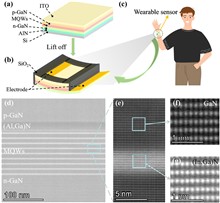
Because of extensive potential applications in health fields, wearable self-driven sensors are indispensable for next-generation medical systems. In this paper, a wearable self-driven sensor utilizing a lift-off (In,Ga)N film is proposed and demonstrated successfully. (In,Ga)N film is separated from an epitaxial silicon substrate through an economical and fast electrochemical etching procedure. With good flexibility, the self-driven sensor can continuously monitor localized sweat and sweat electrolyte concentrations. Hence, it can monitor the electrolyte loss in the human body, which is crucial to facilitate proper fluid replenishment for people during exercise. Furthermore, the sensor maintains stable detection performance under different bending conditions, indicating good stability. Therefore, this study holds great potential for the advancement of wearable devices for personalized health management requiring ultra-low energy consumption.
Micro-light-emitting diode (micro-LED) has been widely concerned in the field of display and wireless optical communication due to its excellent optoelectronic characteristics, but the reduction of the pixel size has a significant impact on the performance of GaN-based micro-LEDs, which then affects the display and wireless optical communication applications. In this work, different sizes of violet and blue GaN-based micro-LEDs have been successfully fabricated, and the size-dependent characteristics of micro-LEDs in display and communication applications have been systematically studied. It can be found that the pixel size reduction of the micro-LEDs from 80 to 10 µm leads to an obvious decrease in light output power (LOP) by 88.30 % and 44.10 % for blue and violet micro-LEDs, respectively, and a decrease in peak external quantum efficiency (EQE) by 55.14 % and 46.25 % for blue and violet micro-LEDs, respectively. Additionally, micro-LEDs with smaller sizes tend to exhibit a less obvious shift of peak wavelength and smaller broadening of full-width at half-maximum (FWHM) with the increases of current density, showing the potential to achieve a stable display with high quality. Also, the influence of current density on chrominance coordinate migration is determined, which shows that the driving current density corresponding to the maximum EQE can promote display efficiency and color gamut. In addition, the violet and blue micro-LEDs with a diameter of 20 µm show potential in balancing between the LOP and the modulation bandwidth to achieve the highest data rates of 1.347 and 1.032 Gbps, respectively, in wireless optical communication applications. The results of this study are of great significance for optimizing the pixel size of the micro-LED to improve the performance in display and wireless optical communication applications in the future.
The development of artificial synaptic devices that emulate synaptic activity is key to advancing the hardware implementation of neuromorphic computing. In this study, we present an optoelectronic synaptic device based on a NaNbO3/n-GaN heterostructure, which exhibits defect-dominated carrier transport behaviors. This device effectively demonstrates typical synaptic functions, including paired-pulse facilitation, short-term memory, long-term memory, human cognitive behavior, and human visual memory, using both optical and electrical stimuli. These results highlight the potential of the NaNbO3/n-GaN heterostructure for future neuromorphic systems.
Infrared (IR) photodetectors (PDs) are crucial for medical imaging, optical communication, security surveillance, remote sensing, and gas identification. In this Letter, we systematically investigated a room temperature IR PD based on two-dimensional b-As0.5P0.5, a relatively unexplored component of b-AsP alloys. We synthesized high-quality b-As0.5P0.5 flakes via the chemical vapor transport (CVT) method with precisely controlled conditions. The fabricated b-As0.5P0.5 PD exhibits excellent photoconductivity, high responsivity, and a fast response in the visible and near-infrared (Vis-NIR) band. It achieves a responsivity of ∼0.209 A·W-1 and a response time of ∼16.6 µs under 1550 nm IR illumination. High-resolution single-pixel point optical imaging and high-speed optical communication were realized by the b-As0.5P0.5 PDs. This study confirms that b-As0.5P0.5 materials are highly promising for advanced IR optoelectronic applications.
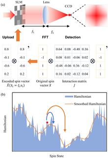
The photonic Ising machine, a promising non-von Neumann computational paradigm, offers a feasible way to address combinatorial optimization problems. We develop a digital noise injection method for spatial photonic Ising machines based on smoothed analysis, where noise level acts as a parameter that quantifies the smoothness degree. Through experiments with 20736-node Max-Cut problems, we establish a stable performance within a smoothness degree of 0.04 to 0.07. Digital noise injection results in a 24% performance enhancement, showing a 73% improvement over heuristic Sahni–Gonzales (SG) algorithms. Furthermore, to address noise-induced instability concerns, we propose an optoelectronic co-optimization method for a more streamlined smoothing method with strong stability.
Facing escalating demands for high-speed, large-bandwidth, and low-latency wireless data links, laser communication technology has emerged as a promising technology. While free-space optical communication conventionally utilizes near-infrared light sources, there has been growing interest in exploring new spectral resources, including visible lasers. Recently, laser-based white light has been demonstrated in visible light communication (VLC), with a unique capability to seamlessly integrate with illumination and display systems. This review summarizes the key devices and system technologies in semiconductor-laser-based white light for VLC-related applications. The recent advances and many emerging applications in the evolution of lighting, display, and communication are discussed.
In this Letter, a kind of optoelectronic chip based on III-nitride is developed as a versatile platform for both fiber-optic sensing and optical communication. The optoelectronic chip consists of a light-emitting diode (LED) and a photodiode (PD), which are fabricated with the same multi-quantum well (MQW) structure and monolithically integrated on a sapphire substrate. By integrating the chip with a polydimethylsiloxane (PDMS) encapsulated silica fiber-optic sensor, it can effectively detect the bending-induced light intensity change and generate the photocurrent to point out the angle changes. Besides, such an optoelectronic chip can also be treated as a transceiver, enabling duplex communication for real-time audio and video transmission. The proposed optoelectronic chip has the advantages of miniaturization, versatility, and ease of massive manufacturing, making it promising in integrated optical sensing and communication (IOSAC) systems.
A 4 × 112 Gb/s hybrid-integrated optical receiver is demonstrated based on the silicon-photonic vertical p-i-n photodetector and silicon–germanium transimpedance amplifier. We propose a photonic-electronic co-design technique to optimize both the device-level and system-level performance, based on the end-to-end equivalent circuit model of the receiver. Continuous-time linear equalization and shunt peaking are employed to enhance the frequency response. Experimental results reveal that the optical-to-electrical 3-dB bandwidth of the receiver is 48 GHz. Clear open NRZ eye diagrams at 56 Gb/s and PAM-4 eye diagrams at 112 Gb/s are achieved without an equalizer in the oscilloscope. The measured bit error rates for 56 Gb/s in NRZ and 112 Gb/s in PAM-4 reach 1 × 10-12 and 2.4 × 10⁻⁴ (KP4-FEC: forward error correction) thresholds under -4 dBm input power, respectively. Furthermore, the proposed receiver boasts a power consumption of approximately 2.2 pJ/bit, indicating an energy efficient solution for data center traffic growth.
The generation of high-power laser pulses using a compact hetero-integrated assembly based on a semiconductor laser with a dual-element composite 2 µm × 100 µm aperture and a compact heterothyristor switch is demonstrated. The achieved peak optical power was 33 W with a pulse duration of 3 ns at a thyristor operating voltage of 55 V. The leading edge of the laser pulse turn-on was 50 ps to a power level of 24.7 W, and the turn-on delay between the elements of the composite aperture was 160 ps.
Using an identical monolithic InGaN/GaN light emitting diode (LED) array as the sensing module and a well-designed data processing module, we demonstrate a small-size concentration sensing prototype. Overlap between the emission and the response spectra of the InGaN/GaN LED makes each pair of LEDs in the arrayed chip form a sensing channel. The changes in liquid concentration can be transformed into variation of photocurrent. The system’s sensing properties are further optimized by varying the position, number of receivers, and packaging reflectors. With methyl orange as a tracer agent, the sensing system’s resolution is 0.286 µmol/L with a linear measurement region below 40 µmol/L.
A novel backside-illuminated double-cliff-layer uni-traveling-carrier (DCL-UTC) photodiode with both high responsivity and ultra-broad bandwidth is designed and demonstrated. A thick absorption layer is adopted for high responsivity, and a depletion region with double cliff layers is proposed to alleviate the space charge effect and maintain overshoot electron velocity under large photocurrents. In addition, inductive coplanar waveguide electrodes are employed to enhance the frequency response performance. The 6-µm-diameter photodiode exhibits a high responsivity of 0.51 A/W and a large 3-dB bandwidth of 102 GHz. A high RF output power of 2.7 dBm is recorded at 100 GHz.
In this review paper, we discuss the properties and applications of photonic computing and analog signal processing. Photonic computational circuits have large operation bandwidth, low power consumption, and fine frequency control, enabling a wide range of application-specific computational techniques that are impossible to implement using traditional electrical and digital hardware alone. These advantages are illustrated in the elegant implementation of optical steganography, the real-time blind separation of signals in the same bandwidth, and the efficient acceleration of artificial neural network inference. The working principles and use of photonic circuits for analog signal processing and neuromorphic computing are reviewed and notable demonstrated applications are highlighted.
Organic–inorganic hybrid perovskite formamidinium lead bromide nanosheet (FAPbBr3 NS) is regarded as a superior substance used to construct optoelectronic devices. However, its uncontrollable stability seriously affects its application in the field of photodetectors. In this paper, FAPbBr3 is combined with cadmium sulfide nanobelt (CdS NB) to construct a hybrid device that greatly improves the stability and performance of the photodetector. The response of the FAPbBr3 NS/CdS NB detector under 490 nm light illumination reaches 5712 A/W, while the response of the FAPbBr3 photodetector under equivalent conditions is only 25.45 A/W. The photocurrent of the FAPbBr3 NS/CdS NB photodetector is nearly 80.25% of the initial device after exposure to air for 60 days. The difference in electric field distribution between the single material device and the composite device is simulated by the finite-difference time-domain method. It shows the advantages of composite devices in photoconductive gain and directly promotes the hybrid device performance. This paper presents a new possibility for high stability, fast response photodetectors.
AlGaN-based light-emitting diodes (LEDs) on offcut substrates enhance radiative emission via forming carrier localization centers in multiple quantum wells (MQWs). This study introduces the carrier transport barrier concept, accessing its impact on the quantum efficiency of LEDs grown on different offcut sapphire substrates. A significantly enhanced internal quantum efficiency (IQE) of 83.1% is obtained from MQWs on the 1° offcut sapphire, almost twice that of the controlled 0.2° offcut sample. Yet, 1° offcut LEDs have higher turn-on voltage and weaker electroluminescence than 0.2° ones. Theoretical calculations demonstrate the existence of a potential barrier on the current path around the step-induced Ga-rich stripes. Ga-rich stripes reduce the turn-on voltage but restrict sufficient driving current, impacting LED performance.
In this Letter, we demonstrate ultraviolet (UV) spot position measurement based on the 4 H-SiC quadrant photodetectors (QPDs). The 4 H-SiC QPD with an 8 mm × 8 mm active area exhibits high uniformity across four quadrants, with a consistent low dark current of ∼18 pA and a responsivity of 0.111 A/W at 275 nm. Based on the QPD, the prototype system shows high positioning capability with a slight inherent nonlinearity. Correspondingly, the measurement error is analyzed and a calibration method utilizing the Boltzmann function is developed for the error correction. Evident improvement in positioning accuracy of the measurement system has been realized, achieving a position resolution of 0.3 µm and a mean positioning error of ∼28.5 µm.
In this paper, we demonstrate nBn InAs/InAsSb type II superlattice (T2SL) photodetectors with AlAsSb as the barrier that targets mid-wavelength infrared (MWIR) detection. To improve operating temperature and suppress dark current, a specific Sb soaking technique was employed to improve the interface abruptness of the superlattice with device passivation using a SiO2 layer. These result in ultralow dark current density of 6.28×10⁻⁶ A/cm2 and 0.31 A/cm2 under -600 mV at 97 K and 297 K, respectively, which is lower than most reported InAs/InAsSb-based MWIR photodetectors. Corresponding resistance area product values of 3.20×10⁴ Ω ·cm2 and 1.32 Ω ·cm2 were obtained at 97 K and 297 K. A peak responsivity of 0.39 A/W with a cutoff wavelength around 5.5 µm and a peak detectivity of 2.1×109 cm·Hz1/2/W were obtained at a high operating temperature up to 237 K.
Radio frequency/microwave-directed energy sources using wide bandgap SiC photoconductive semiconductors have attracted much attention due to their unique advantages of high-power output and multi-parameter adjustable ability. Over the past several years, benefitting from the sustainable innovations in laser technology and the significant progress in materials technology, megawatt-class output power electrical pulses with a flexible frequency in the P and L microwave wavebands have been achieved by photoconductive semiconductor devices. Here, we mainly summarize and review the recent progress of the high-power photonic microwave generation based on the SiC photoconductive semiconductor devices in the linear modulation mode, including the mechanism, system architecture, critical technology, and experimental demonstration of the proposed high-power photonic microwave sources. The outlooks and challenges for the future of multi-channel power synthesis development of higher power photonic microwave using wide bandgap photoconductors are also discussed.
Here, we present a study of the effective piezoelectric constant (e14e) temperature dependence in strained [111]-oriented zinc-blende quantum wells (QWs) embedded within a semiconductor optical amplifier (SOA). We determined e14e using a method that was insensitive to the segregation phenomenon and to the temperature dependence of the bandgap energy, which required neither fitting parameters nor temperature-dependent expressions for energy and out-of-plane effective masses of electrons and heavy holes. An e14e=-0.0534±0.0040 C · m-2 at 23°C was obtained for an SOA with 1.2 nm [111]-oriented strained In0.687Ga0.313As/In0.807Ga0.193As0.304P0.696 QWs. Unlike previously published research, where e14e magnitude increased as temperature rised, we extracted an e14e magnitude that decreased as temperature increased.
In this work, high-stability 4H-SiC avalanche photodiodes (APDs) for ultraviolet (UV) detection at high temperatures are fabricated and investigated. With the temperature increasing from room temperature to 150°C, a very small temperature coefficient of 7.4 mV/°C is achieved for the avalanche breakdown voltage of devices. For the first time, the stability of 4H-SiC APDs is verified based on an accelerated aging test with harsh stress conditions. Three different stress conditions are selected with the temperatures and reverse currents of 175°C/100 µA, 200°C/100 µA, and 200°C/500 µA, respectively. The results show that our 4H-SiC APD exhibits robust high-temperature performance and can even endure more than 120 hours at the harsh aging condition of 200°C/500 µA, which indicates that 4H-SiC APDs are very stable and reliable for applications at high temperatures.
In this paper, high-uniformity 2×64 silicon avalanche photodiode (APD) arrays are reported. Silicon multiple epitaxy technology was used, and the high performance APD arrays based on double-layer epiwafers are achieved for the first time, to the best of our knowledge. A high-uniformity breakdown voltage with a fluctuation of smaller than 3.5 V is obtained for the fabricated APD arrays. The dark currents are below 90 pA for all 128 pixels at unity gain voltage. The pixels in the APD arrays show a gain factor of larger than 300 and a peak responsivity of 0.53 A/W@M = 1 at 850 nm (corresponding to maximum external quantum efficiency of 81%) at room temperature. Quick optical pulse response time was measured, and a corresponding cutoff frequency up to 100 MHz was obtained.
Lommel beams have been potential candidates for optical communication and optical manipulation, due to their adjustable symmetry of transverse intensity distribution and continuously variable orbital angular momentum. However, the wavefront of the Lommel beam is scrambled when it transmits through highly scattering media. Here, we explore the construction of Lommel beams through highly scattering media with a transmission matrix-based point spread function engineering method. Experimentally, various Lommel beams with different parameters were generated through a ZnO scattering layer by use of a digital micromirror device. The construction of Lommel beams under high scattering is expected to benefit the optical applications behind highly scattering media.
To optimize the dark current characteristic and detection efficiency of the 1550 nm weak light signal at room temperature, this work proposes a Ge-on-Si avalanche photodiode (APD) in Geiger mode, which could operate at 300 K. This lateral separate absorption charge multiplication APD shows a low breakdown voltage (Vbr) in Geiger mode of -7.42 V and low dark current of 0.096 nA at unity gain voltage (VGain=1 = -7.03 V). Combined with an RF amplifier module and counter, the detection system demonstrates a low dark count rate (DCR) of 1.1×10⁶ counts per second and high detection efficiency η of 7.8% for 1550 nm weak coherent pulse detection at 300 K. The APD reported in this work weakens the dependence of the weak optical signal recognition on the low environment temperature and makes single-chip integration of the single-photon level detection system possible.
In this paper, we propose a 36-quadrature amplitude modulation (QAM) superposition modulation technique that is featured with uneven symbol probability by nonlinear precoding, named nonlinear coded nonuniform superposition (NCNS) QAM. Its aim is to alleviate the nonlinearity effect caused by high instantaneous power in multi-input single-output (MISO) visible light communication (VLC) system, with an uneven probabilistic-shaped constellation. The transmitter includes two LEDs to send signals independently, and the receiver uses a photo detector to receive the superposed QAM signal. The experiment results show that NCNS has a better robustness against nonlinearity than pulse amplitude modulation 4, approximately gaining a 16% increase in maximum usable peak-to-peak voltage and a 33% enlargement in dynamic range area. It is a simple but effective approach to solve the bandwidth limits related to signal power and hopefully be applied in large power VLC systems such as underwater VLC, or to improve the robustness against power fluctuation.
Linearity is a very important parameter to measure the performance of avalanche photodiodes (APDs) under high input optical power. In this paper, the influence of the absorption layer on the linearity of APDs is carefully studied by using bandgap engineering with the structure model of separated absorption, grading, charge, multiplication, charge, and transit (SAGCMCT). The simulated results show that in the hybrid absorption layer device structure the 1 dB compression point can be improved from -9 dBm to -2.1 dBm by increasing the proportion of the p-type absorption layer. In the device structure with only one absorption layer, increasing the doping level of the absorption layer can also improve the 1 dB compression point from -8.6 dBm to 1.43 dBm at a gain of 10. Therefore, the absorption layer is very critical for the linearity of APDs.
High-performance thin film lithium niobate (LN) electro-optic modulators with low cost are in demand. Based on photolithography and wet etching, we experimentally demonstrate a thin film LN Mach–Zehnder modulator with a 3 dB bandwidth exceeding 110 GHz, which shows the potential of boosting the throughput and reducing cost. The fabricated modulator also exhibits a comparable low half-wave voltage-length product of ∼2.37 V·cm, a high extinction ratio of >23 dB, and the propagation loss of optical waveguides of ∼0.2 dB/cm. Besides, six-level pulse amplitude modulation up to 250 Gb/s is successfully achieved.
We demonstrate GaSb-based interband cascade lasers (ICLs) emitting around 3.65 µm, which exhibit a room-temperature continuous-wave (CW) output power above 100 mW. Cavity-length analysis showed that the laser structure has a low internal loss of 3 cm-1 while maintaining a total internal quantum efficiency greater than one. After 6400 h CW operation at 25°C, the threshold current of the laser increased by 3%, and the output power decreased by 7%, indicating good reliability of the device.
Solar-blind ultraviolet photodetectors (SBPDs) have attracted tremendous attention in the environmental, industrial, military, and biological fields. Aluminum gallium nitride (AlGaN), a kind of representative III-nitride semiconductor, has promising prospects in solar-blind photodetection owing to its tunable wide bandgap and industrial feasibility. Considering the high defect density in the AlGaN epilayer directly grown on a sapphire substrate, employing an AlN/sapphire template turns out to be an effective method to achieve a high-quality AlGaN epilayer, thereby enhancing the SBPD performances. In recent years, a variety of remarkable breakthroughs have been achieved in the SBPDs. In this paper, the progress on photovoltaic AlGaN-based SBPDs is reviewed. First, the basic physical properties of AlGaN are introduced. Then, fabrication methods and defect annihilation of the AlN/sapphire template are discussed. Various photovoltaic SBPDs are further summarized, including Schottky barrier, metal-semiconductor-metal, p-n/p-i-n and avalanche photodiodes. Furthermore, surface modification and photoelectrochemical cell techniques are introduced. Benefitting from the development of fabrication techniques and optoelectronic devices, photovoltaic AlGaN photodiodes exhibit a promising prospect in solar-blind ultraviolet photodetection.
At the mirrors of a laser diode self-mixing interferometer, the output beams carry anti-correlated (i.e., in phase opposition) interferometric signals, whereas the superposed noise fluctuations are (partially) correlated. Therefore, by using an instrumental output of the interferometer as the difference of the two, we double the amplitude of the self-mixing useful signal, while the superposed noise is reduced. To validate the idea, we first calculate the noise reduction by means of a second-quantization model, finding that in a laser diode the signal-to-noise ratio (SNR) can be improved by 8.2 dB, typically. Then, we also carry out an experimental measurement of SNR and find very good agreement with the theoretical result.
Understanding detailed avalanche mechanisms is critical for design optimization of avalanche photodiodes (APDs). In this work, avalanche characteristics and single photon counting performance of 4H-SiC n-i-p and p-i-n APDs are compared. By studying the evolution of breakdown voltage as a function of incident light wavelength, it is confirmed that at the deep ultraviolet (UV) wavelength region the avalanche events in 4H-SiC n-i-p APDs are mainly induced by hole-initiated ionization, while electron-initiated ionization is the main cause of avalanche breakdown in 4H-SiC p-i-n APDs. Meanwhile, at the same dark count rate, the single photon counting efficiency of n-i-p APDs is considerably higher than that of p-i-n APDs. The higher performance of n-i-p APDs can be explained by the larger impact ionization coefficient of holes in 4H-SiC. In addition, this is the first time, to the best of our knowledge, to report single photon detection performance of vertical 4H-SiC n-i-p-n APDs.
We have fabricated the AlGaN solar-blind ultraviolet metal–semiconductor–metal (MSM) photodetectors (PDs) with an Al composition of 0.55. The surface roughness and dislocations of the high-Al-content Al0.55Ga0.45N epitaxial layer are analyzed by atomic force microscopy and transmission electron microscopy, respectively. The device exhibits high spectral responsivity and external quantum efficiency due to the photoconductive gain effect. The current reveals a strong dependence on high temperatures in the range of 4–10 V. Moreover, the Poole–Frenkel emission model and changing space charge regions are employed to explain the carrier transport and photoconductive gain mechanisms for the AlGaN PD, respectively.
The AlGaN-based deep ultraviolet (DUV) light-emitting diode (LED) is an alternative DUV light source to replace traditional mercury-based lamps. However, the state-of-the-art DUV LEDs currently exhibit poor wall-plug efficiency and low light output power, which seriously hinder their commercialization. In this work, we design and report a tunnel-junction-cascaded (TJC) DUV LED, which enables multiple radiative recombinations within the active regions. Therefore, the light output power of the TJC-DUV LEDs is more than doubled compared to the conventional DUV LED. Correspondingly, the wall-plug efficiency of the TJC-DUV LED is also significantly boosted by 25% at 60 mA.
We report a method to reduce the detection delay temperature drift for a single-photon detector based on the avalanche photodiode (SPAD). Both the SPAD and the comparator were temperature stabilized, resulting in an ultra-low temperature drift at 0.01 ps/°C. A stable time deviation as 0.15 ps over 1000 s was realized, while the ambient temperature fluctuated rapidly from 24°C to 44°C. To the best of our knowledge, this is the first report on the ultra-stable delay SPAD detector in the case of rapid increase or decrease of ambient temperature. It is helpful to improve the stability of onboard detectors for optical laser time transfer between ground and space.
We propose an optical tensor core (OTC) architecture for neural network training. The key computational components of the OTC are the arrayed optical dot-product units (DPUs). The homodyne-detection-based DPUs can conduct the essential computational work of neural network training, i.e., matrix-matrix multiplication. Dual-layer waveguide topology is adopted to feed data into these DPUs with ultra-low insertion loss and cross talk. Therefore, the OTC architecture allows a large-scale dot-product array and can be integrated into a photonic chip. The feasibility of the OTC and its effectiveness on neural network training are verified with numerical simulations.
We propose a photonic-assisted single system for measuring the frequency and phase noise of microwave signals in a large spectral range. Both the frequency and phase noise to be measured are extracted from the phase difference between the signal under testing and its replica delayed by a span of fiber and a variable optical delay line (VODL). The system calibration, frequency measurement, and phase noise measurement are performed by adjusting the VODL at different working modes. Accurate frequency and phase noise measurement for microwave signals in a large frequency range from 5 to 50 GHz is experimentally demonstrated.
We demonstrate microwave photonic radar with post-bandwidth synthesis, which can realize target detection with ultra-high range resolution using relatively small-bandwidth radio frequency (RF) frontends. In the proposed radar, two temporal-overlapped linear frequency-modulated (LFM) signals with the same chirp rate and different center frequencies are transmitted. By post-processing the de-chirped echoes in the receiver, a signal equivalent to that de-chirped from an LFM signal with the combined bandwidth is achieved. In a proof-of-concept experiment, two LFM signals with bandwidths of 8.4 GHz are exploited to achieve radar detection with an equivalent bandwidth of 16 GHz, and a range resolution of 1 cm is obtained.
A switchable microwave photonic filter (MPF) using a phase modulator (PM) and a silicon-on-insulator micro-ring resonator (MRR) is proposed and demonstrated. By adjusting the polarization controller between the PM and the MRR, the filtering function of the MPF can be switched between a band-stop filter and a band-pass filter. In a proof-of-concept experiment, an MPF with a rejection ratio of 30 dB (or 15 dB) for the band-stop (or band-pass) response and a frequency tuning range from 9.6 to 20.5 GHz is achieved.
We demonstrate a novel multifunctional radar receiver scheme based on photonic parametric sampling. The working principle of photonic parametric sampling based on four-wave mixing (FWM) process is presented. To experimentally verify the multifunctional feasibility, the scheme is individually implemented to carry out a four-channel phased array radar reception and a dual-band radar reception.
A monolithic integrated ultraviolet-infrared (UV-IR) dual-color photodetector based on graphene/GaN heterojunction was fabricated by vertically integrating a GaN nanowire array on a silicon substrate with monolayer graphene. The device detects UV and IR lights by different mechanisms. The UV detection is accomplished by the forbidden band absorption of GaN, and the IR detection is realized by the free electron absorption of graphene. At peak wavelengths of 360 nm and 1540 nm, the detector has responsivities up to 6.93 A/W and 0.11 A/W, detection efficiencies of 1.23 × 1012 cm·Hz1/2 ·W-1 and 1.88 × 1010 cm·Hz1/2 ·W-1, respectively, and a short response time of less than 3 ms.
All-optical magnetization switching with features of low-power consumption and high writing speed is a promising road map to satisfy the demand for volume data storage. To promote denser and faster magnetic recording technologies, herein, all-optical helicity-dependent switching (AO-HDS) in multi-layer magnetic recording is proposed based on the chromatic aberration of an optical lens (Thorlabs’s N-BK7 plano-convex uncoated lens). The power of the incident beams and the thickness of the multi-layer magnetic recording film are designed carefully. Besides, the uniformity of this multi-layer magnetic recording is optimized. At last, a prototype system of information multiplexing based on this multi-layer magnetic recording technology is constructed as well. Flexible and controllable magnetization reversals in different layers are also demonstrated by tuning the wavelength and helicity of working beams. We believe that such a prototype system can pave the way for increasing the storage density in an effective and low-cost mode.
We investigate a channel-interleaved photonic analog-to-digital conversion (PADC) system’s ability to work stably over a long duration with an optimal driving voltage. The influence of optimum bias point drift of a Mach–Zehnder modulator (MZM)-based photonic switch on this system was analyzed theoretically and experimentally. The feasibility of extracting feedback signals from the PADC system was derived. A high-stability channel-interleaved PADC was constructed by extracting a feedback signal from a parallel demultiplexing module to control the MZM-based photonic switch’s driving voltage. Consequently, the amplitude mismatch between the channels was limited to within 0.3 dB over 12 hours of operation.
We have designed and fabricated zero-bias operational two-element symmetric-connected photodetector arrays (SC-PDAs). The designed SC-PDAs have higher saturation currents, larger RF power, and better frequency responses than the single photodetector (PD) under zero bias. The bias-free SC-PDA with 15 μm diameter of each PD demonstrated a 3 dB bandwidth of 19.4 GHz at 0.5 mA. The RF saturation photocurrent and maximum RF output power of the SC-PDA with 40 μm, 50 μm, and 60 μm diameters under zero bias are over 9.31 mA and ?5.86 dBm at 3 GHz, 14.52 mA and 1.17 dBm at 1 GHz, and 13.72 mA and ?1.76 dBm at 1 GHz, respectively.
In this Letter, we propose the electronic manipulation of localized surface plasmon resonance for active tuning in near-field nanofocusing. We theoretically studied the excited graphene tuning of the nanofocusing field in few-layer graphene (FLG)-based hybrid nanotips. It is revealed that the normalized enhanced electric field can be significantly promoted to more than 300 times. It is also observed that resonant peaks can be unprecedently modified by the electron state of excited graphene that is embedded in the substrate. It shows the possibility of flexible tuning of plasmon resonances via controlling the electron excitation state of graphene for specific advanced near-field nanofocusing applications.
Electromagnetically induced transparency (EIT), a typical quantum interference effect, has been extensively investigated in coherent atomic gases. In recent years, it has been recognized that the plasmonic analog of atomic EIT, called plasmon-induced transparency (PIT), is a fruitful platform for the study of EIT-like propagation and interaction of plasmonic polaritons. Many proposals have been presented for realizing PIT in various metamaterials, which possess many unique characters, including the suppression of absorption of electromagnetic radiation, the reduction of propagation velocity, etc. Especially, nonlinear PIT metamaterials, obtained usually by embedding nonlinear elements into meta-atoms, can be used to acquire an enhanced Kerr effect resulted from the resonant coupling between radiation and the meta-atoms and to actively manipulate structural and dynamical properties of plasmonic metamaterials. In this article, we review recent research progress in nonlinear PIT metamaterials, and elucidate their interesting properties and promising applications. In particular, we give a detailed description on the propagation and interaction of nonlinear plasmonic polaritons in metamaterials via PIT, which are promising for chip-scale applications in information processing and transmission.
The optical saturation characteristics in the germanium-on-silicon (Ge-on-Si) photodetector are studied for the first time, to the best of our knowledge. The relationship between the optical saturation characteristics and the optical field distribution in the Ge layer is illustrated by the simulation. This theory is verified by comparative experiments with single-injection and dual-injection structures. The dual-injection photodetector with a more balanced and uniform optical field distribution has a 13% higher responsivity at low optical power and 74.4% higher saturation current at 1550 nm. At higher optical power, the bandwidth of the dual-injection photodetector is five times larger than that of the single-injection photodetector.
In recent years, the nanostructure for solar cells have attracted considerable attention from scientists as a result of a promising candidate for low cost devices. In this work, quantum dots sensitized solar cells with effective performance based on a co-sensitized CdS/CdSe:Mn2+ (or Cu2+) nanocrystal, which was made by successive ionic layer absorption and reaction, are discussed. The optical, physical, chemical, and photovoltaic properties of quantum dots sensitized solar cells were sensitized to Mn2+ and Cu2+ dopants. Therefore, the short current (JSC) of the quantum dot sensitized solar cells is boosted dramatically from 12.351 mA/cm2 for pure CdSe nanoparticles to 18.990 mA/cm2 for Mn2+ ions and 19.915 mA/cm2 for Cu2+ ions. Actually, metal dopant extended the band gap of pure CdSe nanoparticles, reduced recombination, enhanced the efficiency of devices, and improved the charge transfer and collection. In addition, Mn2+ and Cu2+ dopants rose to the level of the conduction band of pure CdSe nanoparticles, which leads to the reduction of the charge recombination, enhances the light-harvesting efficiency, and improves the charge diffusion and collection. The results also were confirmed by the obtained experimental data of photoluminescence decay and electrochemical impedance spectroscopy.
Based on the hybrid integration technology, an ultra-compact and low cost transmitter optical subassembly module is proposed. Four directly modulated lasers are combined with a coarse wavelength division multiplexer operated at the O-band. The bandwidth for all channels is measured to be approximately 3 GHz. The 112 Gb/s transmission is experimentally demonstrated for a 10 km standard single mode fiber (SSMF), in which an optical isolator is used for avoiding the back-reflected and scattered light to improve the bit error rate (BER) performance. A low BER and clear eye opening are achieved for 10 km transmission.
The optical properties of a three-arm plasmonic nanoantenna with and without broken symmetry were analyzed in detail. For the symmetrical structure, the local electric field can be significantly enhanced and well confined within the feed gap, whilst the extinction spectrum illustrates polarization independence. With broken symmetry, multi-wavelength resonances are observed due to the single dipole resonance and dipole–dipole coupling effect, and wide tunability is also available through minor structural adjustment. Especially when illuminated by a circularly polarized light beam, the extinction and the electric field distribution can be effectively modulated by just varying the incident wavelength.
A new configuration of the confinement structure is utilized to improve optoelectronic performance, including threshold current, ac current gain, optical bandwidth, and optical output power of a single quantum well transistor laser. Considering the drift component in addition to the diffusion term in electron current density, a new continuity equation is developed to analyze the proposed structures. Physical parameters, including electron mobility, recombination lifetime, optical confinement factor, electron capture time, and photon lifetime, are calculated for new structures. Based on solving the continuity equation in separate confinement heterostructures, the threshold current reduces 67%, the optical output power increases 37%, and the 3 dB optical bandwidth increases to 21 GHz (compared to 19.5 GHz in the original structure) when the graded index layers of AlξGa1 ξAs (ξ:0.05→0 in the left side of quantum well, ξ:0→0.02 in the right side of quantum well) are used instead of uniform GaAs in the base region.
We demonstrate a high-speed silicon carrier-depletion Michelson interferometric (MI) modulator with a low on-chip insertion loss of 3 dB. The modulator features a compact size of <1 mm2 and a static high extinction ratio of >30 dB. The Vπ·Lπ of the MI modulator is 0.95–1.26 V·cm under a reverse bias of 1 to 8 V, indicating a high modulation efficiency. Experimental results show that a 4-level pulse amplitude modulation up to 20 Gbaud is achieved with a bit error rate of 6×10 3, and a 30 Gb/s binary phase-shift-keying modulation is realized with an error vector magnitude of 25.8%.
We extensively discuss 25 Gb/s per wavelength capacity in both IEEE and ITU-T standardization to support the increasing bandwidth requirement. In this Letter, we propose to use the optical dispersion compensation technique in an optical line terminal (OLT) combined with a bandwidth-limited electro-absorption modulated laser in an optical network unit to achieve 25 Gb/s capacity for the upstream link. We evaluate the positive and negative dispersion tolerances of 25 Gb/s electrical duo-binary (EDB) and pulse-amplitude modulation (PAM-4) signals. We achieve 39.5 and 31 dB upstream loss budgets for the 25 Gb/s EDB and PAM-4 signals by using 600 and 500 ps/nm optical dispersion compensation in OLT, respectively, both supporting 0–40 km differential reach.
A novel design of a two-channel optical add–drop multiplexer based on a self-rolled-up microtube (SRM) is presented. This design consists of an SRM that has a parabolic lobe-like pattern along the tube’s axial direction, as well as straight silicon waveguides and a 180° waveguide bend. The vertical configuration of the SRM and waveguides is analyzed by the coupled mode theory for achieving the optimum gap. In the critical coupling regime, when the device serves as an optical demultiplexer, the minimum insertion loss is 1.94 dB, and the maximum channel crosstalk is 6.036 dB. Also, as an optical multiplexer, the maximum crosstalk becomes 11.9 dB.
The nonlocal effect on the spontaneous emission of a silver cuboid dimer is investigated using a local analog model. Magnetic as well as electric dipole excitations are introduced to excite different gap modes. The nonlocal response of electric and magnetic modes on various parameters of gap (width and refractive index) are investigated. Unidirectional radiation is achieved by the interaction between electric and magnetic modes in both local and nonlocal models. Compared to local simulations, the resonant wavelength is blue shifted and the spontaneous emission enhancement is weakened in the nonlocal model. The relative shifts of the resonant wavelengths get larger in smaller gaps with a higher refractive index.
Electron leakage still needs to be solved for InGaN-based blue-violet laser diodes (LDs), despite the presence of the electron blocking layer (EBL). To reduce further electron leakage, a new structure of InGaN-based LDs with an InGaN interlayer between the EBL and p-type waveguide layer is designed. The optical and electrical characteristics of these LDs are simulated, and it is found that the adjusted energy band profile in the new structure can improve carrier injection and enhance the effective energy barrier against electron leakage when the In composition of the InGaN interlayer is properly chosen. As a result, the device performances of the LDs are improved.
Tris-(8-hydroxyquinoline)-aluminum (Alq3)–based organic light-emitting diodes with Co electrode are fabricated. The positive magnetic electroluminescence (MEL) and magnetic conductance (MC) are observed in the samples, reaching 4.35% and 1.67% under the field of 42 mT at 50 K, respectively, and the MEL and MC traces can be fitted to non-Lorentzian line shapes. The MEL varies as a function of the Co thickness and reaches the optimal value at 10 nm. The MEL and MC dependence on voltage and temperature is also investigated. The electron-hole pair model and the spin-polarized injection mechanism are used to understand the experimental results.
Short-wave infrared (SWIR) detectors combining AlAs/In0.53Ga0.47As/AlAs double barrier structure (DBS) with In0.53Ga0.47As absorption layer are fabricated by molecular beam epitaxy. By adding a p-charge layer, the dark current density of the detector is lowered by 3 orders of magnitude. The responsivity of the detector is tested at room temperature, which reaches 6000 A/W when the power of the incident light is 0.7 nW. The noise equivalent power (NEP) of the detector at 5 kHz is measured to be 3.77×10 14 W/Hz1/2 at room temperature.
We describe a compact beam splitter based on grating-assisted coupler which consists of Bragg grating sandwiched between two parallel waveguides on the silicon-on-insulator platform. The coupled-mode theory is an important method to analyze waveguide structure. The coupling effect is affected by the grating refractive index perturbation due to the phase mismatch between two waveguides with different widths and refractive indices. The power difference between the transmitting and the reflecting directions in waveguide A is nearly 0 when the Bragg wavelength is 1.3464 μm, the index perturbation is 0.245, the period of grating is 0.2 μm, and the distance of two waveguides is 1 μm. At this time, cross couple neighbor waveguides are significantly suppressed. Beam splitter based on grating-assisted coupler is very useful in integrated optical circuits and photonic network-on-chip.
An asymmetric large optical cavity (LOC) waveguide is designed to raise the output power of the 940 nm laser diode. By optimizing the metal organic chemical vapor deposition growth condition and combining with the electrode fabrication and facet coating, single emitter semiconductor laser diodes of 95 mm strip width and 4 mm cavity length are fabricated. Without any active cooling process, an output power of 13.4 W is reached at 15 A injection current without catastrophic optical mirror damage at room temperature. By introducing the asymmetric LOC waveguide, the far-field test shows that only the transverse fundamental mode is lased with a vertical far-field angle full width of half magnitude of 22o.
An integer coordinate commutation project is advanced which leads the aim angle information form optic–electronic detecting system to aim map orientation system and then to countermine system under the middle precision GPS orientation section. This way can we solve the difficult problem that the warning aims coordinate commutation among many optic–electronic vehicle systems. The aim orientation is realized by neat matrix principle. First, the 12 coordinate systems of optic–electronic detecting vehicle system and laser countermine system are defined. Then, the aim coordinate transform mode is changed from the warning sys-tem to the countermine system. It seems that this mode can satisfy the "360" error request of the two vehicle optic–electronic system aim coordinate leading orientation under the complexion of without regarding to the relatively position and angle of the optic–electronic detecting vehicle and laser countermine vehicle.
Tunneling is studied in two main single-photon avalanche diode (SPAD) topologies, which are n-tub guard ring (NTGR) and p-tub guard ring (PTGR). Device simulation, I-V measurements, and dark count calculations and measurements demonstrate that tunneling is the main source of noise in NTGR, but it is less dominant in PTGR SPADs. All structures are characterized with respect to dark noise, photon detection probability, timing jitter, afterpulsing probability, and breakdown voltage. Noise performance is disturbed because of tunneling, whereas jitter performance is disturbed because of the short diffusion time of photo-generated minority carriers in NTGR SPADs. The maximum photon detection probability is enhanced because of an improvement in absorption thickness.
Wired local network is used widely in a vehicle. It brings the benefits of sharing information and controlling automatically as well as causes negative reaction and a troublesome problem to vehicle such as weight, cost, electromagnetism and space and so on. Infrared optical wireless communications are an alternative way to break through these limitations for increasing safety, decreasing fuel consumption and high bandwidth. In this letter, we address the issue of design a wireless network in a vehicle with an infrared link and ring topology. We discuss the performance requirement of the network, and analyz its bandwidth, power, link distance choice and message schedule. At last, we simulate the preferred parameters of an optical link system.
Thermal atomic layer deposited (ALD) Al2O3 films are applied at the front and rear sides of PERC-type c-Si solar cells. At the front side, Al2O3/SiNx as a double-layer antireflection coating reduces the reflection loss, and at the rear side, Al2O3 film as the passivation layer decreases the surface recombination velocity and enhances the internal reflectance at near-infrared (NIR) band together with SiNx layer. Due to the improvement in the reflectance combined with a decrease of the surface recombination velocity, the PERC solar cells show an improved Jsc by 0.2 mA/cm2 compared with the full-area back surface field cell.
Large-area metallic photonic crystals (MPCs) consist of two-dimensional (2D) periodical arrays of gold nano-holes are fabricated by solution-processible gold nanoparticles using interference lithography in combination with subsequent lift-off and annealing processes. By controlling the annealing temperature, the 2D nano-hole arrays are transformed into nano-island arrays, enabling easy achievements of two different photonic devices. The microscopic characterization shows convincingly the success of the fabrication techniques and verifies our proposed mechanisms for this kind of nanoscale morphology transformation. This kind of mechanisms can be applied extensively in the metallic nanofabrication and in the realization of plasmonic photonic devices.
The relative coupling efficiency of top two-dimensional metal coupling grating for mid-wave quantum well infrared photodetector is calculated by finite difference time domain algorthms. The relative coupling efficiency with respect to the grating parameters, such as grating period, duty ratio, and grating depth, is computed. The calculated results show that the relative coupling efficiency will reach the largest value for the 4.1 μm incident infrared light when taking grating period as 1.3 μm, duty ratio as 0.75, grating depth as 0.4 \mu m.
We fabricate an ultraviolet photodetector based on a blend of poly (N-vinylcarbazole) (PVK) and 2-tert-butylphenyl-5-biphenyl-1,3, 4-oxadiazole (PBD) using spin coating. The device exhibites a low dark current density of 2.2 \times 10?3 \muA/cm2 at zero bias. The spectral response of the device shows a narrow bandpass characteristic from 300 to 355 nm, and the peak response is 18.6 mA/W located at 334 nm with a bias of –1 V. We also study the performances of photodetectors with different blend layer thicknesses. The largest photocurrent density is obtained with a blend of 90 nm at the same voltage.
We design a compact triplexer based on two-dimensional (2D) hexagonal lattice photonic crystals (PCs). A folded directional coupler (FDC) is introduced in the triplexer beside the point-defect micro-cavities and line-defect waveguides. Because of the reflection feedback of the FDC, high channel drop efficiency can be realized and a compact size with the order of micrometers can be maintained. The proposed device is analyzed using the plane wave expansion method, and its transmission characteristics are calculated using the finite-difference time-domain method. The footprint of the triplexer is about 12×9 μm, and its extinction ratios are less than –20 dB for 1310 nm, approximately –20 dB for 1490 nm, and under –40 dB for 1550 nm, making it a potentially essential device in future fiber-to-the-home networks.