


 View fulltext
Advanced Photonics
Co-Editors-in-Chief
Xiao-Cong (Larry) Yuan, Anatoly Zayats

2025
Volume: 7 Issue 6
5 Article(s)
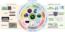
Xiwen He, Zheng Zhang, Deyue Ma, Chen Zhou, Huihuang Hou, Youqiang Shuai, Jiqiao Liu, Rongping Wang, Zhiping Zhou, and Weibiao Chen
Erbium-doped/erbium-ytterbium co-doped waveguide amplifiers (EDWAs/EYCDWAs) have received much attention as essential components within large-scale functionalized silicon-based optoelectronic (SBO) chips for their remarkable ability to amplify optical signals on-chip at the communication band combined with their potential application across diverse fields. We reviewed the research progress of EDWAs/EYCDWAs comprehensively. In particular, the research advancements concerning amplifiers constructed with diverse host materials are introduced in detail, and the gain limitations of the waveguide amplifiers are thoroughly analyzed from multiple perspectives, such as host materials and innovative structural designs. Subsequently, the preparation processes of the gain medium and waveguide structure in EDWAs/EYCDWAs are discussed, and their common application scenarios and commercial applications are summarized. In addition, an assessment is carried out on the challenges encountered by EDWAs/EYCDWAs. Finally, a discussion is held on their potential applications and development prospects in the field of SBO chips, with the aspiration of providing valuable references for the development of EDWAs/EYCDWAs.
Sep. 24, 2025Vol. 7 Issue 6 064001 (2025)
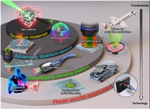
Kihwan Kim, Jong Sung Moon, Dongkwon Lee, Jin Hee Lee, Yuhan Lee, Chanhu Park, Jugyeong Chung, Donghun Lee, and Je-Hyung Kim
Quantum sensing aims to detect signals with unparalleled sensitivity, potentially surpassing classical limitations. Solid-state spin defects, particularly nitrogen-vacancy centers in diamond, have emerged as promising platforms due to their long coherence time, optical addressability, high field sensitivity, and spatial and spectral resolution, making them ideal for sensing and imaging applications. Their compact size and robust performance under room temperature and ambient conditions further enhance their suitability for real-world applications. We provide an overview of quantum sensing principles and explore efforts to improve sensor functionality, including advanced sensing protocols, spatial imaging techniques, and integration with optical systems to enhance detection efficiency. We also highlight recent progress in the applications of these sensors across various use cases, including biomedical diagnostics, semiconductor device inspection, and industrial and military applications.
Sep. 24, 2025Vol. 7 Issue 6 064002 (2025)
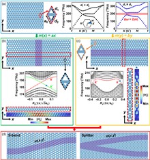
Pan Hu, Lu Sun, Ce Chen, Jingchi Li, Xiong Ni, Xintao He, Jianwen Dong, and Yikai Su
Pseudomagnetic fields (PMFs) can manipulate photons in a similar way that magnetic fields control electrons. However, the PMF-based control over light has been restricted to simple waveguiding of the Landau level states, which hinders the application of PMFs in practical photonic integrated circuits. Here, we propose a universal and systematic methodology to design complex nonuniform PMFs and arbitrarily control the flow of light in silicon photonic crystals at telecommunication wavelengths. As proofs of concept, an S-bend (with a low insertion loss of <1.83 dB) and a 50:50 power splitter (with a low excess loss of <2.11 dB and imbalance of less than ±0.5 dB) based on PMFs are experimentally demonstrated. A high-speed data transmission experiment is performed on these devices with 140-Gb / s four-level pulse amplitude modulation signals to prove their applicability in real communication systems. The proposed method offers a paradigm for exploring magnetic-field-related physics with neutral particles and developing nanophotonic devices with PMF-induced states beyond the Landau level states and the topological edge states.
Sep. 01, 2025Vol. 7 Issue 6 066001 (2025)
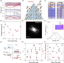
Shafqat Hussain, Shunshun Yang, Shuchao Qin, Yichun Cui, Tong Tong, Xueqian Sun, Kan Zhou, Jian Kang, Le Tang, Han Yan, Jiajie Pei, Haizeng Song, Neng Wan, Jiong Yang, Fei Zhou, Hucheng Song, Youwen Liu, Yuerui Lu, and Linglong Zhang
In two-dimensional (2D) organic–inorganic (O-I) heterostructures, interlayer coupling has emerged as a design parameter for engineering their electronic and optoelectronic properties, essential for designing future excitonic and optoelectronic devices. However, the further exploration of interlayer couplings is limited by their weak strength and ineffective tuning strategies, due to the inconsistent material quality and the bulky size of organic counterparts. Here, we integrate 2D pentacene single crystals with monolayer MoS2 to achieve strong interlayer coupling and effective tuning through a twisting method. We confirm this strong coupling through calculated lower interlayer spacing (∼2.70 Å), high charge transfer efficiency (∼61 % ), and a high coupling strength of ∼2.72 at a twist angle of ∼32 deg. Both density functional theory calculations and experimental results demonstrate the remarkable electrical control over interlayer couplings by adjusting electrical band alignments. This control over interlayer couplings helps to untangle the diffusion of neutral excitons and trions, which have diffusion lengths of ∼1.95 and 0.93 μm, respectively. Our results underscore the significant tunability of interlayer couplings and relaxations within O-I systems via twist angles, offering avenues for developing high-performance vertical transistors, logic devices, photodetectors, and photovoltaic devices.
Sep. 08, 2025Vol. 7 Issue 6 066002 (2025)
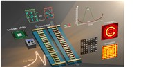
Shuxiang Ma, Yulong Fan, Lin Chen, Chunwang Zhao, Jiandong Sun, Feihu Wang, Dangyuan Lei, Shu Chen, Peng Wang, Yiming Zhu, and Songlin Zhuang
High-quality and real-time holographic imaging based on dynamically tunable metasurfaces has attracted immense interest. Despite remarkable progress, the complex electrical pattern designs and slow-speed near-field scanning terahertz (THz) microscopy systems have significantly hindered the development of real-time electrically tunable metasurface holography in the THz band. We propose and experimentally demonstrate an electrically tunable vanadium dioxide (VO2)-based active metasurface that can generate real-time bias-controlled holographic information via a THz focal plane imaging system. By elaborately designing “microladders” integrated with VO2 pads, the device exhibits low power consumption (∼0.8 W) and real-time imaging (∼4.5 s). The quantitative method is theoretically utilized to investigate the thermal parameters dependent thermodynamics of the “ladder” metasurface based on theoretical analysis with the aid of thermal modelling. The calculated dynamic response time based on the quantitative thermodynamic model agrees well with experimental results. Our study can be used to propel the development of THz electrically tunable metasurfaces for low-power-consumption dynamic, real-time displays, and information encryption, providing crucial insights for future optimization of VO2-based electrothermally tunable holographic metasurfaces.
Sep. 25, 2025Vol. 7 Issue 6 066003 (2025)
© Copyright 2018-2021 | Chinese Laser Press.
All Rights Reserved 沪ICP备15018463号-20