


Please enter the answer below before you can view the full text.
5-1=
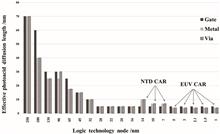
Computational lithography technology plays crucial roles in enhancing resolution. It bridges the gap between chip design and manufacturing processes. In this study, first, rule-based optical proximity correction (OPC) was introduced as the first generation of OPC and the origin of computational lithography. Second, model-based OPC, source mask cooperation, and double patterning technology were introduced under the 14-nm IC manufacturing context. Finally, the trend of computational lithography was discussed and inverse lithography technology, curvilinear masks, AI-based OPCs, and holistic process optimizations were introduced. Integrated optimization of chip design, manufacturing and inspection offers broad prospects for computational lithography.
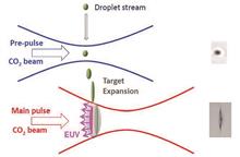
Owing to the continuous reduction in the chip feature size, supported by a 193 nm excimer light source, the deep ultraviolet immersion lithography has reached a bottleneck. The process route using multiple patterning technology has reached the current commercial limit. To address this issue, extreme ultraviolet lithography (EUVL), employing a 13.5 nm extreme ultraviolet light source, has been successfully used in high-volume manufacturing. Thus, it has become an essential technology for the next-generation lithography commercialization. Herein, the principle and latest developments in the 13.5 nm extreme ultraviolet lithography in laser-produced plasma have been reviewed, and the key subsystems, including the driving laser, target, and collecting mirror, have been introduced. Moreover, major challenges that need to be solved in the further development of laser-produced plasma source have been discussed, including the improvement of the driving power and conversion efficiency as well as the prolongation of the light source life. Finally, the EUVL source devices of Japan's Gigaphoton Company and Holland’s ASML Company have been analyzed.
A lithography machine is a key equipment to support the continuous reduction of the size of the integrated circuit. High-performance lithography machine requires high-acceleration and high-precision motion stages. To meet the requirements of the lithography machine, high-performance stage control methods are essential. This paper sorts out and introduces the mainstream control methods of motion stages in the lithography machine. First, the working principle and basic control structure of motion stages are introduced. Then, the control methods of the motion stage are introduced in detail from the aspects of feedforward control, feedback control and over-actuation/over-sensing, to provide a reference for the further development of control methods of lithography machine motion stages.
As Extreme Ultraviolet (EUV) lithography has become the most advanced lithography technology applied in the semiconductor manufacturing industry, corresponding EUV photoresists have also developed significantly in recent years. Herein, the development of polymeric, single-molecule-resin, and organic-inorganic hybrid EUV photoresists has been reviewed, considering the new problems and challenges faced by EUV lithography. It should benefit the researchers in the EUV lithography and photoresist.
Photolithography has been the main driving force for the sustained development of semiconductor integrated circuit technology. Its continuously improved resolution and pattern reproduction accuracy have successfully reduced the manufacturing linewidth of integrated circuit from 2~3 μm more than 40 years ago to the current 10~15 nm. During the course of its evolution, many advanced technologies continue to emerge, such as projection lithography, phase-shifting mask, chemically amplified photoresist, and optical proximity effect correction, which timely ensure the advancement of integrated circuit technology along the prediction of the Moore’s law. This paper uses the history of projection lithography as the clue, from 0.25 μm to today’s 5 nm, to analyze the process requirements and process window of each key technology node, including the added technologies and their respective roles,so as to provide a comprehensive presentation of the photolithography process and related technologies with the purpose to give the readers a professional and technical reference.
Lithography tool is the core equipment for the ultra-large-scale integrated circuit (ULSI) manufacturing. Deep ultraviolet (DUV) lithography tool is the mainstream lithographic equipment in the advanced technology node of chip manufacturing. The imaging quality of lithography tool, which has a direct impact on the performance metrics, is the premise that the lithography tool can work properly. Computational lithography technique is a vital way to improve the lithographic imaging quality when the software and hardware of lithography tool remain unchanged. It optimizes the illumination source, the mask pattern, and the process parameters using mathematical models and algorithms. With the help of computational lithography, the target pattern can be transferred onto the wafer with high imaging fidelity. Lithographic imaging model is the basis of computational lithography technique. The continuous increase of imaging model’s simulation accuracy and speed supports the development of computational lithography technique. Combining the research work of our group, the development of lithographic imaging model is reviewed. Then the research progresses of three main computational lithography techniques, including optical proximity effect correction (OPC), source mask optimization (SMO), and inverse lithography technology (ILT), are summarized in this paper.
Lithography is the process that transfers the structure pattern of integrated circuit device from the mask to the wafer or the surface of other semiconductor substrate, and it is the key technology to implement the mass production of high-end chips. Driven by the Moore’s law, lithography technique has stepped over multiple process nodes from 90 nm to 7 nm and beyond, gradually approaching the physical limit of its resolution. Meanwhile, the lithography image precision is seriously influenced by the diffraction limit property of lithography system, and various system aberrations, errors, and process variations. In this case, the computational lithography techniques must be used to improve the lithography image resolution and fidelity. Computational lithography is a cross research field that involves multiple professional domains, including the optics, semiconductor technology, computing science, image and signal processing, materials science, information science and so on. It is based on the optical imaging and process models, and uses the mathematical methods to simulate and optimize the entire lithography imaging chain, thus realizes the high-precise compensation of the image errors, and is capable of effectively improving the process window and chip manufacturing yield, as well as reducing the research and development cycle and cost of lithography process. To date, it has become one of the core links of the high-end chip manufacturing process. This article first briefly introduces the predecessor of computational lithography, i.e., the traditional resolution enhancement technique, based on which the basic principles, models, and algorithms of computational lithography are introduced. Subsequently, three commonly used computational lithography techniques, including the optical proximity correction, source optimization, and source mask optimization, are reviewed, and the relevant research progress, achievements, and applications are summarized. Finally, this article expounds the current demands and challenges faced by the computational lithography, and discusses the latest technology progress and the future development directions.
Computational lithography is a core technology in manufacturing very large-scale integrated circuits (IC). The requirements for the lithography process are increasing rapidly with a decrease in the IC technology node. Computational lithography technology contributes considerably toward several advancements of the lithography process under the limitation of the hardware technology in lithography tools. The development of computer science provides strong support for computational lithography. However, the balance between speed and accuracy of computational lithography and computational lithography research considering lithography systems, masks, and process errors still require the collaboration of academic and industrial research and development teams. Based on a brief review of important milestones in computational lithography, we focused on an overview of the author team’s research progress in “advanced computational lithography: fast, robustness computational lithography”, including vectorial computational lithography, fast computational lithography, and multiobjective-robustness computational lithography. Finally, we present the future development of computational lithography technology, and hope that this review will help the researchers and engineers in the IC field.
Lithography is the most important equipment in the manufacturing of very large-scale integrated circuits. Resolution is one of the important performance metrics of lithography. As an important means to improve the resolution of lithography, resolution enhancement techniques can promote the development of chips' integration. As one of resolution enhancement techniques, source and mask optimization (SMO) is indispensable in 28 nm technology node and beyond. It improves the resolution by simultaneously optimizing the source and mask. Accurate representation of source and mask is the basis of SMO, and efficient optimization algorithm is the core of SMO. The premise of full chip SMO is critical pattern selection. In this paper, the development history of SMO is reviewed. Combined with the research work of our group, the basic principles and research progress of the critical pattern selection method, source mask representation method, and optimization algorithm are reviewed.
Lithography technology is the core technology of manufacturing integrated circuits. Lithography tools is the core equipment of manufacturing integrated circuits, and illumination system is one of the core components of lithography machine. The working principle of the illumination system of deep ultra-violet step-and-scan projection lithography tools is introduced. The pupil shaping technology, homogenization technology, and polarization illumination technology are reviewed and analyzed. The relevant technical principles and implementation methods are summarized.
One of the most critical elements influencing lithography overlay accuracy is the distortion of the lithography projection objective. The distortion causes transverse magnification of the objective to change with the increase in the field of view, and the pattern exposed on the silicon wafer is displaced relative to its ideal position, which causes overlay errors. During the alignment and use of the objective, distortion must be detected and optimized. At present, the distortion of advanced lithography projection optics is less than 1 nm, and its high-precision measurement is a difficult point in this field. This paper examines the principles and characteristics of three widely used lithography distortion detection technologies-exposure measurement, aerial image measurement, and wavefront measurement-as well as their future development potential. To increase the accuracy and speed of distortion detection, multichannel detection technology is an important development path for lithography nodes of 16‒19 nm and below 16 nm.
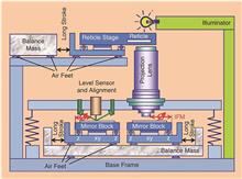
For the step & scan projection lithographic machines, the synchronous servo performance of the reticle and wafer stages will directly affect the technical indexes of the machine. The reticle and wafer stages are typical six degree-of-freedom ultra-precision motion stages. The core control problem is to balance high dynamic and ultra-precision motions under the conditions of coupled dynamics and complex internal and external disturbances. The research and development of ultra-precision motion stage control technology for integrated circuit lithography is of great significance to realize the domestic manufacturing of high-end lithographic machine. This paper first describes the servo performance requirements of ultra-precision motion stages for high-end lithographic machines and the technical challenges to meet these requirements. Then, this paper reviews the research results and recent progress of ultra-precision motion stage control for lithographic machines from five aspects: decoupling control, feedback control, feedforward control, trajectory generation, and cooperative control, and reviews the existing problems and development trends.
Immersion lithography is a crucial technology for the exposure process in the production of high-performance very large-scale integrated circuits with line widths greater than 5 nm. Compared to the traditional dry lithography, the immersion liquid fills the space between the last projective objective and the wafer of immersion lithography. The immersion liquid could improve the numerical aperture and exposure resolution due to its high refractive index; however, it poses a challenge to immersion lithography contamination control. To reduce the exposure defects and increase the manufacturing yield, high-precision detection and the control of various contaminants in the immersion system, i.e., achieving the ultra-clean flow control, must be implemented. This paper discusses the development of immersion lithographic equipment by introducing the principles of immersion lithographic technology and comparing dry and immersion lithography. The focus is on the review of the contaminants for the immersion system of immersion lithography, including their generation mechanism, detection methods, and control techniques. It will serve as a theoretical basis for further improving the chip yield after exposure.
The precision measurement of morphology of wafer by focusing and leveling measurement system is the key to high-quality exposure. The focusing and leveling measurement technology based on optical triangulation is widely used to measure wafer morphology by mainstream lithography manufacturers. In this paper, first, the measurement principle and system composition based on optical triangulation is introduced. Then, aiming at realizing high-precision and high-speed wafer morphology measurement, the key technologies and their evolution process of focusing and leveling measurement system are specially analyzed around the measurement mode, process adaptability and the corresponding imaging optical path. Finally, the improvement and optimization of focusing and leveling measurement system is pointed out in order to meet the requirements of extreme ultra-violet lithography vacuum environment.
Focus control plays important impact on the exposure quality in optical lithography. In order to ensure yield, exposure field needs to be in depth of focus all the time in the exposure process. The relationship between the total defocus of lithography system and yield is discussed by establishing a mathematical model, while the total defocus of lithography is the result of many defocus errors. This paper focuses on the focus control process of advanced dual-stage lithography system and digital micro-mirror device lithography system used for mask manufacturing, then analyzes their main defocus errors. Among the error factors, the focusing and leveling sensor has an important influence on the total defocus, since the focus control of lithography greatly depends on the accurate measurement of the focusing and leveling sensor. In this paper, the focusing and leveling sensors of Canon, Nikon, ASML, etc. are investigated. The working principles and structures of focusing and leveling sensors are compared.
Ultra-precision displacement measurement system is one of the indispensable key subsystems of the lithography machine. The ultra-precision displacement measurement system based on laser heterodyne interference technology has the advantages of sub nano resolution, nano precision, meter range and measurement speed of several meters per second. It is so far the only displacement measurement system that can meet the requirements of the lithography machine. At present, there are two kinds of ultra-precision displacement measurement systems used in lithography: dual frequency laser interferometer and plane grating measurement system, both of which are based on laser heterodyne interference technology. In this paper, the principles, advantages and disadvantages of the two measurement systems and their typical applications in lithography are described.
To meet the ultra-precision and the high-speed displacement measurement requirements of high-end equipments, such as microelectronic lithography machine, the research group from Harbin Institute of Technology has thoroughly explored the traditional heterodyne laser interferometry with coaxial beams and new heterodyne laser interferometry with non-coaxial beams. The group has achieved continuous breakthroughs in many key technologies, including the high-precision laser frequency stabilization, precise suppression of optical nonlinear errors, and high-speed and high-resolution interference signal processing. The group has also developed a series of ultra-precision and high-speed laser interferometers with a vacuum-wavelength relative accuracy up to 9.6 × 10⁻¹⁰, displacement resolution of 0.077 nm, minimum optical nonlinear error of 13 pm, and maximum measuring speed of 5.37 m/s. Currently, these interferometers have been successfully used in integration development and performance test of lithography machine prototypes with nodes ranging from 350 nm to 28 nm and have provided important technical support and measurement methods for high-end equipments in China.
Grating interferometers are becoming important positioning instruments in advanced node lithography machines owing to their high precision and robustness. To meet ultrahighly accurate positioning demands in the worktable of ≤14-nm node lithography machines, homodyne and heterodyne grating interferometry technologies and core systems with multidegree-of-freedom (multi-DOF) and nano/subnanometer metric accuracy were reviewed. Furthermore, a six-DOF positioning system in a current lithography machine enabled by an optimal configuration of “four gratings-four reading heads” was illustrated. Finally, errors in grating interferometers, including environmental error, installation error, and instrument inherent error were briefly discussed, and key challenges in error modeling, separation, and compensation were reviewed for achieving subnanometric accuracy and long-term accuracy stability. Hopefully, this study can provide preliminary guidelines for improving the accuracy and constructing various systems of grating interferometers.
Excimer lasers are widely used in lithography, industrial manufacturing, and medical and scientific fields. Particularly, their indexes such as wavelength, linewidth, energy and dose have great advantages in the field of lithography, therefore can help the lithography machine to obtain smaller image resolution and smoother light exposure. Now excimer lasers have already been used in 7 nm node in semiconductor manufacturing, and are still improving to drive for the lower cost-of-ownership and higher productivity and yield, which promote the development of the whole semiconductor manufacturing industry. Firstly, this paper briefly introduces the principle of excimer lasers, reviews the development history of excimer lasers, investigates the application status of excimer laser in lithography and the mainstream models of foreign excimer lithography light sources, and then focuses on some key technologies of excimer lasers used in lithography. The future trend of applications of excimer lasers in lithography and other links of integrated circuit manufacturing is prospected, which provides a useful reference for the independent and controllable development of excimer lasers in China.
Extreme ultraviolet (EUV) lithography is the most advanced lithography technology, and guarantees the development of the chip to higher integration degree. High imaging quality is the premise to ensure the performance of the EUV lithography system, while the reflective three-dimensional (3D) mask and the special imaging optics bring more challenges in improving the imaging quality of EUV lithography. The research of the imaging of 3D mask is the basis to improve the imaging quality, and the 3D mask imaging model is an important research tool. In this paper, combined with the research work of our group, the principle of the imaging of 3D mask for EUV lithography is briefly introduced and the typical 3D mask models are reviewed. Then the researches on the imaging quality of 3D mask for EUV lithography are introduced. Finally, the research tendency of this field is prospected.
Extreme ultraviolet (EUV) lithographic tool is the core equipment to promote the development of integrated circuits to advanced technology nodes, and has been introduced into high volume manufacturing (HVM) of 7 nm technology node chips and below. High imaging quality is the basis of the application of the EUV lithography for HVM. As an important component of the EUV lithography imaging system, mask is a critical factor that affects the imaging quality. Mask defects, especially multilayer defects, are embedded in the EUV mask during the manufacturing process and result in the degradation of the imaging quality. To assure the imaging quality of EUV lithography, it is important to obtain the location, size, and profile of the mask defect accurately by inspection and compensate for the mask defects according to the information of them. Fast and accurate models for defective mask can help to compensate for the degradation of the imaging quality resulting from the mask defects effectively. In this paper, combining with the research work of our group in the field of mask defect inspection and defect compensation, the typical defective mask simulation methods are introduced, the existing mask inspection techniques are summarized, and the research progress of mask defect compensation techniques are introduced.
Rapidly downsized feature size of lithography process in integrated circuit (IC) manufacturing brings critical demand on smaller overlay error. Correspondingly, overlay metrology and system with a sub-nanometer accuracy are becoming significant requirement. Thus, this study introduces two existing typical measurement techniques, including diffraction-based overlay (DBO) and image-based overlay (IBO), and measurement principles and characteristics of each technology are presented. More intensive review of DBO with higher precision measurement capability is taken, in this part recent progress, challenges, and future works are involved. Hopefully, this study can provide technical references for research and development of home-made advanced lithography machines.
Multilayer piezoelectric actuator has the advantages of small volume, fast response, large stiffness, high displacement accuracy, and large driving force output, which is extensively utilized in the development of lithography scanners. This paper briefly introduces the basic structure and characteristics of multilayer piezoelectric actuator, and lists the typical applications of piezoelectric actuator in high-precision adjustment of projection lens of lithography scanners, positioning of reticle stage, and active vibration isolation of lithography scanners. Finally, the development direction of multilayer piezoelectric actuator is prospected.
Inline measurement and inspection technologies and equipments are the only effective means to ensure manufacturing quality and yield of integrated circuits (IC). It is of great significance to realize fast, nondestructive, and precise measurement and inspection of critical dimension (CD), overlay, defects, and so on, during IC manufacturing. In this paper, we first review the current status of optical measurement and inspection techniques for dimensional metrology and defect inspection in IC manufacturing, including CD and overlay measurement, unpatterned and patterned wafer defect inspection, as well as mask defect inspection. Then, we introduce the potential measurement and inspection challenges in advanced technology nodes, for example, smaller feature sizes and more complex three-dimensional architectures. Finally, we present the perspectives of optical measurement and inspection for future IC manufacturing, including hybrid metrology, ultra-short wavelength metrology, high- and super-resolution imaging, as well as advanced data analytics.
Systems engineering methods have played an important role in the research and development of complex equipment and systems represented by aerospace, defense technology, and ship engineering at home and abroad. For the research and development of advanced semiconductor equipment such as lithography machines, it is particularly important to develop independent innovation and integrated design and manufacturing capabilities led by forward design and guided by systems engineering methods. Starting from the origin of systems engineering, this paper gives a survey of the common methods of systems engineering, and focuses on the related systems engineering tool chains and key technologies of model-based systems engineering with the applications in the field of semiconductor equipment as the background. Finally, this paper looks forward to the application prospects of systems engineering methods, especially model-based systems engineering methods, in domestic semiconductor equipment industry.
To date, advanced patterning techniques lay the foundation of chip manufacturing and the development of modern information technology. With the continues shrinking of dimension of semiconductor devices, it is imperative for us to develop next-generation lithography (NGL) to meet the ever-stringent requirements of advanced technology nodes. Directed self-assembly (DSA), as a novel patterning technique, possesses high throughputs, high resolution, and low processing costs, and has been listed as a promising NGL candidate in the international roadmap for devices and systems. In this paper, we propose the combination of DSA with deep ultraviolet (DUV) lithography, as a potential alternative of extreme ultraviolet (EUV) lithography, to manufacture sub-10 nm microelectronic devices. This hybrid patterning solution is expected to address the key issues related to advanced chip manufacturing in the domestic integrated circuit industry. The potentials of DSA lithography in terms of microphase separation theory of block copolymer, material availability, process flow, compatibility with conventional lithography, cost of ownership, defect density, etc. are critically examined. We also review the latest development of DSA implementation on 300 mm pivot lines. The pioneering work has fully demonstrated the viability of DSA in combination with DUV lithography for very large-scale integration manufacturing. To realize the full benefit of DSA lithography, further development of DSA-aware automatic design and the scalable synthesis of electronic grade polymer materials would be helpful for the establishment of the DSA ecosystem.
Integrated circuit has been invented for more than 60 years, and the pursuit of more powerful performance chips makes the chip manufacturing technology constantly iterate and upgrade. For a long time, chip fabrication methods based on the ultraviolet lithographic projection system have been the only option for large-scale integrated chip fabrication. However, with the extremely ultraviolet lithography applied into the production line and optimized performance, chip manufacturing is advanced to the 7 nm and the following node. Academia and industry are not consensus of whether Moore’s law can last and extremely ultraviolet lithography can support the future chip demand. The next generation of lithography technology route is still undiscovered. Compared with the fifth generation lithography based on extreme ultraviolet projection exposure, this paper proposes the concept of the sixth generation lithographic system based on dual-beam super resolution technology, and discusses the advantages and potential of the sixth generation lithographic system based on dual-beam super resolution technology, and also discusses the difficulties and possible solutions. As an alternative technology different from the ultraviolet lithography technology, the dual-beam super resolution lithography will probably lead the future of chip manufacturing.
The technology and instrument of current photolithography applied in semiconductor industry have been very complex and expensive due to the diffraction limit barrier of linear optics. For achieving nanoscale lithography with visible and near-infrared light, the lithography method is necessary to breaking the diffraction limit. In this article, we introduce the principles and methods of super-diffraction lithography technology, review the progress and current status of laser super-diffraction lithography with problem discussion and prospect of development.
Lithography technology plays an important role in frontier science and national economy and people’s livelihood. With the optimization of optical components such as the exposure light source, digital micromirror device, projection lens and the rapid development of computer control technology, maskless lithography technology based on digital micromirror devices may go hand in hand with the existing well-developed masked lithography technology in the near future, and it will be quite indispensable in certain application fields. In this paper, we introduce the exposure principle, system composition and development history of optical projection lithography based on digital micromirror devices in detail, and we emphasize the strategy for improving the projection lithography resolution as well as achieving ultrafine structures by breaking the optical diffraction limit. Meanwhile, we put forward the unique advantages of projection maskless exposure technology based on digital micromirror devices in achieving micro devices including photonics devices, biological scaffolds and bionic structures, especially its potential applications in novel processing fields by utilizing ultrafast laser.
Nowadays, the world is inseparable from the information technology (IT), while IT is inseparable from the integrated circuit (IC) semiconductor manufacturing technology, that is, microelectronics technology. The most critical technology in IC semiconductor manufacturing is lithography. Lithography emerged in 1958 when Texas Instruments produced the world’s first planar IC. Over the past short 60 years, the lithography resolution limit has been broken again and again, creating a miracle on earth. As the basis of microelectronics technology, lithography and micro-nanofabrication technologies are the highest accuracy manufacturing techonologies so far. Lithography process sizes range from several hundredmicrons to 10 nanometers. Process methods develop from plate ruler scalpel and camera to electron beam lithography. Light source wavelengths range from optical exposure to extreme ultraviolet exposure. In the development process, integration increases by about ten billion times, while the characteristic dimension has been reduced to about one ten-thousandth of the original value. With the rapid development of IC, lithography has also moved from the era of equivalent Moore into the post-Moore era.