


 View fulltext

2023
Volume: 50 Issue 3
10 Article(s)

Rui Chen, Jincheng Wang, Wenzhuo Zhang, Dongsheng Ji, Xinning Zhu, Tao Luo, Jing Wang, and Wei Zhou
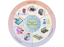
Microstructure sensor is a sensor device with the micro-scale structure as a sensitive unit and can convert external physical, chemical, and biological signals into electrical signals. It has been widely used in intelligent robots, health monitoring, virtual electronics, and other fields. At present, the manufacturing methods of microstructure sensors mainly include laser manufacturing technology, MEMS technology, and 3D printing technology. Laser manufacturing technology is a green processing method that focuses the high-energy laser beam on the object to be processed and makes the laser interact with the material, mainly including laser ablation, laser direct writing, laser induction, and laser-template composite processing. It has the advantages of non-contact processing, no mask, and customizable manufacturing. By optimizing the parameters of the laser manufacturing process, it can realize the efficient and low-cost manufacturing of microstructures with different sizes and shapes. In this paper, the types, function, and manufacturing technology of the microstructures are summarized. At the same time, the microstructure sensors fabricated by laser manufacturing technology are summarized and classified, and the manufacturing technology and application of bioelectric sensors, temperature sensors and pressure sensors are analyzed in detail. Finally, the development trends of the laser manufacturing technology for microstructure sensors are summarized and prospected.
Mar. 25, 2023Vol. 50 Issue 3 220041 (2023)
Yuanyuan Zhao, Feng Jin, Xianzi Dong, Meiling Zheng, and Xuanming Duan
Femtosecond laser two-photon polymerization (TPP) micro-nano fabrication technology, as an important method for the preparation of three-dimensional (3D) micro-nanostructures, has become a hot spot of international frontier research. Using the two-photon absorption effect and the threshold effect of the interaction between laser and matter, this technology can break through the diffraction limit of classical optical theory and achieve nanoscale laser fabrication resolution. It is expected to play an important role in the field of 3D functional micro-nano device fabrication. In this paper, the basic principles of photophysical and photochemical processes in femtosecond pulsed laser TPP fabrication technology will be described, and the research progress and development of this technology in improving line width and fabrication resolution, and improving fabrication efficiency will be reviewed. Then, using the high spatial resolution and true 3D fabrication characteristics of femtosecond laser TPP micro-nano fabrication technology, the researchers prepared various micro-optical devices, integrated optical devices, micro-electromechanical systems, and biomedical devices, fully demonstrating the application prospect of this technology. Finally, how to achieve high-precision, high-efficiency, low-cost, large-area, multi-functional materials and microstructure fabrication, as well as existing challenges and future development directions are discussed and prospected.
Mar. 25, 2023Vol. 50 Issue 3 220048 (2023)
Bin Dong, Juan Zhang, Dawei Wang, Yiyuan Zhang, Leran Zhang, Rui Li, Chen Xin, Shunli Liu, Zihang Zhang, Hao Wu, Shaojun Jiang, Suwan Zhu, Bingrui Liu, and Dong Wu
Miniaturization, integration, and flexible deformation are the future development trends of optical devices. Meanwhile, optical systems based on integrated micro-optical devices stand out for their low power consumption, fast response, and high information storage capacity. However, current high-precision micro/nano processing methods, such as FIB (Focused Ion Beam) and semiconductor lithography, are far too complex and in lack of flexibility. Femtosecond laser, as a non-contact, high-precision, high-intensity tool for "cold" processing, is particularly favored in micro/nano processing. This review first elucidated the background and mechanism of femtosecond laser micromachining used in optical device. After that, we discussed a number of methods employed to improve the resolution of femtosecond micromachining. Then we listed various advanced processing means based on femtosecond laser and systematically summarized recent representative research developments of femtosecond laser micromachining used in microlens, gratings, optical waveguides, and photonic crystals. Finally, we concluded the challenges and the directions for further development of femtosecond laser machining in the field of micro-optical devices.
Mar. 25, 2023Vol. 50 Issue 3 220073 (2023)
Shunhua Yang, Chenliang Ding, Dazhao Zhu, Zhenyao Yang, Yong Liu, Cuifang Kuang, and Xu Liu
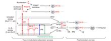
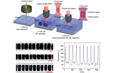
Two-photon polymerization (TPP) based on femtosecond laser has been a research hotspot in 3D micro/nano writing technology. With the increasing demand for processing complex and large-scale miniaturized 3D devices in the fields of life science, material engineering, micro and nano optics, and etc., the issue of low processing efficiency of TPP is becoming increasingly serious. During the long fabrication period, many disturbances can be introduced in the processing, causing the quality deterioration of the structure and seriously hindering the further popularization and application of these crucial 3D devices. This paper respectively compares the four approaches of single-beam writing, parallel multi-beam writing, pattern projection, and 3D projection exposure based on the TPP lithography efficiency. Moreover, the researches on the optical design of system, the writing accuracy, the fabrication throughput, the writing strategy, and etc. of each approach are also described. And the advantages and disadvantages of these four methods are summerized simultaneously. Finally, we also made a brief prospect to the developing trend of TPL efficiency improvement in the future.
Mar. 25, 2023Vol. 50 Issue 3 220133 (2023)
Zhixiang Chen, Quanxin Yang, and Hongliang Liu
In this paper, we propose a femtosecond laser-induced surface periodic structure (LIPSS) based on relaxed ferroelectric PMN-PT crystals. By changing the applied laser parameters, the period of the LIPSS structure is varied from 750 nm to 3 μm. Finally, the phase transition properties of the LIPSS structure are investigated by increasing the temperature. Compared to the phase transition properties of the substrate, the Curie temperature of the LIPSS structure is significantly reduced, and this will provide a possible new idea for the preparation of temperature-controlled modulators based on PMN-PT crystals.
Mar. 25, 2023Vol. 50 Issue 3 220275 (2023)
Shuai Du, Chenglin Zhang, Wenming Sun, Yuping Ma, and Yansheng Yao
Laser microfabrication has the characteristics of ultra fast, ultra precision, etc. It has unique advantages in the field of medical equipment by contrast with traditional processing technology. Especially, it plays an irreplaceable role in the surface processing of biological materials to improve the biocompatibility of materials. The latest application of laser microfabrication in the field of medical equipment manufacturing and processing in recent years is reviewed. The structure and surface manufacturing of vascular stents and bone stents, and the surface modification of biomaterials and antibacterial treatment are emphatically introduced. Finally, the limitations of the current laser micromachining technology are discussed, and the application and development of laser micromachining technology in medical equipment in the future are prospected.
Mar. 25, 2023Vol. 50 Issue 3 220306 (2023)

Zhidong Yin, Caiding Ni, Sizhu Wu, and Zhaoxin Lao
Surface-enhanced Raman spectroscopy (SERS) technique plays an important role in molecular recognition fields due to its highly sensitive and high-resolution. As an emerging low-cost, high machining accuracy, and high-flexibility processing method, femtosecond laser direct writing processing has been widely used in the field of preparing SERS substrates. This work introduces four methods of preparing SERS substrates by femtosecond laser direct writing, including femtosecond two-photon reduction, femtosecond laser cutting metal, femtosecond laser cutting-sputtering, and femtosecond laser 3D printing. The article introduces the performance and application scenarios of each method in preparing SERS substrates and illustrates the advantages of femtosecond laser direct writing processing in preparing SERS substrates, aiming to provide a reference for future related research.
Mar. 25, 2023Vol. 50 Issue 3 220322 (2023)
Chen Zhang, Tong Wen, Zezhi Liu, Wenping Gao, Xinkong Wang, Ziyu Li, Cuifang Kuang, Kaige Wang, and Jintao Bai
Functional surface with specific wettability is one of the indispensable means for droplet manipulation. In recent years, the photo-responsive functional surface with changeable wettability has developed fast. By inducing wetting gradient force, mechanical deformation, phase transformation, dielectric electrophoresis force and electro wettability alteration on the material surface, the behavior of the droplets can be controllably manipulated by the photo-responsive functional surface. In this paper, the development of the photo-responsive functional surface for the droplet manipulation was briefly reviewed. The principles and mechanisms of the droplet manipulation with the functional surface had been expatiated. The categories, structural characteristics and corresponding preparation techniques of the functional surface were analyzed and summarized. In addition, the applications of the photo-responsive functional surface in droplet transportation, fusion, fission, liquid robot, and fluidic chips were introduced in detail. The development tendency and potential applications of the photo-responsive droplet manipulation functional surface were prospected in combination with the characteristics of the functional surface.
Mar. 25, 2023Vol. 50 Issue 3 220326 (2023)
Meiling Luan, Jiaxin Zheng, Xiangchao Sun, and Xueqing Liu
Due to the stable mechanical and chemical properties, excellent photoelectric properties, and other advantages, hard and brittle materials have been widely used in aerospace, the photoelectric industry, and other fields. Laser fabrication is an ideal technology for hard and brittle materials processing due to its high precision, high energy, and non-contact properties. In order to achieve the removal of hard and brittle materials, high laser energy is usually required, resulting in low structural accuracy and poor surface quality. This review introduces the advances of liquid-assisted laser fabrication technology in the processing of hard and brittle materials, introduces the principles of three liquid-assisted laser fabrication technologies, and compares their advantages and disadvantages. The effects of different processing technologies, types of auxiliary liquids, and processing parameters on the quality of different materials were summarized in detail. The main applications of liquid-assisted laser fabrication technology were summarized, and the existing problems and potential development of this technology were discussed.
Mar. 25, 2023Vol. 50 Issue 3 220328 (2023)
Jian Yu, Huan Yang, Jiangen Wu, Yixiang Wu, and Kaichen Xu
Surface-enhanced Raman scattering (SERS) provides important applications in diverse fields. In order to achieve high-precision SERS detection of trace molecules, current research focuses on how to increase the density of hot spots and the number of analyte molecules in the detection area. An ultrafast laser can rapidly construct large-area micro/nano-structures on material surfaces. It is important for the commercial preparation of high-performance SERS sensors. In this paper, the ultrafast laser preparation of high-performance SERS sensors is introduced from the aspect of the density of hot spots and the number of analyte molecules in the detection region. Ultrafast lasers enable both "bottom-up" and "top-down" processing. In particular, the superhydrophobic surface prepared by the ultrafast laser is one of the most effective methods to achieve the enrichment of analyte molecules. Finally, a prospect for the development of laser-prepared SERS substrates is provided.
Mar. 25, 2023Vol. 50 Issue 3 220333 (2023)
© Copyright 2018-2021 | Chinese Laser Press.
All Rights Reserved 沪ICP备15018463号-20