


 View fulltext
Microwave-resonator-enabled broadband on-chip electro-optic frequency comb generation. See Zhaoxi Chen et al., pp. 426.

2025
Volume: 13 Issue 2
32 Article(s)

Fiber Optics and Optical Communications
Jianwei Liu, Ruixuan Wang, Jiyao Yang, Weichao Ma, Henan Zeng, Chenyu Liu, Wen Jiang, Xiangpeng Zhang, Qinyu Xie, and Wangzhe Li
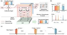
The photonic frequency-interleaving (PFI) technique has shown great potential for broadband signal acquisition, effectively overcoming the challenges of clock jitter and channel mismatch in the conventional time-interleaving paradigm. However, current comb-based PFI schemes have complex system architectures and face challenges in achieving large bandwidth, dense channelization, and flexible reconfigurability simultaneously, which impedes practical applications. In this work, we propose and demonstrate a broadband PFI scheme with high reconfigurability and scalability by exploiting multiple free-running lasers for dense spectral slicing with high crosstalk suppression. A dedicated system model is developed through a comprehensive analysis of the system non-idealities, and a cross-channel signal reconstruction algorithm is developed for distortion-free signal reconstruction, based on precise calibrations of intra- and inter-channel impairments. The system performance is validated through the reception of multi-format broadband signals, both digital and analog, with a detailed evaluation of signal reconstruction quality, achieving inter-channel phase differences of less than 2°. The reconfigurability and scalability of the scheme are demonstrated through a dual-band radar imaging experiment and a three-channel interleaving implementation with a maximum acquisition bandwidth of 4 GHz. To the best of our knowledge, this is the first demonstration of a practical radio-frequency (RF) application enabled by PFI. Our work provides an innovative solution for next-generation software-defined broadband RF receivers.
Jan. 28, 2025Vol. 13 Issue 2 395 (2025)
Holography, Gratings, and Diffraction
Huan Yuan, Wenhao Tang, Zheqiang Zhong, and Bin Zhang
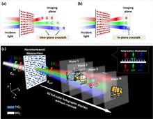
The metasurface possesses great potential in a 3D holographic display due to its powerful ability to manipulate optical fields, ultracompact structure, and extraordinary information capacity. However, the in-plane and interplane crosstalk caused by the coupling between the meta-atoms of the current 3D holographic metasurface limits the quality of the reconstructed image, which has become a significant obstacle to high-performance 3D display applications. Additionally, the interleaved or multilayer design strategy of metasurfaces increases the complexity of structural design and manufacturing, facing challenges in meeting the requirements for miniaturization and low cost-effectiveness. Here, we propose a strategy for a free-space 3D multiplane color holographic multiplex display based on a single-cell metasurface. By utilizing a modified holographic optimization strategy, multiple holographic information is encoded into three mutually independent bases of incident photons and integrated into a metasurface, thereby creating high-quality 3D vectorial metaholography with minimal crosstalk across the visible spectrum. The proposed metasurface has great potential for applications in augmented reality/virtual reality devices, polarization imaging, holographic data encryption, and information storage.
Jan. 07, 2025Vol. 13 Issue 2 235 (2025)
David Blinder, Tobias Birnbaum, and Peter Schelkens
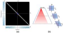
Numerical Fresnel diffraction is broadly used in optics and holography in particular. So far, it has been implemented using convolutional approaches, spatial convolutions, or the fast Fourier transform. We propose a new way, to our knowledge, of computing Fresnel diffraction using Gabor frames and chirplets. Contrary to previous techniques, the algorithm has linear-time complexity, does not exhibit aliasing, does not need zero padding, has no constraints on changing shift/resolution/pixel pitch between source and destination planes, and works at any propagation distance. We provide theoretical and numerical analyses, detail the algorithm, and report simulation results with an accelerated GPU implementation. This algorithm may serve as a basis for more flexible, faster, and memory-efficient computer-generated holography methods.
Jan. 17, 2025Vol. 13 Issue 2 330 (2025)
Yeqi Zhuang, Qiushi Huang, Andrey Sokolov, Stephanie Lemke, Zhengkun Liu, Yue Yu, Igor V. Kozhevnikov, Runze Qi, Zhe Zhang, Zhong Zhang, Jens Viefhaus, and Zhanshan Wang
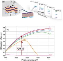
Grating optics lie in the heart of X-ray spectroscopy instruments. The low efficiency and angular dispersion of conventional single-layer-coated gratings significantly limit the transmission and energy resolution of monochromators and spectrometers, particularly in the tender X-ray region (E=1-5 keV). Multilayer-coated blazed gratings (MLBGs) operating at high diffraction orders offer the advantage of achieving both high efficiency and high dispersion simultaneously. Tender X-ray monochromators and spectrometers using different high-order MLBGs have been designed, all demonstrating one to two orders of magnitude higher transmission compared to conventional systems. By employing a 2400 l/mm MLBG at the -4th or -8th diffraction order, the theoretical energy resolution of the instrument is improved by two to three times at 2.5 keV. Two MLBGs operating at the -2nd and -4th orders have been fabricated, showcasing remarkable efficiencies of 34%–12% at 2.5 keV, surpassing that of single-layer-coated gratings by an order of magnitude. Further optimization of manufacturing accuracy can yield even higher efficiencies. The measured angular dispersion agrees well with theoretical predictions, supporting the potential for high resolution. High-order MLBG optics pave the way for a new generation of tender X-ray monochromators/spectrometers that offer both high transmission and high resolution.
Jan. 17, 2025Vol. 13 Issue 2 340 (2025)
Shujun Zheng, Jiaren Tan, Xianmiao Xu, Hongjie Liu, Yi Yang, Xiao Lin, and Xiaodi Tan
Multiplexing technology serves as an effective approach to increase both information storage and transmission capability. However, when exploring multiplexing methods across various dimensions, the polarization dimension encounters limitations stemming from the finite orthogonal combinations. Given that only two mutually orthogonal polarizations are identifiable on the basic Poincaré sphere, this poses a hindrance to polarization modulation. To overcome this challenge, we propose a construction method for the optical polarized orthogonal matrix (OPOM), which is not constrained by the number of orthogonal combinations. Furthermore, we experimentally validate its application in high-dimensional multiplexing of polarization holography. We explore polarization holography technology, capable of recording amplitude, phase, and polarization, for the purpose of recording and selective reconstruction of polarization multi-channels. Our research reveals that, despite identical polarization states, multiple images can be independently manipulated within distinct polarization channels through orthogonal polarization combinations, owing to the orthogonal selectivity among information. By selecting the desired combination of input polarization states, the reconstructed image can be switched with negligible crosstalk. This non-square matrix composed of polarization unit vectors provides prospects for multi-channel information retrieval and dynamic display, with potential applications in optical communication, optical storage, logic devices, anti-counterfeiting, and optical encryption.
Jan. 28, 2025Vol. 13 Issue 2 373 (2025)
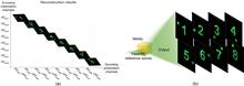
Image Processing and Image Analysis
Wangting Zhou, Zhiyuan Sun, Kezhou Li, Jibao Lv, Zhong Ji, Zhen Yuan, and Xueli Chen
Large-volume photoacoustic microscopy (PAM) or rapid PAM has attracted increasing attention in biomedical applications due to its ability to provide detailed structural and functional information on tumor pathophysiology and the neuroimmune microenvironment. Non-diffracting beams, such as Airy beams, offer extended depth-of-field (DoF), while sparse image reconstruction using deep learning enables image recovery for rapid imaging. However, Airy beams often introduce side-lobe artifacts, and achieving both extended DoF and rapid imaging remains a challenge, hindering PAM’s adoption as a routine large-volume and repeatable monitoring tool. To address these challenges, we developed multitask learning-powered large-volume, rapid photoacoustic microscopy with Airy beams (ML-LR-PAM). This approach integrates advanced software and hardware solutions designed to mitigate side-lobe artifacts and achieve super-resolution reconstruction. Unlike previous methods that neglect the simultaneous optimization of these aspects, our approach bridges this gap by employing scaled dot-product attention mechanism (SDAM) Wasserstein-based CycleGAN (SW-CycleGAN) for artifact reduction and high-resolution, large-volume imaging. We anticipate that ML-LR-PAM, through this integration, will become a standard tool in both biomedical research and clinical practice.
Jan. 31, 2025Vol. 13 Issue 2 488 (2025)

Imaging Systems, Microscopy, and Displays
Vivek Kumar, Pitambar Mukherjee, Lorenzo Valzania, Amaury Badon, Patrick Mounaix, and Sylvain Gigan
Terahertz (THz) microscopy has attracted attention owing to distinctive characteristics of the THz frequency region, particularly non-ionizing photon energy, spectral fingerprint, and transparency to most nonpolar materials. Nevertheless, the well-known Rayleigh diffraction limit imposed on THz waves commonly constrains the resultant imaging resolution to values beyond the millimeter scale, consequently limiting the applicability in numerous emerging applications for chemical sensing and complex media imaging. In this theoretical and numerical work, we address this challenge by introducing, to our knowledge, a new imaging approach based on acquiring high-spatial frequencies by adapting the Fourier synthetic aperture approach to the THz spectral range, thus surpassing the diffraction-limited resolution. Our methodology combines multi-angle THz pulsed illumination with time-resolved field measurements, as enabled by the state-of-the-art time-domain spectroscopy technique. We demonstrate the potential of the approach for hyperspectral THz imaging of semi-transparent samples and show that the technique can reconstruct spatial and temporal features of complex inhomogeneous samples with subwavelength resolution.
Jan. 30, 2025Vol. 13 Issue 2 407 (2025)
Chong Zhang, Xianglei Liu, Lizhi Wang, Shining Ma, Yuanjin Zheng, Yue Liu, Hua Huang, Yongtian Wang, and Weitao Song
Snapshot hyperspectral imaging based on a diffractive optical element (DOE) is increasingly featured in recent progress in deep optics. Despite remarkable advances in spatial and spectral resolutions, the limitations of current photolithography technology have prevented the fabricated DOE from being designed at ideal heights and with high diffraction efficiency, diminishing the effectiveness of coded imaging and reconstruction accuracy in some bands. Here, we propose, to our knowledge, a new lensless efficient snapshot hyperspectral imaging (LESHI) system that utilizes a liquid-crystal-on-silicon spatial light modulator (LCoS-SLM) to replace the traditionally fabricated DOE, resulting in high modulation levels and reconstruction accuracy. Beyond the single-lens imaging model, the system can leverage the switch ability of LCoS-SLM to implement distributed diffractive optics (DDO) imaging and enhance diffraction efficiency across the full visible spectrum. Using the proposed method, we develop a proof-of-concept prototype with an image resolution of 1920×1080 pixels, an effective spatial resolution of 41.74 μm, and a spectral resolution of 10 nm, while improving the average diffraction efficiency from 0.75 to 0.91 over the visible wavelength range (400–700 nm). Additionally, LESHI allows the focal length to be adjusted from 50 mm to 100 mm without the need for additional optical components, providing a cost-effective and time-saving solution for real-time on-site debugging. LESHI is the first imaging modality, to the best of our knowledge, to use dynamic diffractive optics and snapshot hyperspectral imaging, offering a completely new approach to computational spectral imaging and deep optics.
Jan. 31, 2025Vol. 13 Issue 2 511 (2025)
Instrumentation and Measurements
Shuang Liu, Junyi Hu, Binjie Li, Boyi Xue, Wenjie Wan, Huilian Ma, and Zuyuan He
Gyroscopes are crucial components of inertial navigation systems, with ongoing development emphasizing miniaturization and enhanced accuracy. The recent advances in chip-scale optical gyroscopes utilizing integrated optics have attracted considerable attention, demonstrating significant advantages in achieving tactical-grade accuracy. In this paper, a new, to our knowledge, integrated optical gyroscope scheme based on the multi-mode co-detection technology is proposed, which takes the high-Q microcavity as its core sensitive element and uses the multi-mode characteristics of the microcavity to achieve the measurement of rotational angular velocity. This detection scheme breaks the tradition of optical gyroscopes based on a single mode within the sensitive ring to detect the angular rotation rate, which not only greatly simplifies the optical and electrical system of the optical gyroscope, but also has a higher detection accuracy. The gyroscope based on this detection scheme has successfully detected the Earth’s rotation on a 9.2 mm diameter microcavity with a bias instability as low as 1 deg/h, which is the best performance among the chip-scale integrated optical gyroscopes known to us. Moreover, its high dynamic range and highly simplified and reciprocal system architecture greatly enhance the feasibility of practical applications. It is anticipated that these developments will have a profound impact on the field of inertial navigation.
Jan. 17, 2025Vol. 13 Issue 2 319 (2025)
Integrated Optics
Masoud Kheyri, Shuangyou Zhang, Toby Bi, Arghadeep Pal, Hao Zhang, Yaojing Zhang, Abdullah Alabbadi, Haochen Yan, Alekhya Ghosh, Lewis Hill, Pablo Bianucci, Eduard Butzen, Florentina Gannott, Alexander Gumann, Irina Harder, Olga Ohletz, and Pascal Del’Haye
Microresonator dispersion plays a crucial role in shaping the nonlinear dynamics of microcavity solitons. Here, we introduce and validate a method for dispersion engineering through modulating a portion of the inner edge of ring waveguides. We demonstrate that such partial modulation has a broadband effect on the dispersion profile, whereas modulation on the entire resonator’s inner circumference leads to mode splitting primarily affecting one optical mode. The impact of spatial modulation amplitude, period, and number of modulations on the mode splitting profile is also investigated. Through the integration of four modulated sections with different modulation amplitudes and periods, we achieve mode splitting across more than 50 modes over a spectral range exceeding 100 nm in silicon nitride resonators. These results highlight both the simplicity and efficacy of our method in achieving flatter dispersion profiles.
Jan. 17, 2025Vol. 13 Issue 2 367 (2025)
Microwave-resonator-enabled broadband on-chip electro-optic frequency comb generationOn the Cover , Spotlight on Optics
Zhaoxi Chen, Yiwen Zhang, Hanke Feng, Yuansong Zeng, Ke Zhang, and Cheng Wang
Optical frequency combs play a crucial role in optical communications, time-frequency metrology, precise ranging, and sensing. Among various generation schemes, resonant electro-optic combs are particularly attractive for their excellent stability, flexibility, and broad bandwidths. In this approach, an optical pump undergoes multiple electro-optic modulation processes in a high-Q optical resonator, resulting in cascaded spectral sidebands. However, most resonant electro-optic combs to date make use of lumped-capacitor electrodes with relatively inefficient utilization of the input electrical power. This design also reflects most electrical power back to the driving circuits and necessitates costly radio-frequency (RF) isolators in between, presenting substantial challenges in practical applications. To address these issues, we present an RF circuit friendly electro-optic frequency comb generator incorporated with on-chip coplanar microwave resonator electrodes, based on a thin-film lithium niobate platform. Our design achieves more than three times electrical power reduction with minimal reflection at the designed comb repetition rate of ∼25 GHz. We experimentally demonstrate broadband electro-optic frequency comb generation with a comb span of >85 nm at a moderate electrical driving power of 740 mW (28.7 dBm). Our power-efficient and isolator-free electro-optic comb source could offer a compact, low-cost, and simple-to-design solution for applications in spectroscopy, high-precise metrology, and optical communications.
Jan. 30, 2025Vol. 13 Issue 2 426 (2025)
Tianqi Xu, Yushuai Liu, Yuanmao Pu, Yongxiang Yang, Qize Zhong, Xingyan Zhao, Yang Qiu, Yuan Dong, Tao Wu, Shaonan Zheng, and Ting Hu
Scandium-doped aluminum nitride (AlScN) with an asymmetric hexagonal wurtzite structure exhibits enhanced second-order nonlinear and piezoelectric properties compared to aluminum nitride (AlN), while maintaining a relatively large bandgap. It provides a promising platform for photonic circuits and facilitates the seamless integration of passive and active functional devices. Here, we present the design, fabrication, and characterization of Al0.904Sc0.096N electro-optic (EO) micro-ring modulators, introducing active functionalities to the chip-scale AlScN platform. These waveguide-integrated EO modulators utilize sputtered Al0.904Sc0.096N thin films as the light-guiding medium, with the entire fabrication process being compatible with complementary metal-oxide-semiconductor (CMOS) technology. We extract the in-device effective EO coefficient of 2.86 pm/V at 12 GHz. The devices show a minimum half-wave voltage-length product of 3.12 V·cm at a modulation frequency of 14 GHz, and achieve a 3-dB modulation bandwidth of approximately 22 GHz. Our work provides a promising modulation scheme for cost-effective silicon-integrated photonics systems.
Jan. 31, 2025Vol. 13 Issue 2 477 (2025)
Lasers and Laser Optics
Yingjie Lu, Haotian Wang, Jun Guo, Yaohui Xu, Yuanchen Hu, Wujun Li, Jianing Zhang, Jie Ma, and Deyuan Shen
A low-thermal-noise, small-sized, monolithic crystalline whispering-gallery-mode cavity can achieve a compact laser frequency locking system. In this study, we propose generating a Fano resonance spectrum within the crystalline cavity to achieve frequency locking without the need for traditional modulation techniques, aiming to further simplify the locking system. By coupling a prism with the crystalline cavity, we generate a Fano transmission spectrum to serve as the error signal for laser frequency locking. Experimental results show that our method achieves a level of noise suppression comparable to the classical Pound-Drever-Hall technique, reducing laser frequency noise to near the thermal noise limit of the crystalline cavity. It enables us to suppress the laser frequency noise to below 1 Hz2/Hz in the offset frequency range of 103–105 Hz and achieve a minimum noise of 0.2 Hz2/Hz. We also analyzed various unique optical noises in the Fano locking technique and found that the primary factor limiting laser frequency noise in this work is still the inherent thermal noise of the crystalline cavity. Our results indicate that the proposed Fano locking technique has significant potential to simplify laser locking systems, enhance stability, and reduce overall power consumption and cost.
Jan. 30, 2025Vol. 13 Issue 2 417 (2025)
Medical Optics and Biotechnology
Aniwat Juhong, Bo Li, Yifan Liu, Cheng-You Yao, Chia-Wei Yang, A. K. M. Atique Ullah, Kunli Liu, Ryan P. Lewandowski, Jack R. Harkema, Dalen W. Agnew, Yu Leo Lei, Gary D. Luker, Xuefei Huang, Wibool Piyawattanametha, and Zhen Qiu
Imaging of surface-enhanced Raman scattering (SERS) nanoparticles (NPs) has been intensively studied for cancer detection due to its high sensitivity, unconstrained low signal-to-noise ratios, and multiplexing detection capability. Furthermore, conjugating SERS NPs with various biomarkers is straightforward, resulting in numerous successful studies on cancer detection and diagnosis. However, Raman spectroscopy only provides spectral data from an imaging area without co-registered anatomic context. This is not practical and suitable for clinical applications. Here, we propose a custom-made Raman spectrometer with computer-vision-based positional tracking and monocular depth estimation using deep learning (DL) for the visualization of 2D and 3D SERS NPs imaging, respectively. In addition, the SERS NPs used in this study (hyaluronic acid-conjugated SERS NPs) showed clear tumor targeting capabilities (target CD44 typically overexpressed in tumors) by an ex vivo experiment and immunohistochemistry. The combination of Raman spectroscopy, image processing, and SERS molecular imaging, therefore, offers a robust and feasible potential for clinical applications.
Jan. 31, 2025Vol. 13 Issue 2 550 (2025)
Nonlinear Optics
Yaojing Zhang, Shuangyou Zhang, Alekhya Ghosh, Arghadeep Pal, George N. Ghalanos, Toby Bi, Haochen Yan, Hao Zhang, Yongyong Zhuang, Lewis Hill, and Pascal Del’Haye
With the rapid development of the Internet of Things and big data, integrated optical switches are gaining prominence for applications in on-chip optical computing, optical memories, and optical communications. Here, we propose a novel approach for on-chip optical switches by utilizing the nonlinear optical Kerr effect induced spontaneous symmetry breaking (SSB), which leads to two distinct states of counterpropagating light in ring resonators. This technique is based on our first experimental observation of on-chip symmetry breaking in a high-Q (9.4×10⁶) silicon nitride resonator with a measured SSB threshold power of approximately 3.9 mW. We further explore the influence of varying pump powers and frequency detunings on the performance of SSB-induced optical switches. Our work provides insights into the development of new types of photonic data processing devices and provides an innovative approach for the future implementation of on-chip optical memories.
Jan. 17, 2025Vol. 13 Issue 2 360 (2025)
Optical and Photonic Materials
Lei Wang, Cuilian Xu, Jinming Jiang, Mingbao Yan, Zuntian Chu, Huiting Sun, Jun Wang, Sai Sui, Jiafu Wang, Qi Fan, and Yajuan Han
With the rapid development of detection technology and artificial intelligence, the widespread use of multispectral detectors has increased challenges to stealth capabilities. This paper presents a bispectral camouflage metasurface with microwave diffuse emission and tunable infrared (IR) emissivity, achieving an integrated design for radar cross-section (RCS) reduction and tunable IR emissivity. The structure consists of layers from bottom to top: aerogel felt, indium-tin-oxide (ITO), air, polyethylene terephthalate (PET), and ITO. It reduces RCS through microwave diffuse reflection and adjusts IR emissivity by controlling the ITO fill ratio. Both simulations and experiments demonstrate effective suppression of electromagnetic (EM) wave backscattering within 4.5–10.3 GHz, achieving radar invisibility. The tunable IR emissivity ranges from 0.2 to 0.7 with good thermal insulation. This design alleviates issues related to structural thickness and processing complexity and avoids increased thermal load from microwave absorption, offering better tunable IR emissivity for various thermal camouflage environments. This metasurface holds significant promise for multispectral stealth and IR camouflage applications.
Jan. 07, 2025Vol. 13 Issue 2 249 (2025)
Kun Jiang, Xiquan Jiang, Rui Wu, Xinpeng Gao, Shuangshuang Ding, Jingwen Ma, Zhihao Li, and Shuyun Teng
Structural colors with high saturation, large gamut, high resolution, and tunable color are expected in practical applications. This work explores the generation of tunable structural color based on transmission metasurfaces. The designed metasurfaces consist of rectangular nanoholes etched in silver film, which is deposited on the stretchable polydimethylsiloxane (PDMS) substrate. The smaller separation of adjacent nanoholes makes the resolution of metasurface reach 63,500 dpi. The color gamut of the nanostructures reaches 146.9% sRGB. We also perform a comparison with the case on the glass substrate and analyze the incident polarization condition and the coating film of polymethyl methacrylate (PMMA). The ultra-thin structure, high resolution, high-performance structural colors, and convenient transmission mode provide broad application prospects for metasurfaces in color displaying, color printing, and color holographic imaging.
Jan. 07, 2025Vol. 13 Issue 2 257 (2025)
Huiting Sun, Peizhou Hu, Jun Wang, Jingbo Zhao, Ruichao Zhu, Chang Ding, Jie Zhang, Zhaotang Liu, Zuntian Chu, Yina Cui, Fan Wu, Shaobo Qu, and Jiafu Wang
Devices supporting work in multi-physical environments present new challenges for material design. Due to the wavelength difference, waves from multi-field are difficult to modulate simultaneously, limiting the multi-field functions integration. Inspired by characteristic scale analysis, in this work, a devisable metasurface with characteristic scale compatibility is proposed. Under the reduced characteristic scale, waves in microwave, infrared, and acoustic fields can be modulated simultaneously, which can realize the multi-physics functions compatibility. In the microwave field, the far-field performance can be modulated by designing wavefront phase distribution. In the infrared field, the infrared radiation characteristic can be spatially modulated through noninvasive insetting of infrared devices in the microwave layer. In the acoustic field, the sound wave entering the metasurface can realize high-efficiency loss under the action of the Helmholtz cavity. To verify the design method, a functional sample is simulated and experimented. Three typical functions are effectively verified, which can realize 10 dB backward scattering reduction at 8–10 GHz, digital infrared camouflage with infrared emissivity modulation from 0.4 to 0.8 at 3–14 μm, and sound absorptivity of more than 60% at 160–410 Hz, respectively. The comparable characteristic scale design method paves a new way for individually devisable metasurfaces in multi-physical field integration.
Jan. 07, 2025Vol. 13 Issue 2 263 (2025)
Longxing Su, Bingheng Meng, Heng Li, Zhuo Yu, Yuan Zhu, and Rui Chen
All inorganic perovskite CsPbX3 with excellent optical properties and a tunable bandgap is a potential candidate for optoelectronic applications, and the amplified spontaneous emission (ASE) is normally reported in low-dimensional structures where the quantum confinement enhances ASE. Herein, we not only demonstrate the ASE in millimeter size CsPbClxBr3-x crystal with a high defect concentration, but also tune the emission wavelength from the green band to blue band through the ion exchange of Br with Cl. The ASE centered at ∼456 nm is probed at 50 K with a threshold of 106 μJ/cm2. Furthermore, a metal-semiconductor-metal (MSM) structure CsPbClxBr3-x photodetector is fabricated and shows a distinct response to lights from UV to the blue band; the response spectrum range is quite different from the narrow band (∼30 nm) response of the CsPbBr3 photodetector induced by a charge collection narrowing (CCN) mechanism. The CsPbClxBr3-x photodetector also exhibits fast response speeds with a rise time of 96 μs and a decay time of 34 μs, indicating the defects have limited influence on the transportation speed of the photo-generated carriers.
Jan. 09, 2025Vol. 13 Issue 2 286 (2025)
Optical Devices
Jia Shi, Guanlong Wang, Longhuang Tang, Xiang Wang, Shaona Wang, Cuijuan Guo, Hua Bai, Pingjuan Niu, Jianquan Yao, and Jidong Weng
The flexible and precise control of wavefronts of electromagnetic waves has always been a hot issue, and the emergence of metasurfaces has provided a platform to solve this problem, but their design and optimization remain challenging. Here, we demonstrate two design and optimization methods for metagrating-based metalenses based on the highest manipulation efficiency and highest diffraction efficiency. The metalens operating at 0.14 THz with numerical apertures of 0.434 is designed by these two methods for comparison. Then, the metalens is fabricated with photocuring 3D printing technology and an imaging system is built to characterize the distribution of focal spots. With the highest manipulation efficiency, the metalens shows a focal spot with the diameter of 0.93λ and depth of focus (DOF) of 22.7λ, and the manipulation and diffraction efficiencies reach 98.1% and 58.3%. With the highest diffraction efficiency, the metalens shows a focal spot with the diameter of 0.91λ and DOF of 24.6λ, and the manipulation and diffraction efficiencies reach 94.6% and 62.5%. The results show that the metalenses designed by both methods can perform a filamentous focal spot in the sub-wavelength scale with a long DOF; simultaneous high manipulation and diffraction efficiencies are obtained. A transmission imaging manner is used to verify the imaging capability of the metalenses, and the measurements are satisfactorily congruous with the anticipated results. The proposed methods can stably generate focal spots beyond the physical diffraction limit, which has a broad application in terahertz imaging, communications, etc.
Jan. 17, 2025Vol. 13 Issue 2 351 (2025)
Kaicheng Zhang, Jonathon Harwell, Davide Pierangeli, Claudio Conti, and Andrea Di Falco
Optical neural networks (ONNs) are a class of emerging computing platforms that leverage the properties of light to perform ultra-fast computations with ultra-low energy consumption. ONNs often use CCD cameras as the output layer. In this work, we propose the use of perovskite solar cells as a promising alternative to imaging cameras in ONN designs. Solar cells are ubiquitous, versatile, highly customizable, and can be fabricated quickly in laboratories. Their large acquisition area and outstanding efficiency enable them to generate output signals with a large dynamic range without the need for amplification. Here we have experimentally demonstrated the feasibility of using perovskite solar cells for capturing ONN output states, as well as the capability of single-layer random ONNs to achieve excellent performance even with a very limited number of pixels. Our results show that the solar-cell-based ONN setup consistently outperforms the same setup with CCD cameras of the same resolution. These findings highlight the potential of solar-cell-based ONNs as an ideal choice for automated and battery-free edge-computing applications.
Jan. 28, 2025Vol. 13 Issue 2 382 (2025)
Huafeng Dong, Qianxi Yin, Ziqiao Wu, Yufan Ye, Rongxi Li, Ziming Meng, and Jiancai Xue
2D-material-based photodetectors enhanced by plasmonic nanostructures can support responsivity/detectivity several orders higher than commercial photodetectors, drawing extensive attention as promising candidates for the next-generation photodetectors. However, to boost the nanostructure-enhanced 2D photodetectors into real-world applications, crucial challenges lie in the design of broadband enhancing nanostructures and their scalable and position-controllable fabrication. Here, based on a broadband resonant plasmonic disk array fabricated by a scalable and position-controllable technique (direct writing photolithography), we present a visible-near infrared (405–1310 nm) 2D WS2 photodetector, whose detectivity is up to 3.9×10¹⁴ Jones, a value exceeding that of the previous plasmon-enhanced 2D photodetectors. The broadened spectral response range and the high detectivity originate from the hot electron injection, optical absorption enhancement, and strain effect supported by the plasmonic array. Furthermore, the designed plasmonic 2D photodetector supports self-powered photodetection, indicating promising potential in energy-free and portable optoelectronic systems. Our results demonstrate an effective method to construct high-performance broadband photodetectors, which can facilitate the development of 2D photodetectors in commercial applications.
Jan. 30, 2025Vol. 13 Issue 2 453 (2025)
Physical Optics
Jianbo Gao, Xingyuan Lu, Xuechun Zhao, Zhuoyi Wang, Junan Zhu, Zhiquan Hu, Jingjing He, Qiwen Zhan, Yangjian Cai, and Chengliang Zhao
The rotational Doppler effect holds significant potential for remote sensing of rotating objects due to its real-time performance and non-contact advantages. A single-ring beam is used to measure rotation speed. To enhance the signal-to-noise ratio and measure additional parameters, multiple rings are introduced in the context of a rotational Doppler effect. However, the interference between these rings poses a challenge for multitasking detection applications. In this study, cross-polarization superposition was applied to generate an ultra-dense vector perfect vortex beam that exhibited sensitivity to spatial position and object size, and flexibility in designing topological charge combinations for generating frequency combs. A proof-of-principle experiment was conducted to demonstrate its capability in improving the signal-to-noise ratio, and accurately perceiving both the radius of rotation and radial size. An ultra-dense vector perfect vortex beam provides a general strategy for beam construction and the multi-parameter perception of rotating objects, thereby enabling potential applications in the measurement of velocity gradient measurement of fluids.
Jan. 30, 2025Vol. 13 Issue 2 468 (2025)
Dmitrii Tsvetkov, Danilo G. Pires, Hooman Barati Sedeh, and Natalia M. Litchinitser
The rapid development of optical technologies, including optical trapping, enhanced imaging, and microscopy, necessitates fundamentally new approaches to higher-dimensional optical beam shaping. We introduce a rigorous theoretical approach for sculpting three-dimensional, topological particle-like objects, such as optical knots or links, including precise control of their individual parts. Universally applicable to knots created using braided zero lines, our method is validated through theoretical analysis and experimental measurements. The proposed approach enables new degrees of freedom in multi-dimensional singularities shaping, including rotations, shifts, and rescaling of their parts for enhanced stability in complex media. These results may find applications in the fields of three-dimensional optical trapping, manipulation, and subwavelength microscopy, as well as probing and imaging through atmospheric or underwater turbulence.
Jan. 31, 2025Vol. 13 Issue 2 527 (2025)
Quantum Optics
Hongxin Huang, Xiaodi Liu, Yongle Zhou, He Li, and Juntao Li
Solid-state quantum emitters, such as semiconductor quantum dots (QDs), have numerous significant applications in quantum information science. While there has been some success in controlling structured light from kinds of single-photon sources, the simultaneous on-demand, high-quality, and integrated generation of single-photon sources with various degrees of freedom remains a challenge. Here, we utilize composite phase-based metasurfaces, comprising transmission phase and geometric phase elements, to modulate the semiconductor QD emission through a simplified fabrication process. This approach enables to decouple the emission into left and right circularly polarized (LCP/RCP) beams in arbitrary directions (e.g., with zenith angles of 10° and 30°), producing collimated beams with divergence angles less than 6.0° and carrying orbital angular momentum (OAM) modes with different topological charges. Furthermore, we examine the polarization relationship between the output beams and QD emission to validate the performance of our designed devices. Additionally, we achieve eight channels of single-photon emissions, each with well-defined states of spin angular momentum (SAM), OAM, and specific emission directions. Our work not only demonstrates an effective integrated quantum device for the on-demand manipulation of precise direction, collimation, SAM, and various OAM modes, but also significantly advances research efforts in the quantum field related to the generation of multi-OAM single photons.
Jan. 30, 2025Vol. 13 Issue 2 442 (2025)
Silicon Photonics
Zanyun Zhang, Beiju Huang, Qixin Wang, Zilong Chen, Ke Li, Kaixin Zhang, Meixin Li, Hao Jiang, Jiaming Xing, Tianjun Liu, Xiaoqing Lv, and Graham T. Reed
Polarization-insensitive optical modulators allow an external laser to be remotely interconnected by single-mode optical fibers while avoiding polarization controllers, which would be convenient and cost-effective for co-packaged optics, 5G, and future 6G applications. In this article, a polarization-insensitive silicon intensity modulator is proposed and experimentally demonstrated based on two-dimensional centrally symmetric gratings, featuring a low polarization-dependent loss of 0.15 dB in minimum and polarization insensitivity of eye diagrams. The device exhibits a low fiber-to-fiber insertion loss of 9 dB and an electro-optic (EO) bandwidth of 49.8 GHz. A modulation speed of up to 224 Gb/s is also demonstrated.
Jan. 09, 2025Vol. 13 Issue 2 274 (2025)
Qiang Zhang, Qikai Huang, Penghui Xia, Yan Li, Xingyi Jiang, Shuyue Zhang, Shengyu Fang, Jianyi Yang, and Hui Yu
Integrated high-linearity modulators are crucial for high dynamic-range microwave photonic (MWP) systems. Conventional linearization schemes usually involve the fine tuning of radio-frequency (RF) power distribution, which is rather inconvenient for practical applications and can hardly be implemented on the integrated photonics chip. In this paper, we propose an elegant scheme to linearize a silicon-based modulator in which the active tuning of RF power is eliminated. The device consists of two carrier-depletion-based Mach–Zehnder modulators (MZMs), which are connected in series by a 1×2 thermal optical switch (OS). The OS is used to adjust the ratio between the modulation depths of the two sub-MZMs. Under a proper ratio, the complementary third-order intermodulation distortion (IMD3) of the two sub-MZMs can effectively cancel each other out. The measured spurious-free dynamic ranges for IMD3 are 131, 127, 118, 110, and 109 dB·Hz6/7 at frequencies of 1, 10, 20, 30, and 40 GHz, respectively, which represent the highest linearities ever reached by the integrated modulator chips on all available material platforms.
Jan. 30, 2025Vol. 13 Issue 2 433 (2025)
Ying Zhu, Lu Xu, Xin Hua, Kailai Liu, Yifan Liu, Ming Luo, Jia Liu, Ziyue Dang, Ye Liu, Min Liu, Hongguang Zhang, Daigao Chen, Lei Wang, Xi Xiao, and Shaohua Yu
Artificial intelligence (AI), owing to its substantial computing demands, necessitates computing hardware that offers both high speed and high power efficiency. A silicon photonic integrated circuit shows promise as a hardware solution due to its attributes, including high power efficiency, low latency, large bandwidth, and complementary metal–oxide–semiconductor (CMOS) compatibility. Here, we propose a silicon photonic convolution accelerator (SiPh-CA) and experimentally realize a prototype with sub-integrated coherent transmit–receive optical sub-assemblies (sub-IC-TROSAs). The prototype, compared to a previous IC-TROSA-based convolution accelerator, achieves almost the same performances of 1.024 TOPS/channel and 96.22% inference accuracy when it processes neural networks for image recognition, using half the numbers of the modulators and the drivers with which over 1/3 chip footprint and 37.01% power consumption are reduced. By incorporating a broadcasting scheme based on splitters and combiners, the approach can efficiently process multiple convolutions in parallel, achieving several tera operations per second. This scalability feature allows the SiPh-CA to process complex AI and high-performance computing tasks.
Jan. 31, 2025Vol. 13 Issue 2 497 (2025)
Spectroscopy
A. S. Ashik, Peter John Rodrigo, Henning E. Larsen, and Christian Pedersen
We present a differential laser absorption spectroscopy (DLAS) system operating at 1550 nm for rapid and sensitive gas concentration measurements. A dual-wavelength toggling mechanism is presented, which significantly reduces data processing, hence supporting a high update rate and data robustness against fast-changing environmental conditions. We showcase the ability to toggle between two wavelengths separated by 90 pm in 14 μs and with minimal chirp (∼1 pm), facilitating sensitive DLAS measurements at 8 kHz update rate. This performance is achieved by driving a 1550 nm diode laser with a modified square-wave current pulse, overcoming the thermal time constant limited wavelength-modulation response of the diode laser. A sensitive feedback mechanism ensures excellent long-term wavelength stability better than 1.4 pm peak-to-peak at 8 kHz toggling over 20 h. As a performance test, we measured the volumetric ratio (VMR) of hydrogen cyanide (HCN) gas in a fiber-coupled gas cell with less than 0.2% peak-to-peak variation over 20 h at 40 Hz. A best sensitivity in VMR of 8×10⁻⁶ was achieved at 25 ms integration time. The simplicity and high update rate of our system make it well-suited for gas monitoring in dynamic atmospheric and industrial environments. Further, it offers potential utility in applications requiring precise wavelength control, such as injection seeding of pulsed lasers. A simple analytical model is derived, which, in detail, supports the experimental results, hence offering a tool for future design optimization.
Jan. 17, 2025Vol. 13 Issue 2 297 (2025)
Surface Optics and Plasmonics
Hongpei Wang, Lei Ye, Shun Wang, Jiqiang Wang, Menglu Lyu, Liang Qin, Ziyang Zhang, and Cheng Jiang
Owing to the dynamic tunability and strong confinement, graphene plasmons (GPs) have emerged as an excellent candidate for the manipulation of light–matter interaction. Surface plasmons (SPs) have been admitted as another effective way allowing strong confinement of light at the nanoscale. The combination of GPs and SPs like localized surface plasmons (LSPs) and propagating surface plasmon polaritons (SPPs) will lead to a synergistic effect that could remarkably improve light–matter interactions, showing great potential for many applications for the improvement of solar cell efficiency, biosensor sensitivity, and the performance of photonic devices. In this study, the GPs were activated by placing graphene film onto a two-dimensional (2D) phase-changing crystalline Ge2Sb1.5Bi0.5Te5 (cGSBT) nanograting structure, which also acts as an original source generating LSPs. The SPPs originated by laying the above structure onto an Au mirror. The combined effects of GPs, LSPs, and SPPs are epitomized in such a simple Gr/2D cGSBT gratings/Au heterostructure, which allows easy realization of an ultrafast mode-locked laser quite stable working at 1550 nm range due to the strong nonlinear optical absorption capability. This approach overcomes the heat and energy loss in metallic gratings or a Gr-based heterostructure, exhibiting great potential for applications in the design and fabrication of photonic devices.
Jan. 17, 2025Vol. 13 Issue 2 305 (2025)
Borui Wu, Tonghao Liu, Guangming Wang, Xingshuo Cui, Yuxin Jia, Yani Wang, and Huiqing Zhai
With the deepening integration of artificial intelligence (AI) and the Internet of Things (IoT) in daily life, electromagnetic sensing presents both attraction and increasing challenges, especially in the diversification, accuracy, and integration of sensing technologies. The remarkable ability of metasurfaces to manipulate electromagnetic waves offers promising solutions to these challenges. Herein, an integrated system for electromagnetic sensing and beam shaping is proposed. Improved genetic algorithms (GAs) are employed to design the metasurface with desired beams, while spatial electromagnetic signals sensitized by the metasurface are input into the GA enhanced by deep neural networks to sense the number of targets, their azimuths, and elevations. Subsequently, the metasurface device is designed as the hybrid mode combining tracking and avoidance in alignment with practical requirements and sensing outcomes. Simulation and experimental results validate the efficiency and accuracy of each module within the integrated system. Notably, the target sensing module demonstrates the capability to precisely sense more than 10 targets simultaneously, achieving an accuracy exceeding 98% and a minimum angular resolution of 0.5°. Our work opens, to our knowledge, a new avenue for electromagnetic sensing, and has tremendous application potential in smart cities, smart homes, autonomous driving, and secure communication.
Jan. 28, 2025Vol. 13 Issue 2 387 (2025)
M. Simone Soares, Francisco Gameiro, Jan Nedoma, Nuno Santos, Pedro L. Almeida, and Carlos Marques
In the food production sector, quickly identifying potential hazards is crucial due to the resilience of many pathogens, which could lead to wasted production results and, more severely, epidemic outbreaks. E. coli monitoring is essential; however, traditional quality control methods in fish farming are often slow and intrusive, thus promoting an increase in fish stress and mortality rates. This paper presents an alternative method by utilizing a prototype inspired by polarized optical microscopy (POM), constructed with a Raspberry Pi microprocessor to assess pixel patterns and calculate analyte levels. The sensors are based on the immune complexation reactions between E. coli specific antibodies and the disruption of liquid crystal (LC) alignment, which are measured with the POM technique. The prototype yielded a sensitivity of 1.01%±0.17%/log10 (CFU/mL) for E. coli. In this paper, tests using sunlight as the prototype’s light source were also performed, and a user-friendly graphical user interface was designed.
Jan. 31, 2025Vol. 13 Issue 2 541 (2025)
© Copyright 2018-2021 | Chinese Laser Press.
All Rights Reserved 沪ICP备15018463号-20