


Please enter the answer below before you can view the full text.
5-3=
High-performance infrared emitters hold substantial importance in modern engineering and physics. Here, we introduce graphene/PZT (lead zirconate titanate) heterostructure as a new platform for the development of infrared source structure based on an electron–phonon coupling and emitting mechanism. A series of electrical characterizations including carrier mobility [11,361.55 cm2/(V·s)], pulse current (30 ms response time), and cycling stability (2000 cycles) modulated by polarized film was provided. Its maximum working temperature reaches ∼1041 K (∼768°C), and it was broken at 1173 K (∼900°C) within ∼1.2 s rise time and fall time. Based on Wien’s displacement law, the high temperature will lead to near–mid–far thermal infrared when the heterostructure is applied to external voltages, and obvious bright white light could be observed by the naked eye. The changing process has also been recorded by mobile phone. In subsequent infrared emitting applications, 11 V bias voltage was applied on the PZT/graphene structure to produce the temperature change of ∼299 to 445 K within ∼0.96 s rise time and ∼0.98 s fall time. To demonstrate its optical information transmission ability, we exhibited “N, U, C” letters by the time-frequency method at 3 mm×3 mm@20 m condition. Combining with spatial Morse code infrared units, alphabetic information could also be transmitted by infrared array images. Compared with the traditional infrared emitter, the electron–phonon enhancing mechanism and high-performance emission properties of the heterostructure demonstrated a novel and reliable platform for further infrared optical applications.
Advanced technologies such as autonomous driving, cloud computing, Internet of Things, and artificial intelligence have considerably increased data demand. Real-time interactions further drive the development of high-speed, high-capacity networks. Advancements in communication systems depend on developing high-speed optoelectronic devices. Optical communication systems are rapidly evolving, with data rates advancing from 800 Gbps to 1.6 Tbps and beyond, driven by the development of high-performance photodetectors, high-speed modulators, and advanced RF devices. Avalanche photodetectors (APDs) are used in long-distance applications owing to their high internal gain and responsivity. This paper reviews the structural designs of APDs based on various materials for high-speed communication and provides an outlook on developing APDs based on advanced materials.
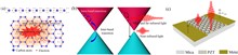
Whispering gallery mode (WGM) resonators have been widely researched for their high-sensitivity sensing capability, but there is currently a lack of high-sensitivity real-time sensing methods for quasi-static measurement. In this paper, within the framework of dissipative coupling sensing, a new method for quasi-static sensing based on the self-modulation of lithium niobate (LiNbO3) resonators is proposed. The LiNbO3 resonator actively modulates the signal to be measured, solving the challenge of real-time demodulation of quasi-static signals. The noise background is upconverted to a high frequency region with lower noise, further enhancing the detection limit. In the demonstration of quasi-static displacement sensing, a customized LiNbO3 resonator with a Q-factor of 2.09×10⁷ serves as the high frequency modulation and sensing element, while the movable resonator acts as the displacement loading unit. Experimental and theoretical results show that the sensing response can be improved to 0.0416 V/nm by dissipation engineering to enhance the resonator evanescent field decay rate and orthogonal polarization optimization. The Allan deviation σ demonstrates a bias instability of 0.205 nm, which represents the best result known to date for microresonator displacement sensing in the quasi-static range. Our proposed scheme demonstrates competitiveness in high-precision quasi-static sensing and provides solutions for the high-precision real-time detection of low frequency or very low frequency acceleration, pressure, nanoparticles, or viruses.
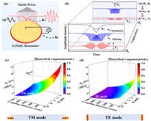
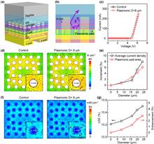
AlGaN-based deep-ultraviolet (DUV) light-emitting diodes (LEDs) still face challenges in achieving high-quality AlGaN material and extracting the strong transverse magnetic (TM) mode emission (which is influenced by valence band splitting inversion). Particularly, these challenges impact devices with wavelengths shorter than 250 nm on their optical power and wall-plug efficiency (WPE) due to an increased proportion of TM mode. Here, the plasmonic omni-directional reflective pad arrays were designed and introduced into the p-contact layer to enhance the light extraction for sub-250 nm DUV LEDs. Meanwhile, a novel device structure, to our knowledge, was put forward, integrating uniformly distributed n-type contact rods as an efficient light guide channel. The theoretical simulation demonstrated a light extraction improvement since these embedded plasmonic reflective pad arrays effectively altered the wavevector of transverse electric (TE) and TM mode photons from the quantum wells. An average enhancement of 12.5% in optical output power was attained in 249.5 nm DUV LEDs through the usage of the optimized diameter of the plasmonic pads. Furthermore, a quartz lens bonded with fluorine resin was introduced to improve refractive index matching at the light output interface, and a high optical power of 3.45 mW was achieved from the original 2.55 mW at a driven current of 100 mA.
Free electron radiation, particularly Smith-Purcell radiation, provides a versatile platform for exploring light-matter interactions and generating light sources. A fundamental characteristic of Smith-Purcell radiation is the monotonic decrease in radiation frequency as the observation angle increases relative to the direction of the free electrons’ motion, akin to the Doppler effect. Here, we demonstrate that this fundamental characteristic can be altered in Smith-Purcell radiation generated by photonic crystals with left-handed properties. Specifically, we have achieved, to our knowledge, a novel phenomenon that the lower-frequency components propagate forward, while the higher-frequency components propagate backward, which we define as reverse Smith-Purcell radiation. Additionally, this reverse Smith-Purcell radiation can confine the radiation to a narrow angular range, which provides a way to obtain broadband light sources in a specific observation angle. Furthermore, by precisely adjusting the grating geometry and the kinetic energy of the free electrons, we can control both the radiation direction and the output frequencies. Our results provide a promising platform to study unexplored light-matter interactions and open avenues to obtain tunable, broadband light sources.
Chaotic dynamics generated by vertical-cavity surface-emitting lasers (VCSELs) has stimulated a variety of applications in secure communication, random key distribution, and chaotic radar for its desirable characteristics. The application of machine learning has made great progress in the prediction of chaotic dynamics. However, the performance is constrained by the training datasets, tedious hyper-parameter optimization, and processing speed. Herein, we propose a heterogeneous forecasting scheme for chaotic dynamics in VCSELs with knowledge-based photonic reservoir computing. An additional imperfect physical model of a VCSEL is introduced into photonic reservoir computing to mitigate the deficiency of the purely data-based approach, which yields improved processing speed, increased accuracy, simplified parameter optimization, and reduced training data size. It is demonstrated that the performance of our proposed scheme is robust to the deficiency of the physical model. Moreover, we elucidate that the performance of knowledge-based photonic reservoir computing will fluctuate with the complexity of chaotic dynamics. Finally, the generality of our results is validated experimentally in parameter spaces of feedback strength and injection strength of reservoir computing. The proposed approach suggests new insights into the prediction of chaotic dynamics of semiconductor lasers.
Flexible quantum dot light-emitting diodes (QLEDs) show great promise for the next generation of flexible, wearable, and artificial intelligence display applications. However, the performance of flexible QLEDs still lags behind that of rigid substrate devices, hindering their commercialization for display applications. Here we report the superior performance of flexible QLEDs based on efficient red ZnCdSe/ZnS/ZnSe QDs (A-QDs) with anti-type-I nanostructures. We reveal that using ZnS as an intermediate shell can effectively confine the exciton wavefunction to the inner core, reducing the surface sensitivity of the QDs and maintaining its excellent emission properties. These flexible QLEDs exhibit a peak external quantum efficiency of 23.0% and a long lifetime of 63,050 h, respectively. The anti-type-I nanostructure of A-QDs in the device simultaneously suppresses defect-induced nonradiative recombination and balances carrier injection, achieving the most excellent performance of flexible QLEDs ever reported. This study provides new insights into achieving superior performance in flexible QD-based electroluminescent devices.
Two-dimensional (2D) graphene has emerged as an excellent partner for solving the scarcity of ultraviolet photodetectors based on three-dimensional (3D) AlGaN, in which the design of a 2D graphene/3D AlGaN junction becomes crucial. This study investigates the response mechanisms of two distinct graphene/AlGaN (Gr-AlGaN) photodetectors in the lateral and vertical configurations. For the lateral Gr-AlGaN photodetector, photogenerated electrons drifting into p-type graphene channel induce negative photoconductivity and a persistent photoconductive effect, resulting in a high responsivity of 1.27×10⁴ A/W and detectivity of 3.88×10¹² Jones. Although the response capability of a vertical Gr-AlGaN device is inferior to the lateral one, it shows significantly reduced dark current and self-powered detection. The photogenerated electron-hole pair can be spontaneously separated by the junction electric field and generate a photocurrent at zero bias. Hence, the vertical Gr-AlGaN photodetector array is satisfied for passive driving imaging like deep space detection. Conversely, the exceptional response of the lateral Gr-AlGaN device emphasizes its prospects for steady object recognition with low-light emission. Moreover, the improved imaging sharpness with light illumination duration makes it suitable for biomimetic visual learning, which follows a recognition to memory process. This study elucidates an efficient approach for diverse photodetection applications through the configuration design of Gr-AlGaN junctions.
The layered two-dimensional material tungsten diselenide (WSe2) has triggered tremendous interests in the field of optoelectronic devices due to its exceptional carrier transport property. Nevertheless, the limited absorption of WSe2 in the near infrared (NIR) band poses a challenge for the application of WSe2 photodetectors in night vision, telecommunication, etc. Herein, the enhanced performance of the WSe2 photodetector is demonstrated through the incorporation of titanium nitride nanoparticles (TiN NPs), complemented by an atomically-thick Al2O3 layer that aids in suppressing the dark current. It is demonstrated that TiN NPs can dramatically enhance the absorption of light in the proposed WSe2 photodetector in the NIR regime. This enhancement boosts photocurrent responses through the generation of plasmonic hot electrons, leading to external quantum efficiency (EQE) enhancement factors of 379.66% at 850 nm and 178.47% at 1550 nm. This work presents, for the first time, to our knowledge, that the WSe2 photodetector is capable of detecting broadband light spanning from ultraviolet to the telecommunication range, all achieved without the reliance on additional semiconductor materials. This achievement opens avenues for the advancement of cost-effective NIR photodetectors.
Neuromorphic applications have shown great promise not only for efficient parallel computing mode to hold certain computational tasks, such as perception and recognition, but also as key biomimetic elements for the intelligent sensory system of next-generation robotics. However, achieving such a biomimetic nociceptor that can adaptively switch operation mode with a stimulation threshold remains a challenge. Through rational design of material properties and device structures, we realized an easily-fabricated, low-energy, and reconfigurable nociceptor. It is capable of threshold-triggered adaptive bi-mode jump that resembles the biological alarm system. With a tunnel silicon nitride (Si3N4) we mimicked the intensity- and rehearsal-triggered jump by means of the tunneling mode transition of Si3N4 dielectric. Under threshold signals the device can also express some common synaptic functions with an extremely low energy density of 33.5 fJ/μm2. In addition, through the modulation of Si3N4 thickness it is relatively easy to fabricate the device with differing pain degree. Our nociceptor analog based on a tunneling layer provides an opportunity for the analog pain alarm system and opens up a new path toward threshold-related novel applications.
Advancements in microwave photonics have yielded novel approaches for generating high-purity microwave sources. Among these, optoelectronic oscillators (OEOs) and coupled optoelectronic oscillators (COEOs) have demonstrated the capability to generate frequency-independent microwaves with exceptionally low phase noise. Nonetheless, the tunability of the oscillators is rather limited due to the necessity for narrowband electronic bandpass filters, presenting challenges in achieving both wide and rapid tuning capabilities. Here, we present a COEO featuring ultralow phase noise, flexible tuning capability, and high robustness. This is achieved through a quiet point (QP)-operated harmonic mode-locked fiber laser, which effectively mitigates optical amplifier noise and supermode competition, thus significantly diminishing the necessity for ultra-narrow electronic filters. Due to the liberated tuning ability, we present an oscillator that can be tuned from 2 GHz to 18 GHz, with phase noise as low as -140 dBc/Hz at 10 kHz under the QP operation. We then illustrate the practical application of the proposed oscillator in generating frequency-hopping signals with consistent spurious modes less than -85 dBc, absolute phase noise below -135 dBc/Hz at 10 kHz, hopping resolution of 1.25 MHz, and fractional frequency stability below 6.1×10⁻¹² at 1 s averaging time when locked to a reference. The presented COEO structure emerges as a compelling solution for agile and low-noise microwave sources in advanced wireless communication and radar systems.
Photonics integration of an optoelectronic oscillator (OEO) on a chip is attractive for fabricating low cost, compact, low power consumption, and highly reliable microwave sources, which has been demonstrated recently in silicon on insulator (SOI) and indium phosphide (InP) platforms at X-band around 8 GHz. Here we demonstrate the first integration of OEOs on the thin film lithium niobate (TFLN) platform, which has the advantages of lower Vπ, no chirp, wider frequency range, and less sensitivity to temperature. We have successfully realized two different OEOs operating at Ka-band, with phase noises even lower than those of the X-band OEOs on SOI and InP platforms. One is a fixed frequency OEO at 30 GHz realized by integrating a Mach–Zehnder modulator (MZM) with an add-drop microring resonator (MRR), and the other is a tunable frequency OEO at 20–35 GHz realized by integrating a phase modulator (PM) with a notch MRR. Our work marks the first step of using TFLN to fabricate integrated OEOs with high frequency, small size, low cost, wide range tunability, and potentially low phase noise.
Visible light communication (VLC) based on laser diodes demonstrates great potential for high data rate maritime, terrestrial, and aerial wireless data links. Here, we design and fabricate high-speed blue laser diodes (LDs) grown on c-plane gallium nitride (GaN) substrate. This was achieved through active region design and miniaturization toward a narrow ridge waveguide, short cavity length, and single longitudinal mode Fabry–Perot laser diode. The fabricated mini-LD has a low threshold current of 31 mA and slope efficiency of 1.02 W/A. A record modulation bandwidth of 5.9 GHz (-3 dB) was measured from the mini-LD. Using the developed mini-LD as a transmitter, the VLC link exhibits a high data transmission rate of 20.06 Gbps adopting the bit and power loading discrete multitone (DMT) modulation technique. The corresponding bit error rate is 0.003, satisfying the forward error correction standard. The demonstrated GaN-based mini-LD has significantly enhanced data transmission rates, paving the path for energy-efficient VLC systems and integrated photonics in the visible regime.
Structured-light (SL) based 3D sensors have been widely used in many fields. Speckle SL is the most widely deployed among all SL sensors due to its light weight, compact size, fast video rate, and low cost. The transmitter (known as the dot projector) consists of a randomly patterned vertical-cavity surface-emitting laser (VCSEL) array multiplicated by a diffractive optical element (DOE) with a fixed repeated pattern. Given that the separation of any two speckles is only one known and fixed number (albeit random), there are no other known scales to calibrate or average. Hence, typical SL sensors require extensive in-factory calibrations, and the depth resolution is limited to 1 mm at ∼60 cm distance. In this paper, to the best of our knowledge, we propose a novel dot projector and a new addressable SL (ASL) 3D sensor by using a regularly spaced, individually addressable VCSEL array, multiplicated by a metasurface-DOE (MDOE) into a random pattern of the array. Dynamically turning on or off the VCSELs in the array provides multiple known distances between neighboring speckles, which is used as a “built-in caliper” to achieve higher accuracy of depth. Serving as a precise “vernier caliper,” the addressable VCSEL array enables fine control over speckle positions and high detection precision. We experimentally demonstrated that the proposed method can result in sub-hundred-micron level precision. This new concept opens new possibilities for applications such as 3D computation, facial recognition, and wearable devices.
Lidar based on the optical phased array (OPA) and frequency-modulated continuous wave (FMCW) technology stands out in automotive applications due to its all-solid-state design, high reliability, and remarkable resistance to interference. However, while FMCW coherent detection enhances the interference resistance capabilities, it concurrently results in a significant increase in depth computation, becoming a primary constraint for improving point cloud density in such perception systems. To address this challenge, this study introduces a lidar solution leveraging the flexible scanning characteristics of OPA. The proposed system categorizes target types within the scene based on RGB images. Subsequently, it performs scans with varying angular resolutions depending on the importance of the targets. Experimental results demonstrate that, compared to traditional scanning methods, the target-adaptive method based on semantic segmentation reduces the number of points to about one-quarter while maintaining the resolution of the primary target area. Conversely, with a similar number of points, the proposed approach increases the point cloud density of the primary target area by about four times.
The photodetectors are critical elements in state-of-the-art technology; however, it is still challenging to realize simultaneously high detectivity and responsivity for the fixed operation mode configuration. In this work, we propose a pn junction local-floating gate photodetector (PNLFG-PD) based on a two-dimensional p-WSe2/n-MoS2 heterojunction, where n-type MoS2 is partly floated on the p-WSe2 channel. The device exhibits the switchable mode between the Λ-shaped anti-ambipolar conduction in dark and the unipolarity conduction of p-type under illumination. Subsequently, the high responsivity of 2.12×10⁵ A/W and detectivity of 1.25×10¹⁴ Jones are simultaneously obtained at 2 V bias and 405 nm illumination of 370 μW light power, resulting in high light/dark ratio over 106 attributed to barrier lowering in the channel. This work provides a particular platform to overcome the tradeoff between detectivity and responsivity for the high-performance photodetection.
Visible–near-infrared (VIS-NIR) dual-mode imaging can expand the human perception limit. However, the development of dual-mode image sensors is still challenging due to complex fabrication processes and readout circuit design. Here, we design a simple-structured (perovskite-Au/Si/Ag) dual-mode photodetector. This unique asymmetric electrode design allows the device to support two operating modes at zero bias. The device exhibits a detection range covering 400–1100 nm under top illumination mode, with a peak specific detectivity of up to 5.56×10¹³ Jones. Under bottom illumination mode, the device demonstrates pronounced narrowband NIR response characteristics. More importantly, we develop a dual-mode single-pixel imaging system based on this device, bypassing the fabrication processes of high-density array image sensors. The system exhibits excellent VIS-NIR dual-mode imaging results, effectively separating NIR and VIS information and enhancing infrared details in the fused images. Interestingly, we discover that the system can effectively suppress ringing artifacts, achieving infrared information perception at a low sampling rate, which can accelerate the imaging speed by ∼16 times (reduced from ∼3.2 s to ∼0.2 s). Our proposed dual-mode single-pixel imaging technology offers new means for material identification and intelligent perception.
Reservoir computing (RC), especially time-delayed RC, as a lightweight, high-speed machine learning paradigm, shows excellent performance in time-series prediction and recognition tasks. Within this framework, time delays play a vital role in dynamic systems, i.e., significantly affecting the transient behavior and the dimensionality of reservoirs. In this work, we explore a multidelay system as the core computational element of RC, which is constructed using a semiconductor laser with photonic-filter feedback. We demonstrate experimentally that the photonic-filter feedback scheme can improve the mapping of scalar inputs into higher-dimensional dynamics, and thus enhance the prediction and classification ability in time series and nonlinear channel equalization tasks. In particular, the rich neural dynamics in turn boosts its memory capacity, which offers great potential for short-term prediction of time series. The numerical results show good qualitative agreement with the experiment. We show that improved RC performance can be achieved by utilizing a small coupling coefficient and eschewing feedback at integer multiples, which can induce detrimental resonance. This work provides an alternative photonic platform to achieve high-performance neural networks based on high-dimensional dynamic systems.
Realization of positive and negative optical responses in a single device promises construction of multifunctional optoelectronic devices. This work demonstrates a Ga2O3/WSe2 mixed-dimensional heterojunction junction field-effect transistor (JFET) with positive and negative photoresponse regulatory functions by gate voltage. The device achieves a remarkable negative responsivity exceeding 425 mA/W. Additionally, benefiting from Fowler-Nordheim tunneling (FNT) behavior, the mixed-dimensional JFET exhibited an excellent negative response performance with response and decay times of 50.1 ms and 53.9 ms and a high IOFF/ION ratio of 343 at Vds=1 V and Vg=5 V under 635 nm illumination. Additionally, the JFET’s negative photoresponse is sensitive to both gate voltage and light intensity, which can be used to realize NAND logic gate and optical communication functions. These results unveil the promising potential of mixed-dimensional optoelectronic devices for optical communication, and logic device technologies.
Terahertz (THz) detectors with high sensitivity, fast response speed, room temperature operation, and self-powered feature are the key component for many THz applications. Microcavity resonators can effectively improve the sensitivity of THz detectors. However, it is difficult to precisely evaluate the microcavity resonator induced such improvement in experiment. Here, we realize a configurable microcavity–antenna-integrated graphene photothermoelectric (PTE) THz detector. Through the microcavity–antenna hybrid structure, THz radiations are localized and enhanced at one end of the graphene channel, and the temperature difference along the channel is greatly increased, resulting in the strong enhancement of PTE response. At the resonant frequency, the device has a high responsivity (976 V/W), low noise equivalent power (2.87 pW/Hz1/2), and fast response speed (300 ns) at room temperature and in zero-bias operation mode. The microcavity-induced peak enhancement factor of 13.14 is accurately extracted. The microcavity–antenna introduced enhancement is further confirmed by using a two-temperature heat transfer model. The strategy of using a configurable microcavity is useful for further optimizing THz detectors by introducing the critical coupling mechanism.
The fiber-optic sensor is a great candidate in the field of metrology, developed to rely on the optical phase to convey valuable information. Some phase amplification methods have attracted wide attention due to their ability to improve measurement sensitivity; nevertheless, the precision is generally restricted in phase measurement. Here, we report a novel optoelectronic hybrid oscillating fiber-optic sensor by mapping the measurand loaded on the sensing fiber to the frequency shift of the microwave signal, which is generated by an all-electric oscillating cavity with a frequency conversion pair. Two branch signals assisted in twice frequency conversion are obtained by heterodyne interference, with the sensing information scaled up by two optical comb line frequencies contained, and then, the phase difference is cumulatively enhanced in the closed feedback loop. Thanks to the introduction of the oscillating cavity, a detection limit improvement of 42 dB at a 10 Hz frequency offset can be achieved in theory with a cavity delay of 1 μs. The sensing precision depends on the cavity noise limit and is independent of the instrument and cavity delay. A proof-of-concept experiment is carried out to demonstrate sensors with a sensitivity of 8.3 kHz/ps and 22.3 kHz/ps for a range of 50 ps, and 62 kHz/ps and 162 kHz/ps for a range of 6.7 ps. The minimum Allan deviation reaches 2.7 attoseconds at an averaging time of 0.2 s with a frequency interval of 150 GHz, indicating that the proposal may pave a new path for sensing interrogation systems, especially for high-precision measurement.
Micro-nano optomechanical accelerometers are widely used in automobile, aerospace, and other industrial applications. Here, we fabricate mechanical sensing components based on an electrically pumped GaN light-emitting diode (LED) with a beam structure. The relationship between the blueshift of the electroluminescence (EL) spectra and the deformation of the GaN beam structure based on the quantum-confined Stark effect (QCSE) of the InGaN quantum well (QW) structure is studied by introducing an extra mass block. Under the equivalent acceleration condition, in addition to the elastic deformation of GaN-LED, a direct relationship exists between the LED’s spectral shift and the acceleration’s magnitude. The extra mass block (gravitational force: 7.55×10⁻¹¹ N) induced blueshift of the EL spectra is obtained and shows driven current dependency. A polymer sphere (PS; gravitational force: 3.427×10⁻¹² N) is placed at the center of the beam GaN-LED, and a blueshift of 0.061 nm is observed in the EL spectrum under the injection current of 0.5 mA. The maximum sensitivity of the acceleration is measured to be 0.02 m/s2, and the maximum measurable acceleration is calculated to be 1.8×10⁶ m/s2. It indicates the simultaneous realization of high sensitivity and a broad acceleration measurement range. This work is significant for several applications, including light force measurement and inertial navigation systems with high integration ability.
Low-intensity light detection necessitates high-responsivity photodetectors. To achieve this, we report In0.53Ga0.47As/InAs/In0.53Ga0.47As quantum well (InAs QW) photo-field-effect-transistors (photo-FETs) integrated on a Si substrate using direct wafer bonding. Structure of the InAs QW channel was carefully designed to achieve higher effective mobility and a narrower bandgap compared with a bulk In0.53Ga0.47As, while suppressing the generation of defects due to lattice relaxations. High-performance 2.6 nm InAs QW photo-FETs were successfully demonstrated with a high on/off ratio of 105 and a high effective mobility of 2370 cm2/(V·s). The outstanding transport characteristics in the InAs QW channel result in an optical responsivity 1.8 times greater than InGaAs photo-FETs and the fast rising/falling times. Further, we experimentally confirmed that the InAs QW photo-FET can detect light in the short-wavelength infrared (SWIR; 1.0–2.5 μm) near 2 μm thanks to bandgap engineering through InAs QW structures. Our result suggests that the InAs QW photo-FET is promising for high-responsivity and extended-range SWIR photodetector applications.
Heterojunction field-effect phototransistors using two-dimensional electron gas (2DEG) for carrier transport have great potential in photodetection owing to its large internal gain. A vital factor in this device architecture is the depletion and recovery of the 2DEG under darkness and illumination. This is usually achieved by adding an external gate, which not only increases the complexity of the fabrication and the electrical connection but also has difficulty ensuring low dark current (Idark). Herein, a quasi-pseudomorphic AlGaN heterostructure is proposed to realize the self-depletion and photorecovery of the 2DEG, in which both the barrier and the channel layers are compressively strained, making the piezoelectric and spontaneous polarization reverse, thus depleting the 2DEG and tilting the entire barrier and channel band to form two built-in photogates. The fabricated solar-blind phototransistors exhibit a very low Idark below 7.1×10⁻¹⁰ mA/mm, a superhigh responsivity (R) of 2.9×10⁹ A/W, a record high detectivity (D*) of 4.5×10²¹ Jones, and an ultrafast response speed at the nanosecond level. The high performance is attributed to the efficient depletion and recovery of the full 2DEG channel by the two photogates, enabling direct detection of the sub-fW signal. This work provides a simple, effective, and easily integrated architecture for carrier control and supersensitive photodetection based on polarization semiconductors.
Photoelectric logic gates (PELGs) are the key component in integrated electronics due to their abilities of signal conversion and logic operations. However, traditional PELGs with fixed architectures can realize only very limited logic functions with relatively low on–off ratios. We present a self-driving polarized photodetector driven by the Dember effect, which yields ambipolar photocurrents through photonic modulation by a nested grating. The ambipolar response is realized by exciting the whispering-gallery mode and localized surface plasmon resonances, which leads to reverse spatial carrier generation and therefore the contrary photocurrent assisted by the Dember effect. We further design a full-functional PELG, which enables all five basic logic functions (“AND”, “OR”, “NOT”, “NAND”, and “NOR”) simultaneously in a single device by using one source and one photodetector only. Such an all-in-one PELG exhibits a strong robustness against structure size, incident wavelength, light power, and half-wave plate modulation, paving a way to the realization of ultracompact high-performance PELGs.
With the progress of both photonics and electronics, optoelectronic synapses are considered potential candidates to challenge the von Neumann bottleneck and the field of visual bionics in the era of big data. They are also regarded as the basis for integrated artificial neural networks (ANNs) owing to their flexible optoelectronic tunable properties such as high bandwidth, low power consumption, and high-density integration. Over the recent years, following the emergence of metal halide perovskite (MHP) materials possessing fascinating optoelectronic properties, novel MHP-based optoelectronic synaptic devices have been exploited for numerous applications ranging from artificial vision systems (AVSs) to neuromorphic computing. Herein, we briefly review the application prospects and current status of MHP-based optoelectronic synapses, discuss the basic synaptic behaviors capable of being implemented, and assess their feasibility to mimic biological synapses. Then, we focus on the two-terminal optoelectronic synaptic memristors and three-terminal transistor synaptic phototransistors (SPTs), the two essential apparatus structures for optoelectronic synapses, expounding their basic features and operating mechanisms. Finally, we summarize the recent applications of optoelectronic synapses in neuromorphic systems, including neuromorphic computing, high-order learning behaviors, and neuromorphic vision systems, outlining their potential opportunities and future development directions as neuromorphic devices in the field of artificial intelligence (AI).
We developed a hybrid structure photodetector combining one-dimensional (1D) inorganic GaAs nanowires and two-dimensional (2D) organic perovskite materials, which can achieve various performance enhancements using a relatively simple structure. Via the optical absorption enhancement of perovskite and the type-II energy band structure formed by the heterostructure, the responsivity and detectivity of the photodetector from ultraviolet (UV) to visible (Vis) wavelengths are significantly enhanced, reaching 75 A/W and 1.49×10¹¹ Jones, respectively. The response time of the photodetector was significantly decreased by 3 orders, from 785 ms to 0.5 ms, and the dark current was further reduced to 237 fA. A photodetector was prepared with enhanced responsivity and ultrafast response time in the multiband region from the UV to Vis wavelength. To the best of our knowledge, this is the first time to combine inorganic III-V GaAs nanomaterials with organic perovskite materials, which verifies the effective combination of inorganic and organic materials in a mixed dimension. The excellent photoelectric performance of the perovskite/GaAs-nanowire hybrid structure photodetector makes it a potential candidate material for a wide range of photoelectric applications such as multiband photodetection.
The fabrication of different perovskite materials with superior properties into lateral heterostructures can greatly improve device performance and polarization sensitivity. However, the sensitivity of perovskites to solvents and environmental factors makes the fabrication of lateral heterojunctions difficult. Here, we realize high-quality perovskite microwire crystal heterojunction arrays using regioselective ion exchange. Photodetectors with responsivity and detectivity up to 748 A W-1 and 8.2×10¹² Jones are fabricated. The photodetector exhibits responsivity as high as 13.5 A W-1 at 0 V bias. In addition, the device exhibits ultra-high polarization sensitivity with a dichroic ratio of 5.6, and 81% of its performance was maintained after 144 days of exposure to air.
In this work, a Si/MoS2 heterojunction photodetector enhanced by hot electron injection through Fano resonance is developed. By preparing Au oligomers using capillary-assisted particle assembly (CAPA) on the silicon substrate with a nanohole array and covering few-layer MoS2 with Au electrodes on top of the oligomer structures, the Fano resonance couples with a Si/MoS2 heterojunction. With on-resonance excitation, Fano resonance generated many hot electrons on the surface of oligomers, and the hot electrons were injected into MoS2, providing an increased current in the photodetector under a bias voltage. The photodetectors exhibited a broadband photoresponse ranging from 450 to 1064 nm, and a large responsivity up to 52 A/W at a wavelength of 785 nm under a bias voltage of 3 V. The demonstrated Fano resonance-enhanced Si/MoS2 heterojunction photodetector provides a strategy to improve the photoresponsivity of two-dimensional materials-based photodetectors for optoelectronic applications in the field of visible and near-infrared detection.
Superconducting nanowires enable the operation of outstanding single-photon detectors, which are required particularly for quantum information and weak-light measurement applications. However, the trade-off between detection speed and efficiency, which is related to the filling factors of superconducting nanowires, is still a challenge. Here, we propose a fast, efficient single-photon detector fabricated by integrating ultralow-filling-factor meandered superconducting nanowires atop a photonic crystal (PhC) resonator. This unique structure enables a fast photon response due to the low kinetic inductance of the short nanowires and ensures efficient photon absorption due to the resonant effect of the PhC structure. The proposed detector has a filling factor of only ∼12% while maintaining a high maximum absorption in our simulation of 90%. The fabricated device exhibits a maximum system detection efficiency of 60%, a maximum count rate of ∼80 MHz, and a recovery time of only ∼12 ns, which is three times faster than that of the conventional meandered structure at the same sensing diameter (18 μm). This work helps advance the movement toward high-efficiency, high-speed single-photon detectors and promotes their future application in quantum communication and imaging.
Top-illuminated structure facilitates the integration of organic photodetectors (OPDs) into high-resolution flexible wearable light detection systems by allowing the OPDs to be deposited on the bottom readout circuit. However, constructing this structure poses a challenge as it demands metallic electrodes with both high optical transparency and high electrical conductivity. But to achieve practical sheet resistances, most semitransparent metallic electrodes tend to reflect a large portion of incident light instead of allowing it to be absorbed by the photoactive layer of the OPDs. This, in turn, results in reduced photocurrent generation. To address this issue, a semiconducting germanium (Ge) film is introduced into a sliver (Ag) film, effectively reducing its reflectivity by lessening scattering. The Ge film also changes how the Ag film grows, further reducing its absorption by lowering the critical thickness needed for forming a continuous film. This approach yields a 10 nm metallic electrode with a transmittance of 70%, a reflectivity of 12%, and a sheet resistance of 35.5 Ω/□. Using this metallic electrode, flexible OPDs exhibit a high photo-to-dark current ratio of 2.9×10⁴ and improved mechanical properties. This finding highlights the benefits of the top-illuminated structure, which effectively reduces losses caused by waveguided modes of the incident light.
The fast development of the brain-inspired neuromorphic computing system has ignited an urgent demand for artificial synapses with low power consumption. In this work, it is the first time a light-stimulated low-power synaptic device based on a single GaN nanowire has been demonstrated successfully. In such an artificial synaptic device, the incident light, the electrodes, and the light-generated carriers play the roles of action potential, presynaptic/postsynaptic membrane, and neurotransmitter in a biological synapse, respectively. Compared to those of other synaptic devices based on GaN materials, the energy consumption of the single-GaN-nanowire synaptic device can be reduced by more than 92%, reaching only 2.72×10⁻¹² J. It is proposed that the oxygen element can contribute to the synaptic characteristics by taking the place of the nitrogen site. Moreover, it is found that the dynamic “learning-forgetting” performance of the artificial synapse can resemble the behavior of the human brain, where less time is required to relearn the missing information previously memorized and the memories can be strengthened after relearning. Based on the experimental conductance for long-term potentiation (LTP) and long-term depression (LTD), the simulated network can achieve a high recognition rate up to 90% after only three training epochs. Such few training times can reduce the energy consumption in the supervised learning processes substantially. Therefore, this work paves an effective way for developing single-nanowire-based synapses in the fields of artificial intelligence systems and neuromorphic computing technology requiring low-power consumption.
Full-color micro-LED displays are being widely developed and regarded as a primary option in current microdisplay technologies to fulfill the urgent demands of metaverse applications in the next decade. In this paper, a monolithic full-color micro-LED microdisplay with a resolution of 423 pixels per inch is demonstrated through the integration of a blue GaN-on-Si display module and a quantum dots photoresist (QDs-PR) color conversion module. The 400×240 active-matrix blue micro-LED display with a dominant wavelength of 440 nm was monolithically fabricated using GaN-on-Si epiwafers and flip-chip bonded on a custom-designed complementary metal-oxide semiconductor backplane. A color conversion module was independently fabricated on a 4-in. sapphire substrate by applying red and green QDs-PR arrays and a color filter array through the standard lithography process. Combining the blue GaN-on-Si micro-LED display module and the lithography-based QDs-PR color conversion module, a full-color micro-LED display was achieved with a wide color gamut up to 104% of the standard red, green, and blue and a maximum brightness of over 500 nits. The influence of blue light leakage resulting from the possible misalignment of flip-chip bonding and crosstalk in the bottom GaN-on-Si display was investigated in which the percentages of efficient pumping light for the blue, green, and red subpixels are around 95%, 89%, and 92%, respectively. This prototype demonstrates potential scalability and low-cost volume production of high-resolution full-color micro-LED microdisplays soon.
Recent advances in nanoscale lasers, amplifiers, and nonlinear optical converters have demonstrated the unprecedented potential of metal–insulator–semiconductor (MIS) structures as a versatile platform to realize integrated photonics at the nanoscale. While the electric field enhancement and confinement have been discussed intensively in MIS based plasmonic structures, little is known about the carrier redistribution across the heterojunction and photocurrent transport through the oxide. Herein, we investigate the photo-generated charge transport through a single CdSe microbelt-Al2O3-Ag heterojunction with oxide thickness varying from 3 nm to 5 nm. Combining photocurrent measurements with finite element simulations on electron (hole) redistribution across the heterojunction, we are able to explain the loss compensation observed in hybrid plasmonic waveguides at substantially reduced pump intensity based on MIS geometry compared to its photonic counterpart. We also demonstrate that the MIS configuration offers a low-dark-current photodetection scheme, which can be further exploited for photodetection applications.
Image data acquired with fused multispectral information can be used for effective identification and navigation owing to additional information beyond human vision, including thermal distribution, night vision, and molecular composition. However, the construction of photodetectors with such capabilities is hindered by the structural complexity arising from the integration of multiple semiconductor junctions with distinct energy gaps and lattice constants. In this work, we develop a colloidal quantum-dot dual-mode detector capable of detecting, separating, and fusing photons from various wavelength ranges. Using three vertically stacked colloidal quantum-dot homojunctions with alternating polarity, single-band short-wave infrared imaging and fused-band imaging (short-wave and mid-wave infrared) can be achieved with the same detector by controlling bias polarity and magnitude. The dual-mode detectors show detectivity up to 8×10¹⁰ Jones at the fused-band mode and 3.1×10¹¹ Jones at the single-band mode, respectively. Without image post-processing algorithms, the dual-mode detectors could provide both night vision and thermal information-enhanced night vision imaging capability. To the best of our knowledge, this is the first colloidal quantum-dot detector that can achieve such functionality. The operation mode can be changed at a high frequency up to 1.7 MHz, making it possible to achieve simultaneously dual-mode imaging and remote temperature sensing.
In recent years, parity-time (PT) symmetry in optoelectronic systems has been widely studied, due to its potential applications in lasers, sensors, topological networks, and other fields. In this paper, a time-division multiplexed pulsed optoelectronic oscillator (OEO) is proposed to study the dynamics of a PT symmetry system. Two microwave pulses are used to realize the PT symmetry in a single spatial resonator based on the temporal degrees of freedom. The gain and loss of the microwave pulses and the coupling coefficient between them can then be controlled. We first demonstrate the phase diagram from PT broken to PT symmetry in the OEO system. We theoretically prove that the perturbation of a coupling-induced phase shift larger than (2π)×10-2 causes the disappearance of the PT symmetry. In this experiment, the perturbation is less than (2π)×0.5×10⁻²; thus, the phase transition of PT symmetry is observed. In addition, multipairs of PT-symmetry pulses indicate that pulsed OEO could be used to implement complex non-Hermitian Hamilton systems. Therefore, it is confirmed that pulsed OEO is an excellent platform to explore the dynamics of PT symmetry and other non-Hermitian Hamiltonian systems.
Recently, lead-free all-inorganic halide perovskites have attracted great interest because they not only have the merits of the halide perovskite family, but also are non-toxic. However, the commercialization of lead-free all-inorganic perovskites is restricted by their relatively low performances, which are usually caused by the fabrication methods and undesirable interfaces between the active layer and carrier transport layers. Herein, we demonstrate a solution-processed route for high-quality Ag2BiI5 lead-free perovskite film by adopting ideal electron transport material SnO2 and a carbon electrode. By optimizing the fabrication process and tailoring the composition of the perovskite active layer, a high-performance photodetector (PD) with an FTO/SnO2/Ag2BiI5/carbon structure PD is first fabricated, which shows good self-powered performance with a detectivity of as high as 5.3×10¹² Jones and a linear dynamic range of up to 138 dB, which are better than those of the reported Pb-free perovskite PDs and comparable to high-performance Pb-based perovskite PDs. In addition, our unpackaged PDs show good light, thermal, and storage stability in air. Our results provide a special route for the development of lead-free perovskite devices in an environmentally friendly field.
Although the performance of quantum-dot-based light emitting diodes (QLEDs) has been significantly enhanced over the past years, conventional full-color QLED displays still rely on the side-by-side pattern techniques of red (R)/green (G)/blue (B) quantum dots (QDs). Such lateral integration of multi-color pixels imposes technological difficulty in the development of high-resolution displays due to limited pixel density and fill factors. Herein, we demonstrate the development of full-color QLEDs with bias-tunable emission spectra by engineering mixed R/G/B QDs as light emitting layers. In Commission Internationale de l’Eclairage (CIE) chromaticity coordinates, QLEDs with bias-tunable color exhibit wide color variation ranging from red (0.649, 0.330) to green (0.283, 0.305) to blue (0.255, 0.264) upon increasing voltages and can be tuned to emit white light (0.316, 0.325). More importantly, the fabricated multi-color QLEDs show high luminance approaching 103 cd m-2 and superior external quantum efficiency of 13.3%. Benefitting from the wide spectral tunability and light emitting efficiency, we believe the proposed multi-color QLEDs have great application prospects for both displays and lighting.
Cylindrical vector (CV) beams have attracted increasing interest due to their particular properties and their applications in optical imaging, optical manipulation, and light–matter interactions. However, it is challenging to construct CV beams through highly anisotropic scattering media (HASM), such as thick biological tissue, posing a barrier to the applications of CV beams that involve HASM. Here, we present a scheme to construct CV beams beyond high scattering that only requires a single scalar transmission matrix (TM) calibration and manipulation of the spatial degrees of freedom of the scalar input field. Assisted by a radial polarization converter (S-waveplate) and a polarizer, the scheme enables one to obtain the correct incident wavefront for the creation of CV beams through HASM with only one single scalar TM calibration. Compared to the existing method, this user-friendly approach is fast and simple in terms of the optical implements and computations. Both radially and azimuthally polarized beams are experimentally constructed through a ZnO scattering layer to demonstrate the viability of the method. Arbitrarily generalized CV beams and arrays of CV beams are also created through the HASM to further prove the flexibility of the method. We believe this work may pave the way for applications of CV beams that involve a highly anisotropic scattering environment.
Lithium niobate on insulator (LNOI) has become an intriguing platform for integrated photonics for applications in communications, microwave photonics, and computing. Whereas, integrated devices including modulators, resonators, and lasers with high performance have been recently realized on the LNOI platform, high-speed photodetectors, an essential building block in photonic integrated circuits, have not been demonstrated on LNOI yet. Here, we demonstrate for the first time, heterogeneously integrated modified uni-traveling carrier photodiodes on LNOI with a record-high bandwidth of 80 GHz and a responsivity of 0.6 A/W at a 1550-nm wavelength. The photodiodes are based on an n-down InGaAs/InP epitaxial layer structure that was optimized for high carrier transit time-limited bandwidth. Photodiode integration was achieved using a scalable wafer die bonding approach that is fully compatible with the LNOI platform.
Despite the recent success of GeSn infrared lasers, the high lasing threshold currently limits their integration into practical applications. While structural defects in epitaxial GeSn layers have been identified as one of the major bottlenecks towards low-threshold GeSn lasers, the effect of defects on the lasing threshold has not been well studied yet. Herein, we experimentally demonstrate that the reduced defect density in a GeSn-on-insulator substrate improves the lasing threshold significantly. We first present a method of obtaining high-quality GeSn-on-insulator layers using low-temperature direct bonding and chemical–mechanical polishing. Low-temperature photoluminescence measurements reveal that the reduced defect density in GeSn-on-insulator leads to enhanced spontaneous emission and a reduced lasing threshold by ∼10 times and ∼6 times, respectively. Our result presents a new path towards pushing the performance of GeSn lasers to the limit.
Dissipative solitons relying on the double balance between nonlinear and linear effects as well as cavity loss and gain have attracted increasing attention in recent years, since they give rise to novel operating states of various dissipative nonlinear systems. An optoelectronic oscillator (OEO) is a dissipative nonlinear microwave photonic system with a high quality factor that has been widely investigated for generating ultra-low noise single-frequency microwave signals. Here, we report a novel operating state of an OEO related to dissipative solitons, i.e., spontaneous frequency hopping related to the formation of dissipative microwave photonic solitons. In this operating state, dissipative microwave photonic solitons occur due to the double balance between nonlinear gain saturation and linear filtering as well as cavity loss and gain in the OEO cavity, creating spontaneous frequency-hopping microwave signals. The generation of wideband tunable frequency-hopping microwave signals with a fast frequency-hopping speed up to tens of nanoseconds is observed in the experiment, together with the corresponding soliton sequences. This work reveals a novel mechanism between the interaction of nonlinear and linear effects in an OEO cavity, extends the suitability and potential applications of solitons, and paves the way for a new class of soliton microwave photonic systems for the generation, processing, and control of microwave and RF signals.
Conventional photodetection converts light into electrical signals only in a single electromagnetic waveband. Multiband detection technology is highly desirable because it can handle multispectral information discrimination, identification, and processing. Current epitaxial solid-state multiband detection technologies are mainly within the IR wave range. Here, we report epitaxial indium antimonide on gallium arsenide for IR and millimeter/terahertz wave multiband photodetection. The photoresponse originates from interband transition in optoelectrical semiconductors for IR wave, and surface plasmon polaritons induced nonequilibrium electrons for a millimeter/terahertz wave. The detector shows a strong response for an IR wave with a cutoff wavelength of 6.85 μm and a blackbody detectivity of 1.8×10⁹ Jones at room temperature. For a millimeter/terahertz wave, the detector demonstrates broadband detection from 0.032 THz (9.4 mm) to 0.330 THz (0.9 mm); that is, from Ka to the W and G bands, with a noise equivalent power of 1.0×10⁻¹³ W Hz-1/2 at 0.270 THz (1.1 mm) at room temperature. The detection performance is an order of magnitude better while decreasing the temperature to 170 K, the thermoelectric cooling level. Such detectors, capable of large scale and low cost, are promising for advanced uncooled multiband detection and imaging systems.
We experimentally demonstrate for the first time to our knowledge electrically injected vertical-cavity surface-emitting lasers (VCSELs) with post-supported high-contrast gratings (HCGs) at 940 nm. The HCG-VCSELs have two posts to support the air-suspended HCGs, which are realized by simple fabrication without critical point drying. The HCG-VCSEL achieves a threshold current of about 0.65 mA and a side-mode suppression ratio of 43.6 dB under continuous-wave operation at 25°C. Theoretically the HCG-VCSEL with a λ/2-cavity for the transverse magnetic polarization has a smaller effective mode length of 1.38·(λ/n). Thus, the relaxation resonance frequency can be increased by 16% compared with that of the conventional VCSEL. The modulation speed of 100 Gbit/s for the HCG-VCSEL is expected in the on–off keying modulation format. Our easy design of HCG-VCSELs has great potential for applications in optical interconnects, sensing, illumination, and so on.
A high efficiency, high brightness, and robust micro or sub-microscale red light emitting diode (LED) is an essential, yet missing, component of the emerging virtual reality and future ultrahigh resolution mobile displays. We report, for the first time, to our knowledge, the demonstration of an N-polar InGaN/GaN nanowire sub-microscale LED emitting in the red spectrum that can overcome the efficiency cliff of conventional red-emitting micro-LEDs. We show that the emission wavelengths of N-polar InGaN/GaN nanowires can be progressively shifted from yellow to orange and red, which is difficult to achieve for conventional InGaN quantum wells or Ga-polar nanowires. Significantly, the optical emission intensity can be enhanced by more than one order of magnitude by employing an in situ annealing process of the InGaN active region, suggesting significantly reduced defect formation. LEDs with lateral dimensions as small as ∼0.75 μm, consisting of approximately five nanowires, were fabricated and characterized, which are the smallest red-emitting LEDs ever reported, to our knowledge. A maximum external quantum efficiency ∼1.2% was measured, which is comparable to previously reported conventional quantum well micro-LEDs operating in this wavelength range, while our device sizes are nearly three to five orders of magnitude smaller in surface area.
Shortly after their inception, superconducting nanowire single-photon detectors (SNSPDs) became the leading quantum light detection technology. With the capability of detecting single-photons with near-unity efficiency, high time resolution, low dark count rate, and fast recovery time, SNSPDs outperform conventional single-photon detection techniques. However, detecting lower energy single photons (0.8 eV) with high efficiency and low timing jitter has remained a challenge. To achieve unity internal efficiency at mid-infrared wavelengths, previous works used amorphous superconducting materials with low energy gaps at the expense of reduced time resolution (close to a nanosecond), and by operating them in complex milliKelvin (mK) dilution refrigerators. In this work, we provide an alternative approach with SNSPDs fabricated from 5 to 9.5 nm thick NbTiN superconducting films and devices operated in conventional Gifford-McMahon cryocoolers. By optimizing the superconducting film deposition process, film thickness, and nanowire design, our fiber-coupled devices achieved >70% system detection efficiency (SDE) at 2 μm and sub-15 ps timing jitter. Furthermore, detectors from the same batch demonstrated unity internal detection efficiency at 3 μm and 80% internal efficiency at 4 μm, paving the road for an efficient mid-infrared single-photon detection technology with unparalleled time resolution and without mK cooling requirements. We also systematically studied the dark count rates (DCRs) of our detectors coupled to different types of mid-infrared optical fibers and blackbody radiation filters. This offers insight into the trade-off between bandwidth and DCRs for mid-infrared SNSPDs. To conclude, this paper significantly extends the working wavelength range for SNSPDs made from polycrystalline NbTiN to 1.5–4 μm, and we expect quantum optics experiments and applications in the mid-infrared range to benefit from this far-reaching technology.
The promising prospect of a terahertz metasurface in sensing and detection applications has attracted increasing attention because of its ability to overcome the classical diffraction limit and the enhancement of field intensity. In this work, a novel scheme based on an all-silicon terahertz plasmon metasurface is proposed and experimentally demonstrated to be a highly sensitive biosensor for the Bacillus thuringiensis Cry1Ac toxin. The regression coefficients between Bacillus thuringiensis protein concentrations and the spectral resonance intensity and frequency were 0.8988 and 0.9238, respectively. The resonance amplitude variation and frequency shift of the metasurface were investigated in terms of both thickness and permittivity change of the analyte, which reflected the protein residue in the actual process. Moreover, the reliability and stability of the metasurface chip were verified by time period, temperature, and humidity control. These results promise the ability of the proposed metasurface chip as a Bacillus thuringiensis protein sensor with high sensitivity and stability. In addition, this novel device strategy provides opportunities for the advancement of terahertz functional applications in the fields of biochemical sensing and detection.
Room-temperature terahertz (THz) quantum cascade laser sources with intracavity difference-frequency nonlinear mixing are electrically pumped monolithic semiconductor laser sources operating in the 0.6–6 THz spectral range. We report widely tunable, low-frequency THz quantum cascade laser sources using a lens-coupled Cherenkov waveguide scheme. Based on a watt-class high-power, λ∼13.7 μm quantum cascade laser, the monolithic THz source is strongly coupled with a high-resistivity silicon lens, which causes a major increase in the THz coupling efficiency and demonstrates significant performance improvements. A room-temperature 1.5 THz device produces a 0.2 mW peak output power with a high-quality beam pattern. Improved THz outcoupling efficiency using the lens-coupled scheme enabled the demonstration of a high-performance external-cavity semiconductor THz source that is tunable from 420 GHz to 2 THz. The external-cavity, lens-coupled device configuration can technically be assembled into a butterfly-style package for a thumb-sized, widely frequency tunable THz semiconductor source.
The efficiency of conventional quantum well light-emitting diodes (LEDs) decreases drastically with reducing areal size. Here we show that such a critical size scaling issue of LEDs can be addressed by utilizing N-polar InGaN nanowires. We studied the epitaxy and performance characteristics of N-polar InGaN nanowire LEDs grown on sapphire substrate by plasma-assisted molecular beam epitaxy. A maximum external quantum efficiency ∼11% was measured for LEDs with lateral dimensions as small as 750 nm directly on wafer without any packaging. The effect of electron overflow and Auger recombination on the device performance is also studied. This work provides a viable approach for achieving high-efficiency nano and micro LEDs that were not previously possible.
Deep ultraviolet (DUV) optical wireless communications have seen increased interest in recent years due to the unique properties of light in this spectral region. However, the reported DUV data rates remain significantly lower than comparable demonstrations at visible wavelengths due to lower modulation bandwidths and/or output power of the sources. Here, we present a wavelength division multiplexing demonstration using three UV micro-light-emitting diodes emitting at nominal peak wavelengths of 285, 317, and 375 nm, respectively, each with an emitting area of approximately 1369 μm2 (equivalent to circular device pixels of diameter ∼40 μm). Using orthogonal frequency division multiplexing, data rates of 4.17, 3.02, and 3.13 Gbps were achieved from the 285, 317, and 375 nm devices, respectively, for a combined data rate of 10.32 Gbps transmitted over a distance of 0.5 m.
The absence of efficient red-emitting micrometer-scale light emitting diodes (LEDs), i.e., LEDs with lateral dimensions of 1 μm or less is a major barrier to the adoption of microLEDs in virtual/augmented reality. The underlying challenges include the presence of extensive defects and dislocations for indium-rich InGaN quantum wells, strain-induced quantum-confined Stark effect, and etch-induced surface damage during the fabrication of quantum well microLEDs. Here, we demonstrate a new approach to achieve strong red emission (>620 nm) from dislocation-free N-polar InGaN/GaN nanowires that included an InGaN/GaN short-period superlattice underneath the active region to relax strain and incorporate more indium within the InGaN dot active region. The resulting submicrometer-scale devices show red electroluminescence dominantly from an InGaN dot active region at low-to-moderate injection currents. A peak external quantum efficiency and a wall-plug efficiency of 2.2% and 1.7% were measured, respectively, which, to the best of our knowledge, are the highest values reported for a submicrometer-scale red LED. This study offers a new path to overcome the efficiency bottleneck of red-emitting microLEDs for a broad range of applications including mobile displays, wearable electronics, biomedical sensing, ultrahigh speed optical interconnect, and virtual/augmented reality.
Solution process is a key technique for the manufacture of large-area and low-cost semiconducting devices and, thus, attracts a lot of attention from both academia and industry. Herein, we realized solution-processed light-emitting diodes (excluding a cathode) based on aggregation-induced emission (AIE) molecules of tetraphenylethylene-4Cl (TPE-4Cl) and cadimum-free semiconductor nanocrystals (NCs) for the first time. By mixing Cu-In-Zn-S NCs and TPE-4Cl as an emissive layer, a new type of environmentally friendly white-light-emitting diodes (WLEDs) was prepared through a solution-processed technique. After systematical optimization of the as-prepared WLEDs, the corresponding color rendering index can reach up to 87 with a maximum luminance of 262 cd/m2. This study may pave a new road to realize AIE-based WLEDs through a solution-processed technique.
Digital light projector systems are crucial components in applications, including computational imaging, fluorescence microscopy, and highly parallel data communications. Current technology based on digital micromirror displays are limited to absolute frame rates in the few tens of kiloframes per second and require the use of external light sources and coupling optics. Furthermore, to realize gray-scale pixel values using duty cycle control, frame rates are reduced proportionally to the number of gray levels required. Here we present a self-emissive chip-scale projector system based on micro-LED pixels directly bonded to a smart pixel CMOS drive chip. The 128×128 pixel array can project binary patterns at up to 0.5 Mfps and toggle between two stored frames at megahertz rates. The projector has a 5-bit gray-scale resolution that can be updated at up to 83 kfps, and can be held in memory as a constant bias for the binary pattern projection. Additionally, the projector can be operated in a pulsed mode, with individual pixels emitting pulses down to a few nanoseconds in duration. Again, this mode can be used in conjunction with the high-speed spatial pattern projection. As a demonstration of the data throughput achievable with this system, we present an optical camera communications application, exhibiting data rates of >5 Gb/s.
Millimeter-wave (mmWave) band (30–300 GHz) is an emerging spectrum range for wireless communication, short-range radar, and sensor applications. mmWave-optic modulators that could efficiently convert mmWave signals into the optical domain are crucial components for long-haul transmission of mmWave signals through optical networks. At these ultrahigh frequencies, however, the modulation performances are highly sensitive to the transmission line loss as well as the velocity- and impedance-matching conditions, while precise measurements and modeling of these parameters are often non-trivial. Here we present a systematic investigation of the mmWave-optic modulation performances of thin-film lithium niobate modulators through theoretical modeling, electrical verifications, and electro-optic measurements at frequencies up to 325 GHz. Based on our experimentally verified model, we demonstrate thin-film lithium niobate mmWave-optic modulators with a measured 3-dB electro-optic bandwidth of 170 GHz and a 6-dB bandwidth of 295 GHz. The device also shows a low RF half-wave voltage of 7.3 V measured at an ultrahigh modulation frequency of 250 GHz. This work provides a comprehensive guideline for the design and characterization of mmWave-optic modulators and paves the way toward future integrated mmWave photonic systems for beyond-5G communication and radar applications.
Topological insulators represent a new quantum phase of matter with spin-polarized surface states that are protected from backscattering, exhibiting electronic responses to light, such as topological quantum phase transitions. However, the effects of high-frequency driving topological intrinsic systems have remained largely unexplored challenges experimentally for high-sensitivity terahertz detection. In this study, by integrating Sb2Te3 topological insulators with subwavelength metal antennas through micro-nano processing, a high-frequency terahertz detector with high sensitivity is proposed. The enhanced response originates from the asymmetric scattering of the surface electrons in the Sb2Te3 flakes induced by the terahertz wave. The device displays room-temperature photodetection with a responsivity of 192 mA/W and equivalent noise power of less than 0.35 nW/Hz1/2 in the frequency range from 0.02 to 0.3 THz. These results pave the way for the exploitation of topological insulators for high-frequency operation in real-time imaging within long-wavelength optoelectronics.
It is believed that neural information representation and processing relies on the neural population instead of a single neuron. In neuromorphic photonics, photonic neurons in the form of nonlinear responses have been extensively studied in single devices and temporal nodes. However, to construct a photonic neural population (PNP), the process of scaling up and massive interconnections remain challenging considering the physical complexity and response latency. Here, we propose a comb-based PNP interconnected by carrier coupling with superior scalability. Two unique properties of neural population are theoretically and experimentally demonstrated in the comb-based PNP, including nonlinear response curves and population activities coding. A classification task of three input patterns with dual radio-frequency (RF) tones is successfully implemented in a time-efficient manner, which allows the comb-based PNP to make effective use of the ultra-broad bandwidth of photonics for parallel and nonlinear processing.
Near-infrared electroluminescence of InGaN quantum dots (QDs) formed by controlled growth on photoelectrochemical (PEC) etched QD templates is demonstrated. The QD template consists of PEC InGaN QDs with high density and controlled sizes, an AlGaN capping layer to protect the QDs, and a GaN barrier layer to planarize the surface. Scanning transmission electron microscopy (STEM) of Stranski–Krastanov (SK) growth on the QD template shows high-In-content InGaN QDs that align vertically to the PEC QDs due to localized strain. A high-Al-content Al0.9Ga0.1N capping layer prevents the collapse of the SK QDs due to intermixing or decomposition during higher temperature GaN growth as verified by STEM. Growth of low-temperature (830°C) p-type layers is used to complete the p-n junction and further ensure QD integrity. Finally, electroluminescence shows a significant wavelength shift (800 nm to 500 nm), caused by the SK QDs’ tall height, high In content, and strong polarization-induced electric fields.
In this study, we attempted to elucidate the carrier dynamics behind the abnormal characteristics of photogenerated current and voltage (IPh and VPh) at cryogenic temperature in III-nitride optoelectronic semiconductors by employing space-charge theory. To this end, we carefully investigated and analyzed excitation-power-dependent I–V (PDIV) curves operated by quasiresonant excitation of an AlGaInN-based p-i-n junction semiconductor at 300 K and 15 K. At 300 K, the curves exhibited typical characteristics and were well described by the conventional theory. However, the PDIV curves at 15 K could no longer be described by the conventional theory. To elucidate the mechanism behind this phenomenon, we proposed a model in which the space-charge effect (SCE) plays a key role. Based on this model, we proposed the modified Shockley diode equation, which can explain the PDIV characteristic at 15 K, including the SCE. We also discussed the SCE on the efficiency of devices.
It is a persistent problem in organic light-emitting diode (OLED) display devices that the efficiency of blue-light source materials is lower than that of green- or red-light source materials. To address this problem, numerous studies have investigated blue-light-emitting materials. However, ensuring the reliability of the blue-light-emitting materials has been difficult in most studies. In this study, electrodes using asymmetric dielectric/metal/dielectric structures with plasmonic quasi-bandgap characteristics were developed to achieve a highly efficient blue fluorescent OLED. The electrodes were applied in a microcavity OLED and a transparent OLED. Using the developed electrode in fabricated OLED devices not only maximized the cavity resonance effect and transparency, but also preserved the advantage of the work function of the metal in terms of electrical properties, with high device stability. The approach also minimized losses caused by surface plasmon polaritons, which is a blind spot in the optical aspect of metal electrodes, resulting in improved light extraction efficiency.
We fabricated p-i-n tunnel junction (TJ) contacts for hole injection on c-plane green micro-light-emitting diodes (micro-LEDs) by a hybrid growth approach using plasma-assisted molecular beam epitaxy (PA-MBE) and metal–organic chemical vapor deposition (MOCVD). The TJ was formed by an MBE-grown ultra-thin unintentionally doped InGaN polarization layer and an n++/n+-GaN layer on the activated p++-GaN layer prepared by MOCVD. This hybrid growth approach allowed for the realization of a steep doping interface and ultrathin depletion width for efficient inter-band tunneling. Compared to standard micro-LEDs, the TJ micro-LEDs showed a reduced device resistance, enhanced electroluminescence intensity, and a reduced efficiency droop. The size-independent J-V characteristics indicate that TJ could serve as an excellent current spreading layer. All these results demonstrated that hybrid TJ contacts contributed to the realization of high-performance micro-LEDs with long emission wavelengths.
The broad luminescence spectrum of a thermally activated delayed fluorescence (TADF) organic light-emitting diode (OLED) is a critical issue to overcome for its application in high-color-purity displays. Herein, a novel device structure that utilizes the first-order microcavity optical mode with a high radiance intensity is demonstrated to solve this problem by considering the charge transport properties through the analysis of hole-only and electron-only devices. In addition, by tuning the optical interference near the semitransparent top cathode layers consisting of thin silver and organic capping layers, light extraction is increased by nearly 2 times compared to the device without a capping layer. Consequently, the optimized blue TADF top-emission OLED exhibits much lower full width at half-maximum, higher maximum current efficiency, and external quantum efficiency compared to the device before optimization. This approach is expected to provide a simple but effective way to further enhance the spectral purity of the conventional TADF-based OLEDs.
A room temperature sub-bandgap near-infrared (λ>1100 nm) Si photodetector with high responsivity is achieved. The Si photodetector features black Si made by wet etching Si (100), Si/PtSi nano-Schottky junction arrays made from black Si/Pt contacts, and chemical and field-effect passivation of black Si. Responsivities are 147.6, 292.8, and 478.2 mA/W at reverse voltages of -1.0,-1.5, and -2.0 V for 1550 nm light, respectively, with corresponding specific detectivities being 9.79×10⁸, 1.88×10⁹, and 2.97×109 cm·Hz1/2/W. This work demonstrates a practical room temperature sub-bandgap near-infrared Si photodetector that can be made in a facile and large-scale manner.
Commercial white LEDs (WLEDs) are generally limited in modulation bandwidth due to a slow Stokes process, long lifetime of phosphors, and the quantum-confined Stark effect. Here we report what we believe is a novel plasmonic WLED by infiltrating a nanohole LED (H-LED) with quantum dots (QDs) and Ag nanoparticles (NPs) together (M-LED). This decreased distance between quantum wells and QDs would open an extra non-radiative energy transfer channel and thus enhance Stokes transfer efficiency. The presence of Ag NPs enhances the spontaneous emission rate significantly. Compared to an H-LED filled with QDs (QD-LED), the optimized M-LED demonstrates a maximum color rendering index of 91.2, a 43% increase in optical power at 60 mA, and a lowered correlated color temperature. Simultaneously, the M-LED exhibits a data rate of 2.21 Gb/s at low current density of 96 A/cm2 (60 mA), which is 77% higher than that of a QD-LED. This is mainly due to the higher optical power and modulation bandwidth of the M-LED under the influence of plasmon, resulting in a higher data rate and higher signal-to-noise ratio under the forward error correction. We believe the approach reported in this work should contribute to a WLED light source with increased modulation bandwidth for a higher speed visible light communication application.
We present the growth and electro-optical characteristics of highly transparent AlGaN-based tunnel heterojunction light-emitting diodes (LEDs) emitting at 232 nm entirely grown by metalorganic vapor phase epitaxy (MOVPE). A GaN:Si interlayer was embedded into a highly Mg- and Si-doped Al0.87Ga0.13N tunnel junction to enable polarization field enhanced tunneling. The LEDs exhibit an on-wafer integrated emission power of 77 μW at 5 mA, which correlates to an external quantum efficiency (EQE) of 0.29% with 45 μW emitted through the bottom sapphire substrate and 32 μW emitted through the transparent top surface. After depositing a highly reflective aluminum reflector, a maximum emission power of 1.73 mW was achieved at 100 mA under pulsed mode operation with a maximum EQE of 0.35% as collected through the bottom substrate.
High-power, high-speed quantum cascade lasers (QCLs) with stable emission in the mid-infrared regime are of great importance for applications in metrology, telecommunication, and fundamental tests of physics. Owing to the intersubband transition, the unique ultrafast gain recovery time of the QCL with picosecond dynamics is expected to overcome the modulation limit of classical semiconductor lasers and bring a revolution for the next generation of ultrahigh-speed optical communication. Therefore, harmonic injection locking, offering the possibility to fast modulate and greatly stabilize the laser emission beyond the rate limited by cavity length, is inherently adapted to QCLs. In this work, we demonstrate for the first time the harmonic injection locking of a mid-infrared QCL with an output power over 1 W in continuous-wave operation at 288 K. Compared with an unlocked laser, the intermode spacing fluctuation of an injection-locked QCL can be considerably reduced by a factor above 1×10³, which permits the realization of an ultrastable mid-infrared semiconductor laser with high phase coherence and frequency purity. Despite temperature change, this fluctuation can be still stabilized to hertz level by a microwave modulation up to ~18 GHz. These results open up the prospect of the applications of mid-infrared QCL technology for frequency comb engineering, metrology, and the next-generation ultrahigh-speed telecommunication. It may also stimulate new schemes for exploring ultrafast mid-infrared pulse generation in QCLs.
Metal halide perovskites have aroused tremendous interest in optoelectronics due to their attractive properties, encouraging the development of high-performance devices for emerging application domains such as wearable electronics and the Internet of Things. Specifically, the development of high-performance perovskite-based photodetectors (PDs) as an ultimate substitute for conventional PDs made of inorganic semiconductors such as silicon, InGaAs, GaN, and germanium-based commercial PDs, attracts great attention by virtue of its solution processing, film deposition technique, and tunable optical properties. Importantly, perovskite PDs can also deliver high performance without an external power source; so-called self-powered perovskite photodetectors (SPPDs) have found eminent application in next-generation nanodevices operating independently, wirelessly, and remotely. Earlier research reports indicate that perovskite-based SPPDs have excellent photoresponsive behavior and wideband spectral response ranges. Despite the high-performance perovskite PDs, their commercialization is hindered by long-term material instability under ambient conditions. This review aims to provide a comprehensive compilation of the research results on self-powered, lead–halide perovskite PDs. In addition, a brief introduction is given to flexible SPPDs. Finally, we put forward some perspectives on the further development of perovskite-based self-powered PDs. We believe that this review can provide state-of-the-art current research on SPPDs and serve as a guide to improvising a path for enhancing the performance to meet the versatility of practical device applications.
Generally, a superconducting nanowire single-photon detector (SNSPD) is composed of wires with a typical width of ∼100 nm. Recent studies have found that superconducting strips with a micrometer-scale width can also detect single photons. Compared with the SNSPD covering the same area, the superconducting microstrip single-photon detector (SMSPD) has smaller kinetic inductance, higher working current, and lower requirements in fabrication accuracy, providing potential applications in the development of ultralarge active area detectors. However, the study of SMSPD is still in its infancy, and the realization of its high-performance and practical use remains an open question. This study demonstrates a NbN SMSPD with a nearly saturated system detection efficiency (SDE) of ∼92.2% at a dark count rate of ∼200 cps, a polarization sensitivity of ∼1.03, and a minimum timing jitter of ∼48 ps at the telecom wavelength of 1550 nm when coupled with a single-mode fiber and operated at 0.84 K. Furthermore, the detector’s SDE is over 70% when operated at a 2.1 K closed-cycle cryocooler.
The data rate of a visible light communication (VLC) system is basically determined by the electrical-to-optical (E-O) bandwidth of its light-emitting diode (LED) source. In order to break through the intrinsic limitation of the carrier recombination rate on E-O bandwidth in conventional c-plane LEDs based on InGaN quantum wells, a blue micro-LED with an active region of nano-structured InGaN wetting layer is designed, fabricated, and packaged to realize a high-speed VLC system. The E-O bandwidth of the micro-LED can reach up to 1.3 GHz. Based on this high-speed micro-LED, we demonstrated a data rate of 2 Gbps with a bit error rate (BER) of 1.2×10⁻³ with simple on-off keying signal for a 3-m real-time VLC. In addition, a 4-Gbps VLC system using quadrature phase shift keying-orthogonal frequency-division multiplexing with a BER of 3.2×10⁻³ is also achieved for the same scenario. Among all the point-to-point VLC systems based on a single-pixel LED, this work has the highest distance-bandwidth product of 3 GHz·m and the highest distance-rate product of 12 Gbps·m.
The preparation of high-quality perovskite films with optimal morphologies is important for achieving high-performance perovskite photodetectors (PPDs). An effective strategy to optimize the morphologies is to add antisolvents during the spin-coating steps. In this work, a novel environment-friendly antisolvent tert-amyl alcohol (TAA) is employed first to improve the quality of perovskite films, which can effectively regulate the formation of an intermediate phase staged in between a liquid precursor phase and a solid perovskite phase due to its moderate polarity and further promote the homogeneous nucleation and crystal growth, thus leading to the formation of high-quality perovskite films and enhanced photodetector performance. As a result, the responsivity of the PPD reaches 1.56 A/W under the illumination of 532 nm laser with the power density of 6.37 μW/cm2 at a bias voltage of -2 V, which is good responsivity for PPDs with the vertical structure and only CH3NH3PbI3 perovskite as the photosensitive material. The corresponding detectivity reaches 1.47×10¹² Jones, while the linear dynamic range reaches 110 dB. These results demonstrate that our developed green antisolvent TAA has remarkable advantages for the fabrication of high-performance PPDs and can provide a reference for similar research work.
AlGaN-based solid state UV emitters have many advantages over conventional UV sources. However, UV-LEDs still suffer from numerous challenges, including low quantum efficiency compared to their blue LED counterparts. One of the inherent reasons is a lack of carrier localization effect inside fully miscible AlGaN alloys. In the pursuit of phase separation and carrier localization inside the active region of AlGaN UV-LED, utilization of highly misoriented substrates proves to be useful, yet the carrier distribution and recombination mechanism in such structures has seldom been reported. In this paper, a UV-LED with step-bunched surface morphology was designed and fabricated, and the internal mechanism of high internal quantum efficiency was studied in detail. The correlation between microscale current distribution and surface morphology was provided, directly demonstrating that current prefers to flow through the step edges of the epitaxial layers. Experimental results were further supported by numerical simulation. It was found that efficient radiative recombination centers were formed in the inclined quantum well regions. A schematic three-dimensional energy band structure of the multiple quantum wells (MQWs) across the step was proposed and helps in further understanding the luminescence behavior of LEDs grown on misoriented substrates. Finally, a general principle to achieve carrier localization was proposed, which is valid for most ternary III-V semiconductors exhibiting phase separation.
Modulation bandwidth and the emission region are essential features for the widespread use of visible light communications (VLC). This paper addresses the contradictory requirements to achieve broadband and proposes ultrafast, asymmetric pyramids grown on adjacent deep concave holes via lateral overgrowth. Multicolor emission with an emission region between 420 nm and 600 nm is obtained by controlling the growth rate at different positions on the same face, which also can provide multiple subcarrier frequency points for the employment of wavelength division multiplexing technology. The spontaneous emission rate distinction is narrowed by lowering the number of the crystal plane, ensuring a high modulation bandwidth over broadband. More importantly, the residual stress and dislocation density were minimized by employing a patterned substrate, and lateral overgrowth resulted in a further enhancement of the recombination rate. Finally, the total modulation bandwidth of multiple subcarriers of the asymmetric pyramids is beyond GHz. These ultrafast, multicolor microLEDs are viable for application in VLC systems and may also enable applications for intelligent lighting and display.
Recently, all-inorganic halide perovskites have received enormous attention because of their excellent optoelectronic properties. Among them, the power conversion efficiency (PCE) of all-inorganic halide perovskite solar cells has made rapid progress in the last few years. However, understanding the intrinsic physical nature of halide perovskites, especially the dynamic process of photo-generated carriers, is a key for improving the PCE. In this review, we introduced and summarized the photoluminescence (PL) technique used to explore the carrier dynamic process in all-inorganic halide perovskites. Several physical models were proposed to investigate the dynamic parameters, i.e., recombination lifetime and diffusion length, by analyzing the steady-state PL as well as the time-resolved PL spectra. We also discussed the distinction of PL spectral behavior between bulk halide perovskite samples and those grown with transport layers due to the participation of different dominant dynamic paths. Finally, we briefly described some other optical techniques reported to study the relevant physical properties of all-inorganic halide perovskites.
Temporal magnification is an emerging technology for the observation of single-shot optical signals with irregular and ultrafast dynamics, which exceed the speed, precision, and record length of conventional digitizers. Conventional temporal magnification schemes suffer from transmission delay and large volume of dispersive elements. Because only the signal envelope can be magnified in the dispersion-based schemes, real-time full-field (phase and amplitude) measurement for a complex ultrafast optical signal remains an open challenge. Here, a bandwidth-compressed temporal magnification scheme for low-latency full-field measurements of ultrafast dynamics is proposed. Unlike the dispersion-based schemes, temporal magnification of a complex optical signal is achieved by bandwidth compression. The bandwidth is coherently compressed by the Vernier effect relying on the detuned free spectral range of a periodic optical filter and time lens. Experimentally, a temporal magnification factor of 224 is realized, and full-field measurements for picosecond pulses are demonstrated. The proposal eliminates the dependence on dispersive elements and shows great potential in integration, which may pave a new path toward full-field measurement for nonrepetitive and statistically rare signals.
We describe 5 μm squircle InGaN-based red, green, and blue (RGB) monochromatic micro-light-emitting diodes (μLEDs) with an interpitch of 4 μm by pixilation of conductive p-GaN using a H2-plasma treatment. The p-GaN was passivated by H2 plasma and prevented the current’s injection into the InGaN quantum wells below. We observed that InGaN-based red μLEDs exhibited a broader full width at half-maximum and larger peak wavelength blueshift at 11.5–115 A/cm2 than the green/blue μLEDs. The on-wafer light output power density of the red μLEDs at a wavelength of 632 nm at 115 A/cm2 was approximately 936 mW/cm2, the highest value reported thus far for InGaN-based red μLEDs. This value was comparable with that of the green/blue μLEDs at 11.5 A/cm2, indicating that the red μLEDs can satisfy the requirement of high brightness levels for specific displays. The color gamut based on InGaN RGB μLEDs covered 83.7% to 75.9% of the Rec. 2020 color space in the CIE 1931 diagram at 11.5 to 115 A/cm2.
Sensitive X-ray detection is needed in diverse areas motivated by a common desire to reduce radiation dose. Cold cathode X-ray detectors operating with a photoelectron multiplication mechanism called electron bombardment induced photoconductivity (EBIPC) have emerged as promising candidates for low-dose X-ray detection. Herein, the cold cathode detectors formed by ZnO nanowire field emitters and β-Ga2O3 photoconductor targets were proposed for sensitive direct-conversion X-ray detection. The charge carrier transport mechanism of EBIPC effect in X-ray detectors was investigated to achieve a high internal gain (2.9×10²) and high detection sensitivity (3.0×10³ μCGyair-1 cm-2) for a 6 keV X-ray at the electric field of 22.5 V μm-1. Furthermore, the proposed X-ray detectors showed the features of fast response time (40 ms), long-term stability (0.6% for 1 h), and low detection limit (0.28 mGyair s-1), suggesting that the direct-conversion cold cathode X-ray detectors are ideal candidates for low-energy X-ray detecting and imaging applications.
We propose a flexible white-light system for high-speed visible-light communication (VLC) applications, which consists of a semipolar blue InGaN/GaN single-quantum-well micro-light-emitting diode (LED) on a flexible substrate pumping green CsPbBr3 perovskite quantum-dot (PQD) paper in nanostructure form and red CdSe QD paper. The highest bandwidth for CsPbBr3 PQD paper, 229 MHz, is achieved with a blue micro-LED pumping source and a high data transmission rate of 400 Mbps; this is very promising for VLC application. An 817 MHz maximum bandwidth and a 1.5 Gbps transmission speed are attained by the proposed semipolar blue micro-LEDs. The proposed flexible white light system and the high-bandwidth PQD paper could pave the way for VLC wearable devices.
Broadband response is pursued in both infrared (IR) and terahertz (THz) detection technologies, which find their applications in both terrestrial and astronomical realms. Herein, we report an ultrabroadband and multiband IR/THz detector based on blocked-impurity-band detecting principle. The detectors are prepared by implanting phosphorus into germanium (Ge:P), where photoresponses with a P impurity band, a self-interstitial defect band, and a vacancy-P (V-P) pair defect band are realized simultaneously. The response spectra of the detectors show ultrabroad and dual response bands in a range of 3–28 μm (IR band) and 40–165 μm (THz band), respectively. Additionally, a tiny mid-IR (MIR) band within 3–4.2 μm is embedded in the IR band. The THz band arises from the P impurity band, whereas the IR and the MIR bands are ascribed to the two defect bands. At 150 mV and 4.5 K, the peak detectivities of the three bands are obtained as 2.9×10¹² Jones (at 3.9 μm), 6.8×10¹² Jones (at 16.3 μm), and 9.9×10¹² Jones (at 116.5 μm), respectively. The impressive coverage and sensitivity of the detectors are promising for applications in IR and THz detection technologies.
A promising approach for the development of effective full-color displays is to combine blue microLEDs (μLEDs) with color conversion layers. Perovskite nanocrystals (PNCs) are notable for their tolerance to defects and provide excellent photoluminescence quantum yields and high color purity compared to metal chalcogenide quantum dots. The stability of PNCs in ambient conditions and under exposure to blue light can be improved using a SiO2 coating. This study proposes a device that could be used for both display and visible light communication (VLC) applications. The semipolar blue μLED array fabricated in this study shows a negligible wavelength shift, indicating a significant reduction in the quantum confined Stark effect. Owing to its shorter carrier lifetime, the semipolar μLED array exhibits an impressive peak 3 dB bandwidth of 655 MHz and a data transmission rate of 1.2 Gb/s corresponding to an injection current of 200 mA. The PNC–μLED device assembled from a semipolar μLED array with PNCs demonstrates high color stability and wide color-gamut features, achieving 127.23% and 95.00% of the National Television Standards Committee standard and Rec. 2020 on the CIE 1931 color diagram, respectively. These results suggest that the proposed PNC–μLED device is suitable for both display-related and VLC applications.
Herein, we report the fabrication of high-performance transparent quantum-dot light-emitting diodes (Tr-QLEDs) with ZnO/ZnMgO inorganic double electron-transport layers (ETLs). The ETLs effectively suppress the excess electron injection and facilitate charge balance in the Tr-QLEDs. The thick ETLs as buffer layers can also withstand the plasma-induced damage during the indium tin oxide sputtering. These factors collectively contribute to the development of Tr-QLEDs with improved performance. As a result, our Tr-QLEDs with double ETLs exhibited a high transmittance of 82% at 550 nm and a record external quantum efficiency of 11.8%, which is 1.27 times higher than that of the devices with pure ZnO ETL. These results indicate that the developed ZnO/ZnMgO inorganic double ETLs could offer promising solutions for realizing high-efficiency Tr-QLEDs for next-generation display devices.
AlGaN solar-blind ultraviolet (SBUV) detectors have potential application in fire monitoring, corona discharge monitoring, or biological imaging. With the promotion of application requirements, there is an urgent demand for developing a high-performance vertical detector that can work at low bias or even zero bias. In this work, we have introduced a photoconductive gain mechanism into a vertical AlGaN SBUV detector and successfully realized it in a p-i-n photodiode via inserting a multiple-quantum-well (MQW) into the depletion region. The MQW plays the role of trapping holes and increasing carrier lifetime due to its strong hole confinement effect and quantum confinement Stark effect. Hence, the electrons can go through the detector multiple times, inducing unipolar carrier transport multiplication. Experimentally, an AlGaN SBUV detector with a zero-bias peak responsivity of about 0.425 A/W at 233 nm is achieved, corresponding to an external quantum efficiency of 226%, indicating the existence of internal current gain. When compared with the device without MQW structure, the gain is estimated to be about 103 in magnitude. The investigation provides an alternative and effective approach to obtain high current gain in vertical AlGaN SBUV detectors at zero bias.
The electronic paper (E-paper) displays features such as flexibility, sunlight visibility, and low power consumption, which makes it ideal for Internet of Things (IoT) applications where the goal is to eliminate bulky power modules. Here, we report a unique self-powered E-paper (SPEP), where information inputs and energy supplies are all converted from mechanical motion by a triboelectric nanogenerator (TENG). The operation of an electrophoretic E-paper is first investigated, identifying the current density as a determinative parameter for driving pigment particle motion and color change. Electrical and optical responses of the E-paper driven by a sliding-mode TENG are then found to be consistent with that under a current source mode. All-in-one monochromic and chromatic SPEPs integrated with a flexible transparent TENG are finally demonstrated, and a pixelated SPEP is discussed for future research. The sliding-driven mechanism of SPEP allows for a potential handwriting function, is free of an extra power supply, and promises undoubtedly a wide range of future applications.
Constructing two-dimensional (2D) layered materials with traditional three-dimensional (3D) semiconductors into complex heterostructures has opened a new platform for the development of optoelectronic devices. Herein, large-area high performance self-driven photodetectors based on monolayer WS2/GaAs heterostructures were successfully fabricated with a wide response spectrum band ranging from the ultraviolet to near-infrared region. The detector exhibits an overall high performance, including high photoresponsivity of 65.58 A/W at 365 nm and 28.50 A/W at 880 nm, low noise equivalent power of 1.97×10?15 W/Hz1/2, high detectivity of 4.47×10¹² Jones, and fast response speed of 30/10 ms. This work suggests that the WS2/GaAs heterostructure is promising in future novel optoelectronic device applications, and also provides a low-cost, easy-to-process method for the preparation of 2D/3D heterojunction-based devices.
Smith–Purcell radiation (SPR) is the electromagnetic wave generated by free electrons passing above a diffraction grating, and it has played an important role in free-electron light sources and particle accelerators. Orbital angular momentum (OAM) is a new degree of freedom that can significantly promote the capacity of information carried by an electro-magnetic beam. In this paper, we propose an integrable method for generating vortex Smith–Purcell radiation (VSPR), namely, SPR carrying OAM, by having free-electron bunches pass on planar holographic gratings. VSPRs generated by different electron energies, with different topological charges of the OAM, radiation angles, and frequencies are demonstrated numerically. It is also found that, for high-order radiation, the topological charge of the OAM wave will be multiplied by the radiation order. This work introduces a new way to generate SPR with OAM and provides a method to achieve an integratable and tunable free-electron OAM wave source at different frequency regions.
AlGaN solar-blind ultraviolet detectors have great potential in many fields, although their performance has not fully meet the requirements until now. Here, we proposed an approach to utilize the inherent polarization effect of AlGaN to improve the detector performance. AlGaN heterostructures were designed to enhance the polarization field in the absorption layer, and a high built-in field and a high electron mobility conduction channel were formed. As a result, a high-performance solar-blind ultraviolet detector with a peak responsivity of 1.42 A/W at 10 V was achieved, being 50 times higher than that of the nonpolarization-enhanced one. Moreover, an electron reservoir structure was proposed to further improve the performance. A higher peak responsivity of 3.1 A/W at 30 V was achieved because the electron reservoir structure could modulate the electron concentration in the conduction channel. The investigation presented here provided feasible approaches to improve the performance of the AlGaN detector by taking advantage of its inherent property.
We demonstrate low-voltage waveguide silicon-germanium avalanche photodiodes (APDs) integrated with distributed Bragg reflectors (DBRs). The internal quantum efficiency is improved from 60% to 90% at 1550 nm assisted with DBRs while still achieving a 25 GHz bandwidth. A low breakdown voltage of 10 V and a gain bandwidth product of near 500 GHz are obtained. APDs with DBRs at a data rate of 64 Gb/s pulse amplitude modulation with four levels (PAM4) show a 30%–40% increase in optical modulation amplitude (OMA) compared to APDs with no DBR. A sensitivity of around -13 dBm at a data rate of 64 Gb/s PAM4 and a bit error rate of 2.4×10⁻⁴ is realized for APDs with DBRs, which improves the sensitivity by ~2 dB compared to APDs with no DBR.
To achieve high quality lighting and visible light communication (VLC) simultaneously, GaN based white light emitting diodes (WLEDs) oriented for lighting in VLC has attracted great interest. However, the overall bandwidth of conventional phosphor converted WLEDs is limited by the long lifetime of phosphor, the slow Stokes transfer process, the resistance-capacitance (RC) time delay, and the quantum-confined Stark effect (QCSE). Here by adopting a self-assembled InGaN quantum dots (QDs) structure, we have fabricated phosphor-free single chip WLEDs with tunable correlated color temperature (CCT, from 1600 K to 6000 K), a broadband spectrum, a moderate color rendering index (CRI) of 75, and a significantly improved modulation bandwidth (maximum of 150 MHz) at a low current density of 72 A/cm2. The broadband spectrum and high modulation bandwidth are ascribed to the capture of carriers by different localized states of InGaN QDs with alleviative QCSE as compared to the traditional InGaN/GaN quantum well (QW) structures. We believe the approach reported in this work will find its potential application in GaN WLEDs and advance the development of semiconductor lighting-communication integration.
Strain regulation as an effective way to enhance the photoelectric properties of two-dimensional (2D) transition metal dichalcogenides has been widely employed to improve the performance of photovoltaic devices. In this work, tensile strain was introduced in multilayer MoS2 grown on GaN by depositing 3 nm of Al2O3 on the surface. The temperature-dependent Raman spectrum shows that the thermal stability of MoS2 is improved by Al2O3. Theoretical simulations confirmed the existence of tensile strain on MoS2 covered with Al2O3, and the bandgap and electron effective mass of six layers of MoS2 decreased due to tensile strain, which resulted in an increase of electron mobility. Due to the tensile strain effect, the photodetector with the Al2O3 stress liner achieved better performance under the illumination of 365 nm wavelength, including a higher responsivity of 24.6 A/W, photoconductive gain of 520, and external quantum efficiency of 8381%, which are more than twice the corresponding values of photodetectors without Al2O3. Our work provides an effective technical way for improving the performance of 2D material photodetectors.
We report on a high-performance mid-wavelength infrared avalanche photodetector (APD) with separate absorption and multiplication regions. InAs is used as the absorber material and high-bandgap AlAs0.13Sb0.87 is used as the multiplication material. At room temperature, the APD’s peak response wavelength is 3.27 μm, and the 50% cutoff wavelength is 3.5 μm. The avalanche gain reaches 13.1 and the responsivity is 8.09 A/W at 3.27 μm when the applied reverse bias voltage is 14.6 V. The measured peak detectivity D? of the device is 2.05×109 cm·Hz0.5/W at 3.27 μm.
Gallium nitride (GaN)-based light-emitting diodes (LEDs) are important for lighting and display applications. In this paper, we demonstrate green-emission (512 nm) InGaN quantum dot (QD) LEDs grown on a c-plane sapphire substrate by metal-organic chemical vapor deposition. A radiative lifetime of 707 ps for the uniform InGaN self-assembled QDs is obtained by time-resolved photoluminescence measurement at 18 K. The screening of the built-in fields in the QDs effectively improves the performance of QD LEDs. These high quantum efficiency and high temperature stability green QD LEDs are able to operate with negligible efficiency droop and with current density up to 106 A/cm2. Our results show that InGaN QDs may be a viable option as the active medium for stable LEDs.
Red-green-blue (RGB) full-color micro light-emitting diodes (μ-LEDs) fabricated from semipolar (20-21) wafers, with a quantum-dot photoresist color-conversion layer, were demonstrated. The semipolar (20-21) InGaN/GaN μ-LEDs were fabricated on large (4 in.) patterned sapphire substrates by orientation-controlled epitaxy. The semipolar μ-LEDs showed a 3.2 nm peak wavelength shift and a 14.7% efficiency droop under 200 A/cm2 injected current density, indicating significant amelioration of the quantum-confined Stark effect. Because of the semipolar μ-LEDs’ emission-wavelength stability, the RGB pixel showed little color shift with current density and achieved a wide color gamut (114.4% NTSC space and 85.4% Rec. 2020).
We report on the performance of AlGaN-based deep ultraviolet light-emitting diodes (UV-LEDs) emitting at 265 nm grown on stripe-patterned high-temperature annealed (HTA) epitaxially laterally overgrown (ELO) aluminium nitride (AlN)/sapphire templates. For this purpose, the structural and electro-optical properties of ultraviolet-c light-emitting diodes (UVC-LEDs) on as-grown and on HTA planar AlN/sapphire as well as ELO AlN/sapphire with and without HTA are investigated and compared. Cathodoluminescence measurements reveal dark spot densities of 3.5×109 cm?2, 1.1×109 cm?2, 1.4×109 cm?2, and 0.9×109 cm?2 in multiple quantum well samples on as-grown planar AlN/sapphire, HTA planar AlN/sapphire, ELO AlN/sapphire, and HTA ELO AlN/sapphire, respectively, and are consistent with the threading dislocation densities determined by transmission electron microscopy (TEM) and high-resolution X-ray diffraction rocking curve. The UVC-LED performance improves with the reduction of the threading dislocation densities (TDDs). The output powers (measured on-wafer in cw operation at 20 mA) of the UV-LEDs emitting at 265 nm were 0.03 mW (planar AlN/sapphire), 0.8 mW (planar HTA AlN/sapphire), 0.9 mW (ELO AlN/sapphire), and 1.1 mW (HTA ELO AlN/sapphire), respectively. Furthermore, Monte Carlo ray-tracing simulations showed a 15% increase in light-extraction efficiency due to the voids formed in the ELO process. These results demonstrate that HTA ELO AlN/sapphire templates provide a viable approach to increase the efficiency of UV-LEDs, improving both the internal quantum efficiency and the light-extraction efficiency.
Highly sensitive broadband photodetection is of critical importance for many applications. However, it is a great challenge to realize broadband photodetection by using a single device. Here we report photodetectors (PDs) based on three-dimensional (3D) graphene foam (GF) photodiodes with asymmetric electrodes, which show an ultra-broadband photoresponse from ultraviolet to microwave for wavelengths ranging from 102 to 106 nm. Moreover, the devices exhibit a high photoresponsivity of 103 A ·W?1, short response time of 43 ms, and 3 dB bandwidth of 80 Hz. The high performance of the devices can be attributed to the photothermoelectric (PTE, also known as the Seebeck) effect in 3D GF photodiodes. The excellent optical, thermal, and electrical properties of 3D GFs offer a superior basis for the fabrication of PTE-based PDs. This work paves the way to realize ultra-broadband and high-sensitivity PDs operated at room temperature.
AlGaN is the material of choice for high-efficiency deep UV light sources, which is the only alternative technology to replace mercury lamps for water purification and disinfection. At present, however, AlGaN-based mid- and deep UV LEDs exhibit very low efficiency. Here, we report a detailed investigation of the epitaxy and characterization of LEDs utilizing an AlGaN/GaN/AlGaN tunnel junction structure, operating at ~265 nm, which have the potential to break the efficiency bottleneck of deep UV photonics. A thin GaN layer was incorporated between p+ and n+-AlGaN to reduce the tunneling barrier. By optimizing the thickness of the GaN layer and thickness of the top n-AlGaN contact layer, we demonstrate AlGaN deep UV LEDs with a maximum external quantum efficiency of 11% and wall-plug efficiency of 7.6% for direct on-wafer measurement. It is also observed that the devices exhibit severe efficiency droop under low current densities, which is explained by the low hole mobility, due to the hole hopping conduction in the Mg impurity band and the resulting electron overflow.
In graphene-based optoelectronic devices, the ultraweak interaction between a light and monolayer graphene leads to low optical absorption and low responsivity for the photodetectors and relative high half-wave voltage for the phase modulator. Here, an integration of the monolayer graphene onto the side-polished optical fiber is demonstrated, which is capable of providing a cost-effective strategy to enhance the light–graphene interaction, allowing us to obtain a highly efficient optical absorption in graphene and achieve multifunctions: photodetection and optical phase modulation. As a photodetector, the device has ultrahigh responsivity (1.5×10⁷ A/W) and high external quantum efficiency (>1.2×10⁹%). Additionally, the polybutadiene/polymethyl methacrylate (PMMA) film on the graphene can render the device an optical phase modulator through the large thermo-optic effect of the PMMA. As a phase modulator, the device has a relatively low half-wave voltage of 3 V with a 16 dB extinction ratio in Mach–Zehnder interferometer configuration.
In this work, we analyze and model the effect of a constant current stress on an ultraviolet light-emitting diode with a nominal wavelength of 285 nm. By carrying out electrical, optical, spectral, and steady-state photocapacitance (SSPC) analysis during stress, we demonstrate the presence of two different degradation mechanisms. The first one occurs in the first 1000 min of stress, is ascribed to the decrease in the injection efficiency, and is modeled by considering the defect generation dynamics related to the de-hydrogenation of gallium vacancies, according to a system of three differential equations; the second one occurs after 1000 min of stress and is correlated with the generation of mid-gap defects, for which we have found evidence in the SSPC measurements. Specifically, we detected the presence of deep-level states (at 1.6 eV) and mid-gap states (at 2.15 eV), indicating that stress induces the generation of non-radiative recombination centers.
Indium gallium nitride (InGaN)-based light-emitting diodes (LEDs) are considered a promising candidate for red-green-blue (RGB) micro displays. Currently, the blue and green LEDs are efficient, while the red ones are inefficient for such applications. This paper reports our work of creating efficient InGaN-based orange and red LEDs on silicon(111) substrates at low current density. Based on the structure of InGaN yellow LEDs, by simply reducing the growth temperature of all the yellow quantum wells (QWs), we obtained 599 nm orange LEDs with peak wall-plug efficiency (WPE) of 18.1% at 2 A/cm2. An optimized QW structure was proposed that changed two of the nine yellow QWs to orange ones. Compared with the sample containing nine orange QWs, the sample with two orange QWs and seven yellow QWs showed similar emission spectra but a much higher peak WPE up to 24.0% at 0.8 A/cm2 with a wavelength of 608 nm. The improvement of peak WPE can be attributed to the improved QW quality and the reduced active recombination volume. Subsequently, a series of efficient InGaN-based orange and red LEDs was demonstrated. With further development, the InGaN-based red LEDs are believed to be attainable and can be used in micro LED displays.
The collective oscillation of electrons located in the conduction band of metal nanostructures being still energized, with the energy up to the bulk plasmon frequency, are called nonequilibrium hot electrons. It can lead to the state-filling effect in the energy band of the neighboring semiconductor. Here, we report on the incandescent-type light source composed of Au nanorods decorated with single Ga-doped ZnO microwire (AuNRs@ZnO:Ga MW). Benefiting from Au nanorods with controlled aspect ratio, wavelength-tunable incandescent-type lighting was achieved, with the dominating emission peaks tuning from visible to near-infrared spectral regions. The intrinsic mechanism was found that tunable nonequilibrium distribution of hot electrons in ZnO:Ga MW, injected from Au nanorods, can be responsible for the tuning emission features. Apart from the modification over the composition, bandgap engineering, doping level, etc., the realization of electrically driving the generation and injection of nonequilibrium hot electrons from single ZnO:Ga MW with Au nanostructure coating may provide a promising platform to construct electronics and optoelectronics devices, such as electric spasers and hot-carrier-induced tunneling diodes.
We propose and experimentally demonstrate the operation of an electrically tunable, broadband coherent perfect absorption (CPA) at microwave frequencies by harnessing the CPA features of a graphene–electrolyte–graphene sandwich structure (GSS). Using both a simplified lumped circuit model and full-wave numerical simulation, it is found that the microwave coherent absorptivity of the GSS can be tuned dynamically from nearly 50% to 100% by changing the Fermi level of the graphene. Strikingly, our simplified lumped circuit model agrees very well with the full-wave numerical model, offering valuable insight into the CPA operation of the device. The angle dependency of coherent absorption in the GSS is further investigated, making suggestions for achieving CPA at wide angles up to 80°. To show the validity and accuracy of our theory and numerical simulations, a GSS prototype is fabricated and measured in a C-band waveguide system. The reasonably good agreement between the experimental and the simulated results confirms that the tunable coherent absorption in GSS can be electrically controlled by changing the Fermi level of the graphene.
We demonstrate a low-cost hybrid integrated and compact 100 GBaud four-lane coarse wavelength division multiplexing (CWDM) receiver optical sub-assembly (ROSA) based on an arrayed waveguide grating de-multiplexer in the O band. To achieve the horizontal light coupling between the planar light-wave circuit (PLC) based arrayed waveguide grating de-multiplexer and photodetector array, a 42° polished facet is applied for total reflection. A flexible printed circuit with high-frequency coplanar waveguides is used for a power supply of trans-impedance amplifier and signal transmission. The fabricated CWDM ROSA module, whose size is 18 mm×22 mm×6 mm, shows a 3 dB bandwidth of 21.2, 18.4, 19.6, and 19.3 GHz, respectively, in each lane. The overall symbol error rates are at a magnitude of 10 7 for 25 GBaud four-level pulse amplitude modulation (PAM-4) transmission with an average input optical power of 5 dBm.
Submicron-meter size GaAsBi disk resonators were fabricated with the GaAsBi/GaAs single-quantum-well (QW)-structure grown by molecular beam epitaxy. The GaAsBi/GaAs QW revealed very broad photoluminescence signals in the wavelength range of 1100–1400 nm at 300 K. The 750 nm diameter and 220 nm thick disk resonators were optically pumped and exhibited lasing characteristics with continuous wave operation at room temperature. To our knowledge, it is the first demonstration of a lasing wavelength longer than 1.3 μm with a maximum value of 1.4 μm in a GaAsBi/GaAs material system. The lasing wavelength spans about 130 nm by adjusting the disk diameter, covering almost the entire O band. The ultrasmall GaAsBi disk lasers may have great potential for highly dense on-chip integration with large tunability in the O band.
Full-color displays based on micro light-emitting diodes (μLEDs) can be fabricated on monolithic epitaxial wafers. Nanoring (NR) structures were fabricated on a green LED epitaxial wafer; the color of NR-μLEDs was tuned from green to blue through strain relaxation. An Al2O3 layer was deposited on the sidewall of NR-μLEDs, which improved the photoluminescence intensity by 143.7%. Coupling with the exposed multiple quantum wells through nonradiative resonant energy transfer, red quantum dots were printed to NR-μLEDs for a full-color display. To further improve the color purity of the red light, a distributed Bragg reflector is developed to reuse the excitation light.
Solar-blind photodetectors are of great interest to a wide range of industrial, civil, environmental, and biological applications. As one of the emerging ultrawide-bandgap semiconductors, gallium oxide (Ga2O3) exhibits unique advantages over other wide-bandgap semiconductors, especially in developing high-performance solar-blind photodetectors. This paper comprehensively reviews the latest progresses of solar-blind photodetectors based on Ga2O3 materials in various forms of bulk single crystal, epitaxial films, nanostructures, and their ternary alloys. The basic working principles of photodetectors and the fundamental properties and synthesis of Ga2O3, as well as device processing developments, have been briefly summarized. A special focus is to address the physical mechanism for commonly observed huge photoconductive gains. Benefitting from the rapid development in material epitaxy and device processes, Ga2O3-based solar-blind detectors represent to date one of the most prospective solutions for UV detection technology towards versatile applications.
Realization of efficient yellow-light-emitting diodes (LEDs) has always been a challenge in solid-state lighting. Great effort has been made, but only slight advancements have occurred in the past few decades. After comprehensive work on InGaN-based yellow LEDs on Si substrate, we successfully made a breakthrough and pushed the wall-plug efficiency of 565-nm-yellow LEDs to 24.3% at 20 A/cm2 and 33.7% at 3 A/cm2. The success of yellow LEDs can be credited to the improved material quality and reduced compressive strain of InGaN quantum wells by a prestrained layer and substrate, as well as enhanced hole injection by a 3D pn junction with V-pits.
Electrically responsive photonic crystals represent one of the most promising intelligent material candidates for technological applications in optoelectronics. In this research, dye-doped polymer-stabilized cholesteric liquid crystals (PSCLCs) with negative dielectric anisotropy were fabricated, and mirrorless lasing with an electrically tunable wavelength was successfully achieved. Unlike conventional liquid-crystal lasers, the proposed laser aided in tuning the emission wavelength through controlling the reflection bandwidth based on gradient pitch distribution. The principal advantage of the electrically controlled dye-doped PSCLC laser is that the electric field is applied parallel to the helical axis, which changes the pitch gradient instead of rotating the helix axis, thus keeping the heliconical structure intact during lasing. The broad tuning range (~110 nm) of PSCLC lasers, coupled with their stable emission performance, continuous tunability, and easy fabrication, leads to its numerous potential applications in intelligent optoelectronic devices, such as sensing, medicine, and display.
Vertical-cavity surface-emitting lasers (VCSELs) are the ideal optical sources for data communication and sensing. In data communication, large data rates combined with excellent energy efficiency and temperature stability have been achieved based on advanced device design and modulation formats. VCSELs are also promising sources for photonic integrated circuits due to their small footprint and low power consumption. Also, VCSELs are commonly used for a wide variety of applications in the consumer electronics market. These applications range from laser mice to three-dimensional (3D) sensing and imaging, including various 3D movement detections, such as gesture recognition or face recognition. Novel VCSEL types will include metastructures, exhibiting additional unique properties, of largest importance for next-generation data communication, sensing, and photonic integrated circuits.
Photon upconversion with transformation of low-energy photons to high-energy photons has been widely studied and especially applied in biomedicine for sensing, stimulation, and imaging. Conventional upconversion materials rely on nonlinear luminescence processes, suffering from long decay lifetime or high excitation power. Here, we present a microscale, optoelectronic infrared-to-visible upconversion device design that can be excited at low power (1–100 mW/cm2). By manipulating device geometry, illumination position, and temperature, the device luminescence decay lifetime can be tuned from tens to hundreds of nanoseconds. Based on carrier transportation and circuit dynamics, theoretical models are established to understand the transient behaviors. Compared with other mechanisms, the optoelectronic upconversion approach demonstrates the shortest luminescence lifetime with the lowest required excitation power, owing to its unique photon–electron conversion process. These features are expected to empower the device with essential capabilities for versatile applications as high-performance light emitters.
Millimeter and terahertz wave photodetectors have a wide range of applications. However, the state-of-the-art techniques lag far behind the urgent demand due to the structure and performance limitations. Here, we report sensitive and direct millimeter and terahertz wave photodetection in compact InGaAs-based subwavelength ohmic metal–semiconductor–metal structures. The photoresponse originates from unidirectional transportation of nonequilibrium electrons induced by surface plasmon polaritons under irradiation. The detected quantum energies of electromagnetic waves are far below the bandgap of InGaAs, offering, to the best of our knowledge, a novel direct photoelectric conversion pathway for InGaAs beyond its bandgap limit. The achieved room temperature rise time and noise equivalent power of the detector are 45 μs and 20 pW·Hz 1/2, respectively, at the 0.0375 THz (8 mm) wave. The detected wavelength is tunable by mounting different coupling antennas. Room temperature terahertz imaging of macroscopic samples at around 0.166 THz is also demonstrated. This work opens an avenue for sensitive and large-area uncooled millimeter and terahertz focal planar arrays.
The finite-difference time-domain method was employed to calculate light extraction efficiency of thin-film flip-chip InGaN/GaN quantum well light-emitting diodes (LEDs) with TiO2 microsphere arrays. The extraction efficiency for LEDs with microsphere arrays was investigated by focusing on the effect of the packing density, packing configuration, and diameter-to-period ratio. The comparison studies revealed the importance of having a hexagonal and close-packed monolayer microsphere array configuration for achieving optimum extraction efficiency, which translated into a 3.6-fold enhancement in light extraction compared to that for a planar LED. This improvement is attributed to the reduced Fresnel reflection and enlarged light escape cone. The engineering of the far-field radiation patterns was also demonstrated by tuning the packing density and packing configuration of the microsphere arrays.