


Please enter the answer below before you can view the full text.


2025
Volume: 54 Issue 3
30 Article(s)

Luqi LI, Ruokun HE, Yiqiu GU, Zhuochen MA, and Bing HAN
Significance The miniaturization of medical devices is of critical importance. Micro-guidewires and catheters can access the small and narrow natural cavities of the human body, enabling micro-manipulation, imaging, detection, sampling, and drug delivery, which play essential roles in the prevention, diagnosis, and treatment of diseases. However, the standalone functionality of micro-guidewires and catheters in complex anatomical environments is often limited, creating a demand for integrating controllable functional components at their distal ends to strike a balance between compact size and versatile functionality. Traditional micro/nano fabrication techniques, such as focused ion beam milling, picosecond laser ablation, and femtosecond laser-assisted chemical etching, face challenges related to precision and design flexibility when fabricating complex functional structures. By contrast, femtosecond laser-induced two-photon polymerization stands out as one of the few effective methods capable of fabricating intricate, arbitrarily shaped three-dimensional structures with high precision on the end faces of optical fibers and capillaries. This technique facilitates high-precision, multifunctional integration, meeting the stringent demands of minimally invasive medical devices for both accuracy and functionality. Additionally, the in-situ integration of microstructures at the distal end of guidewires eliminates the complexities of traditional assembly processes, improving the integration, reliability, and performance of the devices. This technology holds great promise for advancing precision medical devices, especially in the field of minimally invasive surgical tools.Progress The foundational principles of two-photon polymerization technology are first introduced, focusing on the use of ultrafast, high-intensity femtosecond lasers to induce polymerization in polymers. Particular attention is given to the integration of various devices at the distal ends of optical fibers. In interventional therapies, distal operational components of guidewires and catheters play a crucial role by enabling precise tasks such as positioning, gripping, and therapeutic drug delivery. The tips of optical fibers can host various sensors, such as those for biomolecular sensing, force sensing, and blood flow velocity measurement, which enable the detection of and feedback on microcavity conditions. Furthermore, femtosecond laser-induced two-photon polymerization (fs-TPP) is particularly well-suited for fabricating high-performance imaging components with smooth surfaces. The direct integration of imaging elements at the distal ends of optical fibers reduces optical transmission losses, minimizes the need for alignment adjustments in imaging systems, and significantly enhances the flexibility and portability of imaging devices. When biopsies or micro-manipulation of lesion sites are required, micro-guidewires equipped with controllable micro-fluidic chip or micro-grippers enable precise operations. Finally, future development trends are explored. To minimize iatrogenic trauma caused by repeated insertions of guidewires and catheters, it is imperative to integrate multiple functions, including sensing, imaging, manipulation, and drug delivery, into a single device.Conclusions and Prospects Significant advancements have been made in leveraging two-photon polymerization technology to integrate microdevices at the end faces of optical fibers and capillaries. The inherent large aspect ratio of optical fibers and capillaries makes them particularly well-suited for applications as guidewires and catheters in interventional therapies—a potential that has often been underappreciated. Consequently, there is a pressing need to explore how existing research findings on optical fibers and capillaries can be effectively translated into biomedical engineering applications. This review aims to summarize the requirements of minimally invasive interventional therapies and the current state of research, offering valuable insights and guidance for the future development of interventional medical devices.
Mar. 25, 2025Vol. 54 Issue 3 20240543 (2025)
Mingxu FAN, Jianke ZHAO, Wei HAO, Jiaoteng DING, Xiabin JI, and Guoyan SUN
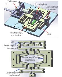
ObjectiveGlass-ceramic is a kind of optical hard and brittle material with broad application prospects in aerospace, medical treatment, electronics and other fields. Glass-ceramic is required to process the free-form surface on the surface in many application scenes. However, due to the high hardness and brittleness of the glass-ceramic itself, the processing difficulty is greatly improved. Therefore, it is necessary to develop a precision or ultra-precision processing method that can effectively improve the processing quality and efficiency of the free-form surface of glass-ceramic.MethodsIn this paper, laser assisted machining (LAM) and fast tool servo (FTS) technologies are combined to design a laser-assisted fast tool servo cutting device which can be used to cut the free-form surface shape of glass-ceramic, and the structure and working mode of the device are described. The elastic beam method is used to calculate the displacement amplification ratio of the diamond amplification mechanism in the flexure hinge mechanism. The deviation and displacement amplification ratio of the output displacement of the two levers displacement amplification mechanism in the flexure hinge mechanism are obtained through the static simulation. The equivalent stress of the flexure hinge mechanism is analyzed. The static laser irradiation temperature measurement experiment of glass-ceramic is carried out to obtain the maximum laser power threshold that can be withstood by the actually processed glass-ceramic. The laser assisted fast tool servo cutting experiment is carried out to obtain the free-form surface topography of glass-ceramic. The surface roughness after conventional FTS cutting and laser assisted cutting is compared and analyzed, and the influence of process parameters on the surface roughness is also analyzed.Results and DiscussionsThe theoretical displacement amplification ratio of the diamond amplification mechanism calculated by the elastic beam method is 2.83. The absolute error of the output displacement of the two levers displacement amplification output end of the flexible hinge mechanism is 0.17 μm through the static simulation, and the two can output synchronous displacement. The displacement amplification ratio is 6.35. The equivalent stress analysis results show that the maximum stress of the flexible hinge mechanism is less than the allowable stress of the material. The theoretical calculation and static simulation verify that the flexible hinge mechanism has good displacement amplification and output characteristics, and the mechanism is safe and reliable. The static laser irradiation temperature measurement experiment of glass-ceramic has determined that the maximum acceptable laser power in actual processing is 75 W. The free-form surface topography is obtained in the laser-assisted fast cutting experiment of glass-ceramic. The surface roughness decreases with the increase of laser power and the decrease of spindle speed. The maximum surface roughness reduction was 58.2% when laser power was 75 W.ConclusionsThe research shows that the laser assisted fast tool servo cutting method can improve the surface processing quality greatly compared with the conventional FTS cutting method when successfully cutting the free surface morphology of glass-ceramic.
Mar. 25, 2025Vol. 54 Issue 3 20240613 (2025)
Ruyi FENG, Yue ZOU, Jingyu HAO, Sijia WANG, Bowen LIU, Jintao FAN, and Minglie HU
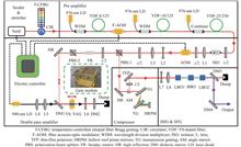
ObjectiveUltrafast laser with high power and high energy is widely used in industry and scientific research. The femtosecond laser power output of the mode-locked oscillator stage is usually low, and it is difficult to meet the application requirements, power amplification is performed in the subsequent amplifier stage. Compared with fiber amplifiers, solid state amplifiers have low nonlinear effects and high damage thresholds, so they can support higher energy femtosecond laser output. However, at the same time of obtaining high energy laser output, due to the thermal effect introduced by high power pumping, the beam quality is significantly reduced, and in some applications, the pulse energy is not required to be extremely high, only the mJ magnitude can be reached, and ask it has the characteristics of high beam quality, high pulse quality and high stability. Therefore, it is significant to study a compact single-stage solid-state amplifier, which can output mJ energy while maintaining a high level of beam quality.MethodsBased on femtosecond mode-locked laser and all-fiber pre-amplifier stage, combined with chirped pulse amplification technology, a two-pass wave amplification system based on Yb:YAG is constructed. In order to reduce the influence of thermal effect on beam quality and improve pump efficiency, periodic signal modulation is applied to pump control current to realize synchronous pulse pumping with adjustable duty cycle. In order to control the size of the spot in the process of amplification, the self-reproducing optical path is designed and simulated according to the simulation results of thermal lens, and the numerical reference is provided for the selection of focal length parameters of the compensated lens (Fig.2). In order to obtain femtosecond laser output with high pulse quality, the pulse output near the transformation limit is obtained by optimizing the angle and distance of the grating and adjusting the second and third order dispersion values of CFBG. Based on the compressed femtosecond fundamental frequency light with high energy, high beam quality and high pulse quality, a third harmonic converter based on compensation plate is built. By optimizing the parameters of the fundamental frequency light beam size and crystal thickness, the third harmonic generation can be achieved with high conversion efficiency.Results and DiscussionsThe results of solid-state laser amplification with different repetition rates, different pumping modes and different pulse pumping widths are studied. When the signal laser repetition rate is low, the optimal pump width is narrower, and the corresponding optimal duty cycle at 1 kHz is 47% (Fig.3(a), Fig.3(b)). Compared with continuous pumping, pulsed pumping has a higher utilization of pump power and can effectively disperse the thermal effect of high pump power at the time scale, with a higher gain potential while maintaining a high beam quality pulse output (Fig.3(c)). A severe gain narrowing effect occurred during solid amplification, with the spectrum narrowing by a factor of 4 before and after solid amplification (Fig.3(d)). A femtosecond laser output with an energy of 1.65 mJ and pulse width of 623 fs was obtained by compressing the amplified laser at full power, with a compression efficiency of up to 93% (Fig.4(a)). The derived depolarization power in the dual-pass system is measured, and its power ratio is stable below 3%, which proves that pulse pumping can effectively alleviate the thermal depolarization effect and obtain better beam quality (Fig.4(b), Fig.4(c)). Due to the use of pulse pumping, its amplification gain is not supersaturated and therefore has a high pulse energy stability (Fig.4(d)). The conversion efficiency of second and third harmonics at different crystal thicknesses is measured. When the crystal length is too long, the nonlinear action is too strong, resulting in susaturation of the rotation efficiency. When the thickness of the double frequency crystal and the sum frequency crystal are both 2 mm, the highest third-harmonic conversion efficiency is 26.5% (Fig.5(a), Fig.5(b)). Due to the limitation of phase matching bandwidth, the spectrum from infrared to green to ultraviolet laser gradually narrows (Fig.5(c)). The beam quality of the third harmonic is reduced due to the effect of higher order nonlinear effect and two-photon absorption effect (Fig.5(d)). The 2-hour power stability of infrared, green, and ultraviolet beams are all measured, and the results show that the system has a high long-term stability (Fig.5(e)).ConclusionsA high energy solid femtosecond laser system was built, and the influence of pulse pumping on the output performance of solid amplification was studied. When the signal repetition rate was low, under the action of short pump pulse width, not only the pump power utilization could be improved, but also the influence of thermal effect was greatly reduced, and the gain potential was higher while maintaining high beam quality pulse output. The high energy and high beam quality femtosecond laser pulse output is obtained with repetition frequency of 1 kHz, energy of 1.65 mJ, pulse width of 623.4 fs, beam quality factor of 1.14, peak-to-peak power stability of 5.0% and energy stability of 1.11%(RMS). Moreover, the characteristics of high energy, high beam quality and high pulse quality lay a good foundation for efficient generation of third harmonic. The UV light with single pulse energy of 0.438 mJ and center wavelength of 344.35 nm was obtained, and the overall conversion efficiency was 26.5%. The third harmonic conversion efficiency reached the advanced level.
Mar. 25, 2025Vol. 54 Issue 3 20240614 (2025)
Lei YANG, Haoran XIONG, Hanming WU, Shendong LIU, Yongtian WANG, and Lingling HUANG
Significance Reconfigurable metasurfaces composed of subwavelength structural units can dynamically adjust the propagation characteristics of light waves, such as phase, amplitude and polarization. They exhibit significant application potential across various fields. In order to realize the reconfigurability of metasurfaces, materials with special properties are usually utilized to make them react dynamically under specific external stimuli, such as electric field, magnetic field, heat, light, etc. Compared to traditional optical components, reconfigurable metasurfaces offer greater flexibility and customizability, making them highly advantageous in high-resolution imaging, dynamic displays, intelligent sensing, optical computing, and wireless communication. With the rapid development of information technology, optical technology, and nanofabrication techniques, reconfigurable metasurfaces can provide new design ideas for next-generation intelligent optical devices.Progress First, this article introduces the basic principles and control mechanisms of reconfigurable metasurfaces, including electrical control, thermal control, phase-change material-based control, optical field control, chemical control, mechanical control and so on. Reconfigurable metasurfaces based on different manipulation mechanisms have unique advantages, but they inevitably come with certain limitations. The control mechanism based on the electro-optic effect has the advantages of fast response and high control precision, but it often requires complex circuit design. Magnetic field control, which relies on the magneto-optic effect or spin effect, adjusts the material's refractive index or optical rotation characteristics via an external magnetic field. This method is typically used in magneto-optical devices and offers the advantage of no physical contact; however, its response speed is slower, and it requires a high-intensity magnetic field, which limits its potential for miniaturization. The thermo-optic effect can achieve optical modulation over a wide wavelength range, but its response speed is relatively slow and cannot meet the demands of high-speed dynamic applications. Phase-change material-based metasurfaces excel in achieving multi-state dynamic control, but the complexity of material processing and long-term stability still need further optimization. Mechanical control is suitable for large amplitude and multi-degree-of-freedom changes in optical characteristics, but there are challenges in terms of micro-nanoscale integration and repeatability.In addition, the article provides a detailed overview of the research progress of reconfigurable metasurfaces in dynamic imaging and display, optical computing, and wireless communication. By precisely controlling light waves, reconfigurable metasurfaces can adjust parameters such as focal length and wavefront during dynamic imaging, showing broad application prospects in dynamic imaging systems that require real-time optical performance adjustments. As a new type of optical element with reprogrammable characteristics, reconfigurable metasurfaces can be used in optical computing to perform mathematical calculations or logical operations, such as Fourier transforms, differentiation, and integration, enabling the processing of optical signals. They can also be further applied in neural networks to independently perform complex tasks such as image recognition and deep prediction. In wireless communication systems, reconfigurable metasurfaces enhance signal modulation and transmission capabilities through their dynamically adjustable properties, such as dynamically controlling the phase, amplitude, and polarization states of metasurface units, enabling dynamic beam shaping, multiplexing, and demultiplexing.Conclusions and Prospects Finally, the article summarizes the challenges that reconfigurable metasurfaces face in practical applications, such as response speed, precision, multifunctional integration, stability, and large-scale manufacturing. It further envisions the future research directions of reconfigurable metasurfaces, which will focus on improving the response speed and precision of materials, optimizing structural design to achieve more diversified functional integration, and exploring low-cost, high-stability manufacturing processes. Additionally, the integration of artificial intelligence and advanced computational methods will further drive the intelligent design and dynamic control capabilities of metasurfaces, enabling more complex and precise optical operations. With continuous advancements in materials science, manufacturing processes, and computational technologies, reconfigurable metasurfaces will play an increasingly important role in fields such as optical communication, intelligent sensing, and dynamic display.
Mar. 25, 2025Vol. 54 Issue 3 20240620 (2025)
Yang ZHANG, Yipin SU, Yongkang LU, Junqing LI, Qihang CHEN, Ruidi YAN, and Wei LIU
ObjectiveThermal offset in Enhanced Reference System (ERS) points under non-uniform temperature fields is one of the primary factors causing reduced coordinate registration accuracy between the tooling measurement coordinate system (MCS) and the global coordinate system (GCS). Addressing this issue is critical for ensuring precision in large-scale metrology and aircraft assembly. This study aims to address the challenges posed by sparse measurement points, complex temperature distributions, and finite element model simplifications, which collectively limit the accuracy of temperature field modeling and thermal offset prediction. A novel method integrating global temperature field reconstruction, virtual measurement point dynamic optimization, and coordinate registration error compensation was developed to improve the accuracy and reliability of thermal offset prediction and registration.MethodsA novel methodology integrating virtual measurement point dynamic optimization and precise temperature field reconstruction was proposed to address the challenges of thermal offset prediction and coordinate registration under non-uniform temperature fields. First, a global temperature field reconstruction algorithm (GPR-GTFR) based on Gaussian Process Regression was developed to accurately capture the spatial distribution characteristics of complex non-uniform temperature fields, providing high-quality input data for subsequent thermal offset prediction. Next, a thermal offset prediction model was established using the finite element method (FEM) to quantitatively analyze the thermal displacement of ERS points under varying temperature conditions. To overcome the limitations of sparse measurement point distributions and inaccuracies caused by FEM model simplifications, a virtual measurement point dynamic optimization strategy was proposed. This strategy incorporated an improved Adaptive Dynamic Local Search Prairie Dog Optimization algorithm (ADLSPDO) to dynamically optimize the spatial layout of the temperature field, enhancing the spatial coverage and accuracy of temperature field reconstruction. Finally, the predicted thermal offset values were used to correct the nominal positions of ERS points, effectively reducing the coordinate registration errors between the tooling measurement coordinate system (MCS) and the global coordinate system (GCS). The proposed methodology was validated through simulations and experiments to verify its effectiveness in addressing thermal offset challenges.Results and DiscussionsThe proposed method was evaluated through a series of experiments and simulations, and its effectiveness was verified at multiple levels. The GPR-GTFR algorithm demonstrated superior accuracy and robustness compared to traditional Kriging methods in reconstructing temperature fields, particularly under sparse measurement conditions (Fig.6). The introduction of dynamically optimized virtual measurement points significantly improved the spatial coverage and accuracy of temperature field modeling, reducing errors in thermal offset predictions (Tab.2). Furthermore, the coordinate registration compensation results showed that the Root Mean Square Errors (RMSE) in the X, Y, and Z directions after compensation were reduced by 84.5%, 77.9%, and 78.8%, respectively (Tab.3, Fig.14). These findings highlight the proposed method’s ability to mitigate thermal offset effects and enhance the accuracy of coordinate registration between the tooling MCS and the GCS.ConclusionsThis study presents an integrated methodology combining precise temperature field reconstruction, dynamic optimization of virtual measurement points, and coordinate registration compensation to address thermal offset challenges in tooling ERS points under non-uniform temperature fields. Compared to existing methods, the proposed approach demonstrates significant improvements in thermal offset prediction accuracy and registration precision, particularly under sparse measurement conditions and modeling simplifications. The results validate the robustness and reliability of the method for maintaining ERS point precision in challenging thermal environments. However, further research is required to improve computational efficiency and adapt the methodology to real-time applications and more complex industrial scenarios. The findings of this study provide valuable insights and practical solutions for enhancing precision in large-scale metrology and aircraft assembly.
Mar. 25, 2025Vol. 54 Issue 3 20240623 (2025)
Yingxiao MA, and Ziyuan LI
Significance Multispectral imaging technology has made significant progress in photodetection due to its high-dimensional information. This progress is driven by two factors: innovations in multispectral technology combined with the development of interdisciplinary fields such as materials science, nanotechnology, and artificial intelligence, which have transformed multispectral technology from traditional to novel detection techniques. The spectral splitting methods of novel detectors have transitioned from macro-scale to micro-scale, leading to enhanced performance that surpasses traditional systems. The demand for miniaturized, lightweight detectors has further accelerated the development of on-chip multispectral photodetectors. Recent innovations in high-integration and high-sensitivity methods and materials have laid a solid foundation for future on-chip multispectral technologies. It is clear that multispectral photodetectors will evolve from large-scale systems to on-chip designs, highlighting the significance of this survey on multispectral photodetectors.Progress First, the spectral splitting methods of multispectral photodetectors are introduced, which can be categorized into three types: dispersion-based, filter-based, and interference-based methods. These methods typically rely on large discrete optical components, such as gratings, triangular prisms, large-aperture lenses, and multiple sets of filters. However, these components often suffer from poor stability and are difficult to integrate, which increases the overall volume and complexity of the system. As a result, such designs deviate from the current trend toward miniaturization in multispectral photodetection. In contrast, the new generation of on-chip multispectral detectors offers greater flexibility in light splitting. These detectors either utilize ultra-thin or pixel-based splitting surface arrays that can be directly integrated with the detector or employ innovative optoelectronic materials that simultaneously function as both photosensitive and spectroscopic components. This approach enables the integrated design and manufacturing of multispectral detectors, significantly advancing the field.After introducing the principles of multispectral detection, the development progress of novel on-chip multispectral detectors is detailed. Semiconductor nanowires-based and active nanoantenna-based multispectral detectors can achieve wavelength-selective and efficient detection from the visible light to the infrared region by simply adjusting the diameter of the nanowires/nanopillars, making them ideal candidates for photodetection across a wide spectral range from ultraviolet to infrared. Quantum dot-based multispectral detectors effectively compensate for the deficiencies in the infrared wavelength range of multispectral detection. By reasonably designing the photoresponse range, they can almost cover the entire infrared range from near infrared to long-wave infrared. However, the uniformity and stability of quantum dots are challenges that need to be urgently overcome. Two-dimensional material-based multispectral detectors take advantage of the atomic thin-layer characteristics of two-dimensional materials, which can achieve a high detectivity, but the impact of filter usage on system complexity cannot be completely eliminated. Perovskite-based multispectral detectors benefit from the flexibility and designability brought by the octahedral symmetry structure of perovskites. Their photoresponse range can be flexibly tuned from the ultraviolet to the near-infrared range. However, their lack of stability and the presence of toxic lead currently hinder the commercialization and large-scale application of perovskite materials.The primary application fields for multispectral detectors include remote sensing satellites, drones, and airborne platforms, and the application scenarios are highly diverse. They could be utilized not only in natural environments, such as estimating cloud top height, detecting thick cloud positions, inverting aerosol optical thickness, identifying land features, measuring rice nitrogen content, detecting floods, inverting ocean depth, and identifying marine plastic waste, but also in human-related fields. These include assisting in skin cancer screening and treatment, monitoring diabetic retinopathy, assessing human stress levels, aiding in the diagnosis of psychological conditions such as depression and anxiety, detecting fire points, inspecting food quality, protecting natural heritage, and supporting archaeological research.At the conclusion of this paper, the main challenges multispectral photodetectors are facing are summarized, and several recommendations are proposed. These insights aim to provide valuable guidelines for the development and research of multispectral photodetectors in China.Conclusions and Prospects The field of multispectral imaging photodetectors is transitioning from traditional to emerging technologies. Traditional detectors provide excellent stability and reliability, establishing a strong foundation for commercialization. However, their complexity and sensitivity limitations constrain performance enhancement and application expansion. In contrast, new detectors, which incorporate innovative methods and materials, are driving revolutionary advancements. Currently, both material selection and device fabrication are in the early stages of exploration and optimization, requiring more efforts to accelerate the development of these technologies. Despite ongoing technological and cost challenges, multispectral detectors show significant potential. As global demand for multispectral imaging continues to rise, the development of high-precision, compact, fast-response, and high-resolution detectors has become a key area of research.
Mar. 25, 2025Vol. 54 Issue 3 20250042 (2025)
Qing WANG, Xiaoyu YANG, Pengwei LI, and Shu CHEN
Significance Terahertz (THz) waves, situated between microwaves and infrared radiation, own strong penetration capabilities, low photon energy, and high biological safety, demonstrating significant application potential in fields such as material detection, biomedicine, communications, and astronomy. However, the advancement of THz technology still encounters numerous challenges, particularly in the development of efficient radiation sources, detectors, and ultra-sensitive detection and modulation devices. Polaritons, which are quasi-particles formed by the coupling of light with electrons and phonons in matter, can enhance the interaction between light and matter in the THz frequency range, offering promising solutions to the bottlenecks in THz optoelectronic devices. Low-dimensional materials, such as graphene, Bi2Se3, and Ag2Te, with their nanoscale thickness, tunable carrier concentration, and rich lattice structures, exhibit polaritons with low loss, high optical field confinement, enhanced optical fields, and high tunability. These characteristics provide additional opportunities to address the challenges in the field of THz science and technology.Progress Since its discovery in 2004, graphene has been shown to support plasmon polaritons from massless Dirac carriers. Using methods like gate electrodes and chemical doping, these polaritons can operate in the IR to THz range. In 2011, researchers first measured plasmonic resonances in far-IR to THz frequencies in graphene ribbons, confirming their high field confinement and tunability. Later, in 2016, THz near-field microscopy with photocurrent detection enabled real-space imaging of graphene acoustic plasmon polaritons (APPs), revealing their superior field localization and compression over optical modes. Leveraging APPs enables further exploration of non-local quantum effects (Fig.5). Dirac carriers are not exclusive to graphene but are also widely present in low-dimensional topological insulator materials, such as Bi2Se3. THz plasmon polaritons in Bi2Se3 were first reported in 2013 and was claimed from the Dirac carriers. In fact, the plasmon polaritons in Bi2Se3 may be also contributed by bulk carriers and optical phonons, in addition to Dirac carriers. In 2022, researchers achieved real-space imaging of THz polaritons in Bi2Se3 and revealed that the polaritons arise from the combined contributions of bulk-doped carriers, Dirac carriers, optical phonons, and a two-dimensional electron gas induced by surface state band bending (Fig. 6). In contrast to the in-plane isotropic plasmon polaritons described above, recent studies have shown that WTe2 can support far-IR in-plane hyperbolic plasmon polaritons (Fig.7), which exhibit extremely large plasmon wavevectors, resulting in exceptionally high optical field localization and optical density of states (Fig.7). More recently, researchers using terahertz scattering-type scanning near-field optical microscopy discovered that Ag2Te can support in-plane anisotropic plasmon polaritons. They quantitatively measured the plasmon dispersion using APPs, demonstrating that APPs can not only enhance the localization and compression of THz fields but also improve the propagation quality of the polaritons. Compared to plasmon polaritons, phonon polaritons exhibit significantly lower losses. To date, materials such as α-MoO3 and α-GeS have been identified as supporting THz phonon polaritons. Specifically, α-MoO3 has been found to sustain in-plane hyperbolic phonon polaritons within the frequency range of 7.8 to 11.7 THz (Fig. 8), with an impressive polariton lifetime of up to 9 ps. Similarly, α-GeS supports anisotropic phonon polaritons in the THz range (6.1 to 9.5 THz), characterized by long lifetimes and high Q-factors. Significant progress has been made in modulating low-dimensional material polaritons using strategies like twist-angle engineering, doping, and polarization control. For example, in α-MoO3, adjusting the interlayer twist angle triggers a topological shift from hyperbolic to elliptic polaritons, creating non-diffracting, directional channel modes (Fig.9). In WTe2, molybdenum doping changes phonon polariton dispersion from elliptic to hyperbolic (Fig.9), while controlling the polarization angle of incident light induces a similar transition in plasmon polaritons due to polarization-dependent surface resonance (Fig.9).Conclusions and Prospects This article reviews recent progress in THz polariton photonics in low-dimensional materials, highlighting their exceptional properties like high field confinement, near-field enhancement, strong light absorption, and tunability, which hold great promise for THz optoelectronic devices. While significant advances have been made, many questions remain, and new research opportunities are emerging. Future work will focus on exploring diverse THz polariton systems, such as Cooper pair and magnon polaritons, to uncover new phenomena and applications. It will also develop advanced modulation techniques for precise control and design polariton-based devices like ultra-sensitive sensors and room-temperature photodetectors, addressing current THz technology challenges.
Mar. 25, 2025Vol. 54 Issue 3 20250058 (2025)
Jinshuai DU, Yin DENG, Shiyang CAO, Zeying LU, Jie LI, Zhuo HAN, Jinmin ZHOU, Ke WANG, Lili GUI, and Kun XU
Significance Although current artificial intelligence (AI) systems, especially deep learning models, have made significant progress in multiple fields, they still face problems such as high energy consumption, low interpretability, and insufficient flexibility. In contrast, in vitro Biological Neural Networks (BNN) are based on real biological neurons. Through their unique dynamic plasticity and adaptive learning capabilities, they can complete complex information processing tasks with low power consumption, laying the foundation for AI. Energy efficiency, interpretability and flexibility lead to completely new solutions. In addition, in vitro BNN uses precise culture technology and advanced control methods to enable the function and structure of neural networks to be precisely controlled, thereby providing an experimental platform for understanding the working mechanism of the brain, optimizing intelligent computing systems, and advancing brain-computer interface technology. Although the current computing performance of BNN is still in its infancy, its characteristics provide important directions and ideas for the development of efficient intelligent computing systems in the future.Progress In recent years, bio-intelligent computing based on in vitro BNN has made significant progress in culture technology, signal monitoring and application scenarios. Through breakthroughs in two-dimensional and three-dimensional culture technology, BNN can more realistically simulate the biological brain neural network structure and promote the optimization of neural network functions. At the same time, combining multiple input methods such as electrical, optical and chemical stimulation allows neuronal activity to be precisely controlled, providing a new experimental platform for task adaptation and complex information processing. In terms of applications, BNN has shown great potential in static tasks (such as speech recognition) and real-time interactive tasks (such as neurorobot control), especially in dynamic learning, complex pattern recognition, and real-time tasks. In addition, the low power consumption characteristics and adaptive capabilities of BNN provide new ideas for the development of intelligent computing systems. In the future, with the further integration of neuroscience and computing technology, biological intelligent computing based on BNN is expected to usher in revolutionary progress in the fields of brain-computer interfaces, intelligent computing systems, and brain-like computing.Conclusions and Prospects Research on biological intelligent computing based on in vitro BNN has shown great potential to break through the bottleneck of traditional artificial intelligence and has obvious advantages in dynamic adaptation and complex pattern recognition. However, despite the initial results, BNN still face challenges in terms of computational efficiency, scalability, and compatibility with traditional computing systems. Future research will focus on further improving system integration, solving technical bottlenecks, and promoting the combination of BNN with existing computing technologies. With the advancement of technology and the deepening of interdisciplinary research, it is expected to promote the widespread application and in-depth development of biological intelligent computing in AI.
Mar. 25, 2025Vol. 54 Issue 3 20250073 (2025)
Tianlun LI, Yancheng SU, Tongze XIA, Leping YANG, Shuaiwei JIA, Zhuang XIE, and Duorui GAO
Significance Optical parametric amplification (OPA) is recognized as a crucial technique for mitigating signal attenuation in both fiber and free-space optical communication systems. Conventional optical amplifiers are mostly phase-insensitive, such as erbium-doped fiber amplifiers (EDFAs), which are extensively employed in fiber-optic communications system. However, the signal-to-noise ratio (SNR) and link distance of the communication system are difficult to break the bottleneck due to a 3 dB noise figure limit brought by the phase-insensitive amplification. In contrast, phase-sensitive amplification (PSA) utilizing nonlinear optical frequency-mixing shows promise for near 0 dB noise figure as well as high amplification gain. PSA is one of the most potential technologies for optimizing communication performance, extending link distance, and all-optical signal processing. Herein, we will introduce the PSA technology and look forward to its application prospects in the research field of optical communication.Progress PSA technology mainly relies on four-wave mixing (FWM) or three-wave mixing (TWM). Nonlinear optical medium that possesses large third-order nonlinear susceptibility coefficients is considered as ideal choice for achieving FWM-PSA, such as highly nonlinear fiber (HNLF) and silicon nitride (Si3N4) waveguide. Typically, FWM-PSA contains two separate HNLFs for cascaded FWM. The first-stage FWM generates a phase-matched idler signal and enables energy transfer from the pump to the signal and idler when specific phase conditions are satisfied. Although the signal is amplified via the energy flow, it is phase-insensitive amplification (PIA). Then, the second-stage FWM is the critical step for PSA. The idler produced in PIA along with the pump and signal is injected in second HNLF, the PSA is achieved while the three components mutually phase-matched. The phase-match condition is satisfied to guarantee the direction of energy flow. The achievement of TWM-PSA relied on the optical medium which can provide larger second-order nonlinear optical susceptibility, such as periodically poled lithium niobate (PPLN). This process primarily employs second harmonic generation (SHG) and difference frequency generation (DFG) to amplify signal. The SHG produced a phase-matched idler which has the same frequency as the pump in cascaded DFG. Thus, the efficiency of DFG can be increased to achieve higher amplification gain. Precise control of the phase relationship between the pump, signal and corresponding idler is required to optimize gain and noise figure. Additionally, the innovation of optical material and structure can also bring beneficial effects for enhancing the performance of PSA, such as Aluminum Gallium Arsenide (AlGaAs) waveguides and graphene-based hybrid structures. By enhancing the nonlinear coefficients, these materials or structures lead to higher amplification gain and lower loss.Conclusions and Prospects OPA is widely considered a significant advancement in optical communication systems. PIA-type amplifier, such as EDFA, has been in development for a much longer time and has entered engineering applications. Although PSA technology is not as mature as EDFA, it is able to overcome the 3 dB quantum noise limit and has better amplification gain and noise figure. The next step for the PSA research focuses on the integrated devices, which are bringing new blood into the fabrication of laser communication terminal with SWaP (Size Weight and Power) limitation. At the same time, PSA still faces technical challenges for practical application, including the integration of PSA and photodevice, weak optical detection by chip-level devices, and the phase-matching adaptation assisted by artificial intelligence in variable communication environments. However, PSA technology plays a crucial role in ultra-long-distance communication link, massive data optical interconnections, and optical-wireless convergence. It is expected to promote the development of core components for next-generation optical communication systems. PSA has broad application prospects for increasing communication speed and enhancing its link quality by overcoming limitations in noise, bandwidth, and signal-reliability.
Mar. 25, 2025Vol. 54 Issue 3 20250103 (2025)
Ziyang ZHANG, Yunshuai MI, Lin JI, Yun XIAO, Wei XIA, Yulong LIU, and Yunhai ZHANG
ObjectiveCommon human fundus diseases, such as Age-Related Macular Degeneration (AMD), Diabetes Retinopathy (DR), Retinitis Pigmentosa (RP), etc., affect 60 million people worldwide. They are the main blindness cause of human. The autofluorescence of the fundus is closely related to the metabolism of the fundus. The autofluorescence imaging of the fundus can obtain more detailed and special fundus information, judge in advance the position where fundus diseases may occur, and accurately locate the position where fundus diseases have occurred. Due to the fact that eye fundus diseases often develop from surrounding areas, they are often missed in the early stages of the disease due to insufficient imaging field angles. Therefore, it is hoped that the imaging field angle can reach 90° at the pupil for a larger range of examination of the fundus. It is necessary to establish animal models for diagnosis and study human fundus diseases. As the structure and composition of rat eyes and human eyes are basically the same, rats are often used as animal models for human fundus disease research. Rat models can be used to replace human eyes for numerous studies related to human fundus diseases. At present, there is no method that can be directly used for ultrawide-angle fundus autofluorescence imaging in rats. Therefore, the development of methods and techniques for ultrawide-angle fundus autofluorescence imaging in rats is of positive significance for expanding the research methods of fundus diseases and developing related fundus disease inspection instruments. For this purpose, an ultrawide-angle fundus autofluorescence imaging system for rats was studied, which can perform fundus autofluorescence imaging on rats. Using rats to carry out related research on human fundus diseases can reveal the pathogenesis and process of human fundus diseases, and provide reference for the development of ultrawide-angle fundus equipment.MethodsThe ultrawide-angle fundus autofluorescence imaging system for rats in this article is based on laser scanning confocal imaging technology. By using self-developed lens and two-dimensional scanning galvanometer, the scanning angle at the pupil reaches 90° (equivalent to a field of eye-angle of 132.3°), meeting the field of view requirements of ultrawide-angle fundus imaging. The fundus autofluorescence signal is obtained by using a filter with optimized light transmission range. Finally, the original images of rat fundus autofluorescence were registered and superimposed using SURF algorithm to obtain high-quality rat fundus autofluorescence images.Results and DiscussionsBuilding an ultrawide-angle fundus autofluorescence imaging system in rats. The simulation shows that the illumination system not only has excellent image quality, its RMS radius is close to the Airy spot radius (Fig.3(b)), the MTF curve is close to the diffraction limit (Fig.3(c)), but also the aberration is small and the maximum distortion is only 8.7% (Fig.3(d)). The average horizontal field of view obtained from the three measurements was 90.38°, and the vertical field of view was 91.50° (Tab.2), which met the design requirements of the designed scanning field of view and could be called ultrawide-angle fundus imaging. At 488nm wavelength, the system resolution was 16.4 μm (Fig.8(b)), which was slightly larger than the theoretical resolution of 13.2 μm obtained from the RMS spot diagram radius. Considering the factors such as aberration, noise and measurement error, the test results of the system are in accordance with the actual situation. Sprague Dawley (SD) rats were used for imaging experiments to obtain fundus autofluorescence images of SD rats. The signal-to-noise ratio of three superimposed fundus autofluorescence images of SD rat was 8.64 (Fig.10(d)). The image quality can meet the requirements of ultrawide-angle fundus autofluorescence imaging. This system can be used for ultrawide-angle fundus autofluorescence imaging in rats.ConclusionsAn ultrawide-angle fundus autofluorescence imaging system for rat was designed. The principle of the system is clear and the structure is simple. The self-developed lens is used to achieve ultrawide-angle fundus imaging with a pupil scanning angle of 90°, which is equivalent to 132.3° of the eye-angle. The system resolution is 16.4 μm at a wavelength of 488 nm. A confocal pinhole filter was used to filter out stray light in the focal plane, and the combination of fluorescence signal bands was set to obtain fundus autofluorescence signals. Finally, the three original ultrawide-angle fundus autofluorescence images of rats were superimposed, and the signal-to-noise ratio was increased to 8.64, which met the requirements of ultrawide-angle fundus autofluorescence images, promoted the research of fundus diseases, and provided a reference for the development of ultrawide-angle fundus imaging equipment.
Mar. 25, 2025Vol. 54 Issue 3 20240399 (2025)
Yang’aoxiao FU, Mingsong DING, Qingzong LIU, Peng LI, Weizhong DONG, Tiesuo GAO, and Tao JIANG
ObjectiveWhen high-speed tandem layout vehicle reaches predetermined separation point, payloads needs to separate from the booster, in order to separate successfully, it is feasible to apply jet thruster on the booster to provide reverse thrust, thus makes the booster separate safely from the payloads. During this stage separation, high-temperature gas ejected from jet thruster not only generates strong infrared radiation, but also affect the temperature distribution on vehicle’s surface, which ultimately affects the radiation characteristics of the target. Meanwhile, due to the high flight speed, inflow air and jet gas in flow field will be involved in complex chemical reactions such as dissociation, ionization and afterburning, which can also significantly affect the radiation characteristics of the target. In the field of aircraft detecting and tracking, most researches focuses on aircraft’s steady state infrared radiation characteristics, while the transient radiation characteristic during the stage separation is a typical characteristic different from those steady state characteristics, investigation on this transient radiation characteristic can provide useful reference for aircraft detecting and tracking application. This paper investigates the influence of high-speed aircraft’s stage separation on target infrared radiation characteristics, the infrared radiation characteristics of flow field and aircraft’s surface is analyzed, the influence of jet gas’s chemical reaction, observation wave bands and observation angles on radiation characteristics is also studied.MethodsTypical lifting body payload with booster is used as research object (Fig.3), three-dimensional Navier-Stokes equation with chemical reaction source term is solved to simulate the high-speed aircraft’s stage separation flow field, the chemical reactions of jet gas and inflow air is considered. By using radiative equilibrium wall condition, vehicle’s surface temperature is calculated. The radiative transfer equations are solved based on statistical narrow band model and apparent light method. A Cartesian coordinate system is used to describe the radiation distribution, the observed angles are represented by zenith angle θ and circumferential angle φ (Fig.8).Results and DiscussionsDuring the stage separation, infrared radiation sources include the infrared radiation from the vehicle’s high temperature wall, and the infrared radiation from the high temperature gas components in flow field, however, the infrared radiation intensity of them is roughly in the same order of magnitude (Fig.9). Infrared radiation of flow field is mainly contributed by CO2 and H2O, the contribution of other components is relatively small, spectral radiation curve has two obvious peaks of 2.7 μm and 4.3 μm (Fig.10). When jet thruster on booster stage works, compared with jet off condition, the target infrared radiation intensity of aircraft increases significantly, the radiation intensity can be increased several times at specific wave band and detection angle (Fig.11). The infrared radiation intensity of upside observation is slightly higher than that of downside observation (Fig.11), which is due to the existence of flight angle of attack and the wall temperature in windward region is higher than that of leeward region (Fig.7). The radiation intensity of 1~3 μm band is the largest, which can reach 2~3 times of other bands under specific detection angle (Fig.11), this is because the peak value of infrared radiation generated by wall is near the wavelength of 1 μm (Fig.9), while the radiation generated by the flow field is mainly contributed by H2O and CO2, whose infrared radiation peak are also near the wavelength of 1~3 μm (Fig.10). When considering the chemical reactions of jet gas, the target infrared radiation intensity of aircraft can drop up to 50% at specific wave band and detection angle (Fig.11), this is because the high flight altitude and low inflow oxygen density, afterburning reaction is weak, and due to the high flight speed and high temperature in the shock layer, jet gas components mainly involves in dissociation reaction, which makes flow field temperature and the mass fraction of H2O and CO2 drops (Fig.12, Fig.13), thus makes the target infrared radiation intensity drops significantly.ConclusionsDuring the high-speed aircraft’s stage separation, infrared radiation intensity of flow field and aircraft’s surface are almost in the same order of magnitude, infrared radiation in flow field is mainly contributed by CO2 and H2O; The radiance enhancement caused by jet gas is significant, target radiation intensity can increase up to several times, the radiation intensity at 1~3 μm band is the strongest; Due to high flight speed, jet gas components mainly involve in dissociation reaction, which makes flow field infrared radiation intensity drop up to 50%, and this is different from the situation in low altitude where the jet gas’s afterburning effect can make flow field infrared radiation intensity increase significantly.
Mar. 25, 2025Vol. 54 Issue 3 20240398 (2025)
Zhengxin SONG, Wenjie ZHANG, Chong ZHENG, Shangyu ZHANG, and Linhua LIU
ObjectiveAccording to the Stefan-Boltzmann’s law, infrared (IR) stealth can be realized by reducing both the surface temperature and the surface IR emissivity. In the practical applications of IR stealth coatings, in order to reduce the surface temperature of high-power military equipment, a thermal protection layer is often stacked between the particle-composite low emissivity coating and the bare equipment skin surface. However, the radiation transfer process in the stacked structure will differ from the case of only particle-composite low emissivity coating used, hence the apparent emissivity of the stacked IR stealth coatings will deviate from the originally designed particle-composite low emissivity coatings, which will further affect the IR stealth performance. Therefore, it is of great engineering importance to investigate the effects of the material and thickness of the thermal protection layers on the apparent emissivity of the stacked particle-composite IR stealth coatings.MethodsA structure model composed of particle-composite low emissivity coating, thermal protection layer and substrate is built (Fig.1). The filler particles are simplified to be spherical and distributed uniformly in the top particle-composite low emissivity coating layer. The Finite-Difference Time-Domain (FDTD) method is applied to simulate the electromagnetic response of the stacked structure in the spectral range of 3-14 μm. The spectral average emissivity of the stacked structure is extracted to investigate the effects of the thickness of the thermal protection layer of different material (YSZ, SiO2 aerogel, and other materials of different complex refractive index). Moreover, the power absorption density distribution is calculated to analyze the mechanism of the thermal protection layer on the apparent emissivity.Results and Discussions The apparent spectral emissivity of the IR stealth coating is increased after a YSZ or SiO2 aerogel thermal protection layer is added between the particle-composite layer and the bare skin surface (Fig.5). The spectral average emissivity within the long-wavelength IR detecting range of 8-14 μm increases from 0.27 to 0.61 and 0.49 when the thickness of YSZ and SiO2 aerogel thermal protection layer increases from 0 to 20 μm respectively (Fig.6), while the variation within the long-wavelength IR detecting range of 3-5 μm is relatively low, which indicates that the IR stealth coating has begun to lose its low emission characteristics. The sensitivity of the emissivity to the thermal protection layer thickness is rarely affected by the embedded-particle size and volume fraction in the top particle-composite layer (Fig.7, Fig.8), but mainly depends on the intrinsic radiative properties (the complex refractive index) of the thermal protection layer. The variation of the apparent emissivity with the thickness of the thermal protection layer of different complex refractive index shows that the sensitivity of the emissivity to the thermal protection layer thickness is mainly dominated by the imaginary part of the complex refractive index, namely the absorption coefficient of the thermal protection layer. The higher the absorption coefficient of the thermal protection layer, the more sensitive the apparent emissivity of the stacked IR stealth coating is to the thermal protection layer thickness (Fig.10). The underlying mechanism of the apparent emissivity variation with the thermal protection layer thickness can be proved by the Kirchhoff’s law and the power absorption density distribution in the thermal protection layer: 1) more strong absorption zones will be included as the thermal protection layer thickness increases, which will lead to more absorption of the incident energy (Fig.11); 2) more energy will be absorbed by the thermal protection layer with high absorption coefficient after the incident light is transmitted through the particle-composite layer (Fig.12).ConclusionsThe YSZ or SiO2 aerogel thermal protection layer stacked between the particle-composite low emissivity coating and the bare equipment skin surface will increase the apparent emissivity of the IR stealth coating, and the apparent emissivity increases with the increase of the thermal protection layer thickness. The intrinsic absorption coefficient of the thermal protection layer is the dominant factor for the sensitivity of the apparent emissivity of the stacked IR stealth coating to the thermal protection layer thickness. The higher absorption coefficient, the more sensitive the apparent emissivity is to the thermal protection layer thickness, which may cause the IR stealth coating lose its low emissivity characteristics. Therefore, in the design and applications of particle-composite IR stealth coating, the improvement of the stealth performance by stacking thermal protection layers should be comprehensively evaluated from both increasing thermal conductive resistance and suppressing the apparent IR emissivity, the material and thickness of the thermal protection layer should be selected carefully and reasonably.
Mar. 25, 2025Vol. 54 Issue 3 20240404 (2025)
Zelong WANG, Jie FAN, Haizhu WANG, Yonggang ZOU, Linlin SHI, and Chong ZHANG
ObjectiveNarrow linewidth, fundamental transverse mode semiconductor laser devices are ideal optical sources for laser communication applications. To achieve a narrow linewidth and fundamental transverse mode output from semiconductor lasers, this study introduces lateral coupled gratings and lateral loss structures on both sides of the ridge waveguide of a broad-area semiconductor laser. These modifications aim to narrow the linewidth and suppress higher-order transverse modes. The device features etched loss structure areas on both sides of the 50 μm wide ridge waveguide, with a length of 150 μm and a lateral etching depth of 10 μm. The length of the lateral coupled grating is 700 μm, with a period of 6.3 μm and a duty cycle of 0.4. Experimental results indicate that at an injection current of 0.6 A, the output beam of the laser device maintains a “single-lobe” state, with a divergence angle of 5.92° and a spectral linewidth of 46 pm and the wavelength is 1 058.7 nm. Compared to the wide ridge waveguide laser (WR-LD), these values represent reductions of 16.5% and 59.6%, respectively. The laser device achieves an output power of 259.19 mW and a slope efficiency of 0.52 W/A, which corresponds to increases of 25.6% and 33.3% compared to the WR-LD.MethodsBased on the finite-difference time-domain (FDTD) method, this study utilizes higher-order lateral coupled gratings to narrow the linewidth and analyzes the relationship between limiting factors and etching depth. The lateral loss structure enhances the gain difference between the fundamental mode and higher-order transverse modes. By employing a loss clipping mechanism, it raises the gain threshold of the higher-order transverse modes, enabling fundamental transverse mode output at high current levels.Results and DiscussionsThe threshold current of the LM-LC-DFB with the added lateral loss structure is approximately 120 mA, while the threshold current of the WR-LD is 90 mA. At a drive current of 0.3 A, the LM-LC-DFB achieves an output power of 85.17 mW. As the drive current increases further to 0.6 A, the LM-LC-DFB obtains an output power of 259.19 mW and a slope efficiency of 0.52 W/A. Although the threshold current has increased, the output power and slope efficiency of the LM-LC-DFB are enhanced by 25.6% and 33.3%, respectively, compared to the WR-LD, which has output power and slope efficiency of 206.3 mW and 0.39 W/A, respectively. At a drive current of 0.5 A, the device with lateral coupled gratings has a center wavelength of 1058 nm, exhibiting stable single-peaked output with a 3 dB spectral linewidth of 46 pm. In contrast, the output spectrum of the WR-LD device displays two small peaks at the peak position, with its 3 dB spectral linewidth increasing to 114 pm, resulting in a linewidth narrowing of approximately 59.6%.ConclusionsWe have analyzed and developed a high-order laterally coupled grating DFB semiconductor laser with a loss structure. By simultaneously fabricating the loss structure and the laterally coupled grating structure on both sides of the wide ridge waveguide, we effectively achieved suppression of high-order transverse modes and narrowing of the spectral linewidth. At an injection current of 0.6 A, the LM-LC-DFB device can maintain stable near-fundamental mode output while achieving an output power of 259.19 mW. Compared to the WR-LD device, the output power is enhanced by 25.6% while improving the transverse mode characteristics. The overall design of the LM-LC-DFB laser structure is straightforward, and the process for high-order gratings is relatively easy, with no stringent requirements for the epitaxial structure.
Mar. 25, 2025Vol. 54 Issue 3 20240476 (2025)
Xiaoran FU, Feng GAO, Xiaopeng YANG, Junjie JIA, Yi SUN, Yunpeng YANG, Xiangyun MA, and Qifeng LI
In order to solve the problem of low stability of quantum cascade laser (QCL) in low-concentration laughing gas (N2O) detection, and further reduce the detection limit of concentration, this paper proposes an analytical method based on multi-cycle low-rank reconstruction. method. This method performs matrix reconstruction on the modulated absorption spectrum signal under high-speed sampling, extracts the low-rank features of the signal and removes redundant information, thereby improving the signal-to-noise ratio of the signal. Compared with the traditional orthogonal phase-locked amplification method, the standard deviation of the proposed method at 100 ppb concentration can be improved to 2.82, and within 10 seconds sampling time, R2 and RMSE are improved to 0.931 and 0.024 respectively, which is a significant improvement. Accuracy and repeatability of low-concentration N2O detection. This innovative method provides a new solution for the development of trace gas detection technology and is expected to be widely used in fields such as environmental monitoring and industrial safety.MethodsIn order to solve the problems of poor repeatability and accuracy of orthogonal phase-locked amplification technology in low concentration detection, this paper developed a new QCL modulation signal analysis method. In view of the characteristics of stable period and obvious difference of the QCL wavelength modulation spectrum, this paper proposed The multi-period low-rank reconstruction analytical method can significantly reduce noise interference by mining the low-rank characteristics of the modulated signal. The sampling is based on the Alternating Least Squares (ALS) algorithm to estimate the maximum singular value of the matrix, and at the singular value Iterative optimization is implemented in the estimation to obtain the optimal singular value distribution curve, thereby achieving signal noise filtering.Results and DiscussionsThe normalized second harmonic peak of the signal under each gas concentration was calculated using the orthogonal phase-locked amplification method and the multi-cycle low-rank reconstruction analytical method respectively, and the repeatability of the two methods was verified through the standard deviation. The data selected here of the collection time is 2 minutes (Fig.7). The results show that the standard deviation based on the orthogonal lock-in amplification method is 21.13, while the standard deviation of the multi-cycle low-rank reconstruction analytical method is 2.82, showing a significant difference in stability between the two.ConclusionsThis study proposes and verifies a N2O trace concentration detection technology based on a multi-cycle low-rank reconstruction analysis method. The QCL detection system is used to achieve accurate and stable detection of N2O in the mid-infrared band, and the detection sensitivity can reach 100 ppb. Compared with traditional orthogonal phase-locked amplification methods, our method exhibits significant advantages in stability and accuracy. Experimental results show that the standard deviation of the multi-period low-rank reconstruction analytical method is 2.82, which is much lower than the 21.13 of the orthogonal phase-locked amplification method, proving the method's ability to effectively suppress noise and improve the stability of detection results during the signal reconstruction process. In practical applications, the proposed multi-cycle low-rank reconstruction analytical method significantly improves detection accuracy while greatly reducing the required sampling time. In a sampling time of only 10 seconds, this method can achieve a coefficient of determination (R2) of 0.931 and a root mean square error (RMSE) of 0.024, demonstrating its fast and efficient detection capabilities.
Mar. 25, 2025Vol. 54 Issue 3 20240535 (2025)
Han JIA, Pei YUAN, Dongliang ZHANG, Shiya ZHANG, Jintao CUI, Shuhao DU, Ming LIU, Buwen CHENG, and Jun ZHENG
ObjectiveTunable quantum cascade lasers have important application prospects in the field of free-space optical communication and spectral detection. However, in view of the cumbersome buried grating secondary epitaxial process, poor surface grating coupling, as well as the grating coupling is not conducive to the integration and miniaturization of the device in distributed feedback quantum cascade lasers, the use of silicon-based germanium integrated waveguide mixed with F-P cavity quantum cascade laser could achieve wavelength tunability and narrow linewidth output. The use of silicon-based germanium integrated waveguide and F-P cavity quantum cascade laser hybrid integration can not only achieve wavelength tunable and narrow linewidth output ,but optimize the design of the silicon-based integrated cavity part of the tunable quantum cascade laser with a central wavelength of 4.6 μm.MethodsFor QCL with a center wavelength of 4.6 μm, the aim is to optimize the design of micro ring resonators through coupled wave theory and Finite Difference Time Domain (FDTD) simulation. The influence of structural parameters such as micro ring waveguide spacing, coupling length, and radius on the performance of center wavelength shift and transmission efficiency is systematically analyzed, and the optimized micro ring resonator parameters are determined by analyzing the simulation results. In addition, the interference of the waveguide spacing of Sagnac mirrors on the transmission spectral lines of the vernier filter was discussed. Finally, the excellent tuning performance of the designed silicon-based tunable laser external cavity was demonstrated through simulation.Results and DiscussionsThe simulation results show that both the radius and the coupling length of the micro-ring have an effect on the FSR, and as both increase, the FSR of the output spectrum becomes smaller (Fig.5, Fig.6). In addition, the coupling spacing of the micro-ring directly affects the size of the coupling coefficient, and the larger the coupling spacing is, the smaller the value of k is (Fig.7). And the coupling coefficient k becomes larger with the increase of the coupling length of the micro-ring (Fig.8). Compared with the coupling length, the coupling interval has a more obvious effect on the k value. Comparing the transmission spectra, it is concluded that the coupling spacing size of the micro-ring directly affects the transmittance and half-peak width of the output spectrum of the micro-ring, and the larger the gap is, the smaller the transmittance of the center wavelength of the output spectrum is, which is 0.99, 0.79, 0.43, 0.2, 0.09, and 0.04, respectively, and corresponds to a narrower half-peak width of the transmission spectrum, with a weaker change of the center wavelength shift (Fig.9).ConclusionsIn this design,the finite difference method (FDTD) was used to design and analyze the structure of an external cavity tunable quantum cascade laser with a wavelength of 4.6 μm. By changing the radius, coupling length, and coupling radius of the micro ring, a detailed study can be conducted on the influence of these structural parameters on the central wavelength transmittance. The results showed that increasing the radius of the micro ring can effectively reduce the free spectral range of the output spectrum. In addition, the reduction of coupling spacing will significantly affect the output spectral transmittance and coupling coefficient. The increase in coupling length will affect the output spectral transmittance and shift the center wavelength towards shorter wavelengths. Next, the influence of this parameter on the coupling coefficient and reflectivity was studied by changing the coupling spacing of the mirrors, and the appropriate parameters were ultimately determined. Finally, the tuning performance of the designed silicon-based tunable laser external cavity was simulated by changing the effective refractive index of the material. Based on the simulation results, the optimal structural parameters for the external cavity tunable laser have been designed, which are RMRR=41.5 μm, gap=0.15 μm, Lc=4 μm. The cross-sectional size is 2 μm×2 μm, and the coupling length of Sagnac ring reflector is 60 μm and the gap is 0.15 μm. These parameters provide important theoretical guidance for the practical preparation of high performance external cavity tunable lasers.
Mar. 25, 2025Vol. 54 Issue 3 20240542 (2025)
Minjie PAN, Zhaoheng LIANG, Wei LIN, Hao XIU, Yalong LIU, Xiaoming WEI, and Zhongmin YANG
ObjectiveThe 920-nm femtosecond fiber laser is promising in the fields such as biological imaging, nonlinear optics and spectroscopy. With the development of optical fiber technology, the methods for generating 920-nm femtosecond fiber laser can be classified into two types. One is directly lasing at 920 nm using Nd3+-doped fiber, and the other is nonlinearly shifting. The latter method often faces challenges such as system complexity and low conversion efficiency. To this end, it is of great practical significance to study ultrafast lasers based on Nd3+-doped fiber. More importantly, increasing average power and reducing noise are highly demanded for frontier applications. Consequently, there is a strong need to develop a high-power, low-noise 920-nm femtosecond fiber laser. To this end, an all-polarization-maintaining (all-PM) figure-9 mode-locked fiber laser based on a nonlinear amplifying loop mirror with subsequent all-PM amplification is proposed.MethodsA 920-nm all-PM mode-locked fiber laser is constructed. The output pulses from both the reflection and transmission ports of the seed laser are characterized (Fig.2). The output pulse from reflection port is chosen as the low-noise seed for subsequent power amplification, which demonstrates superior performance (Fig.3). Chirped pulse amplification (CPA) technology is employed to increase the average power of output pulse, while effectively suppressing parasitic light at 1.06 µm. This approach delivers a high-power, high signal-to-noise ratio 920-nm laser with stable performance (Fig.4). The beam quality is good, and after de-chirping, the pulse duration is compressed to the femtosecond scale (Fig.5). Finally, the noise performance of each stage of the laser is experimentally characterized, which indicates a low noise performance (Fig.6).Results and DiscussionsThe mode-locked seed pulses from the reflection and transmission ports of a figure-9 mode-locked laser are characterized. The reflection port exhibits a flatter output spectrum, higher output power, lower timing jitter and integrated relative intensity noise (Fig.2), which is chosen as the low-noise seed for the high-power amplification. After stretching, the seed is amplified in a two-stage fiber amplifier, increasing the average power to 1.455 W, with a signal-to-noise ratio of about 40 dB. The calculated Relative Standard Deviation is 0.21% (Fig.4). After de-chirping, the pulse duration is compressed to 323 fs. The M² at high power is less than 1.2, indicating good beam quality (Fig.5). Measurements show that the timing jitter and integrated relative intensity noise (10 Hz to 1 MHz) of the femtosecond pulses are 745 fs and 0.098%, respectively (Fig.6), demonstrating the excellent noise performance of the high-power femtosecond laser.ConclusionsA 920-nm all-PM Nd3+-doped fiber laser based on CPA technology is proposed. The high-power fiber laser uses a compact figure-9 mode-locked laser as the seed laser. The net cavity dispersion is close to 0. The average power, spectrum and noise performance of the output pulse at the reflection port are better than those at the transmission port. Therefore, the pulse at the reflection port is launched for CPA amplification, and the pulse duration is stretched to ~140 ps before power amplification. Finally, the laser delivers an average power of 1.08 W and a pulse duration of 323 fs. This all-PM femtosecond fiber laser has wide application prospects in the fields such as material nonlinear characterization and biological imaging.
Mar. 25, 2025Vol. 54 Issue 3 20240554 (2025)
Gao YANG, Yujie CHEN, Chenbiao ZHOU, Qingrui REN, Feng GONG, and Chi Fai CHEUNG
ObjectiveGlass microlens arrays, with calibration, focusing, diffusion illumination or imaging functions, are widely used in LED, OLED optics and artificial compound eyes. Hot embossing technology is a promising way for achieving mass production of glass microlens arrays. However, the glass material undergoes thermal expansion and mechanical deformation during hot embossing, which inevitably generates form errors in both macro and micro scales, thus deteriorating its optical performance. Therefore, there is a need to implement efficient and reliable quality control of high-volume glass microlens arrays produced hot embossing. Measurement instruments such as Taylor Hobson probe profilers and white light interferometers are of high-cost and low-efficiency, making it unsuitable to be used for inspection of high-volume and large-area glass microlens arrays. As a result, this study developed a machine-vision based measurement system for inspection of macro and micro features of glass microlens arrays formed by hot embossing. The highlight is that the machine-vision based inspection method with a modified image stitching algorithm is applied in efficiently evaluating the replication deviation of thermally embossed glass microlens array features for the first time.MethodsFigure 3 shows the home-made vision inspection device for micro-optical components, which consists of two modules: macro inspection and micro inspection. The macro detection module consists of a 6-million-pixel CMOS camera, a lens with a low magnification of 0.7×, and a backlight. The microscopic inspection module consists of an 8-million-pixel CMOS camera, a lens with a high magnification of 40×, coaxial light source, and a XY linear stage with an accuracy of ±1 μm. In microscopic measurements, the precision positioning is realized by the XY linear stage and the linear encoders. Fig.4a shows the flowchart of the macro detection. First, the checkerboard pictures were taken by the CMOS camera. The internal and external parameter matrix and distortion parameters of the camera were obtained, and the system calibration was carried out to obtain the pixel equivalent, followed by the correction of the images of the glass optical components. After image graying and median filtering, the Canny algorithm was used for edge detection. The next step is the improved Zernike moment subpixel edge extraction. After that, the least squares method was adopted to fit the edge coordinate points of the optical component. Finally, the diameter of the glass optical component was calculated. Figure 4(b) shows the flowchart for the microscopic detection. The sapphire mold and the hot-embossed glass microlens array were clamped on the XY linear stage. The linear stage and CMOS camera were controlled to acquire images of the microlens array on the surface of the mold and glass replica during the movement. The acquired images are automatically searched for the best template to match image features for implementing image stitching. After the rotation treatment, the images of the microlens array in corresponding positions of the mold and the glass replica were intercepted. Next, the area of the microlens contour was filled. The Canny algorithm was then used for edge detection of the microlenses. After that, the least-square method was adopted to fit the edge coordinate points of the microlens array at the corresponding position of the mold and the glass replica. Finally, the geometric features such as diameter, center coordinates, and roundness of microlenses on the mold and the glass replica were calculated. Moreover, the replication deviation of the embossing glass microlens array was calculated.Results and DiscussionsTaking the measurement results of the spiral micrometer as the real value, the absolute error and relative error of the measurement results of the machine vision are calculated and shown in Tab.1. It is seen that the average error of the improved Zernike moment subpixel algorithm is 3.7 μm in measurement of the diameter of glass optical components. Table 3 compares the measurement results of the self-developed vision inspection device and the white light interferometer at different magnifications. The measurement results of the self-developed device are closest to those of the white light interferometer magnified by 50×. Moreover, stitching of 15 images can be completed within 20 s by using the method of searching the best template matching, which proves the efficiency and accuracy of the inspection device. The experimental results show that the diameter of the optical component increases by 15.6 μm after hot embossing. Replication deviation map is established for a selected area of about 850 μm×150 μm, so that the center coordinate deviation of the microlens at the corresponding positions of the glass optical component and the mold can be visually displayed. It is found that the center distance between the two microlenses on the diagonal of the glass optical component is 1.423 μm higher than that on the mold.ConclusionsTo meet the demand for quality inspection of high-volume hot embossed glass microlens arrays, a machine-vision based measurement system was developed for measuring macro and micro feature sizes of glass microlens arrays formed by hot embossing for the first time. A circular glass microlens array sample with a macro diameter of ~7.44 mm and a microlens diameter of ~10 μm was subjected to the measurement validation test. The experimental results show that the diameter of the optical element increases by 15.6 μm after hot embossing and the average error of the measured diameter is 3.7 μm. The replication deviation map was established for a selected area of about 850 μm×150 μm. It is found that the center distance between the two microlenses on the diagonal of the glass optical component is 1.423 μm greater than that on the mold. By comparing with the measurement results of the spiral micrometer and the white light interferometer, the efficiency and accuracy of the self-developed machine-vision based inspection device are demonstrated. Furthermore, this measurement system is also suitable for the deviation analysis of microlens arrays produced by other replication technologies beyond hot embossing.
Mar. 25, 2025Vol. 54 Issue 3 20240459 (2025)
Zewu LIU, Jie CHEN, Chengxiang GUO, Lei YANG, and Hongbo XIE
ObjectiveLidar systems based on metasurfaces are currently popular research topics. The development of lidar systems relying on traditional optical components has encountered a bottleneck, and the stacked optical component structure limits further miniaturization and integration. Recent advancements in metasurface research are seen as a promising alternative to traditional lidar technology. Metasurface-based lidar systems are expected to integrate lidar functionalities—such as light emission, scanning, and detection—into a single CMOS chip, paving the way for compact chip-level lidar sensors. However, existing infrared lidar-band metasurfaces typically use high refractive index materials, such as titanium oxide, as the antenna material, which limits their integration on CMOS-compatible chips. To address this issue, this paper explores the design of metasurfaces using CMOS-compatible materials for the 905 nm lidar band.MethodsUsing the electromagnetic simulation software FDTD, we performed scans to determine the optimal period and antenna height for metasurfaces designed with the CMOS-compatible material silicon nitride. Additionally, we replaced cylindrical pillars with square posts to increase the antenna duty cycle. Furthermore, we simulated the performance of metasurfaces with different focal lengths under the same aperture, analyzing how their performance varied with the f-number. We also investigated the impact of dispersion on the focusing ability of the metasurfaces under broadband conditions.Results and DiscussionsComparing the focusing performance of the metasurfaces with the same aperture but different focal lengths (Fig.5), it is evident that when the f-number of the metasurface is in the range of 0.6 to 5, the metasurfaces exhibits minimal focal length deviation, high focusing efficiency, and a resolution close to the diffraction limit. The broadband dispersion results of the metasurfaces (Fig.6) show that within the bandwidth and central wavelength shift range of the existing lidar source, the metasurface is able to achieve imaging close to the diffraction limit.ConclusionsIn this paper, we have introduced a method for designing metasurfaces using the low-contrast material silicon nitride, which is compatible with CMOS technology in the 905 nm lidar band. We employed square posts instead of the commonly used cylindrical nanopillars as antennas to increase the maximum duty cycle, achieving a low aspect ratio design. The framework we developed is applicable for designing arbitrary spatial phase profiles, similar to previous designs, and brings metasurface optics fully into the lidar spectrum. We then simulated metasurfaces with different focal lengths under the same aperture to analyze their performance in terms of focal length deviation, focusing ability, and efficiency with respect to f-number. Additionally, we examined the impact of laser source bandwidth and dispersion on metasurface performance. The use of silicon nitride extends the material options for metasurface optical devices, enabling the fabrication of metasurfaces compatible with widely used CMOS manufacturing processes. This advancement is crucial for the further integration and miniaturization of lidar systems, facilitating the realization of ultra-compact chip-level lidar sensors and opening up new possibilities for a wide range of applications.
Mar. 25, 2025Vol. 54 Issue 3 20240470 (2025)
Yulei XING, Jinsong WANG, Yunchuan ZHANG, and Xin XU
ObjectiveThe laser scanner acquires surface information of a target by integrating laser ranging with the deflection angles of scanning components, making it suitable for applications such as topographic mapping and surface inspection. The laser projector achieves projection images by rapidly deflecting the scanning device to move the laser across the projection surface. It can be utilized in areas such as component installation, defect location, and more. In certain application scenarios, both laser scanning and laser projection are often used simultaneously. When employing separate scanners and projectors in coordination, a coordinate transformation is required between laser scanning and laser projection. The involved calibration process is both complex and challenging, thus significantly affecting work efficiency. The integrated scanning and projection system with a shared optical path avoids this problem. As a result, research on combining laser scanning measurement and laser scanning projection has gained increasing importance.MethodsThe optical system presented in this paper consists of two liquid lenses and two sets of Galilean beam expanding structures. It features a two-stage beam expanding design, comprising a first-stage variable beam expanding subsystem and a second-stage constant beam expanding subsystem. The optical system achieves zoom functionality without any mechanical structures. To simplify the design process, two sets of compensating lenses are placed between the two liquid lenses. The first set of compensating lenses is concave lenses, and the second set is convex lenses. The two compensating lenses constitute a Galilean beam expanding structure. Since the common optical path system needs to consider the use requirements of two wavelength bands, it is difficult to correct aberrations well with a single lens. Considering that the cemented surface of the double-cemented lens may be damaged by laser, the positive lens in the beam expanding structure is replaced with a double-separated lens, which not only improves the degree of freedom to correct aberrations but also reduces the impact of spectral width on the system. Due to the limitation of the aperture of the liquid lens, the beam expansion ratio does not meet the requirements. To address this, a Galilean fixed-ratio beam expander with a beam expansion ratio of 1.5 is incorporated after the variable-ratio beam expansion structure, forming a two-stage beam expansion structure that further enhances the beam expansion ratio of the overall emission optical system. Using the Multi-Configuration Editor in ZEMAX, parameter settings are configured and simultaneously optimized for three configurations with different beam expansion ratios in the scanning state, as well as four configurations with different projection distances in the projection state.Results and DiscussionsUnder the scanning state, when the beam expansion ratios of the transmitting optical system are 3, 3.75, and 4.5, the divergence angles at the diffraction limit are 0.082 mrad, 0.066 mrad, and 0.055 mrad, respectively (Fig.7). This ensures that the optical system's performance meets the required standard of the divergence angle less than 0.75 mrad. According to the requirements of the Rayleigh criterion, the peak-to-valley value should be less than 0.25. The peak-to-valley values for beam expansion ratios of 3, 3.75, and 4.5 are 0.0129, 0.0472, and 0.133, respectively, all of which satisfy the criterion (Fig.8). Under the projection state, according to the spot diagram, the optical system has reached the diffraction limit at the focus positions of 5 m, 10 m, 20 m, and 30 m (Fig.9). The cross-sectional irradiance distribution diagram is obtained through simulation analysis using the physical propagation function in ZEMAX. The laser spot diameter is defined as the width between two points where the spot power density decreases to 13.5% of the maximum power density. Under the projection state, the spot sizes of the 520 nm laser and the 638 nm laser are 0.29 mm and 0.34 mm respectively at a distance of 5 m, 0.58 mm and 0.66 mm respectively at 10 m, 1.18 mm and 1.31 mm respectively at 20 m, and 1.76 mm and 1.95 mm respectively at 30 m (Fig.10, Fig.11). This meets the design requirements of the optical system, which are a spot diameter less than 1 mm within the range of 5 to 10 m, less than 2 mm within the range of 10 to 20 m, and less than 3 mm within the range of 20 to 30 m.ConclusionsThe design results indicate that the design of emission optical system with common optical path for projection and scanning based on liquid lens is feasible. This design uses liquid lens instead of the traditional mechanical motion structure to achieve zoom, thus reducing the complexity of the system. By adjusting the liquid lenses, the optical system can switch between states for scanning and projection. The total length of the designed optical system is only 131.6 mm. This design offers a promising prospect in enhancing operational convenience, integration, and miniaturization.
Mar. 25, 2025Vol. 54 Issue 3 20240506 (2025)
Zhipeng XUE, Jianing WANG, Shunfa CHEN, Haowei XIAO, Mingzhi LI, Chang LIU, Lei ZHANG, and Wenyan LI
ObjectiveDue to the high rotational speed, aluminium alloy mirrors are centrifugally deformed during single-point diamond turning (SPDT) machining, resulting in mirror surfaces not meeting the stringent accuracy specifications required for optical systems in the visible spectrum. The core of centrifugal deformation suppression is to solve the problem of mirror deformation caused by centrifugal force during processing. The purpose of this study is to ensure that the mirror has higher surface shape accuracy by suppressing centrifugal deformation, so as to improve the imaging quality of the optical system and make the image clearer and more accurate.MethodsTo mitigate this issue, a computational simulation was conducted to quantify and characterize the centrifugal deformational errors present on the reflector surface under conditions of elevated rotational speeds. Additionally, an in-depth analysis was performed to elucidate the impact of centrifugal deformation on the mirror surface fabrication. A corrective approach for centrifugal deformational errors was developed, encompassing advanced fixturing techniques for the mirror body and path optimization algorithms for trajectory correction. An experimental study was carried out on a 300 mm aperture aluminum alloy reflector to benchmark the machining precision.Results and DiscussionsA clamping process considering centrifugal deformation error compensation was designed to ensure the rotational symmetry of the mirror deformation (Fig.5). According to the turning process of the rotary symmetrical parts (Fig.6), a trajectory generation method to correct the centrifugal deformation error was designed (Fig.7) .Test reflector achieved a peak-to-valley (PV) value of 0.604λ and a root mean square (RMS) value of 0.084λ (Fig.8), representing a significant improvement of 56.02% and 58.88% reduction in RMS and PV, respectively, over conventional machining protocols.ConclusionsThis research validates the efficacy of the proposed corrective strategy in managing centrifugal deformational geometry and effectuating precise error rectification, thereby offering a robust theoretical framework and technical innovation for the high-precision machining of optical reflectors. This research helps to optimise the single-point turning process, reduce production costs, and increase production efficiency. Finally, by effectively inhibiting centrifugal deformation, it can provide technical support for the development of China's optical manufacturing industry and promote the application of optical products in high-end fields such as aerospace and precision instruments.
Mar. 25, 2025Vol. 54 Issue 3 20240514 (2025)
Yuting ZOU, Yongtao LONG, Mouxin WANG, and Donglin MA
ObjectiveThe airborne optical lens has strong mobility and can replace ground personnel to carry out observation tasks in various harsh environments, and plays an increasingly important role in the military and civilian fields. Traditional UAVs are usually equipped with a single-band imaging system with visible or infrared light, and the anti-interference ability is poor. Not only that, in harsh temperature environments, temperature changes can deform the optical lens, affecting the imaging quality of the entire system. In order to meet the imaging requirements of the airborne optical system in harsh environments, the system needs to be athermalized designed to eliminate the focus shift caused by temperature changes and ensure that the system has good imaging quality in a wide temperature range. In addition, these imaging systems are usually suitable for smaller detector target surfaces, and cannot maintain high image resolution within a large field of view, so they are not suitable for long-distance airborne detection lenses. In view of the above application difficulties, based on the achromatic and athermalized design principles, an airborne optical system with a wide spectrum and large target area was developed, which can realize all-weather detection and work in harsh temperature environments, which greatly improves the detection efficiency.MethodsIn this paper, an athermalized design scheme for a transmissive wide-spectrum airborne optical system is proposed. Firstly, according to the achromatic and athermalized design principles of the optical system, the selection principles of glass materials and mechanical materials are derived. Then, the technical indicators of the system were determined according to the actual needs (Tab.1), and the refractive confocal lens configuration was used as the initial structure. In ZEMAX, multiple structure functions are used to optimize the imaging quality of the visible light band, near-infrared band and short-wave infrared band in a wide temperature range, and finally the target structure that meets the design requirements is obtained.Results and DiscussionsThe optimized target has a total of 7 groups of 10-piece lenses (Fig.1), with a working band of 0.4-1.7 μm, which can be adapted to the detector target surface with a diagonal of 28.97 mm. In the temperature range of -40-60 ℃, the imaging quality of the visible band (Fig.2), the near-infrared band (Fig.3), and the short-wave infrared band (Fig.4) are good. According to the tolerance analysis and opto-mechanical design results, the corresponding prototype is made, and the imaging quality is tested. The test results show that the MTF values of the visible, near-infrared and short-wave infrared bands are all greater than 0.4 at 50 lp/mm (Tab.6), and the maximum distortion under each band is less than 0.61% (Tab.7), which meets the needs of clear imaging of wide spectrum detection lenses.ConclusionsIn this paper, according to the achromatic and athermalized design principles of the optical system, a wide-spectrum athermalized airborne optical system covering the band of 0.4-1.7 μm was designed, and 7 groups of 10-piece standard spherical environmentally friendly glass materials were used, which could be adapted to the detector target surface with a diagonal of 28.97 mm. The design results show that the optical system has good imaging quality in the temperature range of -40-60 ℃, and meets the requirements of athermalized design. The results show that the MTF values of the visible light band, the near-infrared band and the short-wave infrared band at 50 lp/mm are all greater than 0.4, and the maximum distortion under each band is less than 0.61%, which meets the needs of clear imaging of the wide spectrum detection systems. This paper provides a reference case for the athermalized design of a wide-spectrum airborne optical system with large target surface.
Mar. 25, 2025Vol. 54 Issue 3 20240618 (2025)
Wei LUO, Song YE, Wei XIONG, Ziyang ZHANG, Xinqiang WANG, Shu LI, and Fangyuan WANG
ObjectiveSpatial heterodyne spectroscopy is a novel Fourier transform interferometric spectroscopy technique that achieves high spectral resolution within a specific wavelength range. It has been widely used in fields like atmospheric remote sensing, astronomical observation, and mineral detection. When applied to remote sensing of targets with continuous spectra, the resulting spatial heterodyne interferogram displays only a few interference fringes, yet contains rich spectral information. However, due to interference from complex environments and electronic components, the spatial heterodyne spectrometer may encounter noisy signals during target detection, leading to the destruction of the collected interference fringes. As a result, the spectral features are obscured by various types of noise, making it difficult to obtain valuable research data during the inversion process. As remote sensing research advances, effective methods to reduce the impact of noise on the information contained in continuous light spatial heterodyne interferograms are increasingly needed.MethodsBased on the principles of spatial heterodyne spectroscopy, a deep convolutional neural network is constructed using a residual learning approach to predict Gaussian noise, combined with batch normalization to accelerate training and improve network performance (Fig.2). By subtracting the predicted Gaussian noise from the noisy continuous light spatial heterodyne interferogram, the corresponding denoised interferogram is obtained. The effectiveness and superiority of this method are validated through comparisons with other denoising methods using visual effects, PSNR, SSIM, and spectral differences. By comparing the denoising performance of deep convolutional neural networks with different numbers of layers, the study provides effective suggestions for constructing and optimizing the network architecture.Results and DiscussionsThe SHI-DnCNN (Spatial heterodyne interferograms-Denoise convolutional neural networks) was constructed and trained, which is capable of denoising continuous light spatial heterodyne interferograms with varying Gaussian noise intensities and effectively restoring their spectra (Fig.3-Fig.6). To more accurately evaluate the denoising performance of SHI-DnCNN, comparisons were made with BM3D (Block-matching and 3D filtering), WNNM (Weighted nuclear norm minimization), TNRD (Trainable Nonlinear Reaction Diffusion), and CSC (Convolutional Sparse Coding). The results demonstrate that SHI-DnCNN outperforms the other algorithms in terms of visual quality, PSNR, SSIM, and spectral differences (Fig.7 and Fig.8). Furthermore, the denoising performance of SHI-DnCNN with different depths was compared. Within the range of 12 to 20 layers, visual quality, PSNR, and SSIM improved as the number of layers increased, stabilizing between 20 and 23 layers. The spectral differences fluctuated between 12 and 20 layers but rapidly decreased, stabilizing between 20 and 22 layers, with a sudden increase at 23 layers (Fig.9-Fig.11). This suggests that increasing the network depth can improve the model's denoising performance, but this must be balanced with the increased training time and the potential for overfitting. Finally, the SHI-DnCNN model trained on GaoFen-5 data was used to denoise CO2 spatial heterodyne interferograms. For interferograms with Sigma=5, the denoised spectral shape nearly completely restored the original spectral shape. For interferograms with Sigma=10 and Sigma=15, although the overall spectral restoration was slightly insufficient, the main spectral peaks were recovered (Fig.13 and Fig.14).ConclusionsA method for denoising continuous light spatial heterodyne interferograms using a deep convolutional neural network is proposed. The results show that SHI-DnCNN exhibits significant denoising capability for Gaussian noise, effectively repairing distortions in the interferograms and restoring the spectral information damaged by noise. Furthermore, the denoising performance of SHI-DnCNN was compared with that of BM3D, WNNM, TNRD, and CSC, demonstrating superiority of SHI-DnCNN in denoising Gaussian noise from continuous light spatial heterodyne interferograms. By comparing the visual effects, PSNR, SSIM, and spectral differences of SHI-DnCNN with different depths in denoising Gaussian noise from interferograms, this study reveals how to rationally design and optimize the network depth to improve the denoising performance. Finally, SHI-DnCNN was applied to denoise GF-5 data, and the results show that the method achieved certain denoising results in interferograms with complex spectral features. This study provides valuable insights for the application of deep learning in spatial heterodyne spectroscopy and serves as a reference for related denoising research.
Mar. 25, 2025Vol. 54 Issue 3 20240392 (2025)
Lifen SHI, Peng ZHANG, Yaman JING, Ziyang CHEN, and Jixiong PU
ObjectiveThe primary objective of our research is to improve the transfer of visible images to infrared images, addressing the limitations of traditional CycleGAN models which often result in detail loss and artifacts. This advancement is crucial for applications in security surveillance, medical imaging, and remote sensing, where the ability to discern thermal variations is imperative. We develop an improved CycleGAN-based algorithm that can effectively transfer visible images into infrared images while preserving details and reducing artifacts, thereby improving the system's perception capabilities and accuracy.MethodsOur approach involves the development of an improved CycleGAN network that integrates several innovative components to enhance the transfer process. The generator network is equipped with an Agent Attention Mechanism, which is designed to focus on the most significant features within an image, thereby improving the quality of the translated infrared images. This mechanism allows the model to capture intricate details and understand global structures more effectively. Furthermore, we introduce the Learned Perceptual Image Patch Similarity (LPIPS) as the cyclic consistency loss function. LPIPS calculates the perceptual similarity between images based on deep features, ensuring that the generated images maintain consistency in content and style. This is a significant improvement over traditional pixel-wise loss functions, which often fail to capture the perceptual quality of images. To enhance the discriminator's ability to assess the authenticity of the generated images, we optimize it using a PatchGAN architecture. We also incorporate the ContraNorm module, which increases the discriminator's sensitivity to image details and enhances its ability to differentiate between real and synthesized images. Our model is trained on three datasets: FLAME2 and OSU-CT. FLAME2 includes images of volcanic activities, and a dataset comprising wildfire remote sensing images. OSU-CT includes images of Pedestrian Scene Dataset. These datasets provide a diverse range of scenarios to test the effectiveness of our model.Results and DiscussionsThe experimental results demonstrate the superior performance of our improved CycleGAN model. The integration of the Agent Attention Mechanism and LPIPS loss function has led to a significant enhancement in preserving image details and reducing color distortion. The optimized discriminator, fortified with the ContraNorm module, has shown an increased ability to discern the authenticity of generated images. Comparative analysis with the original CycleGAN model reveals that our model produces thermal infrared images with more accurate color representation and superior detail preservation. Quantitative metrics such as the Structural Similarity Index (SSIM), Peak Signal-to-Noise Ratio (PSNR), and Visual Information Fidelity (VIF) substantiate the superior performance of our model, indicating higher quality in the translated images.ConclusionsThis study concludes that the improved CycleGAN model presents a significant advancement in the field of image translation, particularly from the visible to the infrared spectrum. The integration of the Agent Attention Mechanism and LPIPS loss function, coupled with the enhanced discriminator, results in higher-quality infrared images characterized by fewer artifacts and better detail preservation. The model's performance, as evidenced by both qualitative and quantitative metrics, underscores its potential for practical applications where accurate infrared imaging is imperative. The significance and impact of this study are underscored by the model's exceptional performance in both experimental and real-world scenarios, highlighting its transformative potential in the realm of image processing and analysis.
Mar. 25, 2025Vol. 54 Issue 3 20240486 (2025)
Yupei LI, and Zhonghua WANG
ObjectiveShip detection technology plays a crucial role in fields such as security, military operations, and maritime traffic management. Infrared imaging has become an essential tool for ship detection due to its unique advantages, including the ability to observe effectively in low light, at night, and under harsh weather conditions. However, the special nature of infrared images presents challenges, such as unclear target features, complex backgrounds, and overlapping targets, which make detection more difficult. The existing single-stage algorithm YOLOv8s achieves a balance between detection accuracy and efficiency, but its performance still faces limitations when dealing with background interference, target occlusion, and other challenges. Therefore, there is a need to introduce innovative improvements to the YOLOv8s algorithm, such as enhancing the feature extraction network and refining the fusion strategy, in order to improve its detection accuracy and anti-interference capability for infrared ship targets in complex marine environments.MethodsFirst, a Local-Global Self-Attention (LGSA) module (Fig.3) is introduced. This module uses both local and global pooling to capture richer local and global features, allowing for a more detailed focus on target features. It also employs a self-attention mechanism to further enhance fine-grained details, strengthen the dependencies between features, improve feature extraction, and reduce the impact of irrelevant noise. Next, a Spatial-Channel Sparse Attention (SCSA) module (Fig.6) is proposed. It extracts multi-scale spatial information by segmenting features into blocks, then applies a channel-sparse module to capture and reconstruct channel information. Afterward, it recalibrates the features to highlight important details, addressing the issue of insufficient multi-scale feature fusion. Additionally, a new small-target detection layer, P2, is added to help capture fine details of small targets, improving detection capabilities for small objects. Finally, Soft-NMS, with a confidence penalty factor, is introduced to improve the NMS process and optimize the bounding box removal rules.Results and DiscussionsThe study uses the infrared maritime ship dataset released by IRay Technology Company and conducts ablation experiments on the baseline YOLOv8s network (Tab.3) to evaluate the effectiveness of the three improvements: LGSA, SCSA, and Soft-NMS. Additionally, the ability of Soft-NMS to reduce missed detections of small targets and false detections of stacked targets is investigated (Fig.8). The experimental results show that compared to the baseline network, the mAP0.5 improved by 2.1%, mAP0.5∶0.95 increased by 4.4%, and the parameter count reduced by 0.3 M. Overall, the improvements effectively suppress background noise, focusing attention more on the targets, and addressing the issue of the original network missing small targets (Fig.11). Furthermore, the improved YOLOv8s algorithm was compared with other popular object detection algorithms (Tab.4), and the results indicate that the improved algorithm outperforms the others in detection accuracy. To further highlight the improved YOLOv8s algorithm's ability to capture and preserve small target details, a heatmap comparison of small target detection layers between the improved model and other similarly accurate models was performed (Fig.12), demonstrating the superiority of the improved algorithm.ConclusionsThis work proposes an infrared ship target detection algorithm based on local-global self-attention and spatial-channel sparse enhancement. The aim is to address challenges in infrared ship image detection, such as large variations in target scale, densely stacked targets, and the loss of small target details. By integrating a LGSA module into the YOLOv8s backbone network, the algorithm improves the problem of feature dilution and loss, enhancing the feature extraction capability. Additionally, a SCSA module is added to the neck network to improve multi-scale feature processing and insufficient information fusion, which previously limited small target detection. Finally, Soft-NMS is used to improve the original network's NMS, addressing issues like stacked targets, incomplete feature representation, and false detections of small targets, thereby increasing detection accuracy. Experimental results show that the improved YOLOv8s model outperforms the baseline model, with improvements of 2.1% and 4.4% in mAP0.5 and mAP0.5∶0.95, respectively, reaching 95.7% and 72.8%. These results further validate the effectiveness of the proposed algorithm in enhancing infrared ship target detection accuracy. Additionally, compared to other classical models and the latest YOLOv11 model, this approach demonstrates better performance in detection accuracy.
Mar. 25, 2025Vol. 54 Issue 3 20240487 (2025)
Tianlei MA, Xinhao LIU, Jinzhu PENG, Zhiqiang KAI, and Hao WANG
ObjectiveThe tracking of infrared small targets is one of the hot topics in infrared engineering, and it has wide applications in both civilian and military applications. However, due to the weak target, strong background, and dynamic changes of infrared small targets, tracking them remains a challenging task. The main challenge currently faced by infrared small target tracking algorithms is that: 1) The signal-to-clutter ratio (SCR) of infrared small target images is low, making the features easily overwhelmed. 2) Over time, changes in the scale and attitude of the target can affect tracking precision. 3) The presence of background clutter interference in the target environment affects tracking performance. Therefore, it is essential to establish a robust tracking method for infrared small targets.MethodsTo address these issues and improve the robustness and accuracy of the tracker, this article proposes an adaptive tracking method for infrared small targets in dynamic and complex scenes. Firstly, in the feature extraction stage of infrared small targets, this study proposes a dual channel multi-scale feature extraction and fusion sub network based on the concept of twin networks. This sub network aims to minimize feature loss and solve the problem of low signal-to-noise ratio (SCR) in infrared small target images. Secondly, in order to mitigate the impact of target changes on tracking results, this study designed two modules. On the one hand, this article utilizes the spatial invariance of network models and proposes a dynamic template feature enhancement module (DTFE) in the template branch to enhance template features, thereby obtaining robust initial frame template features and effectively alleviating tracking failures caused by target changes. On the other hand, this article proposes an Adaptive Template Update Module (ATU), which adaptively updates template features using information from historical frame targets, alleviating the impact of target scale changes on tracking results. Finally, this article proposes a multi-layer self attention module (MSA) in the tracking branch, which utilizes attention mechanisms to reduce the interference of background clutter.Results and DiscussionsThe success rate (Tab.1) and accuracy (Tab.2) of the method proposed by our research institute on publicly available infrared small target test sequences are superior to most advanced methods. Its average success rate and average accuracy reached 85.5% and 91.5%, respectively. The success rate curve (Fig.4) and accuracy curve (Fig.5) of the method proposed in this article are superior to several advanced methods. The several modules proposed in this study have also undergone sufficient ablation experiments, and the experimental results (Tab.3, Tab.4) show the contribution of the multi-scale feature extraction and fusion sub network and DTFE, MSA.ATU proposed in this paper to the target tracking results.ConclusionsThis article proposes an infrared small target tracking method based on feature enhancement and multi attention mechanism to solve the problems caused by weak targets, strong background interference, and dynamic changes of targets. This study proposes a dual channel multi-scale feature extraction and fusion sub network to address the problem of low signal-to-noise ratio in infrared small target images. The proposal of DTFE, MSA, and ATU modules aims to effectively alleviate the impact of strong background and dynamic target changes, thereby enhancing the robustness of tracking infrared small targets. The experimental results on the infrared small target public test sequence show that compared with several advanced methods, this method has better success rate and accuracy, while meeting real-time requirements in terms of speed. In future work, we are committed to further enhancing the tracking capability of infrared small targets. Subsequent research will include simplifying the model to make it lightweight and exploring methods for predicting the position of occluded targets.
Mar. 25, 2025Vol. 54 Issue 3 20240496 (2025)
Liqing YUE, Bin LI, Chongyang LI, Wenjin WU, Junhang LIU, Chao ZHANG, and Liqiang YAO
Significance In recent years, China has completed the development of many remote sensing models, and the maximum aperture of remote sensing cameras in orbit has exceeded 1 meter, the manufacturing level of remote sensing cameras with the same caliber has basically caught up with the international advanced level. And the assembly and adjustment cycle of a remote sensing camera is about 90 days, which can meet the needs of a small number of tasks. As the construction of remote sensing constellations characterized by "large quantities" has become the mainstream, the current production mode has a series of problems such as long cycle and low level of automation, which cannot meet the needs of high-efficiency assembly and adjustment under the development of large-scale remote sensing cameras. In order to realize the high-efficiency manufacturing of large-aperture remote sensing cameras, a vertical assembly and adjustment technical route applied to large-aperture cameras was proposed, and on this basis, a series of technical problems such as accurate assembly and positioning of large-aperture mirrors, gravitational error elimination, and camera optical axis datum elimination in the vertical state of optical axis were solved, which laid a technical foundation for the construction of an intelligent vertical assembly and adjustment unit.Progress Compared with the traditional horizontal alignment mode of optical axis, the vertical alignment of the optical axis of the remote sensing camera has a subversive change. 1) High-precision assembly technology for large-aperture mirror: Large-aperture mirrors are typically supported in a "discrete" type, as shown in Figure 2. The connection between the mirror and the camera structure is usually in the form of a plastic cup and a rubber rod, which avoids the gasket repair process of the traditional screw connection method.In addition, the traditional optical axis datum centering can be replaced by adjusting the length of the support rod between the mirror and the camera support structure, as shown in Figure 4. In this way, the cycle time for assembly and adjustment can be effectively shortened. 2) Gravity error rejection technology: Through finite element modeling of the mirror and its supporting structure, the deformation of the mirror component in the gravity environment is analyzed. Based on this,the mirror component is flipped forward and backward 180°, and the surface parameters of the mirror in the two states are tested, the true gravity error of the mirror assembly is finally determined. The test process is shown in Figure 7. 3) Optical axis datum extraction technology: At present, the method of multi-device joint networking is usually used to test the external reference of remote sensing cameras, as shown in Figure 8.In the future, the construction of remote sensing constellation will become the mainstream, so it is necessary to carry out research on intelligent assembly and adjustment technology. The third chapter of this paper expounds the construction ideas and system composition of the intelligent detection unit of optical components and the intelligent assembly and adjustment unit of the lens. It provides a reference for the intelligent assembly and adjustment of remote sensors in the future.Conclusions and Prospects The breakthrough of the key technology of vertical assembly and adjustment of remote sensing cameras and the successful construction of intelligent assembly and adjustment units can be applied to the subsequent development of various medium-caliber and large-aperture remote sensing cameras, which can meet the assembly and adjustment needs of different types and batches of remote sensing products, especially for the development of large-scale remote sensing cameras, such as low-orbit high-density remote sensing constellations, etc., which have strong guidance.
Mar. 25, 2025Vol. 54 Issue 3 20240572 (2025)
Yang MENG, Haijun TAO, Huasong LIU, Peng SUN, Jinlin BAI, and Shiqi YANG
ObjectiveZnS is an important infrared material, and ZnS thin films with thicknesses ranging from several nanometers to hundreds of nanometers are often used in broadband infrared anti-reflection film systems. The change in thickness significantly alters the optical and mechanical properties of ZnS thin films, thereby affecting the optical transmittance and stability of multilayer film systems. Therefore, it is necessary to obtain accurate information on the influence of thickness on the characteristics of ZnS thin films.MethodsThis article explores the influence of thickness below 100 nanometers on the properties of thin films. ZnS thin films with different thicknesses were deposited on a SiO2 substrate using ion-assisted resistive thermal evaporation. The crystallographic properties of the thin films were characterized using a Rigaku D/MAX 2500 X-ray diffractometer, with X-ray tube voltage and current set to 40 kV and 200 mA, respectively. The surface profile of the thin film before and after deposition was measured using a ZYGO surface interferometer, and the film stress was calculated using the Stoney equation based on the change in curvature radius. The transmittance of the thin film was measured using a spectrophotometer (Lambda 900, PE, Waltham, MA, USA), and the optical constants and accurate thickness of the thin film were obtained by fitting its spectral curve using a full-spectrum fitting method.Results and DiscussionsThe optical and mechanical properties of the ZnS thin films with different thicknesses were analyzed. Figure 1 and Fig.2 illustrate that the ZnS film is sphalerite structure, and the grain size of the film increases with the increase of film thickness. As illustrated in Fig.3, the thin film exhibited compressive stress, and the stress decreased as the thickness increased. Through the analysis of the previous part, it has been clear that the crystallization property of the film is improved with the increase of thickness, which is attributed to the increase of grain size, the reduction of lattice defects between grain boundaries, and the decrease of defect density in the film, so that the film stress decreases with the increase of thickness. The grain growth of ZnS films with different thicknesses is obviously different, which makes it impossible to describe ZnS films accurately by single-layer model. The structure of ZnS films can be more accurately described by dividing the single ZnS films into ZnS films with different thicknesses. As shown in the figure, the single-layer ZnS film is regarded as a multilayer film composed of several layers of ZnS films of different thicknesses in the fitting. The corresponding dielectric function model is established for each layer of ZnS film in the model, and the optical constant of each layer of fitted ZnS film is obtained. As illustrated in Fig.7, the refractive index of the ZnS thin film increased as the thickness increased, and when the film thickness increased to 50 nm, the refractive index increased to a value close to the refractive index of bulk ZnS. The refractive index of the ZnS thin film no longer increased but remained stable when the thickness increased further.ConclusionsThis article uses ion-assisted resistive thermal evaporation to prepare ZnS thin films of different thicknesses. The study found that as the film thickness increased, its crystalline properties improved and the stress it experienced decreased. The spectral fitting method of single-layer ZnS thin film is applied, and the fitting results are closer to the actual situation of ZnS thin film. Its refractive index increased until it approached the refractive index of the bulk material. By studying the influence of film thickness on the performance of ZnS thin films, the rules for designing and fabricating high-performance multilayer films can be guided.
Mar. 25, 2025Vol. 54 Issue 3 20240515 (2025)
Jianxin FENG, Zhenkai ZHU, Baichun GONG, and Biao XU
ObjectiveThe use of ADRC to control optoelectronic stabilization platforms has been widely used due to its strong resistance to external disturbances, good robustness, and no need for accurate disturbance modeling. Nonlinear ADRC has better anti-disturbance and control effects due to its nonlinear characteristics. However, the nonlinear function in nonlinear ADRC currently has room for improvement due to insufficient use of measurable information, a single function form that cannot be changed, and possible failure of nonlinear characteristics. To this end, this paper designs a nonlinear function with multiple inputs and variable forms, and uses an optimization algorithm to optimize the parameters.MethodsThis paper proposes a fal function with multiple inputs and variable forms. The system input change signal and the system output error signal are added to the nonlinear function (Eq.5), and the function form is fitted using a polynomial (Eq.6). The convergence of the extended state observer is proved by using the sufficient conditions for asymptotic stability in the sense of Lyapunov. Due to the large number of adjustable parameters, the improved raccoon algorithm is used to optimize the control parameters, the population initialization distribution is optimized using the good point set (Eq.22), the global optimization is optimized using the logistic mapping (Eq.24), and finally the controller parameters are adjusted using the improved raccoon algorithm.Results and DiscussionsThe improved nonlinear function enhances the anti-disturbance capability of the system by increasing input variables and adjustable function forms. The simulation comparison of the improved algorithm shows that the MIAfal function reduces the errors caused by disturbances compared with the fal function (Fig.7). The test function and simulation comparison of the raccoon algorithm before and after the improvement are carried out. The test function shows that the improved raccoon algorithm has obvious advantages in optimization speed and accuracy (Fig.6). The simulation shows that the control parameters obtained by the improved optimization algorithm have stronger ability to suppress disturbances (Fig.8). The control ability of the MIAfal function was verified by experiment design using a certain type of stable platform (Fig.9) with a swinging platform. The results show that under signals with frequencies of 0.5 Hz, 1 Hz, 2 Hz, and 3 Hz and amplitudes of 0.17 rad/s, 0.1 rad/s, 0.05 rad/s, and 0.03 rad/s, respectively, the control system using the MIAfal function reduced the error by 33.1%, 41.2%, 37.4%, 29.6% (Fig.10) compared with the control system using the fal function, indicating that the MIAfal function has better disturbance suppression capability.ConclusionsThe nonlinear function was improved by adding input variables and changing the function form, and the control parameters were optimized by the improved raccoon algorithm, which enhanced the anti-disturbance ability of the anti-disturbance control. Test functions and simulations show that the improved raccoon algorithm has faster convergence time and more accurate optimization accuracy. Simulations and experiments show that the MIAfal function has significantly stronger anti-disturbance ability than the fal function under speed input signals within 0.5-3 Hz, which can effectively improve the performance of the optoelectronic stabilization platform system.
Mar. 25, 2025Vol. 54 Issue 3 20240467 (2025)
Yize WU, Dongbai XUE, Guangxu XIAO, Junyu SHEN, Xiao DENG, and Ming KONG
ObjectiveThe grating is the core component of the grating interferometer, serving as the reference for displacement measurements. The accuracy of the grating period is a crucial factor influencing the measurement precision of the interferometer. Gratings fabricated using atomic lithography deposition technology can be traced directly to the transition frequency of chromium atoms, providing exceptional accuracy and consistency without the need for additional calibration. However, the limited area of gratings produced by atomic lithography necessitates the use of stitched atomic lithography techniques to expand the grating area for extending the measurement range of the interferometer. Nevertheless, stitched atomic lithography gratings exhibit non-uniform peak-to-valley heights, particularly in the overlapping regions of two depositions, where significant differences in peak-to-valley heights compared to single-deposition areas occur. This non-uniform variation in peak-to-valley height can affect the diffraction performance of the grating. To address this, a simulation model of the stitched atomic lithography grating was established to analyze the impact of peak-to-valley height on the grating’s diffraction performance. Concurrently, a testing setup for assessing the diffraction performance of the grating was constructed for experimental evaluation.MethodsA simulation model of atomic lithography gratings with varying peak-to-valley heights was developed, as shown in (Fig.3). Based on Rigorous Coupled Wave Analysis (RCWA), diffraction efficiency variations in stitched gratings with different peak-to-valley heights were simulated under various incident light polarizations. Additionally, diffraction performance testing setups were separately constructed for gratings under TM and TE polarized light. By controlling the translation stage to move the grating, diffraction energy utilization efficiency variations across different grating regions were collected and recorded. Utilizing atomic force microscopy measurements of the peak-to-valley heights in the stitched grating as shown in (Fig.1(b)), a simulation analysis of diffraction efficiency variations was conducted, and a comparative analysis between the simulation and experimental results was performed.Results and DiscussionsBased on rigorous coupled-wave analysis (RCWA), the effects of different peak-to-valley heights on the diffraction efficiency of atomic lithography gratings are shown in Figure 4. The results indicate that as the grating’s peak-to-valley height increases from 30 nm to 85 nm, diffraction efficiency changes accordingly: for TM-polarized incident light, diffraction efficiency rises from 0.3% to 1.9%, while for TE-polarized incident light, diffraction efficiency initially increases from 14.8%, stabilizing at a maximum of 36.8% when the height reaches approximately 80 nm. Further, the diffraction efficiency variation curve of the stitched grating—simulated based on actual peak-to-valley height data—was compared with the diffraction energy utilization efficiency obtained from experimental performance testing (Fig.6). The comparison reveals a high level of consistency in trend between the experimental and simulation curves, though the experimental diffraction energy utilization values are overall lower than the simulated diffraction efficiency. This discrepancy primarily arises from the limited area of the stitched atomic lithography grating, resulting in partial incident light not fully interacting with the effective grating structure. Additionally, the grating’s surface quality is reduced due to particle adsorption in air, deviating from the ideal grating profile used in simulations, which also contributes to the lower experimental results.ConclusionsA stitched atomic lithography grating model was developed based on Rigorous Coupled Wave Analysis (RCWA), enabling simulation analysis of the impact of peak-to-valley height variations in the overlapping regions on diffraction efficiency. A diffraction performance testing setup was also constructed to experimentally measure the diffraction energy utilization efficiency across different regions of the stitched grating. Results indicate a high consistency in trend between the experimental data and simulation results. This study provides critical reference data for the fabrication of large-area atomic lithography gratings and lays a solid foundation for enhancing grating application performance. Future work will further investigate the relationship between diffraction efficiency, peak-to-valley height, and full width at half maximum (FWHM) in grating stitching regions, offering more precise guidance for the optimized fabrication of stitched atomic lithography gratings.
Mar. 25, 2025Vol. 54 Issue 3 20240502 (2025)
Cong LUO, Qun YUAN, Chen DING, Yicen MA, Xiangnan HOU, Wenzhuo YANG, Zhishan GAO, Zhenyan GUO, and Yao XU
ObjectiveMicro-displacement measurement techniques are designed to detect and quantify tiny movements, typically in the range of micrometers to millimeters. This technology plays a vital role in many fields such as precision engineering, materials science, bioengineering and nanotechnology. Laser interferometry has been widely concerned for its high precision, high sensitivity, non-contact and large measuring range. Because of its high sensitivity and high resolution, vortex beam interference technology has been deeply studied and applied in various precision measurement systems. However, due to the limitation of the frame rate of the planar array detector, it is difficult to improve the measurement speed effectively. In order to improve the measurement efficiency, a rapid measurement method for displacement based on dual PD sampling and vortex light interference is proposed.MethodsBased on the vortex beam interference principle (Fig.1), the impact of replacing the two-dimensional array detector with PD on the vortex beam interference pattern is discussed, especially the relationship between the number of PD, the size of the target surface and its geometric layout, which is verified by simulation. Therefore, an experimental system was established, and the interference signals collected by PD were de-DC, normalized and unwrapped (Fig.3). By analyzing the relative error of the piezoelectric ceramic displacement test results and the standard deviation of the motor displacement test results, the performance of the system in terms of high precision and speed is verified.Results and DiscussionsThe simulation results show that the PD target surface size has no direct impact on the final measurement results, and the non-orthogonal error introduced by the geometric layout of PD can be effectively corrected by the correction algorithm, and the relative error is reduced from 1.5% to 0.2% (Fig.5), which significantly improves the accuracy of the measurement scheme. In the experiment, an improved Mach-Zehnder optical path (Fig.7) was used, PZT was set as a closed-loop working mode, and the displacement was set as 50 μm. The displacement measured experimentally is 50.021 μm and the relative error is 0.042%, which verifies the high precision of the system (Fig.8). In addition, the PZT was replaced by a large-stroke motor. The displacement was set at 10mm, the displacement speed was 2.6 mm/s, and 10 repeated experiments were carried out. The repeatability error in the motor is 2 μm, which verified the reliability of the system in the rapid measurement of large-scale displacement (Fig.11).ConclusionsBased on the high sensitivity and high resolution of the interference patterns produced by vortex light and planar waves, the Mach-Zehnder interference optical path has been improved by replacing the traditional two-dimensional array detector with a high-speed photodetector. A rapid measurement method for large-range displacements has been proposed; it constructs a dual PD experimental system with a layout of 202.5°. In the experiment with a measuring range of 50 μm, the calculated displacement is 50.021 μm with only a 21 nm error compared with the actual displacement, which verifies the high precision of the scheme. In addition, the experimental system uses the motor to realize the rapid measurement of a wider range of displacement. The experimental results show that the measurement range of the scheme can reach at least millimeter level, and the measurement speed can reach 2.6 mm/s, which can effectively realize the rapid measurement at millimeter level. Moreover, the system has simple structure, strong anti-interference ability and certain universality. It is worth noting that the maximum displacement speed that can be measured by the acquisition card and PD in this paper is 316.5 mm/s, and the coherence length of the laser is more than 100 m, so the method proposed in this paper has the ability to measure the speed above millimeter level and the measurement range above meter level.
Mar. 25, 2025Vol. 54 Issue 3 20240594 (2025)
© Copyright 2018-2021 | Chinese Laser Press.
All Rights Reserved 沪ICP备15018463号-20