


Please enter the answer below before you can view the full text.

2025
Volume: 45 Issue 9
35 Article(s)

Zheng Fang, and Yuanyuan Chen
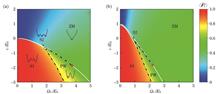
ObjectiveSpin?orbit coupling (SOC) links an atom’s spin angular momentum to its orbital angular momentum, leading to various novel physical phenomena. In Bose?Einstein condensate (BEC) systems, SOC modifies the dispersion relation, giving rise to exotic quantum phases in the ground state, which also exhibits rich collective excitation behavior. Floquet engineering is a powerful tool in quantum physics, enabling precise control over system parameters and manipulation of quantum states. Under high-frequency periodic driving, a spin?orbit coupled spinor BEC can be effectively described by a static effective Hamiltonian. In a spin-1 (spin quantum number is 1) system, periodic driving of the quadratic Zeeman field induces unconventional spin-exchange interactions, leading to new stripe phases. In this paper, we investigate the influence of Floquet high-frequency driving on the Rabi frequency by periodically modulating the Raman laser intensity. We explore the ground state phase transitions and collective excitations in this modulated spin-1 BEC system.MethodsTo analyze the ground state properties, we employ Floquet theory to derive the system’s effective Hamiltonian. First, we apply a unitary transformation to eliminate the time-dependent terms in the original Hamiltonian. Then, by averaging over one driving period, we obtain a time-independent effective Hamiltonian. To study the collective excitation properties, we use the Bogoliubov?de Gennes (BdG) method. By introducing perturbations to the ground state wave function, we construct the BdG matrix and extract the excitation properties of the system. We further analyze the density response function and static structure factor. In addition, we compute the sound velocity to compare with the ground state behavior.Results and DiscussionsThe obtained effective static Hamiltonian shows that both the SOC strength and the quadratic Zeeman field are modulated by the zero-order Bessel function of the first kind. Notably, the modulation introduces two distinct frequency components and a new spin operator F^y2, which emerge from the periodic driving of F^z2. Unlike quadratic Zeeman field modulation, Rabi frequency modulation does not generate new interaction terms, as rotational symmetry among spin operators in the interaction Hamiltonian remain intact. With the introduction of modulation, the boundaries of quantum phases in the ground state phase diagram shift (Fig. 1). The parameter space of the stripe phase S1 contracts along the Ω0 direction but expands into the positive range of the ε direction. The stripe phase S2 undergoes significant expansion. Given that in the absence of modulation, the stripe phase only appears when ε<0, the application of periodic driving extends the parameter range in which the stripe phase can be realized, particularly with respect to the quadratic Zeeman field. As modulation intensity increases, the plane wave phase contracts, while the zero-momentum phase expands. The effect of modulation on phase transitions is more pronounced when the constant Rabi frequency Ω0 is small (Fig. 2). In the excitation spectrum of the stripe phase, rotons appear when ε>0 (Fig. 3). As modulation intensity increases, the depth of roton minimum in each excitation band gradually decreases and shifts toward the center of the Brillouin zone. The energy gap between two lowest excitation bands widens, making atoms excitation less probable. At specific parameters where Ω0=1ER and ε=-1ER (Fig. 4), when modulation α /ω is weak, the ground state remains in the stripe phase. At the Brillouin zone boundary, both the structure factor and density response function exhibit divergence. Increasing modulation to α/ω=1.3 shifts the ground state to the plane wave phase. In this process, the roton mode in the excitation spectrum gradually vanishes. At roton position, the response function reaches maximum, while at the maxon position, the structure factor peaks. When α/ω=1.6, ground state transitions into the zero-momentum phase, where all excitation spectra exhibit symmetrical structures. Sound velocity is influenced by both modulation intensity and the constant Rabi frequency (Fig. 5). When α /ω is small, velocity remains largely unchanged. However, under strong modulation, velocity can vary significantly, particularly at phase boundaries. The larger the constant Rabi frequency, the more pronounced the velocity changes. Corresponding to the ground state, as modulation intensity changes, sound velocity undergoes phase transitions and exhibits distinct behaviors across different phases.ConclusionsIn this paper, we apply Floquet high-frequency driving on the Rabi frequency in a spin-1 spin?orbit coupled BEC to investigate ground state and collective excitation properties. Through a unitary transformation and averaging over one driving period, we obtain a time-independent effective Hamiltonian, in which both SOC intensity and the quadratic Zeeman field are modulated by the zero-order Bessel function. In addition, due to rotation symmetry, the interaction Hamiltonian remains unaffected by periodic driving. The ground state phase diagram varies with modulation intensity, and as modulation increases, phase transitions occur between the stripe, plane wave, and zero-momentum phases. Notably, the stripe phase extends into the positive region of the quadratic Zeeman field, thus allowing its observation over a broader parameter range in experiments. Through the BdG equation, we further obtain the excitation spectrum, density response function, and static structure factor, which provide key signatures for distinguishing quantum phases. Phase transition can also be characterized by sound velocity, where its continuity at phase boundaries reflects the transition type. In this paper, we demonstrate a novel method for controlling phase transitions through periodic modulation of the Rabi frequency, offering a more flexible approach to investigating the excitations and dynamics of spinor BECs.
May. 20, 2025Vol. 45 Issue 9 0902001 (2025)
Jun Qiu, Yuejing Qi, Jing Ma, Zhiyu Shi, Miao Jiang, and Jiangliu Shi
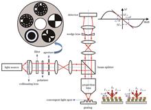
ObjectiveWith the continuous advancement of integrated circuit manufacturing technology and the reduction of device critical dimensions to nanoscale levels, high-precision overlay measurement has become a core challenge in photolithography technology. As the overlay label size gradually reduces and complex processing techniques are introduced, the aperture shape in angle-resolved scatterometer used for diffraction-based overlay (DBO) evolves from traditional annular apertures to BMW apertures and then to arch apertures, thus adapting to the constantly changing measurement needs. An optical characteristic model is constructed based on the principle of the angle-resolved scatterometer. On this basis, a simulation method for diffraction signals with different aperture shapes is proposed. The characteristics of the annular aperture, BMW aperture, and arch aperture are analyzed through theoretical analysis and simulation experiments. The performance parameter curves of overlay labels with different structural characteristics under different aperture conditions are calculated and compared. The applicable scenarios of each aperture are summarized, which provides a reference for aperture selection under various overlay label structures.MethodsTo analyze and compare the characteristics of different apertures, we propose a diffraction signal simulation method. Specifically, the shape of the converging light spot corresponding to different apertures is calculated through the Fourier transform. By sampling the pupil, we calculate the relationship between the wave vector components of the diffraction signal generated by incident light illuminating the label at various positions along the x, y, and z directions. This allows for the diffraction signal distribution at the back focal plane of the objective lens to be obtained. By combining rigorous coupled-wave analysis (RCWA), the intensity of diffraction signals at specific positions can be further calculated to determine the overlay performance parameters under different measurement conditions. The flowchart for diffraction signal distribution calculation is shown in Fig. 2. Using the proposed simulation method, the converging spot and diffraction signal distribution are simulated for different apertures, and the characteristics of each aperture are analyzed. The overlay performance parameters of conventional stacked overlay labels (Fig. 8) and multi-stacked overlay labels (Fig. 13) are simulated and analyzed under different aperture shapes and incident light parameters. Suitable scenarios for each aperture shape are provided based on the simulation results.Results and DiscussionsThe simulated converging spots and diffraction signal distributions corresponding to different apertures are shown in Figs. 5 to 7. The simulation results reveal that there is an overlap between the 0th-order and ±1st-order diffracted light signals of the annular aperture. The BMW aperture can achieve the separation of the 0th-order and ±1st-order diffraction signals. The arch aperture similarly offers the advantage of separating the 0th-order and ±1st-order diffraction signals, while the transparent area is the area with good uniformity of the diffraction signal in the BMW aperture. The curves of the performance parameters of conventional stacked overlay labels as a function of the incident light wavelength are shown in Figs. 10 to 12. The curves corresponding to the annular and BMW apertures are similar, with a maximum value higher than that of the arch aperture. However, there is an overlap between the 0th-order and ±1st-order diffraction signals of the annular aperture, which is not conducive to signal processing. It is recommended that the BMW aperture be prioritized for the overlay measurement of conventional stacked overlay labels. The curves of the performance parameters of multi-stacked overlay labels concerning the wavelength of incident light are shown in Figs. 14 to 16. Under most measurement conditions, the peak value of the curve of the arch aperture is higher than that of the other two types of apertures. It is recommended that the arch aperture be prioritized to achieve better measurement robustness and signal-to-noise ratio.ConclusionsBased on the principle of the angle-resolved scatterometer, we propose a diffraction signal simulation method for different apertures. Using this method, the characteristics of the annular aperture, BMW aperture, and arch aperture are analyzed. Through practical simulation cases, suitable scenarios for each aperture type are presented. The research concludes that for conventional stacked overlay labels, the performance parameter curves corresponding to annular and BMW apertures are similar, with a maximum value higher than that of the arch aperture. Considering the diffraction signal characteristics of apertures, it is recommended to prioritize using BMW apertures for overlay measurements. For multi-stacked overlay labels in the preparation of 3D devices, it is recommended to prioritize using arch aperture to achieve better measurement results. The simulation method and analysis results provide theoretical support and application references for the analysis and selection of aperture characteristics in angle-resolved scatterometer.
May. 20, 2025Vol. 45 Issue 9 0905001 (2025)
Chengwei Ma, Yu Zhou, Yuxin Jiang, Wei Lu, Zhiyong Lu, and Chaoyang Li
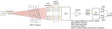
ObjectiveFree space optical communication (FSOC) features large broadband capacity, low cost, high security, small antenna size, small terminal size, and strong resistance to electromagnetic interference, with a wide range of application prospects. However, atmospheric turbulence can seriously affect the performance of satellite downlink laser communication systems. The array receiving system utilizes multiple smaller aperture receiving arrays to form a larger receiving aperture, improving beam coupling efficiency with the advantages of lower cost and more flexibility. The key to array reception lies in how to efficiently combine multiple received signals to improve the signal-to-noise ratio (SNR). Currently, there are mainly two methods of electrical beam combining and optical beam combining. The electrical beam combining method first detects the received signals of each aperture and then performs electrical merging. It requires detectors and signal acquisition processors corresponding to the number of channels, which is not conducive to high-speed communication. The optical beam combining method coherently synthesizes the received signals of each aperture in the optical device and then demodulates them by a single detector. Compared with electrical beam combining, it has a higher SNR but requires higher requirements for optical field regulation and control systems. Currently, there is relatively little research on this topic. Our study builds an optical coherent beam combining array receiving system model for typical satellite downlink communication and analyzes its performance by simulation. Based on the optical coherent beam combining method, a 10 aperture phased array laser communication receiver with equivalent aperture of 100 mm is built. We employ the rotating phase screen to simulate atmospheric turbulence, and complete coherent beam combining experiments and communication experiments, thus verifying the system performance.MethodsWe propose an optical coherent synthesis array receiving system model with a planar waveguide coupler structure, as shown in Fig. 1. Based on theoretical foundations such as atmospheric turbulence, fiber coupling, and optical coherent beam combining, we conduct a theoretical analysis of the system performance and simulate it under typical satellite downlink communication parameters. Meanwhile, we analyze the effects of the turbulence intensity, array aperture number, and receiving surface light intensity distribution on the bit error rate (BER) performance of the receiving system. Then, we conduct an array receiving coherent laser communication experiment, as shown in Figs. 7 and 9. Laser beams with wavelengths of 1550.12 nm and 1551.72 nm are loaded with communication signals at a rate of 56 Gbit/s by QPSK modulation, as shown in Fig. 12. After signal light amplification, it enters a simulated strong turbulent channel composed of a parallel light tube and a rotating phase screen. The channels of the array receiving system are preprocessed with equal optical path length, and after receiving the optical signal, the feedback control module performs optical coherent beam combining. Then, the optical power and coherent demodulation of the signal light are detected to obtain the system communication sensitivity.Results and DiscussionsFigures 2 and 3 show that as the equivalent optical SNR increases, the BER decreases to varying degrees at different aperture numbers. Under strong turbulence, the decrease becomes more significant with the rising aperture number. In Fig. 2, the required equivalent optical SNR decreases by about 2 dB for aperture numbers from 1 to 4 to achieve a 10-9 BER. In Fig. 3, the required equivalent optical SNR decreases by more than 6 dB in sequence to achieve the same BER, which is mainly due to the coupling efficiency improvement when the number of apertures increases. Additionally, spatial diversity technology itself can also improve the performance of the receiving system. However, as the number of apertures increases, the increase in coherent combination losses such as phase-locked losses will affect system performance, which makes the increment of SNR gain gradually decrease with the rising aperture number. Figure 4 shows the variation curves of the required SNR with the number of apertures for achieving a 10-7 BER at a zenith angle. It can be found that in this simulation condition, when the aperture number is greater than 10, the gain for increasing aperture number is no longer significant. Figure 5 reveals that with the increasing turbulence intensity, the fluctuation of the received optical power at each aperture increases, which has a greater influence on the amplitude of the combined beam signal. In the simulated parameter conditions, a maximum beam combination loss of 0.2 can be achieved. Under the zenith angle of 80°, this loss will increase the equivalent SNR requirement for eight-aperture reception by about 1 dB to achieve a BER of 10-9. In the experiment, the array beam phase is controlled by a feedback control system, and a combining efficiency of 0.587 is achieved after phase locking. However, due to factors such as phase screen turbulence disturbance, environmental vibration, and polarization, the beam combining efficiency is not very high and there are still some fluctuations in the light intensity after beam combining. The receiving optical power of -31 dBm is required for single wavelength 56 Gbit/s communication to achieve a receiving BER of 10-6. The receiving optical power of -27 dBm is required for dual-wavelength 112 Gbit/s communication, and its receiving sensitivity is about 10 dB away from the shot noise limit. Additionally, we conduct system reliability experiments. The experimental results are shown in Fig. 14. At a dual wavelength communication rate of 112 Gbit/s, when the received power is -23 dBm to -26 dBm, the laser link is built for 17 min, and the system availability is 99.77%. This demonstrates the high reliability of the communication system.ConclusionsWe study the performance of suppressing strong turbulence in an array receiving coherent laser communication. For a typical satellite-to-ground downlink communication link, an optical coherent synthetic array receiving system model is built. Numerical simulations are conducted to analyze the variation of the system BER with equivalent SNR under different aperture numbers and turbulence intensities. The results show that increasing the number of apertures can improve system performance, especially in strong turbulence conditions. The aperture number increase significantly enhances fiber coupling efficiency, thereby improving the system's tolerance to beam combining loss. Additionally, the effect of random intensity variations on the amplitude of the beam-combined signal and equivalent SNR is analyzed. In the simulation conditions, when the zenith angle is 80°, the loss requires an increase of approximately 1 dB in the equivalent SNR for an eight-aperture receiver to achieve a BER of 10-9. Meanwhile, a 10-aperture array laser communication receiver is constructed. In the laboratory environment, we simulate the turbulence environment with r0=4 cm by employing the rotating phase screen and conduct beam combining and communication experiments, thus achieving phase lock efficiency of 0.587, communication reception sensitivities of 10-6@-31 dBm&50 Gbit/s and 10-6@-27 dBm&100 Gbit/s,and availability of 99% for long-term chain building. This proves the feasibility and application potential of the array receiving and optical combining system in strong turbulent communication environments. In the future, we will further control the optical path difference of the array to improve its performance in multi-wavelength communication and conduct out-field experiments to demonstrate its communication effectiveness in the real atmosphere.
May. 16, 2025Vol. 45 Issue 9 0906001 (2025)
Dexu Kong, Yongwei Xia, Renlong Zhang, Rong Long, Yufei Zhang, and Qiang Liu
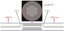
ObjectiveStrain sensors can convert mechanical deformation into light/electrical signals and play an important role in fields such as robotics, human-computer interaction, electronic skin, human health, aircraft structures, and ground deformation monitoring. Fiber optic sensors offer many outstanding advantages, such as electromagnetic interference resistance, corrosion resistance, miniaturization, fast response speed, remote operation, and real-time monitoring. These sensors are a unique sensing method in specific situations, such as electrical hazards and explosive environments. Based on the above advantages, optical fiber sensors have great potential and application value in the field of strain detection. Photonic crystal fibers (PCF) have characteristics that traditional fibers do not possess. First, while traditional fibers are typically made of solid material, PCFs contain many pores, which makes it easier to deform when subjected to mechanical forces. Therefore, strain sensors based on PCF are more sensitive. Second, the background material of the PCF consists of pure silica and air holes, which results in very low thermal dependence. This helps to avoid crosstalk between strain and temperature, as the thermal sensitivity coefficient of the core in traditional optical fibers is much higher than that of pure silica due to the doping of other materials. Numerous reports on strain sensors based on PCFs exist, and their sensing types mainly include Fabry?Perot interferometers, Mach?Zehnder interferometers, Sagnac interferometers, long-period gratings, mode coupling, and others. These sensors are typically used as single-point sensors. By connecting multiple sensors in series to form a sensor array, a single interrogation unit can measure multiple sensing points simultaneously. This approach can significantly reduce the cost and complexity of sensors and enable the creation of sensor networks.MethodsThe PCF used in this experiment consists of six layers of air holes arranged in a hexagonal pattern. Compared with ordinary single-mode PCF, it has more air holes. Although it is also a refractive index-guided PCF, the more complex cladding structure can excite higher-order modes, which enables the interferometer to have a richer output spectrum. The welding model number is FITEL s179c. Since there is no welding procedure set for this type of PCF in the welding machine, the welding of the single-mode fiber and PCF is completed manually. The preparation of the interferometer involves only simple cutting and welding, which can be done using cutting knives and welding machines. The main preparation steps are as follows: before welding, remove the coating layer of the fiber and wipe it with alcohol; place the PCF and single-mode fiber at both ends of the welding machine, align them manually, and select the appropriate discharge intensity for welding. The porous structure of the PCF collapses under the stimulation of a high-intensity current to form a solid silicide. Light is introduced from the left end of the single-mode fiber, then into the solid silicide. The light is diffracted and broadened in the silicide, then enters the core and cladding of the PCF, meeting at the collapse region at the other end of the PCF, where it is coupled to form Mach?Zender interference. The position and depth of the valley are closely related to the length of the collapse area. A deeper valley improves the contrast and is more conducive to the detection of the sensor. The optical fiber sensor with different valley positions is obtained by tuning the length of the collapse area, and then the sensor is cascaded to realize the optical fiber sensor array.Results and DiscussionsThe total output spectrum of the three interferometers after cascading is a simple superposition of the output spectrum of each individual interferometer (Fig. 6), and the position of the resonance wavelength remains basically unchanged. As shown in this figure, the valleys of the three PCF interferometers are effectively separated, and the spacing between them is relatively large, which means that a sufficient range of spectrum movement is available. This provides the basis for the sensor to measure multiple sets of parameters or multiple points simultaneously. We perform strain experiments on the cascaded interferometers. First, the total strain applied to the interferometer with a PCF length of 10.5 mm is 1800 με, with a strain interval of 300 με. The corresponding valley of the 10.5 mm interferometer lies within the range of 1570?1600 nm, and the interference valley shifts to shorter wavelengths as the strain increases. Meanwhile, the valleys of the other two PCFIs remain almost unchanged, which indicates that the spectral movement caused by the detection of the interferometer does not affect the detection of the other two interferometers [Fig. 7(a)]. The relationship between the valley of the three interferometers and the strain is shown [Fig. 7(b)], and the valley corresponding to the 10.5 mm interferometer is fitted linearly. The linear fitting coefficient reaches 0.99905, the fitting equation is y=-0.00143x+1585.11, and the sensitivity is -1.43 pm/με. The other two valleys shift by up to 0.042 nm. From the results of the measurements and linear fitting, the cascaded use of the interferometer does not affect its own performance or measurement accuracy. We conduct a similar experiment on another interferometer and obtain similar results, where the wavelength corresponding to the valley of the interferometer shifts towards shorter wavelengths as the strain increases, and the sensitivity reaches -1.55 pm/με. The difference in interferometer length leads to differences in sensitivity, while the valley positions of the other two interferometers, which are not subjected to strain, change very little.ConclusionsWe present an interferometric fiber sensor formed by fusing a PCF into two single-mode fibers. Strain is measured by observing the movement of the spectrum. By optimizing the collapse region length of the PCF, the appropriate cladding and core modes are excited. This coupling results in a narrow and deep valley appearing across a wide wavelength range, which greatly reduces the difficulty of sensor cascading and demodulation. An interesting phenomenon is observed during the experiment: when the input and output terminals are connected in a positive-negative configuration, the spectrum waveform remains almost unchanged. We first perform strain experiments on a single sensor, which shows a sensitivity of -1.36 pm/με and a linearity of 0.98920. Then, we conduct strain experiments on the cascaded PCF interferometer. There is almost no crosstalk between the sensors, which indicates that simultaneous measurement of different parameters or multi-point measurement of the same parameter could be realized. With further study of optical fiber mode excitation, we anticipate that the sensor’s loss will be reduced, and the number of sensors in the array will increase, thereby expanding the application potential of optical fiber sensors.
May. 20, 2025Vol. 45 Issue 9 0906002 (2025)
Jingli Wang, Chufan Li, Hongdan Wan, and Heming Chen
ObjectiveHigh birefringence terahertz fibers have a strong polarization preservation ability for linearly polarized light. They can be used for polarization-maintaining transmission of terahertz waves, polarization control, and modulation of terahertz signals. Currently, the most common high birefringence terahertz fibers include photonic crystal fibers and hollow core anti-resonant fibers (HC-ARFs). The former generally introduces structural asymmetry by arranging air holes or changing the core shape to achieve mode birefringence (B). However, their structures are relatively complex, leading to higher fabrication difficulties and significant effective material losses. The latter utilizes the anti-resonant reflection effect for light guidance, which results in low confinement loss and a simple structure. This not only simplifies the fabrication process but also minimizes effective material loss, which makes it a focal point of current research. However, most of the reported high birefringence terahertz HC-ARFs fail to achieve both high mode birefringence and low loss across a broad bandwidth. Based on this, a new structure is designed for high birefringence terahertz HC-ARF. This design combines the introduction of non-circular tubes and nested structures in the cladding. Additionally, four gap-compensated circular tubes are introduced, and high-resistivity silicon with low absorption loss is used as the fiber material to further reduce transmission loss (TL) and improve fiber performance.MethodsFirstly, we present the design of the structure for a high birefringence terahertz HC-ARF. Nested structures are incorporated in both the x and y directions, and non-circular tubes are introduced within the cladding tubes to induce asymmetry in the fiber structure, thereby achieving high birefringence. Secondly, four gap compensated circular tubes are added to the interstitial spaces within the cladding tubes, with the aim of reducing confinement loss in the fiber. Furthermore, high resistivity silicon is selected as the fiber material to minimize the effective material loss within the fiber. Subsequently, the control variable method is used to optimize the fiber structure parameters, including the outer diameter of the circular tube in the y-direction (d1), the outer diameter of the nested circular tube in the y-direction (d2), the major axis of the outer elliptical tube in the x-direction (d3), the ellipticity η, the major axis of the nested elliptical tube in the x-direction (d4), the outer diameter of the gap compensated circular tubes (d5), and tube thickness t. The objective is to achieve optimal values for both the TL and the B of the fiber. Finally, based on the optimal structural parameters of the fiber, within the frequency range of 0.7 to 1.4 THz, the properties of the fiber are analyzed such as TL, B, and dispersion.Results and DiscussionsFirstly, a high birefringence terahertz HC-ARF is designed in this paper. On one hand, high birefringence is achieved by incorporating non-circular tubes and nested structures within the cladding tubes. On the other hand, the introduction of four gap compensated circular tubes in the interstitial spaces of the cladding tubes reduces confinement loss. Additionally, the use of high resistivity silicon materials further decreases the effective material loss (Fig. 1). Secondly, at an operating frequency of 1 THz, the structural parameters of the fiber are optimized. The results show that the best TL and B are achieved with d1=3.0 mm, d2=1.0 mm, d3=3.1 mm, η=0.525, d4=d2=1.0 mm, d5=1.2 mm, and t=0.035 mm. Next, we analyze the properties of the fiber, such as TL, B, and dispersion, within the frequency range of 0.7 to 1.4 THz. The results indicate that within the bandwidth ranging from 0.92 to 1.32 THz, B exceeds 1.09×10⁻³ [Fig. 8(a)]. TL remains as low as 1 dB/m, with the minimum transmission loss of 0.09 dB/m occurring at a frequency of 1.18 THz. Finally, the dispersion performance of the fiber is simulated and analyzed. The results show that in the bandwidth of 0.92 to 1.32 THz, the designed high birefringence terahertz HC-ARF exhibits near-zero and flat waveguide dispersion, with a dispersion variation of (0.13513±0.22014) ps-1·THz-1·cm-1 (Fig. 9). Meanwhile, the lowest polarization mode dispersion of 3.68×10⁻¹² s is achieved (Fig. 10).ConclusionsIn this paper, we design a high birefringence terahertz HC-ARF with both high B and low TL across a wide bandwidth. To accomplish this, we incorporate non-circular tubes into the cladding, introduce nested structures in both the x and y directions, and incorporate gap-compensated circular tubes within the cladding gaps. The results demonstrate that, within the bandwidth ranging from 0.92 to 1.32 THz, the high birefringence terahertz HC-ARF exhibits B greater than 10-3 and TL as low as 1 dB/m. Notably, the lowest transmission loss is achieved at a frequency of 1.18 THz, where the TL for the x-polarization mode is 0.14 dB/m and the TL for the y-polarization mode is 0.09 dB/m. Additionally, it possesses excellent dispersion characteristics. This fiber has broad prospects in areas such as polarization-maintaining transmission of terahertz waves and polarization control of terahertz signals. It also provides a reference for the design of high birefringence terahertz fibers.
May. 16, 2025Vol. 45 Issue 9 0906003 (2025)
Rui Huang, Qinghua Tian, Zuxian Li, Yiqun Pan, Fu Wang, Feng Tian, Sitong Zhou, Yongjun Wang, and Xiangjun Xin
ObjectiveWith the development of optical communication technology towards higher capacity, speed, and bandwidth, the phase noise caused by laser linewidth is becoming one of the key factors limiting the spectral efficiency of the system. Especially in high-order modulation formats, the tolerance of the system to phase noise gradually decreases, and excessive residual phase noise can lead to significant degradation in system performance. Meanwhile, with the increase in baud rate and transmission distance, the influence of equalization-enhanced phase noise (EEPN), generated by the interaction between the phase noise of the local oscillator laser at the receiver and the dispersion compensation module, gradually increases. Therefore, it is of great significance to accurately compensate for the phase noise. Currently, algorithms for carrier phase recovery include Viterbi?Viterbi phase estimation (VVPE) and blind phase search (BPS). VVPE is simple to implement, but for multi-level modulation formats, constellation partitioning must be carried out before implementation, which introduces an implementation penalty due to decision errors. BPS offers good compensation performance and is applicable to multiple modulation formats, but it consumes significant computational resources, as it requires numerous test phases and a sliding window with a large block size to estimate phase noise and smooth linear noise. We propose a phase noise compensation scheme based on end-to-end deep learning (E2EDL). This scheme learns the influence of phase noise on the signal, enhances the robustness of the system to phase noise and dispersion through constellation shaping, and improves the ability of the algorithm to track phase noise through a trainable BPS, thus enhancing the phase noise compensation performance.MethodsA phase noise compensation scheme based on E2EDL is proposed to compensate for phase noise, including EEPN generated by the interaction between dispersion and phase noise, from multiple aspects. This scheme uses E2EDL for constellation shaping, including both geometric shaping and joint geometric-probabilistic shaping, to improve the tolerance of the system to phase noise. Meanwhile, a trainable BPS is proposed. The non-differentiable comparison operation in traditional BPS is replaced by a differentiable soft decision, which is abstracted as a neural network. Using the characteristics of E2EDL, the standard deviations of AWGN and Wiener phase noise are added and then incorporated into the E2EDL framework for overall training, thus improving its compensation ability for phase noise. In addition, the photonic Sigmoid function in optical computing is incorporated into the E2EDL framework for coherent optical communication. Utilizing its ability to simulate the physical response of photon devices, the tolerance of the system to dispersion is enhanced, and the compensation ability of BPS for EEPN is improved by reducing the influence of dispersion.Results and DiscussionsNumerical simulations are carried out on channels containing only dispersion, phase noise, and AWGN, as well as on channels containing nonlinear effects, respectively, to verify the performance of the proposed scheme. Additionally, simulation analyses are performed to evaluate the performance differences between the proposed scheme, the traditional QAM modulation scheme, and the E2E (no CD) scheme, which only learns the phase noise channel, under different laser linewidths. On the channel containing only dispersion, phase noise, and AWGN, when the laser linewidth changes within the range of 0 to 600 kHz, the generalized mutual information (GMI) performance of the proposed scheme in both geometric shaping and joint shaping is higher than that of E2E (no CD). The simulation analysis also studies the bit error rate curves of the proposed scheme and the traditional 64QAM scheme under different optical signal-to-noise ratios (OSNR). In the case of low OSNR, the proposed scheme demonstrates stronger robustness to amplified spontaneous emission noise and shows more clear advantages compared with the traditional 64QAM scheme. At a bit error rate standard of 3.8×10⁻³, the proposed scheme achieves an OSNR gain of about 0.6 dB compared with the traditional 64QAM. Under the channel with nonlinear effects, at the optimal transmit power, the proposed scheme provides a Q-factor improvement of about 0.44 dB compared to the traditional 64QAM scheme. Finally, we analyze the GMI performance of the three schemes under different laser linewidths at 800, 1040, and 1200 km. The GMI performance of the proposed scheme is higher than that of E2E (no CD) at different transmission distances. The proposed scheme improves the tolerance and compensation ability to phase noise by learning the interaction between phase noise and dispersion in the channel, thus improving the performance of the scheme under the influence of phase noise.ConclusionsWe propose a phase noise compensation scheme based on E2EDL. This scheme enhances the system’s ability to compensate for phase noise by learning the interaction between phase noise and dispersion in the channel, as well as conducting constellation shaping and BPS training. Compared with the traditional 64QAM+BPS, the proposed scheme provides an OSNR gain of approximately 0.6 dB in the case of 1200 km transmission. In addition, it incorporates the photonic Sigmoid activation function to reduce the influence of dispersion, further improving the performance of the system in the presence of dispersion. The performance of the proposed scheme is verified through numerical simulations. In the case of low SNR and large laser linewidth, the GMI performance of 64QAM is improved by about 0.17 bit/symbol, providing an additional gain of about 0.07 bit/symbol compared with E2E (no CD). In the presence of nonlinear effects, this gain increases further, reaching 0.59 bit/symbol and 0.17 bit/symbol, respectively. At the optimal transmit power, the Q factor of the proposed scheme improves by approximately 0.44 dB compared with the traditional 64QAM scheme.
May. 20, 2025Vol. 45 Issue 9 0906004 (2025)
Ting Yan, Chaoliang He, Qian Tong, Songtao Zhu, and Xiaojiao Duan
ObjectiveCone-beam computed tomography (CBCT) has been widely used in various fields such as industrial measurement, security inspection, and medical imaging. However, during the CT scanning process, the Compton effect inevitably leads to issues in CT images, including scatter artifacts, reduced image contrast, and information loss. Compared with other types of scanning methods, CBCT has a larger cone angle and detector area, which allows it to receive more scattered photons, thus being more severely affected by scatter. As a result, effective methods need to be adopted to perform scatter correction on CBCT images, restore image quality, and improve the accuracy of clinical diagnosis.MethodsTo achieve CBCT scatter correction, we design a novel dual-encoder network model, DEU-Net. DEU-Net is composed of a densely connected convolutional neural network (DCCNN) module and a Swin transformer (Swin-T) module. These two modules are utilized to extract local and global features of the image and combine them to achieve preliminary image correction in the image domain. Based on the low-frequency characteristics of scatter, the DEU-Net model is combined with a two-dimensional discrete wavelet transform. Scatter information is extracted in the projection domain to achieve final scatter correction. A weighted loss function is designed to ensure that the model training process focuses more on the parts of the image with complex structures and large errors, thereby obtaining better correction results.Results and DiscussionsThe feasibility and effectiveness of this method are verified using the MC dataset, which is composed of pelvic data and high- and low-dose data. The comparison results before and after correction are shown in Fig. 5. The proposed method is compared with other deep learning-based methods, and the results are presented in Fig. 6, with the indicator data shown in Table 1. It is evident from the results that, compared with other correction methods, the method proposed in this paper has the smallest CT difference and the best correction effect. The corrected CT images exhibit higher contrast, which makes the distinction between different tissue structures more obvious. Moreover, ablation experiments are conducted to verify the positive effects of each module on the correction results (Fig. 7 and Table 2). The proposed method can also achieve excellent results in correcting scatter in low-dose CT images (Figs. 10 and 11, Tables 3 and 4). This demonstrates its potential clinical values in restoring image quality and data accuracy and realizing scatter correction. In addition, this method is used to correct and analyze the CT images of turbine blades to verify its ability to correct real scatter artifacts. The results are presented in Fig. 13, as well as Tables 5 and 6. The CT images corrected by the method in this paper are cleaner, the scatter artifacts are better suppressed, and the grayscale distribution of the object part is more uniform.ConclusionsDuring the CBCT and imaging process, the Compton effect affects the quality of the reconstructed image, thus leading to phenomena such as scatter artifacts and inaccurate CT values. We propose a novel DEU-Net structure to achieve preliminary scatter correction in the image domain. Moreover, based on the low-frequency characteristics of scatter, the output of the model is combined with two-dimensional discrete wavelet transform to extract the low-frequency scatter signal in the projection domain, thereby realizing the final scatter correction of CBCT images. In this network structure, the two encoding paths serve different purposes. DCCNN module is used to extract local features of the image, while Swin-T module is used to extract global features. These two modules complement each other, thereby enhancing the model’s feature extraction ability and improving the correction effect. In addition, a new weighted loss function is designed to ensure that the model training process gives more attention to the parts of the object with complex structures. The experimental results show that the method combining the dual-encoder network model with wavelet transform can effectively perform scatter correction, improve the quality of CBCT images, and has the potential to enhance the accuracy of radiotherapy diagnosis in clinical practice. Meanwhile, applying this method to perform scatter correction on the CT images of aero-engine turbine blades verifies its ability to correct real scatter artifacts.
May. 16, 2025Vol. 45 Issue 9 0910001 (2025)
Yulan Han, Deao Chen, Tong Wu, Xianlu Liu, and Chaofeng Lan
ObjectiveThe rapid advancement of intelligent transportation systems has increased the demand for precise and swift traffic object detection capabilities, particularly under challenging low-light conditions and complex backgrounds. Infrared (IR) imaging technology has emerged as a critical tool for such scenarios due to its ability to capture heat signatures, thus enabling reliable detection even in darkness or through obscurants. However, traditional IR detection methods are often hindered by high computational complexity, large parameter sizes, and dependency on high-performance computing resources, which makes them unsuitable for deployment on resource-limited mobile devices. We introduce the Edge-DETR network, specifically designed for the efficient and accurate detection of traffic objects in IR imagery on edge devices.MethodsThe Edge-DETR network is an innovative detection framework that builds upon the RT-DETR model with several enhancements. It incorporates a context anchor attention multistage efficient layer aggregation network (CAA-MELAN) to adaptively extract multi-scale features and understand global dependencies, thereby addressing the challenges posed by varying object sizes and environmental dynamics. Additionally, a global information supplement module (GISM) is employed for effective feature downsampling, which ensures the preservation of essential spatial information while reducing computational load. The cross-level feature fusion module (CFFM) facilitates interaction among features at different scales, enhancing the network’s capability to integrate high-level semantic information with low-level spatial details. The HiLo attention mechanism is introduced to optimize intra-scale feature interaction, with a focus on target contours while minimizing parameter and computational requirements. To address the detection of objects with complex shapes and sizes, a Shape-IoU loss function is utilized, which accounts for the shape and size of bounding boxes in the loss calculation. Extensive experiments are conducted across multiple datasets, including FLIR, KAIST, LLVIP, and a self-built dataset, to comprehensively evaluate the network’s performance.Results and DiscussionsThe Edge-DETR network demonstrates superior performance across various datasets, significantly outperforming similar methods in terms of detection accuracy and computational efficiency. Compared to the RT-DETR model, our network achieves a 46% reduction in parameters and a 39% decrease in floating point operations (FLOPs), with the model size compressed by 45%, down to 21 MB. The network’s accuracy is particularly notable for detecting small targets and in complex scenarios, significantly reducing false positives and missed detections. Fig. 1 illustrates the network model, showcasing its structural components, while Fig. 6 presents the heatmaps of detection results, indicating the network’s precision in target contour detection despite the reduction in parameters and FLOPs. The ablation study results, as shown in Table 1, further validate the contribution of each component to the overall network performance, with the combined model showing the best detection accuracy. The network’s performance in terms of precision is also superior, as evidenced by the high mAP scores achieved across different datasets. Detailed analysis of the results reveals that the CAA-MELAN module significantly enhances feature extraction capabilities, particularly for small and rectangular targets commonly found in traffic scenes. The CFFM’s ability to fuse features across different scales provides a more comprehensive understanding of the scene, leading to improved detection accuracy. The HiLo attention mechanism effectively balances the trade-off between computational efficiency and detection accuracy, while the Shape-IoU loss function fine-tunes the network to better handle the complexities of real-world traffic scenarios. We also observe that the network’s performance is robust across different weather conditions and lighting environments, which is crucial for real-world applications.ConclusionsThe Edge-DETR network has proven its effectiveness for IR object detection on edge devices, striking a balance between detection accuracy and computational efficiency. Its ability to adapt to different scales and contexts, coupled with a lightweight computational footprint, positions it as a leading solution for edge device deployment in traffic object detection scenarios. The success of this network lies in its innovative approach to feature extraction and fusion, which allows for a detailed understanding of the traffic environment while maintaining low resource consumption. The Edge-DETR network’s performance under various conditions, including different lighting and weather scenarios, suggests that it can provide consistent detection capabilities, which are essential for safety-critical applications. Its scalability also means it can be adapted to different levels of complexity in traffic scenarios, from simple urban settings to complex highway environments. This flexibility, combined with efficiency, makes the Edge-DETR network a promising candidate for integration into a wide range of transportation systems. As we continue to develop and refine this technology, we anticipate that it will play a crucial role in enhancing the safety and efficiency of transportation networks worldwide. The Edge-DETR network’s success in handling the nuances of IR imagery also opens up possibilities for its application in other domains where IR detection is critical, such as military surveillance, search and rescue operations, and industrial automation. Overall, the Edge-DETR network’s performance metrics, versatility, and potential for integration into existing and future systems make it a standout solution in the field of edge computing for traffic object detection.
May. 20, 2025Vol. 45 Issue 9 0910002 (2025)
Xiaoqing Tian, Bao Liu, Qiang Guo, and Hongguang Pan
ObjectiveIn contrast to common data modalities such as visible light and infrared, hyperspectral images inherently offer advantages and stronger characteristics in target tracking tasks, holding great potential for applications in complex environments and scenarios. However, on the one hand, most improved correlation filter (CF) methods extract target features solely from spectral or false-color images, thereby resulting in insufficient target feature description. On the other hand, during the training process of spatially/temporally regularized correlation filters, such as kernelized correlation filter (KCF) and background-aware correlation filter (BACF), the varying sensitivity of different channels to background noise changes and the similarity of background features between adjacent frames are often overlooked. This leads to inadequate utilization of channel information and background environmental changes. These factors contribute to the decreased performance of CF algorithms when tracking targets in scenes with rapidly changing backgrounds, and tracking drift may even occur. To address the poor tracking performance of existing hyperspectral video tracking algorithms in scenarios with rapidly changing backgrounds, we propose an efficient correlation filter-based tracking algorithm to achieve robust tracking of moving targets in such environments.MethodsAn environmental residual-aware (ERA), multi-regularized correlation filter (MRCF) tracking algorithm is proposed in this study. First, to reduce computational complexity, a background-aware band selection method is employed to select three bands from multi-band hyperspectral images. The selected three-band images, characterized by the top three highest dissimilarity scores between the target and its local neighborhood, are formed into a three-channel spectral image for target tracking. Secondly, three typical features of the target in the false-color image and three-channel spectral image are extracted: histogram of oriented gradients (HOG), intensity, and 3D HOG features. These target features from the false-color image and the three-channel spectral image are fused by simply adding them in a naive manner to obtain the fused feature, thereby enhancing the ability to represent the target. Finally, the fused target feature is used as input for the improved MRCF to predict the target position. In the training stage of the CF, an ERA regularization term is introduced into the ridge regression optimization function of MRCF to suppress interference caused by rapid background changes.Results and DiscussionsTo verify the effectiveness of the proposed algorithm, we select four hyperspectral target tracking algorithms and compare them in the experiment. Meanwhile, we select three specific sequences from the test set to visualize the performance of the proposed algorithm in comparison with the other four algorithms. We evaluate the algorithms from two aspects: tracking accuracy and success rate. Figure 3 shows the precision and success rate curves of each algorithm on the test sequence. Figures 4 and 5 demonstrate the precision and success rate in the presence of fast target motion and scale variation challenges. As shown in Fig. 3, the proposed algorithm ranks first in terms of precision and success rate on the total test sequence. Specifically, the precision increases by 2.51%, and the success rate grows by 1.67% compared to MHT. Due to the joint utilization of feature fusion and ERA regularization modules, the algorithm exhibits strong robustness. As shown in Fig. 4, in the case of tracking a target with fast motion, the precision and success rate of the proposed algorithm are much higher than those of the second-place algorithm. This occurs as the two modules—false-color/spectral feature fusion and ERA regularization—collaboratively reduce the effect of background changes between adjacent frames on the tracker, in terms of feature representation and filter training. Additionally, as shown in Fig. 5, under the challenge of scale variation, the precision and success rate of the proposed algorithm are 6.24% and 2.52% higher than those of the second-place algorithm, respectively, demonstrating excellent adaptability. Fig. 9 shows the qualitative analysis results of various algorithms in the selected sequences. In the Droneshow2 sequence, a small-sized UAV with low contrast against the surrounding background is flying from right to left. Since the proposed algorithm enhances its discriminative capability for small targets by using fused features from false-color/three-band spectral images, it can successfully discern the location of the UAV. In the L~~car2 sequence, a person is walking from near to far, with variations in both target scale and background environmental information occurring during the process. The proposed algorithm incorporates a background ERA regularization term to effectively adapt to variations in the background environment and achieve tracking robustness. Table 2 presents the precision and success rate of the ablation experiment and reveals that the proposed method improves the algorithm’s robustness.Conclusions1) To address the issue of insufficient target feature description, which leads to inadequate target discrimination ability in hyperspectral object tracking tasks, we employ a fusion method based on the simple addition of features from false-color images and three-band spectral images. This method effectively balances the retention of details from each feature while reducing the effect of background or interfering features, thereby enhancing the representation capability of hyperspectral target features. 2) Furthermore, to tackle the problem of insufficient utilization of channel and background environmental change information, which leads to decreased tracking performance in rapidly changing background scenarios, we propose an ERA-MRCF. The proposed algorithm incorporates an ERA module within the MRCF framework, which, while preserving MRCF’s robust perception of target appearance changes, suppresses the interference caused by rapid background changes. This enhancement improves the tracker’s robustness in challenging scenarios such as fast target motion. Experimental results on the public hyperspectral datasets HOTC2024 and IMEC25 validate the algorithm’s excellent tracking performance in terms of fast motion and scale variation. 3) Future work will focus on improving band selection methods and feature representation for small hyperspectral targets. This includes not only fully exploring the fused feature representation for small targets, such as employing weighted fusion based on both overlap ratio and distance reliabilities, as well as deep learning-based multi-modality feature fusion to enhance the tracker’s ability to discriminate small targets, but also refining band selection methods to go beyond merely utilizing the dissimilarity information between the target and its surrounding background in the current frame. Additionally, efforts will be made to design intelligent fusion strategies for detection and tracking results to improve the algorithm’s robustness against occlusion.
May. 16, 2025Vol. 45 Issue 9 0910003 (2025)
Xiuyue You, Yi Tang, Lijun Zhang, and Dongxiao Wang
ObjectiveThe luminance variation in natural scenes is extremely wide, whereas traditional cameras have a limited dynamic range. High dynamic range (HDR) imaging technology overcomes this limitation by preserving scene details more accurately, maintaining highlight information while enhancing shadow details, thus comprehensively retaining scene information. Consequently, HDR technology has been widely applied in digital photography, medical imaging, satellite remote sensing, and video production. Extensive research has been conducted globally on HDR fusion algorithms, with representative methods including entropy-based block fusion, tri-segment linear fitting, multi-exposure nonlinear fusion, and deep learning approaches. However, existing studies still suffer from high algorithmic complexity, poor real-time performance, and low resolution. We propose a fast HDR fusion method based on a large-area dual-channel scientific complementary metal oxide semiconductor (sCMOS) sensor. Using an field-programmable gate array (FPGA) as the core controller, we design a high-dynamic-range large-area real-time imaging system, along with HDR application strategies tailored to different scenarios. The system consumes minimal hardware resources, features a simple algorithm, and achieves superior imaging performance. It integrates the advantages of high-resolution and high-dynamic-range imaging, providing valuable insights for the design of similar instruments.MethodsWe focus on the principle of fast HDR fusion and the integrated design of an FPGA-based imaging system. The dual-channel sCMOS sensor incorporates two amplifiers per pixel column, enabling simultaneous output of high-gain (HG) and low-gain (LG) images in a single exposure. The core principle of the HDR fusion method lies in leveraging the differences in photoresponse characteristics: in high-intensity illumination conditions, the HG image becomes overexposed and saturated, necessitating the use of LG data to preserve highlight details. Conversely, in low-intensity conditions, the LG image exhibits generally lower grayscale values, requiring the HG image to capture shadow details. First, the HG and LG photoresponse curves are precisely calibrated and parameterized to derive a linear fusion function. Subsequently, an FPGA with a DDR3-based hardware architecture is utilized to integrate on-chip image acquisition, fast HDR fusion, image storage, and transmission. To address the challenges of large-area, high-bit-width data transmission, a shift-based segmented transmission mechanism and an alternating-frame transmission strategy are proposed. Finally, the system is developed and evaluated through experimental tests, demonstrating the effectiveness of HDR fusion. Application strategies for different lighting conditions are proposed: a high-gain-dominant fusion method is adopted for low-light scenarios, whereas a low-gain-dominant fusion method is employed for high-light-intensity environments.Results and DiscussionsThe designed high-dynamic-range large-area real-time imaging system consumes minimal hardware resources (Table 1), achieves an imaging resolution of 4096 pixel×4096 pixel with 16 bit depth, and extends the grayscale value from 4095 to 65535 (Fig. 8), combining the advantages of large-area cameras and high-dynamic-range imaging. Experimental results show that the proposed fast HDR fusion method requires the shortest processing time of only 35 ms compared to three-segment curve fitting algorithm and information entropy block fusion algorithm while maintaining superior HDR imaging performance (Fig. 10), with 8.5% and 14.1% increase in image entropy (Table 2). Furthermore, scenario-specific HDR strategies are proposed (Fig. 13): for low-light conditions (Fig. 14), a high-gain-dominant fusion method is employed, whereas for high-light conditions (Fig. 15), a low-gain-dominant approach is applied to achieve optimal HDR effects across diverse environments.ConclusionsThe advantages of large-area cameras and high-dynamic-range imaging are integrated into this paper through the design of a high-dynamic-range large-area real-time system. Based on the large-area dual-channel sCMOS sensor GSENSE4040BSI, a fast HDR fusion method is proposed alongside scenario-specific HDR strategies. To address the challenges of large-area image data transmission, a shift-based segmented transmission method, and a dual-channel alternating-frame transmission mechanism are introduced. A complete real-time imaging system is developed: first, the HG and LG photoresponse curves of the sCMOS sensor are tested and calibrated to derive a linear fusion function. Then, on the FPGA hardware platform, on-chip integration of image acquisition, fast HDR fusion, image storage, and transmission is achieved. Ultimately, a 4096 pixel×4096 pixel HDR real-time system with a maximum frame rate of 24 frame/s is implemented. The proposed algorithm is simple yet effective, requiring only 35 ms for processing, demonstrating high real-time performance, and extending the pixel bit depth from 12 bit to 16 bit. It successfully preserves both highlight and shadow details, improving image entropy by 11.3% compared to other algorithms. The system satisfies real-time imaging demands for high dynamic range and high resolution. Further development may target higher frame rates, miniaturization, and self-adaptive HDR mechanisms.
May. 16, 2025Vol. 45 Issue 9 0911001 (2025)
Heng Zhao, Shiyu Ge, Sipu Zhang, Yao Zhang, Yanyan Zhang, Jiamin Fang, and Dengxin Hua
ObjectiveThe rapid pace of industrialization and urbanization has led to increasing concerns about air particulate pollution, which is now a major factor influencing quality of life and public health. Airborne particulate matter not only harms the respiratory system but also acts as a carrier for various pollutants. Long-term exposure to particulate pollution significantly raises the risk of respiratory diseases, cardiovascular issues, and even cancer. Furthermore, the effect of particles on human health is linked to their size, with smaller particles posing a greater risk. Therefore, we aim to design a T-type optical particle separation (TOPS) chip based on optical flow control technology to sort particles of different sizes. This research is crucial for advancing our understanding of the sources, transmission, and transformation mechanisms of atmospheric aerosol particles, as well as for developing effective prevention and control measures.MethodsWe investigate the behavior analysis and experimental validation of aerosol particles based on TOPS technology. First, in the sorting microchannel, the particle motion is simplified as a motion under a constant force field, considering both radiation and fluid drag forces. We derive a formula for the constant scattering force on spherical particles, which leads to the particle motion control equation. From this, the formula for the offset distance is obtained. A dimensionless parameter, S, is introduced, defined as the ratio of the offset distance to the characteristic width of the TOPS chip, which is used to describe particle behavior in TOPS and provides a theoretical basis for the chip’s preliminary design. Next, a physical model of TOPS is constructed using COMSOL software. The chip channel structure, medium, flow velocity, and boundary conditions are defined, and the transient solver is used to compute the movement trajectories and offset distances of particles of different sizes, which validates the effectiveness of the dimensionless parameter S in particle sorting. Finally, an experimental platform consisting of TOPS, an inlet module, a laser module, and an observation module is constructed. Experiments are conducted using polystyrene microspheres of various sizes under defined flow velocities and laser parameters. The experimental results are compared with COMSOL simulations to analyze the relative error in offset distances for particles of different sizes, which validates the effectiveness and practicality of the dimensionless parameter S and the TOPS system.Results and DiscussionsWe address the limitations of the single-channel design in traditional cross-type optical particle separation (COPS) technology by proposing TOPS for the separation and collection of micron and submicron particles. The chip features an additional collection channel above the laser interaction zone, which enables the separation and collection of particles of varying sizes (Fig. 5). Moreover, this simple geometric design facilitates theoretical analysis and numerical simulation during the design and modeling process. It aids in predicting and optimizing fluid behavior and particle manipulation within the chip. Additionally, the chip can be integrated with various detection technologies, thus enabling an integrated approach for sample separation, processing, and detection. This integration enhances analytical efficiency and accuracy while reducing sample loss and cross-contamination. We also introduce the innovative dimensionless parameter S, which characterizes the movement of particles of different sizes within the microfluidic unit. Simulation results indicate that using the S value as a criterion accurately predicts the movement behavior of particles of various sizes within the TOPS system. Particles with an S value greater than 1 can be effectively separated, whereas those with an S value less than 1 cannot (Fig. 3). The calculation of the S value allows for the determination of particle trajectories, thereby providing a theoretical basis for the preliminary design of the separation chip. In experimental validation, particles of 2, 5, and 15 μm with different S values are introduced, and their position shifts under laser radiation force are observed (Fig. 9). The results show good agreement between the experimental displacement distances and the simulation results, with relative errors of 8.76%, 4.03%, and 8.83%, respectively (Fig. 10). These results fully validate the effectiveness of the S value in characterizing particle motion and the sorting process.ConclusionsWe introduce a T-type optical particle separation chip designed for particle separation and collection. A dimensionless parameter, S, is introduced to characterize the movement behavior of particulate matter in the channels of the microfluidic unit. The dimensionless parameter S for different particle sizes is calculated, and the movement trajectories of particulate matter in the chip are simulated using COMSOL software. The simulation results show that S governs the particle movement within TOPS: when S>1, particles enter the sorting channel; otherwise, they flow out through the main channel. An experimental platform is built to verify the effect of laser radiation force on the position shift of polystyrene microspheres. The experimental results indicate that the displacement distances for particles with diameters of 2, 5, and 15 μm are 10.5, 26.3, and 106.5 μm, respectively, with relative errors compared to the simulations of 8.76%, 4.03%, and 8.83%. These results validate the effectiveness of the dimensionless parameter S in particle sorting and preliminarily confirm the practicality of the TOPS system, providing crucial experimental and theoretical support for future research.
May. 19, 2025Vol. 45 Issue 9 0912001 (2025)
Ke Tan, Shuang Wang, Yuxi Chu, Xuesong Xiang, Junfeng Jiang, and Tiegen Liu
ObjectiveLithium-ion batteries (LIBs) have emerged as key devices for new energy storage and conversion, with large-scale applications in new energy vehicles, energy storage power plants, aerospace, and other fields due to their advantages of high power density, high energy density, long cycle life, and low self-discharge rate. However, with the widespread commercial use of LIBs in recent years, there has been a steady increase in the incidence of explosions, fires in energy storage power plants, and spontaneous combustion in new energy vehicles. Most incidents occur during the charging and charging rest periods of LIBs. At these time, the safety and dependability of LIBs during charging and discharging operations have become significant barriers to their continued development. Most technologies face difficulties in measuring in-situ battery conditions due to the unique internal environment. Micro-electro-mechanical system (MEMS) fiber-optic sensors offer advantages such as inherent safety, resistance to electromagnetic interference, electrolyte corrosion resistance, high measurement precision, and the potential for mass manufacturing. These advantages enable real-time, in-situ, and accurate monitoring of battery state parameters.MethodsMEMS microcavities are produced utilizing Au-Au bonding technology to minimize residual pressure inside the microcavities and to mitigate the influence of mismatches in coefficients of thermal expansion across various material surfaces. A Fabry-Perot (F-P) interferometer for high-sensitivity pressure measurement is created by fusing a MEMS diaphragm to the end of an optical fiber. When external pressure is applied to the MEMS diaphragm, the F-P cavity length of the fiber-optic sensor changes, which results in a shift in the optical range difference. Pressure can be measured by demodulating the sensor’s optical range difference with a polarized low-coherence interferometric demodulation device.Results and DiscussionsThe MEMS fiber-optic sensors are placed in a closed pressure tank inside a temperature chamber. Sensor performance tests are conducted under constant temperature and variable pressure conditions, ranging from 40 to 280 kPa at 40 kPa intervals. Subsequently, the temperature environment varies from -40 to 60 ℃ at 20 ℃ intervals, and the full-scale pressure is measured at each constant temperature. The absolute phase values of each cosine Gaussian signal are obtained using a monochromatic frequency domain demodulation algorithm to determine the MEMS fiber-optic sensors’ temperature and pressure response characteristics. The F-P cavity length of the MEMS fiber-optic sensors shows a highly linear relationship with the external pressure, and the pressure-temperature cross-sensitivity is as low as 0.091 kPa/℃. The sensor has a pressure measurement error of only 0.019 rad at 20 ℃, with an accuracy of 1.7×10⁻⁴fFS, fFS is the full scale of the sensor. Although the sensor’s accuracy decreases as the temperature deviates from room temperature, it still maintains a pressure accuracy of 8.6×10⁻⁴fFS at 60 ℃, which provides a solid foundation for capturing the detailed state characteristics of LIBs under actual operating conditions. The battery in-situ monitoring experimental system is shown in Fig. 7, where the battery test system provides the corresponding current and voltage to the battery, and the optical information from the MEMS fiber-optic sensor is collected in real-time by the optical signal demodulator and demodulated by the host computer. In this experiment, the LIBs are charged and discharged for 40 cycles at a rate of 1 C, during which their state characteristics change, as shown in Fig. 8(a). The currents and voltages of the LIBs, along with their internal pressures, exhibit a stable and reproducible correlation, and the battery’s state of charge determines the cyclic pressure inside the battery. As the number of charge/discharge cycles increases, the battery pressure baseline gradually rises, and the pressure rate increases steadily. Similarly, the peak battery cycle value grows slowly, which shows that the reversible pressure change of the battery remains almost constant from cycle to cycle. The internal pressure of the battery can be divided into reversible pressure due to the “breathing effect” of the battery, and irreversible pressure, caused by the accumulation of trace gases produced by the battery’s side reactions. As the number of battery cycles increases, the battery ages and its capacity decreases. Therefore, tracking and monitoring the gas accumulation inside the battery allows real-time observation of the battery’s health status and cycling performance.ConclusionsWe propose an MEMS fiber-optic F-P sensor based on Au-Au thermo-compression bonding to effectively achieve in-situ state monitoring of LIBs under actual operating conditions. After performance testing, the sensor demonstrates a pressure accuracy better than 8.6×10⁻⁴fFS over a wide temperature range of -40 to 60 ℃, a cross-sensitivity as low as 0.091 kPa/℃, and a consistency as high as 99.145%. It survives the battery environment, which is subject to strong redox reactions, and measures the internal pressure of LIBs in real-time and accurately over long cycling periods. A stable and reproducible correlation between the internal pressure of the cells and the electrochemical signals is observed over 40 charge/discharge cycles of LIBs. By extracting the pressure value at the end of each cycle and establishing a baseline for the pressure cycle, it is found that the internal pressure of the battery can be divided into reversible changes due to the battery charging/discharging “breathing effect” and irreversible changes due to trace gas production from side reactions. As the number of battery cycles increases, the battery capacity gradually decreases, and the internal pressure baseline increases. This MEMS fiber-optic sensor provides an effective tool for in-situ monitoring of batteries, offering valuable insights into the internal electrochemical reactions in LIBs and helping improve battery performance and safety.
May. 16, 2025Vol. 45 Issue 9 0912002 (2025)
Jie Liao, Lidan Lu, Guang Chen, Wenbo Bo, and Yingjie Xu
ObjectivePhase change materials (PCMs) have demonstrated significant potential in the application of non-volatile integrated photonic devices, garnering considerable attention in photonic integrated circuits. Ge2Sb2Te5 (GST), as a classic phase-change material, exhibits rapid and reversible transitions between amorphous and crystalline states under optical or electrical pulses, accompanied by a substantial difference in the complex refractive index between the two states. In conventional photonic devices, PCMs are typically coated directly on the waveguide, covering the top and both sidewalls. This approach offers excellent modulation performance, but it also increases the transmission loss in the amorphous state. To address this issue, various optimized structures have been proposed by researchers. However, the influence of different attachment methods of PCMs on the optical transmission loss and effective refractive index of waveguides has not been fully investigated. In this study, simulations and analyses are conducted on the light transmittance of waveguides coated with GST in different configurations, as well as on the modulation effects of phase transitions on the waveguide’s transmission loss and effective refractive index. An optimized method for attaching GST to the waveguides is proposed and experimentally verified.MethodsA ridge waveguide is used to conduct the simulation, which has a width of 450 nm, a thickness of 220 nm, and a ridge height of 90 nm. The waveguide cross-section and optical field distribution at 1550 nm are shown in Fig. 1(a). When the upper cladding material is air, the optical field in the waveguide is well confined to the center, exhibiting low optical transmission loss. Four different coverage configurations of GST on the waveguide are compared: full coverage (all), top coverage only (top), side coverage only (side), and trench filling (trench), with their waveguide cross-sections illustrated in Fig. 1(b). The optical field transmission in the waveguide is simulated using the finite-difference time-domain (FDTD) method, with the test structure shown in Fig. 1(c). This simulation yields the transmission rate of the waveguide in both the crystalline and amorphous states of GST. Additionally, the spectral response of a racetrack micro-ring resonator is used to analyze the modulation differences in the effective refractive index and transmission loss when GST is attached to a straight waveguide and a bent waveguide. Finally, to reduce the fabrication process requirements, GST is applied only to the top surface of the waveguide. An optimized method is proposed and experimentally verified. Specifically, the etching groove of the waveguide is filled with silicon dioxide, and the phase change material is deposited on the plane formed by the silicon dioxide and the top surface of the waveguide.Results and DiscussionsThe transmission rates of waveguides under different GST coverage configurations in both crystalline and amorphous states are shown in Fig. 3. The simulation results demonstrate that covering only the top surface of the waveguide with GST yields lower transmission loss than the conventional full-coverage approach while retaining strong modulation effects during phase transitions between the amorphous and crystalline states. GST full coverage on a bent waveguide introduces higher transmission loss compared to a straight waveguide, yet fails to improve the effective refractive index modulation during phase transitions. The optimized method is then proposed: filling the waveguide trench with SiO2 and depositing GST on the plane formed by SiO2 and the top of the waveguide. As illustrated in Fig. 7, this method reduces the difference in the effect of covering the phase-change material on straight and bent waveguides, while also decreasing the waveguide transmission loss in the amorphous state compared to the full-coverage approach. The optimized method also features lower fabrication process requirements. Experimental spectral tests confirm the efficacy of this method in minimizing transmission loss while achieving over-30-dB intensity modulation during GST transitions from amorphous to crystalline states.ConclusionsWe investigate the effect of different coverage configurations of GST on the optical transmission loss in silicon ridge waveguides. The study reveals that covering only the top surface of the waveguide outperforms the traditional full-coverage approach in reducing transmission loss while maintaining excellent modulation performance during phase transitions. By analyzing the resonant spectral shift and peak intensity changes in a racetrack micro-ring resonator, we compare the modulation effects of the GST material on the effective refractive index and transmission loss between straight and bent waveguides. Based on simulation results, we propose and experimentally validate an optimized method for covering phase-change materials on waveguides. This method involves filling the waveguide trench with SiO2 and then depositing the phase-change material on the plane formed by the SiO2 and the top surface of the waveguide, which reduces the complexity of device fabrication and improves the uniformity of phase-change material coverage. Experimental results demonstrate that, compared to the full-coverage approach, this method effectively reduces transmission loss after GST material attachment. Additionally, the transmission spectra exhibit strong intensity modulation when the GST material transitions from the amorphous to the crystalline state. This method provides a new approach for studying low-loss modulation devices based on phase-change materials.
May. 16, 2025Vol. 45 Issue 9 0913001 (2025)
Ying Cao, Zhiyi Zhou, Guangwei Chen, Ying Ma, Yue Zhao, Guoqing Hu, Huiyu Li, and Zhehai Zhou
ObjectiveDue to their notable advantages, such as high beam quality, high stability, high efficiency, and low cost, passively mode-locking fiber lasers exhibit extensive application potential in various fields, including optical communication, precision machining, and fiber sensing. The saturable absorber, a crucial optical element, plays a key role in determining mode-locking performance. However, despite their widespread application in mode-locking technologies, semiconductor saturable absorber mirrors, carbon nanotubes, and two-dimensional nanomaterials are hindered by limitations such as low damage thresholds, suboptimal stability, and complex fabrication processes. Therefore, the development of superior saturable absorbers is essential for enhancing fiber laser performance. In this paper, we propose a passively mode-locking fiber laser based on the multi-modal interference effect, leveraging its saturable absorption and tunable filtering properties to achieve the generation of different pulse types.MethodsA tunable pulse-type mode-locking fiber laser is constructed in this paper. A graded-index multi-modal fiber (GIMF) is incorporated into the laser cavity, serving as both a high-damage-threshold saturable absorber and an optical filter. Due to the presence of principal modes (PMs) in the multi-mode fiber, the group delay induced by these modes exhibits a linear relationship with the fiber length and is polarization-dependent. In addition, the bandwidth of the spectral filter formed by the GIMF is influenced by the group delay between these PMs. By adjusting the polarization state of the polarization controller to introduce different group delay values, the filter’s bandwidth can be modified, enabling control over the output pulse type. Numerical simulations based on the Ginzburg?Landau equation are conducted to analyze the influence of different filter parameters on laser pulse transmission characteristics by adjusting β2a.Results and DiscussionsBy appropriately tuning the polarization controller, a conventional soliton mode-locked fiber laser is established at a pump power of 251 mW (Fig. 4). The center wavelength is 1572.1 nm, with a 3 dB bandwidth of 4.6 nm. The full width at half maximum (FWHM) of the pulse is approximately 0.902 ps, with a fundamental repetition frequency of 5.43 MHz and a signal-to-noise ratio of 66.2 dB. The output spectrum, radio frequency spectrum, and power stability of the soliton pulses are monitored over a 24 h period (Fig. 5). When the pump power is increased to 334 mW and 230 mW respectively, and the polarization state is adjusted, the fiber laser generates stretched pulses and self-similar pulses (Fig. 6). The center wavelength of the stretched pulses redshifts to 1586.7 nm, with a 3 dB bandwidth expanded to 6.2 nm and an FWHM of approximately 1.69 ps. The self-similar pulse exhibits a center wavelength of 1591.6 nm, a 3 dB bandwidth of 6.5 nm, and an FWHM of approximately 3.10 ps. By leveraging the linear relationship between the group delay of the PMs in the GIMF and its length, additional pulse types are achieved by adjusting the polarization states of the fiber laser. Specifically, Lorentz pulse and triangular pulse are obtained at pump powers of 255 mW and 278 mW, respectively (Fig. 7). The Lorentz pulse exhibits peak wavelengths at 1573.1 nm and 1589.6 nm, with an FWHM of approximately 1.42 ps. The triangular pulse has a center wavelength of 1571.1 nm, a 3 dB bandwidth of 1.3 nm, and an FWHM of approximately 2.11 ps. In addition, the spectral center wavelength fluctuations of the four pulse types are continuously monitored in 24 h (Fig. 8), confirming the laser system’s stability. Numerical simulations based on the Ginzburg?Landau equation demonstrate that by adjusting the β2a value, pulses of various shapes can be achieved. The fitting curve R2 values all exceed 0.995. In addition, simulations indicate that triangular pulses can be produced when net dispersion within the cavity is in the range of -0.009 ps2 to 0.005 ps2.ConclusionsThe proposed fiber laser successfully generates multiple pulse types, including conventional soliton pulses, stretched pulses, self-similar pulses, Lorentz pulses, and triangular pulses, by utilizing the multi-modal interference effect. This is achieved through polarization state adjustments within the resonant cavity, allowing fine control over the bandwidth and group delay in the SMF?GIMF?SMF structure. The findings of this paper provide valuable insights for the development of compact and versatile mode-locking fiber laser devices.
May. 20, 2025Vol. 45 Issue 9 0914001 (2025)
Da Chen, Xuan Zhang, Shengbin Zhao, and Mingdi Wang
ObjectiveLaser cladding technology has established itself as a critical surface treatment technique in modern manufacturing due to its ability to enhance surface properties and extend the service life of components. Its wide industrial applications span the aerospace, automotive, and energy sectors. However, the laser cladding process commonly encounters quality issues such as not fused, uneven coating, and crack, which limit its broader adoption. These defects arise from challenges such as fluctuating laser power, inconsistent powder feed rates, and rapid cooling during the cladding process. Traditional defect detection methods, relying on manually designed feature extraction or machine vision systems, often fail to capture the complexity and variability of cladding defects under different manufacturing conditions, leading to suboptimal detection accuracy. To address these limitations, we aim to develop an intelligent and automated defect recognition framework based on deep learning. A dual-channel residual neural network (ResNet) is proposed to automatically extract and classify defect features in cladding images. The model’s performance is further enhanced by integrating an improved loss function that combines the traditional Softmax loss with a center loss function, which improves feature separability.MethodsThe proposed framework utilizes a dual-channel ResNet-18 architecture for its efficient feature extraction capabilities and robust performance on moderately sized datasets. The ResNet-18 model is selected due to its lightweight design, which balances computational efficiency and classification accuracy. A novel combination of the Softmax loss and center loss functions is used to enhance the network’s ability to distinguish between defect types and improve inter-class separability. The center loss function computes the Euclidean distance between each feature vector and its corresponding class center, encouraging features of the same class to cluster closely while maintaining separation from other classes. To construct a comprehensive dataset, three types of cladding states—good cladding, uneven cladding, and not fused—are considered. Each cladding state is subjected to 10 experimental trials, with different cladding parameters used for each trial. A total of 7200 images are collected, with 6000 allocated for training and 1200 for validation. Data augmentation techniques, including cropping, flipping, rotation, and random aspect ratio changes, are applied to increase the diversity of the dataset and mitigate overfitting risks (Fig. 6). The images are resized to 256 pixel×256 pixel to standardize input dimensions and reduce computational demands. One of the critical challenges in laser cladding defect detection is uneven illumination and strong reflections caused by the laser process. To address this, the K-SVD algorithm is employed for image enhancement. This algorithm separates illumination and reflection components, effectively improving image contrast and highlighting defect features (Fig. 7). The enhanced images are used to train the network, ensuring accurate defect detection under varying lighting conditions. During training, the Adam optimizer is used with an initial learning rate of 0.001 and a batch size of 20. The learning rate is decayed by a factor of 0.1 every seven epochs to ensure convergence. The training process incorporates Xavier initialization to prevent gradient vanishing or explosion, ensuring stable performance.Results and Discussions1) Model performance: The dual-channel ResNet demonstrates outstanding performance, achieving an overall recognition accuracy of 98% on the validation dataset [Fig. 9(a)]. The accuracy curve shows rapid improvement in the early epochs, stabilizing after the 12st epoch. The model’s loss curve [Fig. 9(b)] indicates effective learning, with minimal overfitting observed due to the data augmentation strategies employed. 2) Comparison with SVM: To evaluate the effectiveness of the proposed model, its performance is compared with that of a traditional support vector machine (SVM) classifier. The SVM model, trained on the same dataset, achieves lower accuracy and precision across all defect categories. For example, the SVM model achieves only 27.5% accuracy in identifying not fused, while the dual-channel ResNet achieves 100% accuracy for the same category (Table 4). The results confirm the superiority of the proposed framework in handling complex defect patterns and varying cladding conditions. 3) Feature visualization: Guided Grad-CAM technology is employed to visualize the regions of interest that the model focuses on during classification (Fig. 11). The visualization highlights critical areas of the cladding surface, such as defect boundaries and morphological features, providing insights into the model’s decision-making process. For instance, in good cladding images, the model primarily focuses on smooth, uniform regions, while for not fused, it highlights areas with irregular textures and unbonded material. This interpretability is crucial for industrial applications, as it enhances trust in the system’s predictions. 4) K-SVD enhancement: The K-SVD algorithm significantly improves image quality by reducing noise and enhancing defect features (Fig. 7). This is particularly important for images with strong reflections or uneven lighting, which are common in laser cladding processes. The enhanced images enable the model to accurately identify subtle defect patterns, contributing to its high classification accuracy. 5) Comparison with traditional ResNet: The proposed dual-channel ResNet with center loss outperforms the traditional ResNet model in most defect categories. For not fused, the dual-channel ResNet achieves perfect precision and accuracy (Table 5), demonstrating its ability to cluster features more effectively. While the traditional ResNet performs slightly better in identifying good cladding images, the dual-channel model exhibits superior performance overall, particularly in distinguishing between defect categories. 6) Interpretability and Generalization: The use of the center loss function improves the model’s ability to generalize to unseen data. The improved inter-class separability ensures that even subtle differences between defect categories are effectively captured. This is particularly important for real-world applications, where defect patterns may vary significantly between production batches or materials.ConclusionsWe present a novel dual-channel residual neural network for defect recognition in laser cladding processes. By combining the ResNet-18 architecture with a center loss function, the proposed framework achieves an overall recognition accuracy of over 98%, significantly outperforming traditional methods such as SVM. The use of advanced image enhancement techniques, including the K-SVD algorithm, further improves the model’s performance by addressing challenges related to uneven illumination and reflections. Grad-CAM visualization with guidance provides valuable insights into the model’s decision-making process, enhancing its interpretability and reliability for industrial applications. The results demonstrate the potential of the proposed approach for intelligent quality control in laser cladding processes. Its ability to accurately identify and classify defects, combined with its interpretability, makes it a promising solution for industrial defect detection. Future work will focus on expanding the dataset to include additional defect categories and further enhancing the model’s robustness under diverse cladding conditions. By addressing these challenges, the proposed framework has the potential to significantly enhance manufacturing quality and efficiency.
May. 16, 2025Vol. 45 Issue 9 0915001 (2025)
Fengfeng Li, Mengya Shao, Chenxi Guo, Diao Zhang, Na Li, Keke Han, Siyi Yu, Dongxin Shi, and Mingxi Zhang
ObjectiveSelf-activated persistent phosphors, which exhibit intrinsic luminescence without requiring external dopants, hold significant potential for applications in optical storage, bioimaging, and safety signage due to their simplified synthesis and stable emission properties. However, the underlying mechanisms of their long afterglow behavior, particularly the role of intrinsic defects, remain poorly understood. We aim to explore the self-activated long afterglow phenomenon in Sr3Y2Ge3O12 (SYGO), a garnet-structured material, and elucidate the correlation between its luminescence characteristics and intrinsic defects. By analyzing defect types and their trapping mechanisms, we seek to establish a comprehensive model for defect-driven long afterglow, thus providing insights for designing novel self-activated phosphors.MethodsSYGO samples are synthesized via solid-state reaction using SrCO3, Y2O3, and GeO2 as raw materials, calcined at 1200 ℃, 1250 ℃, and 1300 ℃ for 3 h. Phase purity and crystal structure are analyzed by X-ray diffraction (XRD, Rigaku D/Max-2500) with Cu-Kα radiation (λ=0.154 nm), and lattice parameters are refined using Rietveld refinement. High-resolution transmission electron microscopy (HRTEM, Hitachi S-4800) and selected-area electron diffraction (SAED) confirm the single-crystalline nature and garnet lattice. Elemental mapping via energy-dispersive X-ray spectroscopy (EDS) verifies homogeneous distributions of Sr, Y, Ge, and O. X-ray photoelectron spectroscopy (XPS, Thermo ESCALAB 250XI) reveals Sr2? (3d?/? at 132.98 eV), Y3? (3d?/? at 157.06 eV), and Ge?? (3d at 31.60 eV) as dominant oxidation states [Figs. 6(a)?(e)]. Photoluminescence (PL) spectra (Hitachi F-7000) and afterglow decay curves are measured under 254 nm excitation, with emission monitored at 570 nm (yellow) and 625 nm (red). Thermoluminescence (TL) glow curves (FJ-427A1 dosimeter) are recorded from 300 K to 600 K to analyze trap distribution. First-principle calculations based on density functional theory (DFT) are performed using the Vienna ab-initio simulation package (VASP) to compute defect formation energies and electronic structures.Results and DiscussionsSYGO exhibits temperature-dependent afterglow colors: yellow (1200 ℃), orange (1250 ℃), and red (1300 ℃), attributed to the interplay of intrinsic defects [Fig. 9(d)]. PL spectra show a broad emission band (555?640 nm) with peak shifts from 577 nm (yellow) to 625 nm (red) as calcination temperature increases [Figs. 10(a)?(d)]. XRD patterns confirm the cubic garnet structure (Ia-3d space group), with lattice constants expanding from 12.45 ? (1200 ℃) to 12.52 ? (1300 ℃) due to enhanced crystallinity and defect relaxation (Table 1). HRTEM images reveal lattice spacings of 0.1948 nm and 0.1528 nm, corresponding to (431) and (400) planes [Fig. 4(b)]. TL analysis identifies four distinct traps (T??T?) with depths of 0.757 eV, 0.838 eV, 0.946 eV, and 1.144 eV, assigned to VO··,VGe'''',VSr'' and SrY', respectively [Figs. 11(d)?(f), Table 4]. DFT calculations demonstrate that VO·· has the lowest formation energy (-2.1 eV), which acts as shallow electron traps, while VGe'''' (1.8 eV) and SrY' (1.5 eV) serve as deep hole traps [Fig. 11(b)]. Charge density difference plots [Fig. 13(a2)?(d2)] reveal localized electron accumulation around VO·· and hole localization at SrY', facilitating carrier recombination. Electron paramagnetic resonance (EPR) spectra [Fig. 14(a)] exhibit a g-factor of 2.003, characteristic of oxygen vacancy centers (VO··), whose intensity increases post-ultraviolet irradiation, confirming their role in charge storage.ConclusionsWe establish SYGO as a novel self-activated persistent phosphor with tunable afterglow colors governed by intrinsic defects. Through a synergy of experimental characterization and theoretical modeling, we demonstrate that oxygen vacancies (VO··), strontium vacancies (VSr''''), germanium vacancies (VGe''''), and antisite defects (SrY') collectively regulate carrier trapping and recombination. The proposed defect-mediated luminescence mechanism provides a blueprint for designing self-activated materials with tailored optical properties. Future studies will focus on optimizing defect concentrations via doping or annealing to achieve ultra-long afterglow durations (>24 h) for practical applications in emergency signage and in vivo imaging.
May. 10, 2025Vol. 45 Issue 9 0916001 (2025)
Yuchao Ma, Wei Fang, Xiaobo Wang, and Kewei Li
ObjectiveCermet coatings are composite materials consisting of metal nanoparticles embedded in a ceramic dielectric matrix. By controlling the content, size, and distribution of the nanoparticles, excellent spectral selective absorption can be achieved. However, when exposed to high-temperature environments above 500 ℃, the nanoparticles within the coating exhibit unstable behaviors such as agglomeration, oxidation, and growth, which significantly reduces the coating’s service life. To address the instability of metal nanoparticles at high temperatures, solutions include adding high-melting-point alloy elements or applying an anti-oxidation layer to prevent thermal diffusion-induced grain oxidation. However, these existing studies often treat the mixture of nanoparticles and ceramic dielectrics as an equivalent medium, neglecting the influence of nanoparticle distribution characteristics. This oversight fundamentally explains previous research failures in enhancing the thermal stability of cermet solar selective absorbing coatings. In this study, we propose a method using high-entropy nitrogen oxides as light-absorbing components. By employing a uniform nanoparticle distribution instead of a random distribution, we aim to improve the high-temperature performance and service life of solar spectrum selective absorbing coatings.MethodsIn this paper, we propose the construction of layered microstructures within an AlCrNbSiTiON-based high-entropy nitride-oxide solar spectrum selective absorbing coating, which leads to the development of a novel absorptive sub-multilayer “light trap” composite structure. By leveraging the unique grain structure within the absorptive layer and its spatial distribution, we achieve a synergistic effect from multiple spectral absorption mechanisms, thereby enhancing light absorption by the coating. Additionally, the hysteretic diffusion effect, induced by high entropy and complex elemental composition, along with the amorphous structure, delays grain growth and segregation caused by elemental diffusion. We investigate the photothermal conversion coating prepared by sputtering, examining the effect of the layered structure on the overall optical properties of the coating. Through microscopic characterization, we analyze the formation mechanisms of the special structures within the coating and the principles that enhance its thermal stability.Results and DiscussionsThe stabilization mechanism of layered cermet coatings can be attributed to the multispectral selective absorption properties of the layered microstructure. For cermet coatings with uniformly distributed nanoparticles, sunlight absorption primarily occurs via the local surface plasmon effect of the nanoparticles. In layered microstructures, the stratified nanoparticles not only trap photons within the cermet coating, significantly increasing the number of photon reentry contact points and enhancing the intensity of interaction with sunlight (Fig. 7) but also integrate the absorptive capabilities of both cermet and dielectric-metal-dielectric structures. Synergistic multi-spectral absorption mechanisms, including nanoparticle scattering absorption, interlayer interference absorption, and surface plasmon polariton absorption, effectively mitigate the adverse effects caused by weakened local surface plasmon effects. It is worth noting that in the layered microstructure, nanoparticles may experience unstable growth, which leads to a weakening of the local surface plasmon effect and subsequent attenuation of the coating’s selective absorption performance. However, the reduced spacing between nanoparticles enhances the multilayer interference absorption mechanism, thus effectively turning the instability into a beneficial factor. Consequently, the spectral selective absorption performance of the coating can be maintained or even improved without deterioration. The sketch (Fig. 7) illustrates the decomposition diagram of the coating prepared in this study. When sunlight irradiates the coating surface, it first passes through the anti-reflection layer. The transmitted solar radiation then interacts with the upper columnar crystal structure, undergoing multiple reflections. During these reflections, intrinsic absorption occurs, and a portion of the solar radiation is absorbed. The columnar crystal structure acts as a light trap, which makes it difficult for light to “escape” and reflect downward, thereby further enhancing absorption. This structure effectively traps solar radiation, and the vertical complex crystal surfaces significantly reduce upward reflection, improving the spectral absorption rate. After initial absorption and reflection, sunlight enters the middle sublayer structure. In this sub-multilayer region, each layer has a distinct composition. One layer consists of an amorphous matrix with evenly embedded high-entropy nitride particles, while another layer is primarily composed of an amorphous structure. Within this sublayer, various absorption mechanisms are at play, including traditional cermet mechanisms such as small particle resonance absorption, scattering, and electron transitions, as well as additional mechanisms like local plasmon absorption. Combined with the light-trapping mechanism proposed in this study, the synergistic action of these multiple absorption mechanisms enhances the coating’s excellent solar absorption capability.ConclusionsIn this study, an AlCrO/AlCrNbSiTiON/Cr solar spectrum selective absorbing coating is prepared using multi-arc ion plating equipment, and its thermal stability at 500 ℃ under standard atmospheric conditions is investigated. The excellent optical properties and thermal stability of the coating are analyzed based on its phase composition and microstructure. Finally, the unique structure of the coating is examined in light of the characteristics of the multi-arc ion plating process. The absorptivity and emissivity of the deposited coating can reach 0.931 and 0.169, respectively, which demonstrates excellent optical properties. Phase composition analysis reveals the presence of face-centered cubic grains in the coating, which indicates that a high-entropy system is formed during sputtering. However, the coating also contains a significant amount of amorphous structural components. Microstructure analysis reveals that, after heat treatment, the coating’s absorption layer forms a high-entropy nitrogen oxide?amorphous composite structure. From bottom to top, this structure consists of amorphous regions, a high-entropy grain?amorphous composite layer, and a high-entropy columnar grain?amorphous composite layer. At high temperatures, the local surface resonance absorption of the coating is weakened by particle growth within the layers. However, as larger particles gradually fill one of the layered regions, they enhance the interference absorption effect, thereby maintaining stable light absorption performance at elevated temperatures. Additionally, the stratified grain distribution effectively suppresses optical property degradation caused by grain segregation, which ensures the long-term stability of the coating during extended service.
May. 21, 2025Vol. 45 Issue 9 0916002 (2025)
Jing Yu, Yuegang Fu, Lidan Lu, Weiqiang Chen, Yuting Pan, and Lianqing Zhu
ObjectiveThe extended short-wave infrared (eSWIR) band (1.7?3 μm) has garnered significant attention due to its critical applications in smoke/fire penetration detection, maritime target recognition, long-range optical communication, and lidar. At present, the material system of detectors in this band faces multiple technical challenges: traditional InGaAs materials can extend detection wavelengths by increasing indium composition, but severe lattice mismatch leads to elevated crystal defect densities, significantly degrading device performance. HgCdTe materials offer excellent spectral tunability, yet their complex epitaxial processes and device fabrication technologies result in prohibitively high production costs. In contrast, InAs/AlSb superlattice (SL) materials demonstrate unique advantages. By alternately growing InAs and AlSb semiconductor layers via molecular beam epitaxy (MBE), this system effectively suppresses generation-recombination (GR) dark currents, trap-assisted tunneling, and band-to-band tunneling, while maintaining low epitaxial and device manufacturing costs. However, two critical challenges remain in InAs/AlSb SL epitaxial growth: alternating layers lack common cations/anions, making interfacial properties decisive for device performance, and residual arsenic contamination during MBE may adversely affect material quality. This study optimizes the surface morphology and interfacial quality of InAs/AlSb SLs by precisely regulating growth temperature parameters. Material quality is systematically evaluated by using atomic force microscopy (AFM), high-resolution X-ray diffraction (HRXRD), and photoluminescence (PL) spectroscopy. The goal is to develop high-performance eSWIR detectors operable at room temperature, advancing practical applications in this spectral range.MethodsThe method uses in-situ reflection high-energy electron diffraction to monitor the surface lattice of the substrate. When the reconfiguration diffraction fringe transformation of 2×5 to 1×3 occurs on the GaSb surface, the temperature Tc at this time is used as the reference temperature. Set the growth temperature of SL near the reference temperature. AFM and HRXRD instruments are used to characterize the surface mass and interface mass of materials. The temperature dependent PL spectrum of the material is tested using a Fourier transform infrared spectrometer, and the PL spectrum is analyzed using Varshni empirical formula, Segall formula, and power law fitting formula. The PL signal comprehensively analyzes the effect of growth temperature on the crystalline and optical quality of InAs/AlSb SL materials. In addition, the influence of arsenic background on InAs/AlSb SL materials during the epitaxial growth process is also studied. The test method also uses Fourier-transform infrared spectroscopy (FTIR) to test the PL spectrum signal of variable temperature, which is used to characterize the band gap energy change of the material and determine optical properties.Results and DiscussionsThe prepared InAs/AlSb SL material has a smooth surface morphology and interface quality. The surface root-mean-square (RMS) roughness is as low as 0.2 nm, and the full width at half maximum (FWHM) of HRXRD is 50.7 arcsec. Growing at low temperatures, the material surface has pore defects, and as the temperature increases, the surface becomes smoother. As the growth temperature of SL material continues to rise, needle-like defects appeare on the surface (Fig. 1). In addition, as the growth temperature increases, the FWHM of HRXRD shows a trend of first decreasing and then increasing (Table 2). The study on optical properties of optimized InAs/AlSb SL shows that the temperature sensitivity coefficient value fitted by Varshni is the lowest. The power-law fitting PL intensity of the sample under laser intensity dependence indicates that the nonradiative recombination rate is lower under high temperature (140 K and 200 K) testing (Table 3). In addition, by controlling the As needle valve opening to 9.9% and 8.8%, the arsenic flux is 4×10⁻⁷ mbar and 3×10⁻⁷ mbar, respectively. PL shows that the bandgap energy of the material at low temperatures is V-shaped. The localization depth is 8.79 meV and 4.9 meV, respectively, and they increase with the increase of the arsenic background (Fig. 4). Finally, the dependence of PL intensity on excitation power is tested. The material recombination of As background at low temperatures (<90 K) is due to the emission of localized states towards the microstrip. Under the high-temperature test, the non-radiative recombination rate of SL material decreases with the decrease of As background (Fig. 5).ConclusionsThis study compares the performance of various InAs/AlSb SLs. Samples S1?S6, grown under different temperatures, are characterized using HRXRD, AFM, and FTIR. Sample S3 exhibits significant advantages in HRXRD FWHM (50.7 arcsec), surface RMS roughness (0.2 nm), and temperature sensitivity coefficient extracted from Varshni fitting (α=0.108 meV/K). Notably, its temperature sensitivity coefficient markedly outperforms bulk InAs, InSb, and AlSb materials. Furthermore, power-law fitting of excitation power-dependent photoluminescence (PL) signals reveals that as temperature increases (140?200 K), the recombination mechanism transitions from radiative-dominant to non-radiative-dominant, with sample S3 demonstrating the lowest non-radiative recombination rate. Consequently, the InAs/AlSb SL grown at Tc-15 ℃ achieves optimal crystal and optical quality. Additionally, the impact of arsenic background on optical properties of SL materials is investigated. PL peak energy versus temperature curves for samples S7 and S8 exhibit distinct V-shaped profile. Fitting results indicate that sample S7 (8.79 meV) exhibits deeper carrier localization compared to sample S8 (4.79 meV). Analysis of the excitation power-dependent PL intensity reveals that low-temperature (about 10 K) signals in samples S7 and S8 originate from free-to-bound or donor-acceptor pair recombination, involving free electrons in the SL conduction band and localized holes. At temperatures above 90 K, PL signals arise from recombination between free electrons and holes in SL minibands. Moreover, sample S3 without arsenic background has a lower non-radiative recombination rate in the high-temperature region (90?290 K), so sample S3 has a better high-temperature operation capability for eSWIR application scenarios. Finally, the localization effect of samples S7 and S8 at low temperatures will affect carrier transport, which provides a new idea for future infrared devices.
May. 16, 2025Vol. 45 Issue 9 0916003 (2025)
Chengshuang Ma, Ying Li, and Changxi Xue
ObjectiveIn recent years, with increasing demands for imaging optical systems and continuous advancements in manufacturing technologies, dual-band infrared zoom optical systems have been widely applied in various fields such as military reconnaissance, precision guidance, airborne electro-optical pods, aerospace, security, and night vision surveillance. Continuous zoom infrared lenses enable target searching over a wide field of view and rapid switching to a narrow field of view for precise tracking and observation. This capability is particularly advantageous for tracking high-speed moving targets, addressing the issue of losing targets during field-of-view switching in stepped zoom lenses. However, dual-band infrared zoom systems face challenges such as complex structures, difficult aberration correction, suboptimal image quality, and limited material selection. Therefore, developing a high-performance dual-band infrared zoom optical system is crucial for advancing imaging optical systems.MethodsFirst, in the dual-band infrared range of 3.7?4.8 μm and 8?10 μm, a double-layer diffractive optical element (DOE) is designed using a method that maximizes polychromatic integrated diffraction efficiency (PIDE) considering angular-wavelength characteristics. The wavelengths corresponding to the maximum PIDE values are selected as the design wavelengths, and the corresponding microstructure height parameters are calculated. The designed double-layer DOE achieves a comprehensive PIDE of 98.29%, demonstrating high diffraction efficiency across the dual-band infrared range. Second, a dual-group linked zoom model is derived. Using this model, the component distances at different focal lengths are calculated. These parameters are then input into optical design software to develop a dual-band infrared zoom optical system with a continuous zoom range of 30?300 mm. However, the initial system exhibits suboptimal image quality. Finally, the high-efficiency double-layer DOE is integrated into the zoom system, significantly improving image quality. This method offers a feasible solution for enhancing the image performance of zoom optical systems.Results and DiscussionsThe double-layer DOE consists of a silicon first layer and a germanium second layer, separated by a 0.05 mm air gap. The microstructure heights in each layer are 270.00 μm and -205.61 μm, respectively. Under the dual-band infrared (3.7?4.8 μm and 8?10 μm), the optimal design wavelengths for maximizing PIDE are 4.18 μm and 8.67 μm (Fig. 3). Based on the dual-group linked zoom model, the component distances at different focal lengths are calculated (Table 3). Using this data, a cooled 10× zoom optical system is designed (Fig. 5). Throughout the zooming process, the modulation transfer function (MTF) values at a spatial frequency of 17 lp/mm remains above 0.5, and distortion stays consistently below 3% (Figs. 6 and 7). Finally, a comparison of spot sizes before and after the introduction of the double-layer DOE (Fig. 8) shows a significant reduction in spot size and a notable improvement in image quality.ConclusionsThe introduction of the double-layer DOE effectively addresses the challenges of structural complexity, difficult aberration correction, and suboptimal imaging quality in dual-band infrared zoom optical systems. By utilizing only two common infrared materials (silicon and germanium), an eight-lens, 10× zoom system with excellent imaging quality has been developed. This system adopts a dual-group linked zoom mechanism, enabling wide-field target searching and narrow-field target tracking. Moreover, the tolerance allocation is well-optimized, and fabrication errors in the double-layer DOE have minimal influences on diffraction efficiency, ensuring consistently high imaging quality. With its simple structure and ease of fabrication, this system has broad application potential in both military and civilian fields.
May. 16, 2025Vol. 45 Issue 9 0922001 (2025)
Yan Zhang, Changxiang Yan, Congjun Wu, Xueping Ju, Junqiang Zhang, and Xianfeng Li
ObjectiveAs an efficient detection instrument, an imaging spectrometer can simultaneously acquire two-dimensional spatial image information and one-dimensional spectral information of an observation target. With the rapid development of unmanned aerial vehicle (UAV) technology and the concept of the “low-altitude economy”, the application of UAV is rapidly expanding in agriculture, environmental protection, disaster emergency response, and other fields. As an important strategy to promote high-quality economic development, the low-altitude economy aims to build a new economic model by integrating the upstream and downstream of the industrial chain through the development and utilization of low-altitude resources. Among these, the R&D and manufacturing of UAV-related airborne equipment are also key components. Carrying an imaging spectrometer on the UAV platform combines the advantages of both to enable fast, flexible, and efficient observation of the ground. However, traditional airborne imaging spectrometers are currently characterized by large size, heavy weight, small field of view, high cost, and other limitations, which results in small ground coverage, low monitoring efficiency in a single mission, short range, and difficulty in being used by the general public. Therefore, the development of a miniaturized, lightweight, and low-cost unmanned airborne imaging spectrometer is of great strategic significance for supporting the development of the low-altitude economy and promoting the application of imaging spectrometers. To address the above problems, we design a miniature and low-cost unmanned airborne imaging spectrometer.MethodsDuring the design of the imaging spectrometer, the front telescope system adopts a transmissive structure, with the double Gauss structure used as the initial design for optimization. In the optimization, it is found that due to the wide working band of the system, there are significant chromatic aberration and secondary spectra. The secondary spectra are corrected by introducing binary optical elements, which also make the structure of the front telescope system lighter and smaller. The rear spectrometer system adopts a symmetrical planar grating structure similar to the Offner structure. The collimation and focusing systems are integrated, sharing a positive lens and a refractive lens, which simplifies the overall structure and makes it easier to install and adjust. At the same time, using a plane grating as the spectroscopic element reduces the processing difficulty and cost of the grating. Finally, the whole system design combines the front telescope system with the rear spectrometer system. Since both systems have achieved good imaging quality, the integrated design optimization only requires fine-tuning of the overall optical system structure, resulting in the final design of the imaging spectrometer.Results and DiscussionsWe design a miniature and low-cost unmanned airborne imaging spectrometer with the structure shown in Fig. 11. Light first enters the front telescope system and then passes through the slit into the rear spectrometer system. Upon reaching the rear spectrometer system, the light is collimated by the collimation system, then divided by the plane grating, converged by the convergence system, and finally reaches the detector. The collimation and convergence systems use an integrated design, which makes the structure compact and easy to install and adjust. The optical design specifications of the imaging spectrometer system are shown in Table 1. The design and analysis results show that the imaging spectrometer operates in the wavelength band of 400?1000 nm. At the Nyquist frequency of 36 lp/mm, the modulation transfer function (MTF) for each band is higher than 0.7. The root mean square (RMS) of the full-field-of-view dispersive spot for each band is less than 6.5 μm, and the spectral resolution is better than 3 nm. The volume of the optical system is 100 mm×45 mm×50 mm. The imaging quality is good, and all indexes meet the design requirements.ConclusionsWe focus on the research on microminiature and low-cost unmanned airborne imaging spectrometers. We design and optimize an imaging spectrometer with features such as structural microminiaturization, a large field of view, and low cost. It meets the needs of low-altitude remote sensing applications that require lightweight, miniaturized, and cost-effective imaging spectrometers. In the study, through the design optimization of the front telescope system and the rear spectrometer system, the secondary spectrum of the front telescope system is corrected using binary optical elements, and the microminiaturization of the rear spectrometer system is realized by adopting an Offner-like structure. The final design results meet the design requirements. The design scheme proposed in this paper provides a practical solution for the development of an unmanned airborne imaging spectrometer that is microminiaturized, low-cost, and has a large field of view, which is expected to be widely used in related fields.
May. 16, 2025Vol. 45 Issue 9 0922002 (2025)
Gongli Xiao, Kai Li, Hongyan Yang, Linglong Pei, Hui Li, Xingpeng Liu, and Zanhui Chen
ObjectiveTerahertz (THz) waves are electromagnetic waves that fall between the infrared and microwave bands. Due to their unique optical and electrical properties, they are valuable in various applications, including radar, remote sensing, communications, and biomedicine. Metamaterials, which are artificial materials characterized by negative refractive indices and negative dielectric constants, have attracted significant attention in recent years. Devices made from metamaterials, such as absorbers, polarizers, and superlenses, have already been successfully implemented in practice. Although there have been numerous studies on broadband, narrowband, and tunable THz absorbers, there remains a notable gap in research regarding broadband and narrowband switchable absorbers. Therefore, investigating tunable THz absorbers that can switch between broadband and narrow band is of great importance.MethodsIn this paper, we propose a switchable THz absorber with both broadband and narrowband functionalities based on a graphene interdigital structure. The absorber is modeled and analyzed using the finite difference time domain (FDTD) method and MATLAB simulations. First, we examine the effects of various resonant layer structures on absorption efficiency and the influence of graphene’s Fermi energy levels on conductivity. Structural parameters are optimized to achieve high absorption and a wide operating bandwidth. Second, to investigate the physical mechanisms underlying absorption, we analyze the relative impedance of the device (Z), along with the electric field strengths and vector distributions at four frequency points. We also explore the influences of different structural parameters and polarization angles on absorption performance to further assess the practicality of the absorber. Finally, simulations are conducted to evaluate how changes in graphene’s Fermi energy level affect the absorption rate and bandwidth, thus assessing the device’s tunability.Results and DiscussionsThe results indicate that the single graphene interdigital structure layer is capable of achieving both broadband and narrowband absorption properties. In broadband mode, it demonstrates a bandwidth of 1.44 THz with absorption exceeding 90%. In narrowband mode, it achieves near-perfect absorption at 1.32 THz and 2.67 THz (Fig. 1). Across the frequency range of 0.5 to 4.3 THz, variations in structural parameters have minimal influences on both absorption bandwidth and absorption rate (Fig. 4). In addition, the structure exhibits significant tunability with changes in the Fermi energy level, which can be adjusted from 0.3 to 1.0 eV, allowing the absorption rate to be dynamically tuned between 60.65% to 99.88% (Fig. 6). The broadband and narrowband switchable absorber developed in this paper demonstrates ultra-broadband and high absorption characteristics. Compared to previously reported results, the switchable functionality is achieved using a single-layer structure (Table 2), significantly reducing fabrication complexity and cost due to its structural simplicity, which enhances integration with the IC process.ConclusionsIn this paper, we investigate a tunable THz absorber with broadband and narrowband switching capabilities, based on a three-layer graphene fork-finger structure. The effects of a single-layer graphene interdigital structure on absorption rate and bandwidth are analyzed, revealing that both broadband and narrowband switching can be realized by varying the Fermi energy level (EF) and relaxation time (τ). An analysis of the electric field and current distribution at high absorption frequency points indicates that the absorber achieves strong absorption through the interaction between local plasmon resonance and electric dipole resonance, which are excited by incident THz waves on the graphene. Furthermore, this absorber demonstrates excellent tunability in both physical and chemical aspects, making it promising for applications in THz detection, imaging, and related fields. Its simple structure, broadband absorption, flexible tunability, and compatibility with integrated circuit processes further enhance its practical potential.
May. 16, 2025Vol. 45 Issue 9 0923001 (2025)
Huchan Li, Hengjie Xu, Feng Jiao, Haili Zhao, and Fei Chen
ObjectiveAs the most abundant renewable energy on earth, solar energy has the advantages of cleanliness, sustainability, and wide distribution. It can effectively alleviate the energy and environmental crises caused by fossil energy, and is widely used in various fields of production and life. This energy source can be effectively utilized by a solar concentrating power system, which concentrates light and creates a high density of radiant energy flow. The compound parabolic concentrator (CPC) is a typical non-imaging concentrator, which is widely used in many fields such as photoelectric conversion, photothermal conversion, and photochemistry due to its advantages in light concentration performance and collection of solar radiation. Conventional CPC with circular absorbers, where the energy is concentrated in the top area can generate overheating, thus affecting the operation of the system. Based on the principle of non-imaging optics and the theory of differential geometric curves, an arc absorber solar compound parabolic concentrator (A-CPC) is constructed. Then its optical performances and solar radiation collection characteristics are also explored.MethodsThe areas of S-CPC that need to be improved are identified, and the mathematical model of A-CPC is established using the differential geometry method based on the non-imaging edge-ray principle. Then the geometric model was fabricated using 3D printing technology and the reliability of the model is verified by laser optical experiments. Meanwhile, optical simulation software is used for ray tracing simulation to determine the theoretical value of the position on the absorber, and the experimental and theoretical values are compared and analyzed. Following this, the concentrating characteristics of A-CPC are calculated and analyzed by using geometrical optics and solar radiation theory. It is analyzed in comparison with S-CPC mainly in terms of optical efficiency, energy flux density ,and radiation collection.Results and DiscussionsWith the A-CPC model constructed by the theory, the width of the optical aperture and the height of the model is reduced by 15.6% and 30.3% respectively compared with S-CPC, which effectively reduces the manufacturing cost (Table 1). In the laser experiments, the maximum absolute errors between the experimental and theoretical values are 0.23 mm and 0.39 mm, and the average absolute errors are 0.18 mm and 0.15 mm (Fig. 7). The reliability of the constructed model is proved experimentally by taking into account the various influencing factors, within the allowable range of error. The A-CPC has an increased range of receivable angles and a 5% increase in average optical efficiency compared to the S-CPC, which enhances the ability to collect solar radiation (Fig. 8). The working time for beam radiation increased by an average of 31.38% per month, favoring the collection of more radiation. The enhancement ratio of working time matched the heat demand, with the greatest enhancement ratio during the winter months (Fig. 9). A-CPC can effectively improve the energy flow density on the top surface of the absorber when collecting solar radiation, realizing that the energy flow density on the top surface of the absorber is limited to a low level when the model is in operation, which is consistent with the theoretical model (Fig. 10). In addition, the annual radiation collection of A-CPC is 2267.51 MJ/m2, which is 25.69% more than that of S-CPC (Fig. 12). At the same time, its energy consumption ratio is higher, which provides better economy.ConclusionsBased on the edge-ray principle of non-imaging, a CPC with a curved absorber is constructed by using differential geometry. The optical performance and concentration characteristics are also explored using solar geometrical optics and radiation theory. It is shown that the A-CPC has an increased range of receivable angles and a 5 percentage points increase in average optical efficiency compared to the S-CPC. At the same time, the working time of direct radiation of A-CPC is increased by 1.2 h per month on average, which is 31% higher than that of S-CPC, and it has better weather adaptability. A-CPC improves the energy flow density distribution on the absorber surface and can effectively reduce the energy flow density in the top region of the absorber. The average energy flow density in the top region at an incidence angle of 30° decreased by 4.65 kW/m2. A-CPC collects significantly more radiation throughout the year than S-CPC, with an increase of 234.3 MJ/m2 for direct radiation and 229.1 MJ/m2 for diffuse radiation. Meanwhile, it is smaller in size and requires less material to manufacture than S-CPC, which provides a better economy. The improvement of optical performance makes A-CPC potentially valuable for engineering applications.
May. 16, 2025Vol. 45 Issue 9 0923002 (2025)
Jiaojiao Ren, Peng Su, Zipeng Xu, and Junwen Xue
ObjectiveIn a fiber-based terahertz-time domain spectroscopy (THz-TDS) system, the femtosecond pulse emitted by the femtosecond laser as the pump source has a wide spectrum and high peak power. When transmitted through the fiber, dispersion and nonlinear effects occur, which results in the broadening of the output optical pulse and distortion of the waveform. However, due to the low peak power required by the transmitter and receiver (usually less than 10 mW), the nonlinear effects are weakly influential. Therefore, when building the system, the primary consideration is the dispersion compensation of the femtosecond laser in the optical path to ensure the optimal performance of the THz-TDS system. In the 1560 nm wavelength band, both positive and negative values of dispersion can be controlled by designing the waveguide dispersion of the fiber. Additionally, the coupling efficiency of the fiber connection is higher than that of the spatial dispersion compensation module. To further improve the stability and compactness of the system, dispersion compensating fiber (DCF) is usually used to compensate for the dispersion in the antenna tail fiber. However, there are two issues when using DCF for dispersion compensation in THz-TDS systems. On the one hand, DCF cannot compensate for dispersion in real time. In the fiber-optic terahertz time-domain spectroscopy system, all components, except for the photoconductive antenna, are usually packaged as a whole. In practical engineering applications, the length of the tail fiber after the photoconductive antenna is changed according to different usage requirements. However, DCF can only accurately compensate for fibers of a specific length. When the fiber length changes, it is necessary to redesign and replace the DCF with one of the corresponding length. This replacement process is complex and time-consuming. On the other hand, due to the high nonlinear coefficient of DCF, it can also lead to distortion of the femtosecond laser pulse waveform output to the antenna after compensation. The autocorrelation curve will produce side lobes, reduce the pump pulse energy, and affect system performance. To address the issue that DCF cannot compensate for dispersion in real time, we use grating pairs to realize adaptive dispersion compensation for tail fibers of different lengths. Considering that it is difficult for grating pairs with a conventional parallel structure to provide normal dispersion, a Martinez-type stretcher is adopted based on normal dispersion. Ray tracing methods are used to analyze and calculate the influence of parameters such as the equivalent spacing of the Martinez stretcher grating, the incident angle, and the number of grating lines on the dispersion compensation effect. The selection of the number of grating lines and the incident angle is determined based on the analysis results. The dispersion compensation module based on the Martinez stretcher is then constructed using this grating and lens. The adaptive compensation ability of this structure for optical fiber is verified experimentally. When compared with the compensation results of DCF, the superiority of the compensation effect of the Martinez stretcher structure is highlighted.MethodsIn this paper, we utilize a dispersion compensation module based on a Martinez stretcher, capable of generating normal dispersion, to pre-chirp a femtosecond laser with a central wavelength of 1560 nm in an optical-type THz-TDS system. First, we analyze the influence of dispersion introduced by femtosecond laser transmission in standard single-mode fiber, the structure of the Martinez stretcher, and then calculate the dispersion introduced. Then, we analyze and calculate the effects of the number of grating lines, the equivalent spacing of the grating, and the incident angle on the dispersion compensation effect in the Martinez stretcher using ray tracing and numerical simulation. Based on the analysis results, we select the number of grating lines and the incident angle. Finally, the dispersion compensation module based on the Martinez stretcher is built using the determined grating and lens. The dispersion compensation is carried out for a 10.0 m fiber, and the dispersion compensation ability of the module is verified through experiments. In addition, the DCF and dispersion compensation module are used to compare the dispersion compensation of a 4.3 m fiber, and the dispersion compensation effects of the two are compared and analyzed.Results and DiscussionsThe optical path simulation is carried out using ray tracing software, and the working structure of four types of line gratings is determined: the working structure of the gratings with 1200 lp/mm and 1000 lp/mm is an “eight” shape, while the working structure of the gratings with 600 lp/mm and 300 lp/mm is an inverted “eight” shape (Fig. 2). The incident angle range of the four types of line gratings is determined as follows: the working angle of the grating with 1200 lp/mm is 82°?85°, the working angle of the grating with 1000 lp/mm is 63°?67°, the working angle of the grating with 600 lp/mm is 11°?15°, and the working angle of the grating with 300 lp/mm is 0°?5°. The distance between the grating and the lens is also determined. A dispersion compensation module is built and used for dispersion compensation. When the fiber length is 10.0 m, the femtosecond laser with an initial pulse width of 100 fs is broadened to 7.2 ps and then compressed to 63 fs under the action of the dispersion compensation module (Fig. 7). When the fiber length is 4.3 m, the femtosecond laser with an initial pulse width of 100 fs is broadened to 3.1 ps and then compressed to 60 fs under the action of the dispersion compensation module (Fig. 8). Under the action of the DCF, it is compressed to 59 fs (Fig. 9). By comparing and analyzing the two results, it is found that the dispersion compensation module provides better compensation.ConclusionsAiming at the problem of pulse broadening caused by negative second-order dispersion when the central wavelength 1560 nm femtosecond pulse is transmitted in standard single-mode fiber, numerical analysis and experimental construction are carried out based on the positive second-order dispersion Martinez-type stretcher that can be generated. Firstly, the working structure, incident angle, and the range of equivalent adjustment spacing of four common line gratings—1200, 1000, 600, and 300 lp/mm—are analyzed using the ray tracing method. After that, the influence of the structural parameters of the stretcher on the dispersion value is analyzed by establishing a mathematical model. In the case of the same beam incident angle, the larger the equivalent grating spacing, the greater the dispersion provided by the stretcher structure; in the case of the same equivalent grating spacing, the smaller the incident angle, the greater the dispersion provided by the stretcher structure. Next, by comprehensively analyzing the dispersion and adjustment accuracy provided by the four gratings, the 600 lp/mm grating and a 15° incident angle are selected. Finally, a dispersion compensation module is built based on a one-way Martinez stretcher. The spatial light after the module is coupled into the single-mode fiber, and then the fiber of a certain length is connected. The autocorrelation instrument is then connected to measure the pulse width, and the dispersion compensation effect is verified. At the same time, the compensation results of the dispersion compensation fiber and the Martinez stretcher for the same length of fiber are compared. In summary, the structural parameters of the stretcher—such as the number of grating lines, the incident angle, and the equivalent grating spacing—affect the dispersion value of the DCM. Through real-time regulation of the equivalent grating spacing, adaptive compensation for single-mode fibers of different lengths is achieved. Finally, an ultra-short pulse output with a pulse width of less than 100 fs can be realized, meeting the needs of the THz system. Compared with DCF, its flexibility is more prominent, and the compensated femtosecond laser pulse has better quality and no baseline.
May. 19, 2025Vol. 45 Issue 9 0923003 (2025)
Chengxi Xian, Jianqiao Zhang, Zirong Wang, and Zhiyuan Li
ObjectiveLight emitting diodes (LEDs) have gained widespread adoption in high-resolution display technology due to their superior characteristics, including high contrast ratio, high brightness, and high energy efficiency. While GaN-based LEDs are commonly fabricated on sapphire substrates, these conventional configurations face significant challenges regarding crystal quality and luminous efficiency. Patterned sapphire substrate (PSS) has emerged as an effective solution to enhance both GaN crystal quality and light extraction efficiency (LEE) of LEDs. However, when applied to small-size LED applications, conventional microscale PSS demonstrates inherent constraints, particularly in achieving optimal LEE and uniform light distribution. Recent investigations have demonstrated that LEE can be significantly improved through enhancing diffraction effects after reducing pattern dimensions to the nanoscale. Additionally, after the introduction of patterned Al2O3 - SiO2 substrate, which is termed multi-material substrate (MMS), the LED performance can be optimized by increasing axial luminescence intensity and reducing the luminous angle. We fill the research gap in the optical design and optimization of nanoscale patterned substrate. Through optical simulations and calculations, the underlying mechanisms by which the nanoscale MMS enhances the optical performance of flip-chip LEDs have been revealed. Moreover, we aim to design the optimal parameters of nanoscale MMS patterns for flip-chip LEDs. The designed nanoscale MMS has been successfully fabricated by employing semiconductor manufacturing techniques.MethodsWe employ two simulation methods. First, the wave optics method in COMSOL software is used to simulate the transmittance of MMS with different pattern periods. By calculating the transmittance at different incident angles and wavelengths of plane waves, the influence of pattern periods on the transmittance is analyzed. Second, the Monte Carlo ray-tracing method in TracePro software is applied to simulate the impact of patterns with different materials and parameters on LEE and luminous angle. Different materials are selected for comparison, and the effects of pattern diameter and height on LED performance are studied while keeping the pattern period constant. The designed nanoscale MMS is fabricated using plasma enhanced chemical vapor deposition (PECVD), flexible nanoimprint lithography (NIL) and inductively coupled plasma (ICP) etching technology (Fig.3). NIL is selected due to its low cost and high throughput. Its flexible template fits various substrates, regardless of their shape, surface profile, or warpage. This enables the production of highly uniform patterned mask, thereby offering an innovative approach to nanoscale patterning. The etching gas used in ICP etching is BCl3. The SiO2 thin film deposited by PECVD is etched by ICP using the patterned mask formed by NIL, so as to form conical patterns on the SiO2.Results and DiscussionsWave optics simulations reveal that reducing the pattern period of MMS to 1.0 μm significantly enhances average transmittance. Notably, at an incident wavelength of 460 nm, MMS with a 1.0 μm pattern period exhibits a transmittance of 23.00%, compared to 15.63% for a 3.0 μm pattern period. This enhancement translates to a 47.15% increase in axial light emission when comparing flip-chip LEDs on nanoscale versus microscale MMS (Fig.1). Monte Carlo ray-tracing simulations demonstrate that SiO2, owing to its low refractive index, proves optimal for patterned composite substrates. The axial LEE of flip-chip LEDs on MMS shows improvements of 9.85% and 112.53% compared to PSS of equivalent dimensions and flat sapphire substrate (FSS), respectively, while achieving a 7.46% reduction in luminous angle relative to PSS (Fig.2). The underlying mechanism for enhanced axial light output and reduced emission angle in LEDs on MMS can be attributed to the SiO2/sapphire interface. This interface reduces the refracting angle of transmitted light. As a result, the light that was previously outside the critical angle of the sapphire/air interface can now fall within it. This enables more light to be emitted from the sapphire into the air. Following systematic optimization of the pattern parameters, the optimal pattern parameters for the period of 1.0 μm are determined to be 800?900 nm in diameter and 550?650 nm in height. Scanning electron microscope (SEM) and atomic force microscope (AFM) are employed for the morphological characterization of the fabricated nanoscale MMS. The results show that microstructures are well defined and precisely conform to the designed specifications (Fig.4).ConclusionsWe successfully develop an optimal nanoscale MMS for flip-chip LEDs, specifically designed for high-resolution self-emitting displays. Through wave optics simulations, we reveal the fundamental mechanism by which nanoscale patterns enhance diffraction effects, leading to significantly improved MMS transmittance in flip-chip LEDs. The optimization of material and pattern parameters is achieved through comprehensive Monte Carlo ray-tracing simulations. Theoretical calculations further demonstrate how MMS substantially increases the axial LEE while narrowing the luminous angle of flip-chip LEDs. A key finding demonstrates that SiO2, with its low refractive index, plays a crucial role in light regulation, particularly at the SiO2/sapphire interface, where it effectively directs light towards the axial direction. This interface thereby enables enhanced light transmission from the sapphire into the air, thereby improving axial LEE. However, our research has certain limitations. The current optimization under idealized conditions primarily focuses on enhancing LEE through pattern design, whereas practical LED optical performance requires comprehensive co-optimization across multiple interdependent aspects, including epitaxial process compatibility, crystal quality, electrical properties, and chip architecture. We plan to systematically investigate this integrated framework in future work to address existing research gaps. Furthermore, the introduction of MMS into LEDs increases thermal resistance due to the low thermal conductivity of SiO2 (about 1.5 W/m·K, compared to sapphire’s about 30 W/m·K), which may adversely affect heat dissipation in LED devices. Therefore, subsequent efforts will elucidate the thermal resistance mechanisms of MMS and develop heat management strategies to minimize thermal compromises while preserving optical enhancements, thereby advancing LED display technology with balanced performance.
May. 16, 2025Vol. 45 Issue 9 0923004 (2025)
Yan Zhang, Cheng Zong, Jingxuan Guo, Hao Zhang, and Jing Chen
ObjectiveIn this paper, we propose a refractive index sensor based on surface plasmon Fano resonance in eccentric circular ring arrays. By altering the distance between the center of the outer ring and the inner cavity, asymmetry is introduced, enabling coupling between the dark mode of the outer ring and the bright mode of the inner cavity to form a unique Fano resonance mode. We aim to explore the formation mechanism of Fano resonance and its sensing performance, providing theoretical references for designing high-performance plasmonic sensors.MethodsIn this paper, we propose a heterocentric ring array refractive index sensor based on surface plasmon Fano resonance. By changing the distance between the outer ring and the inner cavity of the unit structure, asymmetry is introduced, causing coupling between the dark mode of the outer ring and the bright mode of the inner cavity, resulting in a unique Fano resonance mode. In addition, the surface plasmon polariton (SPP) excited by the metal/dielectric interface can further reduce the linewidth of the Fano resonance. Using the finite element method, we study the formation mechanism of the Fano resonance by changing the centroid distance d and perform fitting analysis using Fano resonance. In this paper, we also analyze and discuss the evolution process and reflectance spectral characteristics of Fano resonance modes with different geometric parameters (outer ring radius R, inner cavity radius r, ring thickness h, array period P, and silicon dioxide layer thickness t). Finally, by changing the external refractive index, the sensitivity and quality factors of the refractive index sensor based on wavelength sensing and intensity sensing are calculated.Results and DiscussionsThe eccentric torus array exhibits a Fano resonance pattern. Fano resonance is formed by coupling the dark mode of the outer ring and the bright mode of the inner cavity, while the SPP at the metal-dielectric interface further reduce the resonant linewidth. As the centroid distance d increases from 0 to 40 nm, the FWHM of the reflection dip at the longer wavelength (dip 2) reaches a minimum of 4.5 nm at d=10 nm (Fig. 2). The influence of different geometric parameters on the Fano resonance is investigated. Increasing the outer ring radius R from 80 nm to 120 nm broadens the resonance linewidth and deepens the reflection dip (Fig. 4). The resonance wavelength redshifts and the reflectance increases as the inner cavity radius r increases from 30 nm to 70 nm (Fig. 5). The ring thickness h affects the resonance strength and linewidth, with an optimal thickness of 30 nm yielding the deepest reflection dip (Fig. 6). The array period P and silica layer thickness t also significantly influence the resonance wavelength and reflectance, with redshifts observed as P and t increase (Fig. 7). By changing the geometric parameters of the structure in multiple dimensions, coupling modes of dipole, quadrupole, and hexapole can be achieved in different combinations. The optimized structure (d=10 nm, R=100 nm, r=50 nm, h=30 nm, P=550 nm, t=30 nm) demonstrates excellent sensing performance. The resonance wavelength redshifts systematically with the external refractive index n, achieving a wavelength sensitivity S of 516 nm/RIU and a wavelength figure of merit of 114.7. For intensity-based sensing, the light intensity at the resonance wavelength (λ=804 nm) shows an intensity sensitivity S* of 84.2 RIU-1 and an intensity figure of merit of 1754.2 (Fig. 7). Therefore, it holds potential application value in the field of label-free biosensing.ConclusionsIn this paper, we propose a heterocentric toroidal array refractive index sensor based on surface plasmon Fano resonance and study the Fano resonance effect of the structure and its application in refractive index sensing. The Fano resonance is caused by changing the distance between the outer ring and the inner cavity of the structural unit, breaking the symmetry, and enabling coupling between the dark mode of the outer ring and the bright mode of the inner cavity. In addition, the SPP excited by the metal/dielectric interface can further reduce the linewidth of the Fano resonance. After parameter optimization, we obtain a Fano resonance valley with a FWHM of only 4.5 nm and a reflectance of almost 0 at this wavelength. By multi-dimensionally changing the geometric parameters of the structure, coupling modes of dipole, quadrupole, and hexapole can be achieved in different combinations. Thanks to the narrow linewidth of Fano resonance and the substantial enhancement of the electromagnetic field, the sensor exhibits excellent refractive index sensing performance, with a wavelength sensitivity S of 516 nm/RIU, an intensity sensitivity S* of 84.2 RIU-1, an FOM of 114.7, and an FOM* of 1754.2. This provides a theoretical reference for the design of high-performance plasmonic refractive index sensors and holds potential application value in high-sensitivity refractive index sensing.
May. 19, 2025Vol. 45 Issue 9 0926001 (2025)
Yixin Zhang, Shijie Deng, and Houquan Liu
ObjectiveWith the rapid advancement of information technology and the increasing depth of research on metasurfaces, the static and uncontrollable nature of traditional metasurfaces has limited their further development. As a result, dynamically tunable chiral metasurfaces are in high demand across many application fields. Vanadium dioxide (VO2), a novel two-dimensional material with dynamic tunability, offers significant potential in this regard. In recent years, the integration of metasurfaces with VO2 has led to the design of various dynamically tunable metasurfaces. However, most of the proposed tunable chiral metasurfaces feature complex unit structures, suffer from low efficiency in practical applications, and are limited to single-band functionality. Therefore, when designing new chiral metasurface devices, factors such as material loss, structural simplicity, and the tunability of achievable functionalities must be considered. These challenges have become a critical topic in current research on chiral metasurfaces.MethodsThe metasurface we designed consists of a three-layer unit cell (Fig. 1). The bottom layer is a metallic reflective layer, the middle layer is a dielectric layer made of Topas (cyclic olefin copolymer), and the top layer is composed of a composite material of VO2 and gold. The top-layer resonant pattern comprises two sets of semicircular arcs and rectangular patches. Each semicircular arc, with a width of w, is connected to a rectangular patch with a length of l1 at its outer edge. Both sets of elements are made of gold and are arranged in a centrosymmetric configuration to form the overall resonant structure. The left gold rectangular patch is extended by a rectangular VO2 patch with a length of l2. Other parameters include period of P, representing the period of the unit cell. The bottom gold layer serves to suppress electromagnetic wave transmission, with its thickness set to 0.1 μm to ensure that all incident electromagnetic waves are reflected. The dielectric layer is made of Topas, which has a relative permittivity of 2.57. Characterized by transparency, thermally stable, and exhibits excellent optical properties, this material demonstrates negligible absorption coefficient in the terahertz range. The thickness of the dielectric layer is h1. The top layer has a thickness of h2, with the ring’s width w, outer radius R, gold rectangular patch length l1, and VO2 rectangular patch length l2. Through simulation, the optimized geometric dimensions of the structure are as follows: l1=10 μm, l2=6 μm, R=14 μm, w=5 μm, h1=15 μm, h2=1.5 μm, P=50 μm. In the simulations, we use CST Microwave Studio software to calculate the optical properties of the structure through full-wave simulations in the frequency domain. Periodic boundary conditions are applied along the x-axis and y-axes for the basic unit cell, with the light source incident along the -z direction. Open boundary conditions are set along the z-axis.Results and DiscussionsWe have proposed a dual-band terahertz chiral metasurface based on VO2 material. The designed structure achieves remarkable circular dichroism (CD) responses of up to 0.91 and 0.82 at 1.93 THz and 3.83 THz, respectively, demonstrating excellent dual-band performance (Fig. 2). The dynamic tunability of the chiral response is enabled by the phase transition properties of VO2 between its insulating and metallic states (Fig. 3). Additionally, leveraging the Fabry?Pérot resonance effect between the top layer and the metallic bottom layer, the circular dichroism response can be switched from dual-band to single-band by adjusting the thickness of the dielectric layer (Fig. 3). Based on this characteristic, we designed a multi-frequency circularly polarized wave detection and image encryption scheme. By combining single-band and dual-band metasurfaces, the system generates distinct imaging signals for different polarized waves at two frequencies (Fig. 7), enabling multiplexed digital imaging functionality.ConclusionsIn summary, we have proposed a design for a dynamically tunable dual-band chiral metasurface absorber based on VO2 material. Theoretical results show that when VO2 is in its metallic state, the metasurface achieves left-circularly polarized (LCP) absorption rates of up to 98.56% and 93.90% at 1.93 THz and 3.83 THz, respectively, while the absorption rate for right-circularly polarized (RCP) is less than 12% across the 1?4 THz. The CD values at the two resonant frequencies, 1.93 THz and 3.83 THz, are 0.91 and 0.82, respectively. When VO2 is in its insulating state, the CD effect is significantly reduced. By adjusting the conductivity of VO2, the optical response of the metasurface can be effectively controlled, enabling selective absorption of circularly polarized light in different states. Additionally, due to the Fabry?Pérot resonance, the CD response can be switched from dual-band to single-band by varying the thickness of the dielectric layer. Furthermore, based on terahertz near-field imaging, this structure shows potential applications in dual-frequency circularly polarized wave detection and image encryption.
May. 16, 2025Vol. 45 Issue 9 0926002 (2025)
Wenhui Zhu, Jianxu Liu, Jun Zhao, and Youwen Liu
ObjectiveOwing to its remarkable spin stability and robustness during propagation, circularly polarized light detection technology holds profound implications for numerous application domains. However, the human eye and conventional detection methods exhibit significant limitations in identifying polarization information, thereby underscoring the critical importance of specialized photonic devices designed for the detection and discrimination of circularly polarized light. As polarization detection technology continues to advance, the performance requirements for circularly polarized devices are correspondingly elevated. These devices are not only expected to possess high extinction ratios, broad operating wavelength ranges, and high transmittance, but must also meet the demands of miniaturization and integration. Nevertheless, due to material constraints, operational principles, and size-related issues, existing circularly polarized devices still face numerous challenges and are in urgent need of performance enhancement. Two-dimensional metasurfaces, periodic artificial microstructures at the subwavelength scale, exhibit unique properties not found in natural materials. These properties overcome the size and functionality constraints of traditional optical components, offering promising avenues for developing ultrathin, mid-infrared, circularly polarized detectors. The incorporation of phase-change materials offers new opportunities for creating integrated photonic devices with tunable optical properties. In this context, we concentrate on designing and implementing ultra-thin circular polarization detectors using phase-change material metasurfaces.MethodsWe concentrate on designing metasurfaces utilizing phase-change materials, and presents a broadband and high circular dichroism metasurface featuring an adjustable working wavelength. We offer a comprehensive elaboration of the design principles and theoretical underpinnings of this metasurface through the application of Jones matrices, and illustrates its asymmetric transmission characteristics, circular dichroism, and extinction ratio performance via simulation results. Moreover, by examining the near-electric field distribution of the metasurface and conducting multipole decomposition of the reflected electric field, we delve into the physical mechanisms that enable its performance. Full-wave numerical simulations are performed using Lumerical FDTD Solutions, a commercial software based on the finite-difference time-domain (FDTD) method. Periodic boundary conditions are applied in the x- and y-directions of the unit cell, while perfectly matched layers (PML) are employed in the z-direction. The excitation source is a circularly polarized plane wave, generated by superimposing x- and y-polarized plane waves with equal amplitudes and a phase difference of 90°, propagating along the z-axis. The frequency range of the excitation source spans the entire band of interest, allowing for a comprehensive analysis of the structure’s electromagnetic response. A transmission monitor is placed on the transmitted side of the metasurface to measure the intensity distribution and spectral characteristics of the transmitted light.Results and DiscussionsWhen the Sb2S3 phase-change material is in its amorphous state, the designed broadband circular dichroism metasurface exhibits asymmetric transmission parameters ΔLCP (0.9997) and ΔRCP (-0.9867), with absolute values approaching unity under left-handed circularly polarized light (LCP) and right-handed circularly polarized light (RCP) incidence, respectively, thereby achieving nearly perfect selective transmission for circularly polarized light (Fig.2). In this state, the circular dichroism (CD) of the left-handed (LH) chiral metasurface reaches an exceptionally high value of 0.9997, while the circular polarization extinction ratio (CPER) attains an impressive 77 dB (Fig. 3). Under different crystalline states of the phase-change material, the metasurface maintains a CD value above 0.9914 and a CPER value higher than 23 dB at the corresponding working wavelengths, with a tunable wavelength range of 1.3 μm (Fig. 4). Analysis of the near-electric field distribution across various sections of the metasurface reveals that, under LCP light incidence, the electric field is localized within the air gaps between the nanostructures, facilitating smooth propagation of the light through the metasurface; in contrast, under RCP excitation, the mismatch between the incident light and the chirality of the structure confines the electric field to the edges of the nanostructures, inducing high reflectivity and thus imparting the metasurface with pronounced circular dichroism. The working wavelengths of the metasurface in the amorphous and crystalline states of Sb?S? are determined to be 4.19 μm and 5.44 μm, respectively, thereby demonstrating the tunability of the working wavelength and highlighting the versatility of the metasurface design (Figs. 5, 6). Multipole decomposition of the electric field further elucidates the significant contrast in intensity between RCP and LCP light, which serves as the fundamental physical mechanism underlying the high CD value of the nanostructure (Figs. 7, 8). Additionally, the cutoff wavelength of the chiral response is predicted based on magnetic dipole (MD) resonance, thereby corroborating the accuracy of the theoretical analysis (Figs. 9, 10).ConclusionsIn summary, we propose and design an all-dielectric chiral metasurface with twofold rotational symmetry, achieved by breaking mirror symmetry. By controlling the crystallization rate of the phase-change material, the metasurface’s working wavelength can be tuned within the 4.2?5.6 μm range, offering extensive application prospects in this spectral band. The structure exhibits LH and RH chirality, enabling selective transmission of LCP and RCP. Notably, the metasurface achieves optimal values for CD, CPER, and asymmetric transmission (AT). Furthermore, through an in-depth analysis of the metasurface’s near-electric field distribution and scattering cross-section multipole moments, we elucidate the underlying physical mechanisms of its superior performance. Additionally, the cutoff wavelength of the chiral response is predicted based on magnetic dipole resonance, which aligns with the simulation results and thereby validates the design’s accuracy and practicality. This study advances the application of chiral metasurfaces in various fields, such as circularly polarized light detection, atmospheric sensing, and environmental monitoring in the mid-infrared band. It also offers new possibilities for designing miniaturized tunable photonic devices and their applications in related fields.
Apr. 16, 2025Vol. 45 Issue 9 0926003 (2025)
Shuai Zhang, Lin Xi, Qingxin Luan, Tiegen Liu, and Lili Hou
ObjectiveWhite-emitting quantum dots (WQDs) have garnered significant attention due to their substantial application potential in lighting, displays, and visible light communication. Research on the regulation of photoluminescence (PL) switching of WQDs holds promise for advancing technologies in intelligent color displays, efficient lighting, optical information storage, encryption, and smart sensors. Precise on/off control of PL can be achieved by integrating molecular photoswitches with QDs characterized by high luminescence efficiency and stability, and leveraging the property that PL can only be quenched by a specific configuration of the molecular photoswitches. However, traditional F?rster resonance energy transfer (FRET) and photoinduced electron transfer (PET) mechanisms exhibit limitations in regulating the PL switching of WQDs. Therefore, there is an urgent need to develop a novel PL switching scheme for broad-spectrum emitting WQDs. In this study, we develop a PL switching system based on white-emitting ZnCuInGaS@ZnS (ZCGIS@ZnS) QDs and carboxyl-functionalized diarylethene molecular photoswitches (ac-DAE). This system leverages an efficient triplet energy transfer (TET) mechanism between the two components, which offers several advantages over traditional FRET and PET approaches. TET operates by transferring energy from the triplet excited state of the QDs to the triplet state of the photoswitches, which results in the quenching of the PL. Importantly, this mechanism exhibits excellent fatigue resistance, which means that repeated cycles of PL switching do not significantly degrade the performance of the system. We believe that utilizing the TET mechanism to regulate the PL of WQDs will offer extensive potential applications in intelligent color displays, lighting, optical information storage, encryption, and smart sensors.MethodsBroad-spectrum white-light-emitting ZCGIS@ZnS core-shell QDs are synthesized using the hot-injection method. The fundamental PL properties and structure of ZCGIS@ZnS QDs are characterized using ultraviolet-visible (UV-Vis) absorption spectroscopy, PL spectroscopy, PL lifetime, X-ray diffraction, and transmission electron microscope measurements. To construct energy transfer systems, tert-butyl-functionalized diarylethene (t-DAE) and carboxyl-functionalized DAE (ac-DAE) are physically mixed with the ZCGIS@ZnS QDs. Subsequently, the configurational transformation of t-DAE and ac-DAE is selectively controlled using LED light sources with wavelengths of 310 nm and 515 nm, respectively. In-situ UV-Vis absorption spectra and PL emission spectra are recorded to investigate the quenching effects of the two molecular photoswitches on the PL of ZCGIS@ZnS QDs and to elucidate the differences in their respective quenching mechanisms. The proposed energy transfer mechanism is further validated through nanosecond transient absorption spectroscopy. Finally, the fatigue resistance stability of the system is evaluated.Results and DiscussionsThe synthesized ZCGIS@ZnS QDs exhibit broad-spectrum white light emission with a full width at half maximum (FWHM) of 191.5 nm [Fig. 2(a)]. Two types of molecular photoswitches, t-DAE and ac-DAE, are selected for their ability to undergo configurational transitions under light irradiation at 310 nm and 515 nm [Figs. 2(c) and 2(d)]. This enables the ZCGIS@ZnS-DAE system to achieve reversible PL switching at these two wavelengths. In-situ PL intensity measurements reveal that when t-DAE is used to regulate the PL of WQDs, the process dominated by the mechanism of F?rster resonance energy transfer can only quench the PL of WQDs by 34.1%, with a PL on/off ratio of 1.5 [Fig. 3(b)] . When ac-DAE is employed, covalent bonding between the carboxyl groups and the WQDs’ surface facilitates short-range Dexter energy transfer. The PL quenching efficiency and on/off ratio reach as high as 99.2% and 125 in this case [Fig. 3(e)]. Particularly, the Stern-Volmer quenching rate in the ZCGIS@ZnS-ac-DAE system is as high as 5.16×10¹¹ mol-1·L·s-1 [Fig. 3(f)] . This value is significantly higher than that of diffusion-limited bimolecular excited-state interactions. The enhanced quenching efficiency can be attributed to the covalent attachment of ac-DAE to the QDs’ surface, which minimizes energy transfer losses. Additionally, the prolonged excited-state exciton lifetime of ZCGIS@ZnS QDs [3.13 μs, Fig. 2(b)] allows sufficient time for efficient energy transfer to ac-DAE, rather than undergoing radiative recombination and luminescence. The emergence of a characteristic triplet absorption peak in the nanosecond transient absorption spectra confirms the TET mechanism based on Dexter energy transfer [Fig. 4(a)]. The system exhibits excellent reversibility and fatigue resistance over 8 switching cycles (Fig. 5). This study demonstrates that utilizing DAE photoswitches achieves efficient and reversible optical modulation of the PL between on and off states of WQDs.ConclusionsIn this study, we employ a novel TET mechanism to achieve efficient PL switching modulation of broad-spectrum white-light-emitting ZCGIS@ZnS QDs using DAE molecular photoswitches. In the ZCGIS@ZnS-ac-DAE system, the PL quenching efficiency reaches 99.2%, with a corresponding PL on/off ratio of 125. Compared to the traditional FRET mechanism, the TET mechanism demonstrates broader applicability in PL modulation. The characteristic triplet absorption signal at 775 nm observed in the nanosecond transient absorption spectra further validates the TET mechanism. The system exhibits excellent reversibility and fatigue resistance over 8 switching cycles. This research indicates that the TET mechanism can be effectively utilized to switch the PL behavior of WQDs, thus offering extensive potential applications in intelligent color displays, lighting systems, optical information storage, encryption technologies, and smart sensors.
May. 10, 2025Vol. 45 Issue 9 0926004 (2025)
Wenxing Liu, Huilin Shan, Xingtao Wang, Jieru Liu, Ge Chen, and Mengjiao Shan
ObjectiveSynthetic Aperture Radar (SAR) is limited by scattering characteristics, wavelength interference, and other factors when detecting ship targets, making it difficult to recognize targets and obtain boundary information, which affects detection accuracy. In order to improve SAR ship detection accuracy while reducing false detection rates, an SAR ship detection method is proposed based on a stepped residual structure and coordinate information recombination. First, in the backbone network, as the main feature extraction module for improving ship target recognition ability and effectively reducing parameter quantity, a sequential residual convolution block is constructed. Second, in the feature fusion part, a spatial channel attention mechanism and a cascaded layer are used to construct a block attention network, further focusing on the geometric information of the model in the detection head part. The coordinate information reconstruction convolution is proposed in the final stage of feature transfer. The characteristics of coordinate information recombination convolution rotation invariance can be well utilized to improve the inspection effect of ships in different directions at sea while enhancing the model's ability to bear interference, optimizing the quality of information fusion. Finally, the normalized Gaussian Wasserstein Distance (NWD) is introduced into the loss regression function at the detection head to enhance the detection ability of small targets.MethodsFirst, a sequential residual partial (SRP) convolution block is constructed in the backbone network. It uses depthwise separable convolution, partial convolution, and regular convolution to perform multi-scale feature extraction through a multi-residual sequential fusion and ladder-like dense connection method, effectively reducing the number of parameters. Second, a spatial channel attention mechanism and cascaded layers are used to build a block attention network (SCAA-Net) in the feature fusion part. By replacing the ReLU activation function with Leaky ReLU and integrating features from different network depths, we enhance the ability to extract geometric features and details. Then, coordinate information reconstruction convolution (CIRConv) is proposed at the end of the feature transfer. It uses fractional Fourier transform to capture time-frequency characteristics of signals and provide more discriminative basis for the detection algorithm. Finally, the normalized NWD is introduced into the loss regression function of the detection head to enhance the detection ability of small targets.Results and DiscussionsTo demonstrate the effectiveness of the proposed network, experiments are conducted on the HRSID dataset and SSDD dataset. The results show that for more complex HRSID datasets, in comparison with the benchmark model, the accuracy of the stepped residual and coordinate information reconstruction network increased by 4.8%, the recall rate increased by 3.7%, the average accuracy increased by 4.1% when Intersection over Union (IoU) was 0.5, and the IoU increased by 4.1%. The average accuracy increased by 2.7% in the SSDD dataset when IoU was 0.5∶0.95. Compared with the baseline model, the accuracy of the hierarchical residual and coordinate information recombination network increased by 4.9%, the recall increased by 1.3%, the average accuracy increased by 2.8% when IoU was 0.5, and the average accuracy increased by 2.8% when IoU was 0.5∶0.95. The network model parameters reduced by about 20%. The proposed network has significant advantages in improving SAR ship detection accuracy, improving false positives and omissions, and effectively solving the problem of SAR ship detection,which provides an effective and high-precision method for detecting ships.ConclusionsThe proposed SAR ship detection method based on ladder residual and coordinate information recombination effectively improves the detection accuracy, reduces the false detection rate, and has better performance than mainstream algorithms. The innovative modules in the network play important roles in feature extraction, fusion, and loss function optimization, providing an effective and high-precision solution for SAR ship detection.
May. 19, 2025Vol. 45 Issue 9 0928001 (2025)
Nian Fang, and Zuyi Wu
ObjectiveThe distributed optical fiber sensing (DOFS) technology has been widely applied in pipeline safety monitoring and perimeter defense due to its ability to continuously detect and accurately locate external vibrations along the fiber transmission path. Backscatter-based DOFS systems, such as phase-sensitive optical time domain reflectometers, are commonly associated with long response times. In recent years, many combined structures with various interferometers have emerged, which increase the complexity and cost of DOFS systems. Interferometer-based DOFS systems require isolation protection for the reference fiber or demodulation for localization, and the use of multiple interferometers, which limits their practical applications. Another emerging type of DOFS system, based on the nonlinear dynamics of semiconductor lasers, generally suffers from low fiber utilization. We propose an in-line detection and location system for pipeline leakage based on a semiconductor laser with optical injection. By utilizing the time difference at which the phase changes of forward and backward propagating light reach the laser, the system enables precise location. It offers high fiber utilization, eliminates the need for signal demodulation, and provides a rapid response.MethodsThe proposed system (Fig. 1) consists of a master laser, a slave laser, an optical circulator, a sensing fiber, and a mirror. The slave laser, which serves as the injected component, receives the output light from the master laser, thus ensuring frequency and phase locking of its output light to maintain system stability. Additionally, it functions as a modulation conversion unit, receiving phase-modulated light caused by leakages and converting it into corresponding intensity-modulated light, i.e., phase-to-intensity modulation conversion. Due to the mirror reflection at the end of the sensing fiber, two counter-propagating beams exist in the fiber. When a pipeline leakage occurs, both the forward light and backward light in the fiber undergo the same phase modulation simultaneously. However, there is a time difference in the time it takes for the two phase-modulated beams to reach the slave laser, which results in two output signal waveforms with the same time difference. This time difference corresponds to the round-trip time of light from the leakage position to the mirror and can be used for location. Location accuracy is improved by using the empirical wavelet transform (EWT) denoising algorithm.Results and DiscussionsBy modeling and simulating numerically the DOFS system, the operation state of the system is selected. The simulation results (Fig. 2) show that the injection locking state is suitable for sensing. The feasibility of the proposed system is verified experimentally through a simulation of pipeline leakage. A phase modulator driven by a sinc signal with a bandwidth of 60 kHz is placed at different positions along the sensing fiber to simulate the optical phase change caused by a pipeline leakage. In the injection locking state (Fig. 4), the system output signals are collected under no leakage (Fig. 5) and simulated leakages at different positions (Fig. 6). The signal remains stable without significant amplitude fluctuations when there is no leakage. However, two distinct waveform changes emerge in the signals with different time intervals when the leakages occur at different positions. The acquired signals are processed by applying the EWT denoising algorithm (Fig. 7). The Pearson correlation coefficients between the EWT decomposition components and the original signal are calculated (Table 2). High-frequency and mid-frequency noise, weakly correlated with the original signal, is discarded, leaving only the residual components that represent the trend changes and main features of the signal for position determination. Nine leakage positions are simulated separately. At each position, 20 measurements are taken, and the average time difference for each set of data is calculated. The location errors at the nine positions are all less than 10 m (Table 3). Compared with the results before denoising, the location accuracy improves by about 90%. The location errors at all positions in the system remain in a small range, with an average absolute error of approximately 7?10 m, and the standard deviation is approximately 4.0?6.5 m (Fig. 9).ConclusionsWe propose an in-line detection system for pipeline leakage based on a semiconductor laser with optical injection. The optical injection locking effect of the semiconductor laser is utilized to convert phase modulation induced by a leakage into intensity modulation, which enhances the system’s anti-interference, simplifies the signal processing process, avoids complex phase demodulation steps, and improves the real-time response capability of the system. This system achieves bidirectional light transmission through the mirror at the end of the fiber. The single-fiber sensing structure increases fiber utilization and facilitates the use of the time difference between the two waveform changes caused by the same leakage for location. The time difference is obtained more accurately using the EWT denoising algorithm. The system’s location capability at different leakage positions is validated through simulation experiments. All location errors are less than 10 m, and an average location accuracy improvement of 90% is achieved after denoising. The results of the simulation experiments indicate that the system provides accurate location information with high reliability.
May. 16, 2025Vol. 45 Issue 9 0928002 (2025)
Haoran Gao, Yonghong Zheng, Yongzheng Li, Linfeng Guo, Yuanyuan Shan, and Xiaomin Xu
ObjectiveThe distributed optical fiber sensing technology based on Brillouin scattering faces several challenges in accelerating its engineering and industrialization, with the signal to noise ratio (SNR) being a critical metric that directly determines the system’s sensing range and detection accuracy. Although Brillouin optical time-domain reflectometry (BOTDR) exhibits high sensitivity in strain and temperature detection, the inherently weak optical power of spontaneous Brillouin scattering (SpBS) results in a low system SNR, which limits its performance in long-distance applications. Traditional SNR enhancement methods, such as optical pulse coding, bidirectional Raman amplification, multi-wavelength detection, and differential detection, are effective in improving SNR but often introduce increased system complexity and hardware costs. With the rapid advancement of digital signal processing (DSP) technologies, enhancing SNR through digital approaches not only improves system performance but also significantly reduces hardware expenses and enables more flexible and efficient technological iterations. Current BOTDR systems primarily employ two time-frequency analysis methods: frequency-swept (FS) and short-time Fourier transform (STFT) techniques. Due to the distinct mechanisms of acquiring time-frequency data in STFT-BOTDR compared to FS-BOTDR, directly applying conventional filtering and denoising methods to the acquired broadband signals may result in the loss of critical frequency-domain information, thereby degrading system performance. To address this limitation, we propose a novel denoising strategy tailored for STFT-BOTDR, integrating a variational mode decomposition (VMD) and triangular topology aggregation (TTA) optimized adaptive denoising algorithm to enhance the SNR of demodulated data. This method requires no additional hardware components, offering existing STFT-BOTDR systems an adaptive and efficient denoising solution. The proposed approach improves instrument performance, enhances cost-effectiveness, and strengthens engineering practicality, thereby providing a viable pathway for advancing distributed fiber sensing technologies in industrial applications.MethodsWe propose an adaptive denoising strategy integrating VMD and TTA algorithms for the signal processing mechanism of STFT-BOTDR systems. First, the acquired broadband signals are segmented via a sliding window with a fixed length and appropriate step size. For each segment, a Fourier transform is performed to extract the Brillouin gain spectrum (BGS), and the BGS sequences are aligned chronologically to construct a time-frequency distribution curve. Subsequently, the TTA algorithm is employed to optimize the combination of VMD decomposition parameters (i.e., the number of modes and penalty factor) for time-domain signals corresponding to each frequency point in the time-frequency curve, with the signal kurtosis value serving as the fitness function. Specifically, the TTA algorithm constructs multiple similar triangular topology units and iteratively optimizes them through generalized and local aggregation strategies to identify the optimal VMD parameters that maximize denoising efficacy, thereby enhancing adaptability and precision. Following parameter optimization, VMD is applied to decompose each time-domain signal at the same frequency into multiple intrinsic mode functions (IMFs). To further refine denoising performance, a joint criterion based on sample entropy and variance contribution rate is introduced to quantify the signal reconstruction range. The denoised signal is then obtained by reconstructing the retained IMFs. The proposed algorithm is comprehensively compared with discrete wavelet transform (DWT) and complementary ensemble empirical mode decomposition (CEEMD) in terms of SNR improvement, temperature measurement accuracy, denoising effectiveness under varying noise levels, and effect on spatial resolution. Experimental results validate the superiority of the proposed approach in balancing noise suppression, signal fidelity, and system adaptability.Results and DiscussionsThrough comparative analysis of various denoising algorithms, we validate the superiority of the TTA-VMD algorithm in denoising fiber-optic line data. After TTA-VMD denoising, the “spikes” in most fiber-optic data are effectively suppressed, which results in significantly smoother denoised data. Compared to the other two denoising algorithms, TTA-VMD demonstrates a notable advantage in improving SNR. Specifically, the SNRs of raw data (RAW), DWT, CEEMD, and TTA-VMD are 33.62 dB, 39.65 dB, 39.13 dB, and 43.53 dB, respectively, with TTA-VMD achieving a 9.91 dB improvement over raw data (Fig. 10). Additionally, after TTA-VMD denoising, the fluctuation of the Brillouin frequency shift (BFS) is significantly reduced, with its standard deviation decreasing from 2.40 MHz (raw data) to 1.09 MHz, which indicates substantial improvement (Fig. 11). Under pulse widths of 50, 60, 70, 80, 90, and 100 ns, the TTA-VMD algorithm achieves an average SNR improvement of 9.08 dB across all temperature intervals. In contrast, the SNR improvements of DWT and CEEMD algorithms do not exceed 6.00 dB. This demonstrates the superior performance of TTA-VMD in SNR enhancement, effectively reducing noise and enhancing signal quality. Further analysis reveals that the standard deviation of BFS after TTA-VMD processing decreases to approximately 1 MHz, outperforming other algorithms such as DWT and CEEMD (Fig. 12). Even under low SNR conditions, TTA-VMD still effectively improves both SNR and BFS standard deviation (Fig. 14). Moreover, the TTA-VMD algorithm exhibits significant improvement in the smoothness of 2D BGS distribution images, particularly in the identification of heated sections, where denoised results show enhanced clarity and noise suppression (Fig. 15). When temperatures are varied (25, 30, 35, 40, 45, and 50 ℃) and 50peMD demonstrates clear advantages over DWT and CEEMD in terms of smoothness and noise suppression in heated sections. The coefficient of determination (R2) for noise suppression in heated section further confirms the superiority of TTA-VMD, which reaches as high as 0.99011, significantly higher than that of DWT and CEEMD (Fig. 16). Regarding temperature measurement accuracy, TTA-VMD exhibits the smallest measurement deviations and the highest stability across all temperature intervals, while DWT and CEEMD show smaller errors at low temperatures but significantly larger errors at high temperatures (Table 1). In terms of applicability, TTA-VMD demonstrates robust denoising capabilities across various fiber types and lengths, with stable performance and adaptability (Fig. 18). For spatial resolution, the proposed algorithm exhibits some dependency: narrow pulses probing short temperature-varying regions slightly degrade spatial resolution, but this effect diminishes as the pulse width and heating length increase (Fig. 19).ConclusionsWe propose a new method for denoising time-frequency data based on STFT processing of time-domain curves at the same frequency point, which achieves overall denoising of time-frequency data and effectively avoids the problem of data degradation caused by directly filtering and denoising the original signal. Therefore, we combine VMD and TTA algorithms to propose an adaptive denoising algorithm. This algorithm adaptively optimizes the parameter combination of VMD through TTA, solving the problem of insufficient decomposition and mode mixing that may be caused by empirical parameter settings in traditional VMD methods. The use of VMD for signal decomposition and reconstruction, along with the quantification of signal reconstruction range through the joint criterion of sample entropy and variance contribution rate, further improves the denoising effect. The experimental results show that the proposed adaptive denoising algorithm can effectively improve the SNR of the signal on the sensing fiber while maintaining high spatial resolution. Under the sensing fiber length of 0.8 to 5 km, the SNR is improved by at least 8 dB, and the BFS standard deviation at the end of the fiber is reduced to about 1 MHz. Compared with other denoising algorithms, the TTA-VMD algorithm exhibits the smallest measurement deviation and the highest temperature measurement stability across different temperature ranges, which further demonstrates its advantages in practical applications. The algorithm in this study has a dependence on the system detection pulse width and the length of the temperature change area. Using narrow pulses to detect short temperature change areas slightly affects spatial resolution, but as the detection pulse width and heating length increase, their effect gradually decreases. In addition, this method only requires post-processing of the collected signals, without additional hardware support, and avoids the increase in additional costs while improving signal processing performance. Therefore, the TTA-VMD adaptive denoising algorithm proposed in this article provides an efficient and adaptive denoising scheme for existing BOTDR systems based on STFT, thus significantly improving system performance, cost-effectiveness, and practicality for engineering applications.
May. 19, 2025Vol. 45 Issue 9 0928003 (2025)
Zhengwen Li, Jiageng Chen, Zhengyuan Xiao, Jiazhen Ji, and Zuyuan He
ObjectiveDistributed fiber-optic acoustic sensing (DAS) is an effective technique for measuring dynamic strain along the optical fiber, using Rayleigh backscattering (RBS) as the sensing mechanism. DAS offers high spatial resolution, excellent sensitivity, and strong immunity to electromagnetic interference, making it suitable for applications such as traffic monitoring, seismic detection, and pipeline surveillance. However, its performance is significantly affected by the phase noise of the light source and the quantization noise introduced by the data acquisition system. In this paper, we propose a novel phase noise compensation method tailored for coherent detection and matched filtering-based φ-OTDR systems. We also investigate the influence of quantization noise on strain resolution, aiming to enhance performance while reducing hardware cost.MethodsIn this paper, we introduce a phase noise compensation method into a conventional φ-OTDR system based on coherent detection and matched filtering to enhance its performance. An auxiliary interferometer is employed to reconstruct the real-time phase of the light source. This reconstructed phase is then applied to compensate for phase noise in both the received signal and the matched filter kernel, thus improving the accuracy of pulse compression and the system’s strain measurement capabilities. A communication-grade semiconductor laser with a 100 kHz linewidth is used in the experimental setup. The strain and spatial resolutions are evaluated over an 84 km single-mode optical fiber, both with and without phase noise compensation. To assess the influence of quantization noise, the analog-to-digital (ADC) bit depth of the data acquisition system is varied from 16 bit down to 2 bit.Results and DiscussionsWith phase noise compensation, the system achieves a strain resolution of 51 pε/Hz and a spatial resolution of 6.5 m at the end of an 84 km single-mode fiber using a 100 kHz linewidth laser. These results confirm the effectiveness of the compensation method in significantly enhancing long-distance strain sensing performance. Even when the ADC resolution is reduced to 8 bit, the system maintains a strain resolution of 103 pε/Hz [Fig. 5(a)], demonstrating that high sensing performance can be preserved despite lower quantization resolution. When further reduced to 2 bit, the system still delivers valid strain measurements, indicating strong robustness against quantization noise [Fig. 5(c)]. These findings suggest that the proposed method remains effective under less-than-ideal hardware conditions. Moreover, reducing the ADC resolution to 8 bit significantly lowers hardware costs without compromising sensing quality, offering a practical balance between performance and affordability.ConclusionsIn this paper, we investigate the influence of light source phase noise and ADC quantization noise on distributed fiber-optic acoustic sensing systems. We propose a phase noise compensation approach based on an auxiliary interferometer, and further analyze and test the relationship between the number of quantization bits in the acquisition system and the resulting strain resolution. Experimental results show that, after phase noise compensation, the system achieves a strain resolution of 51 pε/Hz and a spatial resolution of 6.5 m at the end of 84 km of single-mode fiber using a 100 kHz linewidth laser. In addition, by varying the ADC bit depth, the system maintains robust performance, achieving a strain resolution of 103 pε/Hz even with an 8-bit ADC. When the bit depth is reduced to 2 bit, although quantization noise increases, the system still provides valid strain measurements, demonstrating the robustness of the method under low-bit-depth conditions. Furthermore, it is evident that reducing the ADC bit depth to 8 bit significantly lowers hardware cost while maintaining high measurement quality. The phase noise compensation approach offers a more streamlined design compared to traditional methods that rely on narrow-linewidth lasers or complex post-processing algorithms. The results further highlight that even with reduced bit depths, the system can maintain high strain resolution (103 pε/Hz) and spatial resolution (6.5 m), validating its effectiveness in practical applications such as distributed fiber-optic sensing and environmental monitoring.
May. 16, 2025Vol. 45 Issue 9 0928004 (2025)
Tingting Yuan, Xiaotong Zhang, Yin Liu, Long Jin, Yunyun Huang, Baiou Guan, Zhiyuan Xu, Chengcheng Feng, Shitai Yang, Yijian Chen, and Libo Yuan
SignificanceOptical fibers, which can propagate and transmit data through optical signals, have been used in the biomedical field for decades. However, in recent years, with the rapid development of optical fiber technology itself, the progress of this interdisciplinary field has also been greatly promoted. The application of optical fibers has gradually led to the formation of three major technological fields: optical fiber communication technology, optical fiber sensing technology, and the emerging field of optical fiber biomedical technology. Against the backdrop of the booming fiber optic communication and sensing industries, we use a literature statistical prediction method to forecast future development trends. We also aim to review and analyze the demand characteristics of recently developed academic papers and patent applications in the field of biomedical optical fiber applications, while proposing potential solutions to the challenges and key technical problems in this application area.ProgressWe summarize the requirements and characteristics of optical fibers used in the biomedical field, based on several typical application scenarios. These include biochemical fiber sensing, optical fiber technology in optical coherence tomography (OCT) systems, optical fiber applications in acousto-optic imaging systems, optothermal diagnosis and treatment, optical fiber sensing of biomarkers, interventional in situ spectral diagnosis, and optical fiber applications in optogenetics. To address the difficulties and challenges in the manufacturing process of these multifunctional fibers, a DIY (do-it-yourself) preparation method is proposed for this kind of new functional integrated fiber, along with the development of a new miniature fiber wire-drawing machine system. The fiber device developed by this fan-in multifunctional integrated fiber DIY preparation system can not only meet the needs of extracting biochemical and physiological information but also support detection, diagnosis, and photodynamic therapy. It also addresses key technical problems in biomedical fibers, such as function integration, device connection and matching, and optical wave mode-field conversion. This provides solid technical support for the wide application of optical fibers in the biomedical field in the future.Conclusions and ProspectsFrom the perspective of sensing needs, biological, medical, and health monitoring systems need to extract biochemical and physiological information from the human body, which plays a crucial role in the diagnosis, treatment, and monitoring of diseases. Therefore, it is expected that the output of the sensing system will include the quantification results of blood pressure, monitoring of blood glucose, white blood cell count, detection of cancer biomarkers, analysis of renal dysfunction, monitoring results of respiratory rate, label-free biosensing results, analysis results of bone decalcification, detection results of pathology, and prediction results of diseases or their development. From a treatment perspective, there is a need for online photodynamic therapy, photogenetic therapy, acquisition of body fluids or targeted delivery of pharmaceutical liquids. These processes require integrated sensing and monitoring of biological parameters to ensure precision and efficacy. It is this continuous demand that has driven technological progress, and in recent years, optical fiber technology has rapidly advanced in areas such as interventional microscopic imaging and three-dimensional sensing for interventional surgical robots. Looking to the future, optical fibers can have different characteristics and can be combined with various functional devices. For example, the fusion of sensing and microfluidics into the same optical fiber opens up new capabilities for introducing light-based sensors and drug or body fluid delivery systems, which expands their use in different application scenarios in biomedicine. Such specialty fibers could be designed as minimally invasive imaging devices that provide in situ imaging of internal organs, such as lung airways, while also delivering stem cells to them as therapeutic drugs. They could also be designed to direct light directly to the treatment site to achieve photodynamic in vivo therapy.
May. 14, 2025Vol. 45 Issue 9 0900001 (2025)
Zhening Zhang, Xiaoteng Liu, Xuehua Xiao, Yishen Zhou, Fang Song, and Chuantao Zheng
ObjectiveThe traditional method for locating gas leakage sources usually relies on manual inspection, which has problems such as small detection range, slow response speed, and low detection accuracy. Traditional methods for locating gas leakage sources cannot quickly and accurately pinpoint the location of the gas leakage source, which makes it difficult to address the issue promptly. The fireworks optimization algorithm is suitable for spatial gas source localization. However, the basic fireworks optimization algorithm has problems such as being prone to get stuck in local optima and having a slow convergence speed, which reduces the accuracy and real-time performance of gas source localization. Therefore, in this paper, we propose an inverse-optimization-based gas leakage source localization method using infrared spectroscopy, which combines an improved fireworks optimization algorithm (FUFWA) with a gas turbulence diffusion model. This method has been proven to provide high accuracy and real-time performance in gas source localization.MethodsTo improve the accuracy and real-time performance of the fireworks optimization algorithm in gas source positioning, a gravity search operator F and an adaptive coefficient U are introduced based on the basic fireworks algorithm. The gravity search operator F is introduced to apply gravity to each particle, which causes it to move toward the current optimal particle and thereby improves the algorithm’s global search capability to enhance localization accuracy. The adaptive coefficient U is introduced to improve the explosion operator and termination conditions of the fireworks algorithm, thereby enhancing the algorithm’s operational efficiency and real-time positioning performance. FUFWA is combined with the gas turbulence diffusion model to construct an inverse optimization model for gas source localization.Results and DiscussionsWe conduct space gas source positioning simulation experiments using the FUFWA and the basic fireworks algorithm under different wind speeds, wind directions, and monitoring node numbers. We record the positioning errors and single run time of the two algorithms for each experiment. The simulation experiment results show that the proposed algorithm reduces the single run time by 90.94% compared to the basic fireworks algorithm. Under different wind speed conditions, the proposed algorithm reduces the average positioning error by 71.52% compared to the basic fireworks algorithm. Under different wind direction conditions, the proposed algorithm reduces the average positioning error by 57.02% compared to the basic fireworks algorithm. Under different monitoring node conditions, the proposed algorithm reduces the average positioning error by 72.24% compared to the basic fireworks algorithm. To further verify the positioning performance of the algorithm, four sets of carbon dioxide source positioning experiments are conducted on the campus of Jilin University using a carbon dioxide (CO2) sensor based on non-dispersive infrared spectroscopy technology. The experimental results show that the FUFWA reduces the average positioning error by 81.87%, 84.50%, 85.94%, and 88.31%, respectively, compared to the basic fireworks algorithm. A methane (CH4) sensor based on off-axis integrated cavity technology is used to conduct a three-dimensional space gas source positioning field experiment at the Agricultural Experimental Base of Jilin University. The positioning error based on the inverse optimization gas source positioning method is about 6.69 m. The results verify that the proposed inverse optimization method for gas source localization has good spatial gas source localization capability.ConclusionsA gas source position inversion model based on mobile inspection is proposed by combining the FUFWA with a gas turbulence diffusion model. In the traditional fireworks algorithm, the gravity search operator F and adaptive coefficient U are introduced, which adds the influence of inertial mass to particles, thus improving the accuracy of positioning, enhancing the explosion operator and termination strategy, and boosting the efficiency of the algorithm. In terms of wind speed, wind direction, and the number of monitoring nodes, the FUFWA shows smaller errors and better robustness compared to the basic fireworks algorithm. The simulation results show that the FUFWA significantly improves overall positioning accuracy compared to the FWA. Meanwhile, introducing the adaptive coefficient U effectively reduces the single run time of the FUFWA and improves its real-time performance. We conduct an experiment on the localization of CO2 gas sources in a two-dimensional plane and apply the FUFWA inverse model to estimate its performance. The experimental results show that the FUFWA improves positioning accuracy by 81.87%, 84.50%, 85.94%, and 88.31% compared to the basic fireworks algorithm, respectively. In addition, the three-dimensional spatial positioning ability of the FUFWA inverse model is verified through an experiment on airborne CH4 gas source positioning in three-dimensional space.
May. 10, 2025Vol. 45 Issue 9 0930001 (2025)
Zhongzheng Zhang, Ting Zhang, Lanzhi Zhang, Yangjian Cai, and Zuoqiang Hao
ObjectiveHigh-power femtosecond laser filamentation in optical media enables numerous applications, including filament-induced breakdown spectroscopy, LiDAR, lightning control, and air lasing, due to its unique nonlinear characteristics. Femtosecond vortex laser filamentation, benefiting from distinctive spiral phase distributions and annular intensity profiles, exhibits enhanced resistance to air turbulence and improved air waveguide formation, making it particularly promising for practical implementations. However, achieving stable and controllable filamentation remains a critical challenge. In practical scenarios, the initial laser power often exceeds the critical power for self-focusing by orders of magnitude, leading to uncontrolled multiple filament generation. Consequently, systematic investigation of filament number dependence under various conditions for femtosecond vortex beams becomes essential. Previous studies suggest a simplified 2m+1 relationship between filament number and topological charge (m), while subsequent research reveals additional dependence on laser power. Current understanding remains incomplete with insufficient experimental validation. This work experimentally investigates filament number evolution with laser energy and topological charge in fused silica under different focusing conditions.MethodsFemtosecond vortex beams with topological charges m=1 and m=2 were generated using q-plates and subsequently focused into a fused silica sample using lenses with focal lengths of 300 mm, 400 mm, and 500 mm. An imaging lens was used to image the transverse filamentation distributions at different propagation distances onto a screen, with images captured by a digital camera. Filament numbers were statistically analyzed while incrementally increasing input power. Critical powers for self-focusing of both Gaussian and vortex beams were measured using the S-scan technique under three different focusing configurations. Finally, filament number evolution was studied as a function of normalized power P/Pcrm, f.Results and DiscussionsAnalysis of filament distribution patterns at different propagation distances confirmed that filaments formed on the intensity ring of vortex beams, exhibiting clear symmetry. Statistical analysis showed a nonlinear increase in filament number with increasing input energy, consistent with theoretical predictions. Increasing energy amplified the differences in filament number between different focusing conditions, suggesting potential underestimation of focusing conditions in existing models. When plotted against the normalized power P/Pcrm, f, the filament number evolution curves separated into two distinct groups: beamswith m=2 consistently produced more filaments than beamswith m=1 at the same normalized power, independent of focusing conditions. This indicates that normalized power, which incorporates focusing parameters, primarily determines filament number through topological charge. Notably, the universal scaling of filament number with normalized power across different focusing conditions provides new insights for filamentation control. Additionally, topological charge determination through filament number under specific normalized power conditions offers a new measurement method, particularly when supported by filament number related databases.ConclusionsThis study identifies the key factors governing femtosecond vortex beam filamentation in fused silica. Experimental results demonstrate that lenses with shorter focal lengths produce significantly more filaments at high energies. Under the same normalized laser power condition, vortex beamswith m=2 generate more filaments than those with m=1, showing consistent evolution across different focusing conditions. These findings enhance the understanding of nonlinear propagation characteristics of femtosecond vortex beams, and provide a new method for topological charge measurement. Moreover, the results offer practical insights for controlling filament number in high-energy applications, which is particularly important for optimizing filamentation processes in applications that require precise filament number control.
May. 19, 2025Vol. 45 Issue 9 0932001 (2025)
© Copyright 2018-2021 | Chinese Laser Press.
All Rights Reserved 沪ICP备15018463号-20