


Please enter the answer below before you can view the full text.
6+4=
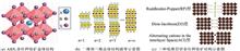
The structure of organic⁃inorganic hybrid perovskites and their corresponding solar cells were overviewed. The characteristics of ionic liquids and applications of ionic liquids in three-dimensional hybrid perovskite solar cells were summarized.And then the effects of different ionic liquids on the properties of low-dimensional layered perovskite films and devices were introduced,the applications of ionic liquids as organic spacer in low-dimensional layered hybrid perovskite solar cells were emphasized. Finally, the problems existing in the applications of ionic liquids were discussed, as well as the future research directions in this field.
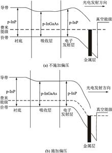
The development of field-assisted photocathode was reviewed, and the working principle of field-assisted photocathode was introduced. Three representative cathode structures were summarized systematically, which were InP/InGaAsP/InP, InP/InGaAs and InGaAs/InAsP/InP photocathode. InP/InGaAsP/InP double heterojunction was a research highlight in field-assisted photocathode research, and this structure was mostly used in 1.3 μm field-assisted photocathode; InGaAs heterojunction structure had high sensitivity and fast response time compared with other structures, which was conducive to the application of fringe image converter tube; the photocathode with InGaAs/InAsP/InP structure provided a graded InAsP layer between InP and InGaAs, which was very beneficial to prolong the wavelength threshold. By analyzing the characteristics and applications of different structures, the development direction and difficulties of field-assisted photocathodes were discussed.
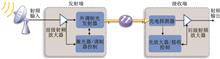
Microwave photonic Transmitter/Receiver are core components for electro-optic (EO) / opto-electric (OE) conversions in the microwave photonic systems, and have been widely used in radar, electronic warfare, communication and etc. In this paper, the principle and typical products of microwave photonic Transmitter/Receiver (T/R) were introduced, and the development trend and key technologies were discussed.
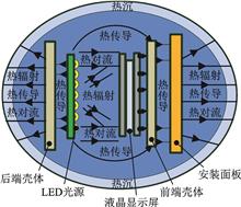
The cooling methods of structural parts and thermally conductive materials were analyzed, and meanwhile the heat dissipation design of the display was carried out by using the LED light source assembly to dissipate heat and increase the heat dissipation area. It ensured that the display could operate normally with high brightness in high temperature environment. Combined with thermal simulation, experiments showed that the proposed display heat dissipation design could meet the reliability requirements.
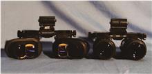
A novel measurement method of field of view (FOV) was proposed based on high precision turntable, which was consistent with the designed value of FOV. The novel method could solve problems, such as adjustment difficulty, large error and long time consuming in traditional measurement methods of FOV and image continuity, thus providing reference for the measurement and improvement of PNVG.
The technical approaches and reliability of the active optoelectronic devices were studied, including coaxial and box-type package structure, electrical and optical parts attachment materials and fiber coupling system.The characteristics of attachment material for electrical parts and cementing material for optical parts were compared and analyzed. The structural characteristics of direct and indirect coupling in fiber coupling system were described,as well as the optical window sealing technologies in indirect coupling,three sealing methods and reliability of fiber and pigtail ferrule in direct coupling.In addition, several reliability verification methods were presented, aiming at the typical failure modes of active optoelectronic devices.
The development process of the digital low⁃light level (LLL) night vision technology was reviewed, and the detection mechanism and imaging characteristics of some mainstream LLL detection products based on digital image processing technology were expounded. The advantages and disadvantages of various detectors in different applications were introduced and compared. At the same time, the future development direction and application prospects of digital LLL detection technology were analyzed.
Characteristics and typical applications of micromation LED display technologies were introduced, with analysis of the key technologies and solutions related to micromation LED display. Domestic and international research progress of micromation LED display on technical grounds, as well as prospects were summarized. Especially in military fields, it was supposed to aiming at achieving practicality and reliability of Micro‑LED display, making emphasis on circuit control technology development, heat dissipation capability optimization, and special technical problem solutions, such as NVIS and EMC.
The opportunities and challenges of developing OLED defect inspection technology and equipment for CELL segment were analyzed, and the OLED detection technologies, testing equipment and the popular equipment manufacturers for CELL segment were listed. Core products and technologies were classified and introduced. From the research point of view, the research contents of CELL segment were also classified and summarized, such as bright spot inspection, dark spot inspection and MURA detection, and the advantages and disadvantages of different methods were analyzed. Finally, the possible trends of CELL segment OLED inspection technology and equipment in the next few years were presented and discussed.
The research progress of photoelectric molecules materials was summarized, such as photochromic molecules, aggregation-induced luminescence (AIE) molecules and solar molecules from the perspective of single-molecule electrical conductivity. Next, molecular devices designed based on the electrical properties of photoelectric molecules were systematically introduced, and the advantages and shortcomings of photoelectric molecules for molecular devices were also discussed. Then the charge transport mechanism of photoelectric molecules was explored, which could provide an effective basis for further elucidating the conformational relationship between the structure and properties of photoelectric molecules. Moreover, it would provide an effective basis for the design of optoelectronic functional molecular devices at the single molecule level.
The research progress of a-IGZO was reviewed , as well as the high stability mechanism, preparation process, the element ratio between two layers, adulteration method and process parameters. In addition, the effect of dual-active layer on TFT's properties and the improved methods were comprehensively and thoroughly analyzed. Then, the future direction of a-IGZO technology was prospected.