


Please enter the answer below before you can view the full text.


2025
Volume: 54 Issue 5
16 Article(s)

Min ZHOU, Hong ZHOU, Jincheng ZHANG, and Yue HAO
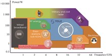
Ultra-wide bandgap semiconductor material gallium oxide (β-Ga2O3) has the properties of high critical breakdown field strength, high electron saturation velocity, and large-size single crystal substrate grown by the melt method. It is expected to find wide applications in high-voltage and high-power fields such as future power grid, rail transit, and radar communication. Although electronic devices based on gallium oxide materials have achieved rapid development in the world, the research of gallium oxide-based radio frequency (RF) devices has been restricted by low carrier mobility and poor thermal conductivity of β-Ga2O3 materials. Firstly, this paper analyzes the development needs of high-voltage RF power devices, including higher power levels, smaller and lighter equipment, and more efficient systems. Then, the reasons why gallium oxide material is suitable for future high-voltage and high-power radio frequency devices are elaborated from four aspects: breakdown field strength, saturation velocity, wafer fabrication, and thermal management. Next, the relevant research progress on gallium oxide-based RF power devices is discussed, focusing on three types of device structures: metal-oxide-semiconductor field-effect transistors (MOSFETs) on homogeneous and heterogeneous substrates, and heterojunction field-effect transistors (HFETs). Finally, it is summarized that the two major obstacles to enhancing the performance of gallium oxide RF power devices are poor thermal conductivity and low current density. In addition, the research suggestions for future work in this field are also presented, such as heterogeneous integration with high-thermal-conductivity substrates, research on surface passivation techniques, and the reliability of devices in extreme environments, providing references for researchers in related fields.
May. 20, 2025Vol. 54 Issue 5 721 (2025)
Qingbo DU, Yapeng YANG, Xudong GAO, Zhi ZHANG, Xiaoyu ZHAO, Huiqi WANG, Yier LIU, and Guoqiang LI
Silicon carbide(SiC) semiconductor material has many outstanding advantages such as wide band gap, large crystal atom departure threshold energy and high electron hole migration rate. The SiC based nuclear radiation detector has the advantages of high temperature resistance, high radiation resistance, small size and fast response. The continuous improvements of high quality, large size SiC crystal materials growth, epitaxial growth technology and device preparation technologis have greatly promoted the development of SiC based nuclear radiation detectors. This paper starts with the principle and performance evaluation index of SiC nuclear radiation detector, analyzes the interaction mode and main performance index of SiC material with various radiation particles during radiation detection, and the relationship between main performance index and SiC crystal defects, etc. Based on the physical properties of SiC crystal, the preparation and epitaxial growth methods of SiC crystal substrate at the detector level are summarized and compared. The latest research progress of SiC charged particle detector, neutron detector and X/γ detector are introduced, and the challenges in the development of SiC based nuclear radiation detector are analyzed, which provide a reference for improving the performance of SiC based nuclear radiation detector.
May. 20, 2025Vol. 54 Issue 5 737 (2025)
Jiahe LI, Lili ZHENG, Hui ZHANG, Xiang LI, and Junfeng CHEN
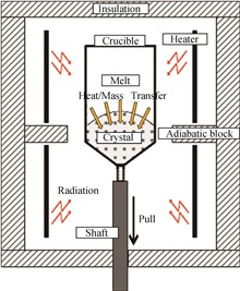
The inclusion defect in fluoride crystals significantly affects optical quality, and the formation of such defect is mainly determined by the shape of crystal interface and growth rate when using Bridgman method. This article focuses on the technique of Bridgman method, and intends to study the influence of thermal field on crystal growth rate and interface shape through numerical simulations, in an attempt to understand the underlying physics that enable the formation of a slightly convex interface shape and prolonging stable growth stage as well as to achive an effective inclusion defect control strategy. Numerical results show that the formation of interfaces with high convexity during fluoride crystal growth is mainly due to the radial heat absorption near the interface caused by internal radiation heat transfer characteristics. Increasing the length of the adiabatic block can reduce the growth rate in the initial stage and effectively reduce the interface convexity during the stable growth. Raising the temperature of the upper and lower heaters can shorten the initial unstable growth zone and effectively reduce the interface convexity during the stable growth. For the growth of large-sized or multi-crucible crystals, there exists a large radial temperature gradient, this means that the crystal growth interface is too convex. By increasing the temperature at the bottom of upper heater and adding heat dissipation openings in the adiabatic block, it is possible to establish a slightly convex interface shape which is unfavorable to inclusion defect formation.
May. 20, 2025Vol. 54 Issue 5 772 (2025)
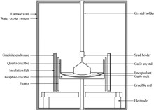
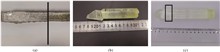
Wenwen YANG, Wei LU, Hui XIE, Gang LIU, Xinyu LYU, Yihan BAI, Chenhui LI, Jiaoqing PAN, Youwen ZHAO, and Guiying SHEN
Gallium antimonide has been widely recognized for its superior physical properties and significant application value. The first domestic 6-inch n-type Te-doped GaSb single crystal ingot was successfully grown by the research team using the liquid encapsulated Czochralski method. High-quality 6-inch GaSb wafers are prepared, and the crystal quality and wafer surface properties are studied. The full width at half maximum of the rocking curve for the (400) plane of the GaSb substrate is only 20″, and the average dislocation density is approximately 3 177 cm?2. The surface roughness (Rq) is 0.42 nm, and the oxide layer thickness is 2.92 nm. These results demonstrate the high crystalline quality and excellent surface morphology of the 6-inch GaSb single crystal. In addition, numerical simulations of the growth process of the 6-inch GaSb single crystal are conducted, revealing the thermal field distribution, flow field distribution, and solid-liquid interface deflection. These findings provide new insights for the high-quality growth of GaSb materials and lay a foundation for the industrial application of large-sized crystals.
May. 20, 2025Vol. 54 Issue 5 784 (2025)
Wenyu LIU, Lu QIAN, Fangjian LI, Shangke PAN, Zhigang SUN, Hongbing CHEN, and Jianguo PAN
In the research on cryogenic radiation detectors for neutrinoless double β decay, the growth and luminescence properties of Li2MoO4 crystals were studied. Commercially sourced Li2MoO4 powder was used as the starting material and was purified through the horizontal zone melting method. A 1 inch (1 inch=2.54 cm) transparent Li2MoO4 crystal was grown by Bridgman method. Phase analysis and luminescence property characterization were conducted on the crystal. X-ray powder diffraction reveals that the crystal belongs to the hexagonal system, with a space group of R3 and unit cell parameters a = 14.337 ?, b = 14.337 ?, and c = 9.589 ?. Inductively coupled plasma mass spectrometry shows that the contents of impurity elements Rb, Cs, Cu, Cr, Mn, Ni, Th and U in the crystals grown after purification were significantly reduced. Differential thermal analysis shows that its melting point is 696 ℃. The maximum optical transmittance, measured by ultraviolet-visible spectrophotometry, was found to reach 86%, indicating that the crystal has high optical quality and low impurity content. Steady-state and transient fluorescence spectra were measured, showing that the temperature-dependent fluorescence spectra and photoluminescence decay time of the Li2MoO4 crystal varied within the temperature range from 10 K to 300 K. It was observed that fluorescence intensity peaked at 10 K, while the photoluminescence decay time reduces with rising temperature, reaching 1 222.6 μs at 10 K. The activation energy Ea of the crystal is 6.15 meV. These findings suggest that the Li2MoO4 crystals grown by this method exhibit excellent luminescence properties at low temperatures, making them highly suitable for application in neutrinoless double β decay research, particularly in cryogenic radiation detectors.
May. 20, 2025Vol. 54 Issue 5 793 (2025)
Runlong SHANG, Ya CHEN, Yang RUI, Liguang WANG, Cheng MA, Ran YI, and Shaolin YANG
Insulated gate bipolar transistor (IGBT) is a core device for energy conversion and transmission, which widely used in rail transportation, smart grid, aerospace, electric vehicles and other fields. As the substrate material for IGBT chips, the quality of lightly phosphorus-doped silicon wafers with ultra-low oxygen content plays a crucial role in the performance of IGBT chips. Due to the use of oxygen-containing quartz crucibles during the Czochralski (CZ) method for monocrystalline silicon growth, the oxygen content of the obtained silicon is typically 4×10¹⁷~9×10¹⁷ atoms/cm3, which is much higher than the oxygen content of less than 2.5×10¹⁷ atoms/cm3 required for IGBT silicon wafers. To solve the above problems, this article presents a numerical simulation of monocrystalline silicon growth using a 32 inch hot zone, and designs a new heater to produce ultra-low oxygen monocrystalline silicon ingots that meet the requirements of IGBT substrates. The simulation results show that the flow rate of silicon melt near the quartz crucible wall and solid-liquid interface decreases when using a split heater. This phenomenon is beneficial to reduce the oxygen content in the melt and the transport of oxygen impurities to the solid-liquid interface, thereby effectively reducing the overall oxygen content of the crystal rod. In addition, due to the use of a split heater, the axial temperature gradient of the crystal rod at solid-liquid interface is significantly reduced compared to conventional heaters, which is also beneficial to reduce the oxygen content in the silicon rod. The experimental results further confirmed the simulation results. The oxygen content of the monocrystalline silicon rod produced under the split heater is much lower and remains below 2.5×10¹⁷ atoms/cm3 throughout, fully meeting the requirements for IGBT substrates.
May. 20, 2025Vol. 54 Issue 5 801 (2025)
Xiuyang JIA, Zhigang JIA, Hailiang DONG, Xiaodong CHEN, Maolin GAO, and Bingshe XU
The 795 nm vertical-cavity surface-emitting laser (VCSEL), commonly used as a laser source in rubidium atomic clocks and quantum gyroscopes, is generally designed with a single oxide confinement layer structure to ensure single-mode output. However, the output power in this structure is limited, and power consumption remains high. In this paper, PICS3D was used to simulate the position of single oxide confinement layer. The results demonstrate that as the oxide confinement layer is positioned closer to the active region, its ability to confine carriers increases. Consequently, under identical injection current conditions, devices exhibit higher output power. On this basis, symmetric double oxide confinement and quadruple oxide confinement structure VCSEL close to the active region are designed. Compared with traditional single oxide confinement VCSEL, multi oxide confinement VCSEL exhibits higher current density in the active region, the output power and power conversion efficiency are significantly improved. In addition, this paper also analyzes the effect of the number of oxide confinement layers on the optical performance of the device through the far-field and near-field, and finds that with the increase of the number of oxide confinement layers, the higher-order modes of the VCSEL are more concentrated in the exit aperture and the far-field divergence angle increases. This study is of great significance for optimizing the VCSEL performance using multiple oxide confinement and balancing the output power and optical performance.
May. 20, 2025Vol. 54 Issue 5 809 (2025)
Jiayi ZHU, Shuai DU, Pengfei ZHOU, Fan ZHENG, and Yunlin CHEN
LiNbO3/ITO(LN/ITO) heterojunction thin films were sputter-deposited on glass and silicon substrates using magnetron sputtering technique at 200 ℃. The structure, morphology, and optoelectronic properties of the films were characterized through X-ray diffraction (XRD), atomic force microscope (AFM), ultraviolet-visible spectrophotometer, and variable temperature Hall effect measurements. XRD analysis reveals that the stacked sequence of LN/ITO heterojunction exhibited superior growth orientation and crystalline properties. AFM images show that the surface of the heterojunction thin film at 200 ℃ is relatively smooth with minimal protrusions. The ultraviolet-visible spectrophotometer indicates that the transmittance of the stacked heterojunction thin film in the visible light range was enhanced compared to that of the LN single-layer film, and the transmittance of the heterojunction film was further improved after annealing. The electrical properties of the LN/ITO heterojunction were investigated using a Hall effect tester. The results demonstrate that the LN/ITO heterojunction thin film is an p-type semiconductor. Compared to the LN single-layer film, the conductivity of the LN/ITO heterojunction thin film was increased by 11 orders of magnitude.
May. 20, 2025Vol. 54 Issue 5 819 (2025)
You XIE, Xiaosa XIAO, Ningning JIANG, and Tao ZHANG
The two-dimensional heterostructures have outstanding physical and chemical properties that make them promising applications in nanoelectronic devices. A novel BC6N/BN lateral heterostructure was constructed, and the structural stability, electronic structure, conductivity and volt-ampere characteristics of BC6N/BN lateral heterostructure were investigated by the first-principles combined with the non-equilibrium Green's function. The BC6N/BN lateral heterostructure not only exhibits dynamic stability but also possesses a direct bandgap of 2.01 eV, static potential difference generated at heterojunction interface, electrons and holes form an electrical barrier at the interface. Compared to the BC6N and BN monolayers, the conductivity of BC6N/BN lateral heterostructure is significantly reduced and exhibits strong anisotropy. The volt-ampere characteristics of the BC6N/BN lateral heterostructure show that almost no current is generated in the voltage range of 0 to 2.5 V. After the forward voltage exceeds 3 V, the current shows a linear increase trend; during the process of increasing the reverse voltage from 3 V to 5.5 V, there is only a weak current. When the reverse voltage exceeds 5.5 V, the current increases nonlinearly. Therefore, the BC6N/BN lateral heterostructure has anisotropic conductivity and unidirectional conductivity characteristics, which can provide the important theoretical basis for the design and preparation of nanoelectronics devices.
May. 20, 2025Vol. 54 Issue 5 825 (2025)
Yuhua WEI, Xinhua CHEN, Shuai JIANG, Xiaoshuang LI, and Jianguang WANG
Multi-stable metamaterial can deform under external forces, enabling flexible manipulation of elastic wave propagation. This paper proposed two multi-stable metamaterials based on the bistable flexural elastic beam structure, with different bending dimensions. These metamaterials possess two stable configurations and can switch between these states under the external forces. The dispersion relation and frequency response characteristics of the multi-stable metamaterial in the two stable configurations were investigated by the finite element method. The results reveal that by adjusting the external applied forces, the stable structure can be deformed, effectively tuning the frequency range and bandwidth of the bandgap. A wider first bandgap range can be obtained by expanding one-dimensional multi-stable metamaterial into three-dimensional multi-stable metamaterial. This shape-changing mechanism not only provides diverse control methods for elastic wave propagation but also offers new insights into the design and application of elastic waveguide switch.
May. 20, 2025Vol. 54 Issue 5 832 (2025)
Jian CUI, Zhihao HE, Jiafu DING, Yunjie WANG, Fuhong WAN, Jiajun LI, and Xin SU
This study is based on the first-principles method to comparatively study the electronic structure and optical properties of tungstate TMWO4 (TM=Zn, Cd, Hg). The research results show that ZnWO4, CdWO4 and HgWO4 are all direct band gap materials, and the band gap widths are 2.579, 2.081 and 2.538 eV. The top of the valence band of the three compounds is mainly contributed by the O-2p state. Due to the hybridization effect, the O-2p state and the W-5d state form the bottom of the conduction band together. Analysis of the bond population and electron localization function shows that, there are two kinds of W—O bonds, of which the W—O1 long bond is ionic bond, and the W—O2 short bond is covalent bond; the metal cations form ionic bonds with O atoms.Each type of tungstate exhibits differences in dielectric functions at different directions. A larger Δε has a positive impact on the birefringence Δn. As the radius of the metal cation with d10 electronic configuration increases, the birefringence of the crystal decreases. The birefringence of ZnWO4, CdWO4 and HgWO4 are 0.192, 0.187 and 0.078 at 1 064 nm. Among the three systems, ZnWO4 and CdWO4 show larger birefringence and anisotropy.
May. 20, 2025Vol. 54 Issue 5 841 (2025)
Longjun REN, Shihu CAI, Fuyuan WANG, and Ping JIANG
Two-dimensional materials have excellent electronic and optical properties, indicating their absolute advantage in the application of nanodevices. In this work, a novel two-dimensional material with a wrinkled structure (monolayer C2B6) was proposed, and its dynamic and thermal stability were calculated through first-principles simulations. It is interesting that monolayer C2B6 exhibits semiconductor behavior, while HSE06 calculation shows its ultra narrow bandgap of approximately 0.671 eV. The holes in monolayer C2B6 exhibit an ultra-high mobility of approximately 6 342 cm2·V-1·s-1 in the transport direction, which is greater than that of traditional transition metal disulfide materials. More importantly, the significant anisotropy of electron and hole mobility can separate photogenerated charges, indicating that monolayer C2B6 is an excellent photocatalyst. Then, new characteristics of light absorption were obtained, and anisotropic photocurrent also implies that monolayer C2B6 can be used as a potential optoelectronic device. Our research results provide theoretical guidance for the design and application of two-dimensional materials.
May. 20, 2025Vol. 54 Issue 5 850 (2025)
Zhicheng SONG, Bo ZHANG, Chunfu ZHANG, Xiaoyong QU, Yufeng NI, and Jiaqing GAO
Introducing the tunneling oxide passivated contact (TOPCon) structure into the back contact solar cells structure, a tunneling oxide passivated contact back contact (TBC) solar cell was prepared, which can effectively suppress the recombination of electrons and holes, and improve the photoelectric conversion efficiency. This article focuses on the preparation process of the emitter of p-type TBC solar cells, and deeply studies the preparation process and passivation performance of n-type tunneling oxide passivation contact structures (n-TOPCon) on p-type silicon wafers. Through experiments, the influence of oxidation time on the thickness of the oxide layer during the growth process of the tunneling oxide layer was studied, and the effect of different thicknesses of tunneling oxide layers on the passivation of the emitter n-TOPCon structure was investigated. The experimental results show that at an oxidation temperature of 600 ℃ and an oxidation time of 1 200 s, the tunneling oxide layer thickness reaches 1.52 nm, and the optimal passivation performance could be obtained. At this time, the hidden implied open circuit voltage reaches 733 mV, corresponding to J0 of 4.41 fA/cm2. Afterwards, the doping distribution curve and passivation performance of n-TOPCon emitter under different phosphorus diffusion temperatures and phosphorus source flow rates were studied. When the diffusion temperature reaches 870 ℃, the implied open circuit voltage of n-TOPCon can be increased to 736 mV. As the diffusion temperature increases, the implied open circuit voltage of the emitter n-TOPCon structure begins to decrease. Finally, the relationship between the passivation performance of n-TOPCon structure and N2-POCl3 flow rate was studied under the same diffusion temperature. Through experiments, it is found that with the increase of diffusion N2-POCl3 flow rate, the passivation performance of n-TOPCon structure first improve and then decrease. According to the test results, when the N2-POCl3 flow rate is 3 000 sccm, the hidden open circuit voltage of n-TOPCon structure can be increased to 740 mV.
May. 20, 2025Vol. 54 Issue 5 857 (2025)
Zhichao WANG, Linfeng YE, Miao RUAN, Chao YANG, Xuefeng JIA, Yufeng NI, Yonggang GUO, and Peng GAO
To passivate defects in perovskite and enhance perovskite flims quality,a novel small molecule,2-amidinoethylenediamine dihydrobromide (2AD), was designed for interfacial modification of mixed-cation mixed-halide perovskite ((FA0.90MA0.05Cs0.05) Pb(I0.96Br0.04)3) flims with a bandgap of 1.55 eV. The inverted perovskite solar cells (PSCs) were fabricated via an anti-solvent method using chlorobenzene, followed by systematic analysis of phase composition, optoelectronic properties, and device performance. Experimental results demonstrate the multifunctional effectiveness of 2AD in three key aspects: 1) the grain size of perovskite films increases from 304 nm to 321 nm, accompanied by reduces surface roughness from 16.6 nm to 15.8 nm, and enhances hydrophobicity contact angle from 70.1° to 74.3°,the hydrophobicity increases; 2) the photogenerated carrier lifetime is significantly prolonged, effectively suppressing non-radiative recombination and facilitating charge transfer; 3) unencapsulated devices retains over 90% of their initial power conversion efficiency after 30 d exposure to ambient atmosphere. Finally, the efficiency of the perovskite device increases from 21.32% to 23.49%, and the hysteresis factor significantly reduces.
May. 20, 2025Vol. 54 Issue 5 873 (2025)
Qi SONG, Ling JIANG, Hongming CHEN, Huifu LI, Shuo HUANG, Lijie LUO, and Yongjun CHEN
Zinc-ion capacitors are one of the promising options for emerging electrochemical energy storage devices. Nevertheless, the thermodynamic interactions between zinc metal and aqueous electrolyte lead to corrosion and uncontrolled growth of zinc dendrites, which significantly compromise the Coulombic efficiency and the cycle lifespan of zinc-ion capacitors. To mitigate the adverse side effects associated with the zinc anode in aqueous environments, this study presents the development of a kapok fiber porous carbon material (KFC) featuring sub-nano-channels, synthesized through a one-step carbonization process utilizing kapok fiber biomass. Subsequently, zinc anode coated with KFC layer, resulting in the formation of a Zn@KFC composite anode. The sub-nano-channels within the KFC facilitate the continuous adsorption of water molecules from the solvented zinc-ions, thereby promoting a gradual desolvation process that enhances the rapid and uniform transport of zinc-ions. This mechanism effectively reduces water-induced corrosion of the zinc anode and minimizes side effects. The experimental results indicate that the Zn@KFC symmetric cell demonstrates an impressive cycle life exceeding 1 000 h at 1 mA·cm-2 and 1 mAh·cm-2. Even under harsh conditions of 5 mA·cm-2 and 5 mAh·cm-2, its cycle life can still exceed 400 h. Additionally, the zinc-ion capacitor utilizing the Zn@KFC anode electrode exhibits exceeding 50 000 cycles, with a Coulombic efficiency approaching 100% (capacity retention rate of 98.29%). This approach to enhancing the reversibility of zinc anode through surface modification offers a novel strategy for the development of high-performance zinc-ion capacitors.
May. 20, 2025Vol. 54 Issue 5 882 (2025)
Feng YU, Qiang ZHENG, Tingyu QI, Yubai ZHANG, Yali MA, Songyan JIA, and Xue LI
Aragonite calcium carbonate whiskers with a high aspect ratio were prepared by carbonization method using high concentration dolomite refined solution as the raw material. The calcium carbonate whisker samples were characterized by XRD, SEM, TEM, etc. The effects of carbonization temperature, stirring rate, CO2 aeration rate, and aging time on the dispersion degree and aspect ratio of calcium carbonate whiskers were investigated. The results show that the optimum process conditions for the preparing calcium carbonate whiskers are as follows: carbonization temperature 80 ℃, CO2 aeration rate 25 mL/min, stirring rate 200 r/min, and aging time 1 h. Under these conditions, calcium carbonate with a yield of 95%, whisker aspect ratio of 30~35, whisker content of 99.7%, whiteness of 99.9%, and uniform distribution can be obtained. The growth mechanism of calcium carbonate was analyzed. The results show that Mg2+ can inhibit the growth of calcite calcium carbonate and promote the growth of aragonite calcium carbonate during the carbonization process, and calcium carbonate whiskers have a preferential growth along (120) crystal plane.
May. 20, 2025Vol. 54 Issue 5 898 (2025)
© Copyright 2018-2021 | Chinese Laser Press.
All Rights Reserved 沪ICP备15018463号-20