


Please enter the answer below before you can view the full text.


2025
Volume: 52 Issue 1
31 Article(s)

Jinchun Liu, Shurong Luo, and Feng Huang
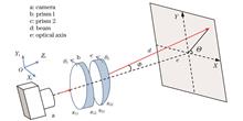
ObjectiveTarget-tracking control technology is extensively employed in several fields, including aerospace, satellite remote sensing, and laser communication. The Risley-prism system enables the direction of the beam to be altered or the visual axis to be adjusted by controlling the rotation angle of the prism. Compared with alternative mechanical beam-pointing mechanisms, such as gimbal and fast steering mirror mechanisms, the target tracking control system based on Risley-prisms exhibits several advantageous characteristics. These features include a compact structure, high reliability, and high pointing accuracy, which collectively provide the system with a wide range of potential applications. In the case of a traditional beam-pointing mechanism, the relationship between the pose adjustment of the actuator and target motion trajectory is characterized by intuitive linearity. However, there is a nonlinear relationship and strong coupling between the prism rotation angle and visual axis orientation of the Risley prism system, which makes it challenging to accurately determine the prism rotation angle via analytical means. Furthermore, conventional numerical methods have limitations in terms of accuracy and efficiency, which impede the advancement of research and practical applications of the Risley-prism system in target-tracking scenarios. In this study, we report a target-tracking method based on the Risley-prism system using a virtual system, whereby the spatial direction of the outgoing beam of the actual Risley-prism system is mapped. Our basic approach and discoveries provide useful insights into the design of pointing and tracking control systems based on Risley-prisms for time-varying optical targets.MethodsA particle swarm-optimized target tracking method based on a virtual system was employed in this study. First, based on the nonparaxial ray-tracing method, a virtual Risley-prism system was constructed to map the spatial direction of the outgoing beam of the actual Risley-prism system. Subsequently, by combining the virtual system model projected by the actual two-prism system with the particle swarm algorithm, multiple possible prism rotation angles (particles) and their corresponding virtual pointing targets were calculated in parallel. Subsequently, if the estimation error between the outgoing beam-pointing of the virtual Risley-prism system and the target to be tracked was less than the actual error, then the actual prism rotation angle was replaced by the estimated prism rotation angle and applied to the actual Risley-prism system. In the next step, the prism rotation angle that best matches the target to be pointed at and tracked was selected based on the interoperability and information-sharing mechanism of the particle swarm algorithm. In addition, the prism angles of the experimental prototype Risley-prism system were adjusted to realize dynamic target tracking.Results and DiscussionsThe prepared Risley-prism system based on the virtual system with the RPSO algorithm presents comparable performance for static target pointing in numerous simulations, and the final convergence accuracy of the proposed RPSO-based Risley-prism system approaches 5?10 mm (Fig. 6). In addition, when tracking a moving target, the RPSO-based Risley-prism system can converge to the global optimum more quickly than can the PSO-based method, exhibiting a faster convergence speed and higher convergence accuracy (Fig. 8). The results of the simulation analysis show the effect of particle population size on virtual system-based target tracking methods: larger particle populations lead to faster convergence but increased computation (Fig. 9). In the simulation of continuously tracking target points, the estimation error of the virtual system and real error of the Risley-prism system can still converge, indicating that the proposed algorithm still has a stable tracking effect when tracking continuously changing dynamic targets (Fig. 10). The pixel deviation distribution of the 60 target pointing tests demonstrates the excellent performance of the proposed method: the mean pointing error and standard deviation are 9.43 and 10.14 pixel, respectively (Fig. 13). In the static target pointing experiments, the proposed method demonstrates better pointing performance. The fitted circle radius of the pointing error distribution of the proposed method is smaller than that of the two-step method, and the average pointing error, root mean square error, and maximum pointing error of the proposed method are all smaller than those of the two-step method. During the dynamic tracking experiments, the Risley-prism system sequentially achieved the tracking of three targets with a final pixel error of approximately 13.04 pixel, thus demonstrating the excellent performance of the proposed target-tracking method in the application of continuous target tracking. The performance difference in dynamic target pointing tracking shows that the performance of the proposed RPSO-based algorithm is superior to that of the two-step method. The average tracking errors (in pixel) and the root-mean-square (RMS) tracking errors of the two algorithms are as follows: 10.64 pixel and 11.22 pixel (two-step method) and 8.113 pixel and 9.429 pixel (proposed method), respectively.ConclusionsThis study successfully develops a new Risley-prism system-based target tracking method by introducing a combination of particle swarm optimization and a virtual system into an actual Risley-prism system. The particle swarm method is used to adjust the Risley prism angle and achieve target tracking in the Risley-prism system. To maintain a certain degree of correlation between the virtual and actual systems, a virtual target is constructed based on the deviation of the center of the camera field-of-view from the center of the actual target to be tracked in the x- and y-directions. The error feedback information used to estimate the prism angle in the virtual system is consistent with the tracking error fed back from the actual system, and the prism angle is calculated based on the dynamic changes of the target to be tracked. The simulation and experimental results demonstrate the feasibility of the method for achieving target tracking. In the static target experiments, the average pointing error and standard deviation are 9.43 pixel and 10.14 pixel, respectively, whereas in the dynamic target tracking experiments, the average tracking error is approximately 16 pixel at the three key positions. The proposed method provides a promising method for realizing the target pointing and dynamic target tracking of rotating Risley-prism systems with a wide range of applications.
Jan. 20, 2025Vol. 52 Issue 1 0105001 (2025)
Yajie Zheng, Qi Bian, Chen Wang, Fei Yang, Huan Wang, and Yong Bo
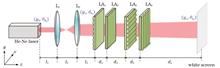
ObjectiveHigh-power lasers are widely used in various fields for industrial, scientific, and military applications. Generally, the intensity distribution of a laser beam is not uniform and generally exhibits a Gaussian distribution, which may lead to material damage during laser processing owing to the uneven energy distribution. Different application fields have different demands for the spot shape and intensity distribution of laser beams. Recently, flat-topped laser beams with a uniform distribution of beam intensity have become commonly used, with a wide range of applications in material processing, semiconductor substrate annealing, optical holography, and laser lighting. A flat-topped beam can be obtained using beam shaping technology, and common beam homogenization technologies include the light field mapping method and beam integration method. Light field mapping is realized using an aspheric lens group, a birefringent lens group, and diffractive optical elements, which are suitable for single-mode laser light sources. Beam integration is mainly performed using mirror arrays, prism arrays, and microlens arrays, which are particularly suitable for excimer lasers, multi-mode lasers, or laser light sources with irregular light intensity distribution. The microlens array homogenization system is generally wavelength insensitive, and the output spot shape is modulated by the sub-lenses. It is widely used owing to its simple structure, high damage threshold, and low transmission loss.MethodsBased on the superior properties of microlens arrays, a beam homogenization and shaping system based on cylindrical microlens arrays was designed. The microlens arrays were placed orthogonally to homogenize and shape the vertical and horizontal directions of a Gaussian circular beam, respectively, achieving a square beam output with a near-flat-top intensity distribution. Based on the theories of matrix optics and Fourier optics, the light transmission mode was analyzed, the structural parameters of the microlens array were optimized using Zemax software, and a simulation model was constructed to shape the homogenization effect of the system. The research system was established using an experimental platform. First, one pair or two pairs of orthogonal microlenses were employed to compare the Gaussian beam homogenization. With two pairs of cylindrical microlens arrays, the effect of the incident Gaussian beam diameter on the uniformity and size of the homogenized light spot was investigated experimentally and theoretically. When the input laser beam had a diameter of 8 mm, the relationship between the output spot shape and the interval distance of the microlens arrays was analyzed. Moreover, the effect of laser beam quality on homogenization and shaping was examined for the cylindrical microlens array system.Results and DiscussionsBased on the simulation result of Zemax software, the structural parameters of the microlens array are optimally designed with a sub-lens aperture size of 500 μm and a focal length of 5.4 mm. Compared with the use of one pair of cylindrical microlens arrays to homogenize and shape the horizontal and vertical directions, the experimental and theoretical results show that the Gaussian circular beam can be better homogenized with a more uniform energy distribution by utilizing two pairs of cylindrical microlens arrays placed orthogonally. As the size of the incident Gaussian beam increases, the uniformity of the homogenized spot increases and the sharpness of the spot edges decreases (Figs. 2 and 3). By controlling the interval distance between the microlens arrays, square beams with adjustable spot shapes and sizes and a near-flat-top distribution of light intensity can be obtained. With an incident spot diameter of 8 mm, homogenized output spots with adjustable beam aspect ratios such as 100 mm×100 mm squares, 100 mm×130 mm rectangles, and 130 mm×130 mm squares were successfully obtained (Fig. 4). In our case, the size of the spots increases with the transmission distance of the homogenized beams; however, the corresponding uniformity shows little change. The homogenization shaping system is flexible and versatile on a spatial scale, and it can better meet practical applications in scientific research and production. The microlens array system is insensitive to the beam quality of the incident laser, which makes it especially suitable for homogenizing and shaping excimer lasers, laser diode arrays, multimode light fields, or laser sources with irregular intensity distributions.ConclusionsIn this study, the physical mechanism and homogenization process of a cylindrical microlens array homogenization system are investigated in depth using a combination of theory and experiments. A discrete structure with two pairs of orthogonally placed cylindrical microlens arrays is designed for beam homogenization and shaping of a circular Gaussian beam in both the horizontal and vertical directions. By controlling the distance between the microlens arrays, a homogenized beam with an adjustable shape and size is obtained, and spot uniformity is maintained. These results open a novel way to realize a uniform square spot with an adjustable spot size and high flexibility in space utilization, which is suitable for practical applications in scientific research and industrial fields.
Jan. 20, 2025Vol. 52 Issue 1 0105002 (2025)
Yu Fan, Weijia Bao, Changrui Liao, and Yiping Wang
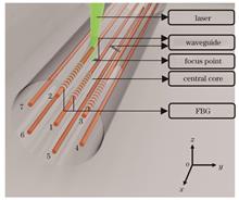
ObjectiveIn recent years, multicore fiber Bragg grating (FBG) vector displacement sensors have become a research hotspot in the field of vector displacement sensing because of their multidimensional measurement capability, high sensitivity, high resolution, and high precision. However, in practical applications, multicore FBG vector displacement sensors require a fan-in and fan-out device to realize multichannel signal demodulation. The use of this device not only increases the difficulty of fiber fusion splicing and reduces the compactibility of the sensor but also increases the cost and complexity of the system and reduces modulation efficiency, which poses a challenge to the practical application of the existing multicore FBG vector displacement sensor. In this study, a vector displacement sensing structure based on multicore FBGs and coupled waveguides is proposed, to measure multiple signals in a single channel and avoid the use of fan-in and fan-out device.MethodsFirst, for preparation, a sensing structure was studied. FBGs were inscribed in the central core (core 1) and two outer cores (core 2 and core 3) with an azimuth difference of 60° for a seven-core fiber, using femtosecond laser direct-writing technology. In addition, straight coupled waveguides for connecting core 1 to core 3 and core 1 to core 2 were prepared, to enable signal light transmission back and forth between the central and outer cores. Figure 2 shows the principle of multiplexing multichannel sensing signals, using a single core based on this structure. Subsequently, the principle of displacement sensing based on multicore FBGs was theoretically analyzed. Finally, based on the self-built displacement testing system (Fig. 7), a displacement-sensing test was performed on the prepared sensing structure, to verify its performance.Results and DiscussionsFemtosecond laser direct writing technology was used to prepare a reference FBG (FBG1) for auxiliary positioning and temperature compensation in core 1, and a sensing FBG (FBG2 and FBG3) for detecting displacement changes in core 2 and core 3. The lengths of FBG1‒FBG3 were 5 mm. Subsequently, two coupled waveguides for connecting core 1 & core 2 (waveguide 2) and core 1 & core 3 (waveguide 3) were prepared using line-by-line technology. Waveguide 2 was located upstream of the fiber with a width of 5 μm, whereas waveguide 3 was located downstream with a width of 7.5 μm. The reason for the different widths of the two waveguides was to make the reflection intensities of FBG2 and FBG3 closer to facilitate demodulation. Finally, the reflection spectra of FBG1‒FBG3 measured by a single-mode fiber circulator (Fig. 5) show that the reflection intensity of the three FBGs were basically close to being the same. The end-side light distribution (Fig. 6) shows that the prepared coupled waveguides exhibit good light-conduction performance. Subsequently, a displacement sensing test was performed based on the displacement testing system (Fig. 7). First, the directional response of the sensing structure in the direction angle of 0‒360° was tested in 10° increments, verifying that the directional response of this sensing structure approximately follows a sinusoidal distribution [Fig. 8(a)]. The phase difference between FBG2 and FBG3 was 60°, which is consistent with the theoretical analysis results. In addition, the displacement response under the most sensitive direction angle was tested, verifying a maximum displacement sensitivity of approximately 0.28 nm/mm. Subsequently, the directional response was reconstructed to verify the accuracy of the sensing structure in detecting the displacement direction. After three repeated measurements (0‒360°, in increments of 20°), the corresponding relationship between the applied angle and average calculated reconstructed angle was obtained [Fig. 9(a)]. From the linear fitting of the reconstruction angle, the actual applied direction was observed to be in good agreement with the calculated reconstruction result. Moreover, the average reconstruction errors of each angle in three repeated experiments were measured, and the overall error range was within ±5° [Fig. 9 (b)]. Finally, to investigate the performance of the sensor structure in detail, additional groups of the directional and displacement responses of FBG2 and FBG3 were tested. The directional response of FBG2 and FBG3 (0‒360°, in increments of 10°) for a displacement range of 0.5‒3.0 mm [Figs. 10 (a) and (b)] and the displacement response of FBG2 and FBG3 (0‒3 mm, with a step of 0.5 mm) in all directions (0‒360°, in increments of 40°) were tested. The results indicate that the direction and magnitude of any displacement can be determined by monitoring the wavelength shifts of FBG2 and FBG3, using displacement vector synthesis. By setting more groups of displacements and directions and averaging the FBG wavelength shift in each group, more comprehensive and accurate two-dimensional vector displacement sensing can be achieved in the fiber radial direction.ConclusionsThis study demonstrates a novel single-channel measurement multicore FBG vector-displacement sensing structure. Using femtosecond laser direct-writing FBGs and coupled waveguides in multicore fibers, the multiplexing of multichannel signals was realized in a single core. This structure avoids the use of conventional fan-in and fan-out devices, reduces the cost and complexity of multicore FBG vector-displacement sensing systems, and realizes a highly integrated sensing structure. The design and fabrication processes of FBGs and coupled waveguides are discussed. The widths of waveguide 2 and waveguide 3 were determined to be 5.0 μm and 7.5 μm, respectively. The end-side light distribution of the structure verified the satisfactory light conduction performance of the waveguide. Two-dimensional vector displacement sensing in the direction of 0‒360° was subsequently tested based on this structure, and the results of the reconstructed direction indicated the directional accuracy of this sensing structure. Finally, the direction response of the structure under different displacement sizes was tested, verifying a series of stable responses that followed an approximate sinusoidal distribution. The displacement responses at different direction angles were also tested, and the maximum displacement sensitivity of the structure was approximately 0.28 nm/mm. The experimental results show that by monitoring the wavelength shift of FBG2 and FBG3 and by further employing the method of displacement vector synthesis, such a structure can finally determine the direction and magnitude of displacement and realize two-dimensional vector displacement sensing. Such a sensing structure has good compactibility and low preparation difficulty, making it applicable to intelligent machinery, shape monitoring, crack growth monitoring, and other fields in the future.
Jan. 10, 2025Vol. 52 Issue 1 0106001 (2025)
Yanpeng Zhang, Meng Wan, Xiaoqi Zhu, Rongrong Zhang, and Bingqing Zhang
ObjectiveWith the acceleration of urbanization and increase in population mobility, the passenger volume handled by urban rail transit systems is continuously increasing. Subways are one of the primary methods by which to effectively alleviate traffic pressure in large cities. Thus, accurate train position information is crucial for ensuring the safe operation of subways. The communication-based train control (CBTC) system, which is the primary subway train operation control system, relies on train position information to ensure the safe and efficient operation of trains on the line. Existing CBTC systems employ train positioning technologies, such as axle counters, wireless local area network (WLAN), long-term evolution (LTE), and cross-induction loops. However, these positioning technologies have issues, such as a large number of trackside devices, susceptibility to electromagnetic interference, scarcity of spectrum resources, and low positioning accuracy, which limit the development of CBTC systems. In recent years, visible light communication technology has developed rapidly, exhibiting features such as concurrent lighting and communication, simple equipment, strong anti-interference capabilities, a license-free spectrum, and high positioning accuracy. Such technology is widely applied in fields such as medical care, visual signal and data transmission, and underwater communication. Therefore, there are broad prospects for applications of visible light communication in CBTC systems for subway, including high-precision train positioning.MethodsTo address the issue of high-reliability positioning for trains operating in subway tunnels, a train positioning method using visible light communication with target tracking and particle filtering is proposed. First, LED lamps installed on the tunnel walls at fixed intervals were modulated. A camera mounted on top of the head of the train captures images of the LED lamps on the tunnel walls, demodulates them to obtain the corresponding LED identity information, and then queries the line database to acquire the world coordinates of the LED lamps. Second, using Kalman filtering and the Camshift algorithm, the target was tracked and its trajectory was predicted to quickly locate the positions of the LED lamps in the imaging plane. Thus, the center coordinates of the light spot were obtained. The attitude angle information obtained from the inertial measurement unit (IMU) and conversion relationship between the coordinate systems were then utilized in combination with geometric features to calculate the world coordinates of the train's position. Next, a particle filter fusion algorithm was employed, wherein the train positioning results were used as observations and the information obtained from the speed sensor was used as the state transition equation. This fusion process combines the training positioning results with the position information from the speed sensor to optimize the positioning accuracy of the train. Finally, a visible light communication positioning experimental platform was set up, and MATLAB software was used to conduct simulation experiments on the positioning algorithm. We conducted tests on the static and dynamic positioning performance of the proposed positioning method and compared it with other positioning methods.Results and DiscussionsA train positioning experimental platform with dimensions of 20 m×1.5 m×1.0 m is established to validate the effectiveness of the proposed train positioning algorithm. Twenty test points, spaced at 0.5 m intervals, are set up at a horizontal distance of 1.5 m from the LED lamps. The experiments are conducted at speeds of 0, 40, 60, 80, 100, and 120 km/h. To reduce random errors, each test is repeated five times, and the average of the five tests is considered as the final positioning result for performance comparison and analysis. The proposed method of train positioning is compared with the methods of perspective arcs and Bayesian forecasting using visible-light imaging. The experimental results show that the maximum positioning error in the static state is 24.53 cm, and 99% of the static positioning errors are within 25 cm, indicating good overall positioning performance. Under moving conditions, the closer the receiver is to the transmitter and the slower the speed of the train, the more accurate the positioning is. At a speed of 120 km/h, the maximum positioning error is 38.25 cm, and 84% of the dynamic positioning errors are within 25 cm. Hence, the overall positioning accuracy is stable and good, demonstrating that the proposed method achieves good positioning accuracy in most cases. In comparison, the positioning accuracy of the proposed algorithm is higher, and its overall positioning stability is better than those of visible light imaging positioning methods and methods based on machine learning and visible light imaging. These results suggests that the proposed method improves the accuracy and robustness of the train positioning.ConclusionTo address the issues of insufficient positioning accuracy and the interruption of train positioning in subway tunnel environments, a visible light communication train positioning method based on target tracking and a particle filter is proposed. This method effectively reduces the number of trackside devices, provides high positioning accuracy, and possesses a strong anti-interference ability. By simulating the operating environment of subway trains, the proposed method uses LED lamps as transmitters and cameras as receivers to capture the identity information of LED lamps, and thereby convey position information. Through target prediction and tracking, this method quickly finds the position of the LED lamps in an image and obtains the center coordinates of the lamp spot, thus solving the problems of spectrum resource scarcity and susceptibility to electromagnetic interference in existing train positioning technologies. A particle filter algorithm is utilized to optimize the train positioning results, resolve the issue of positioning interruption when the number of LED lamps is insufficient during the train positioning process, and effectively improve the accuracy and robustness of positioning under train operating conditions. Hence, this method provides a new option for train positioning in CBTC systems oriented toward vehicle-to-vehicle communication.
Jan. 20, 2025Vol. 52 Issue 1 0106002 (2025)
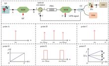
Jiacheng Bai, Bing Lu, Jiaxin Zhang, Yifan Bai, and Pengxing Guo
ObjectiveIn radar systems, single-chirped waveforms are susceptible to the range-Doppler coupling effect in high-speed moving target detection, which limits the performance of radar target tracking and detection. To overcome the influence of the range-Doppler coupling effect, a dual-chirp microwave waveform is proposed. Recently, electro-optic external modulation-based techniques have become the main schemes adopted in microwave photonic signal generation systems, as they can generate high carrier frequency and large time-bandwidth product (TBWP) dual-chirp signals; however, these schemes face problems such as system complexity (e.g., using complex devices such as dual-polarization quadrature phase shift keying modulators), implementation difficulty (e.g., requiring cutting of parabolic signals, power amplification, and other complex processing), and high cost (e.g., using swept-frequency lasers). Therefore, photonic-assisted wideband dual-chirp microwave signal generation with a large TBWP comprising a fiber Bragg grating (FBG) is proposed and demonstrated experimentally. The scheme generates a high-carrier-frequency, large-bandwidth dual-chirp microwave signal using a simple and low-cost system, and the generated signal exhibits good sidelobe suppression and pulse compression performance. Additionally, this scheme has the advantages of a wide frequency tuning range and tunable signal parameters. It is expected to provide a stable and reliable signal source for future radar systems, with a high joint range-velocity resolution.MethodsThe wideband dual-chirp microwave signal generation system based on FBG is mainly composed of a laser diode (LD), Mach?Zehnder modulator (MZM), optical circulator, FBG, optical coupler (OC), and photodetector (PD). First, a continuous optical carrier signal from the LD is sent to the first MZM biased at the maximum transmission point (MATP). Subsequently, the ±2nd-order optical sidebands and optical carriers are generated by controlling the power of the radio frequency (RF) signal. The modulated output optical signal passes through the optical circulator and then through the FBG with a 3 dB bandwidth of 17.5 GHz, which separates these ±2nd-order optical sidebands and the optical carrier. Later, the baseband single-chirp signal modulates the ±2nd order optical sidebands through the other MZM biased at the minimum transmission point (MITP). Finally, the modulated ±2nd order optical sidebands and the optical carrier reflected from the FBG are combined and sent to the PD for photoelectric conversion. After photoelectric conversion, dual-chirp microwave signals with double RF frequency and large time-bandwidth products can be generated. Dual-chirp microwave signals with tunable center frequencies are realized by tuning the frequencies of the radio-frequency signals loaded on the MZM.Results and DiscussionsTo verify the feasibility of the proposed wideband dual-chirp microwave signal generation scheme, based on the system schematic shown in Fig. 1, this study conducted an experimental validation. First, a dual-chirp microwave signal with a carrier frequency of 20 GHz, bandwidth of 1 GHz, and time-bandwidth product of 1000 is generated (Figs. 5 and 6). By matched filtering of the generated dual-chirp microwave signal, the autocorrelation function plot of the signal shows that the peak sidelobe ratio is approximately 14.7 dB. Additionally, the pulse compression ratio is approximately 893, which indicates that the generated dual-chirp microwave signal has good detection and pulse compression performance (Fig. 7). The frequency of the RF signal is varied to generate dual-chirp microwave signals with center frequencies between 16?28 GHz and a bandwidth of 1 GHz in both cases; the instantaneous frequency of the generated signal has high linearity (Fig. 8). Meanwhile, the fuzzy function and contour map of the dual- and single-chirp microwave signals have been simulated to illustrate that the dual-chirp microwave signal can solve the range-Doppler coupling effect (Fig. 9).ConclusionsThis study proposed and experimentally verified a wideband dual-chirp microwave signal generation scheme based on a narrowband FBG. The proposed scheme has the advantages of low cost, simple operation, and wide frequency tuning range. In the experiment, dual-chirp microwave signals with carrier frequencies ranging from 16?28 GHz, a bandwidth of 1 GHz, and a time-bandwidth product of 1000 were generated. Through matched filtering of the generated dual-chirp microwave signals, the autocorrelation function plot of the signals showed that the peak sidelobe ratio was approximately 14.70 dB, and the pulse compression ratio was approximately 893, which indicated good detection and pulse compression performance of the generated dual-chirp microwave signals. A radar system for detecting high-speed moving targets was constructed, and the detection performance of the generated signal was analyzed. The results showed that the generated signal could overcome the ambiguity of the joint measurement of distance and velocity that exists in a single-chirp signal. The signal could accurately obtain the velocity and position information of a high-speed moving target, further applicable to modern radar systems.
Jan. 20, 2025Vol. 52 Issue 1 0106003 (2025)
Jiakang Li, Yusheng Yao, Dongfang Jia, Chunfeng Ge, Zhaoying Wang, and Tianxin Yang
ObjectiveNyquist pulse, which is characterized by rectangular spectra and sinc-shaped time-domain waveforms, is crucial in Nyquist wavelength-division multiplexing (WDM) and Nyquist optical time-division multiplexing (OTDM), which facilitate substantial enhancements in spectral efficiency and promote super-terabit transmission. Various methodologies have been proposed for generating Nyquist pulse, including nonlinear fiber effects, cascaded modulators, and regenerative mode locking. Among these methods, modulator-based techniques are notable for their capacity to yield high-quality Nyquist pulse while remaining relatively uncomplicated and facilitating miniaturized integration. Duty cycle is one of the most important metrics of Nyquist pulse. In an OTDM system, the duty cycle determines the number of signals that can be multiplexed, whereas in an optical sampling system, it determines the sampling accuracy of the signal. However, Nyquist pulses generated by cascaded modulators have limited duty cycle. First, in most of the aforementioned methods, a high-performance rectangular tunable optical filter (TOF) must be utilized to obtain a Nyquist pulse with adjustable duty cycles, which increases the cost and complexity of the system. Second, the duty cycle of Nyquist pulse generated by cascaded modulators is limited to 0.0372. Hence, a straightforward and effective approach must be devised to generate Nyquist pulse that obviates the necessity for optical filters and offers an adjustable duty cycle.MethodsA Mach?Zehnder modulator (MZM) and an arbitrary waveform generator (AWG) were used in the current experiment. The AWG can be programmed to generate electric-frequency combs (EFCs) with different numbers of comb teeth (N), which are then used to drive the MZM to obtain a Nyquist pulse with an adjustable duty cycle. A real-time oscilloscope (Keysight, MSOV334A) with a photodiode (PD) and an optical spectrum analyzer (Yokogawa, AQ6370D) were used to observe the time-domain waveforms and spectrograms of the Nyquist pulse, respectively. However, the limited bandwidth of the oscilloscope restricts the measurement of narrower pulses. Consequently, the electrical signal frequency is reduced to 1 MHz to determine the minimum available duty cycle. Nevertheless, lower-frequency intervals cannot be measured using the optical spectrum analyzer; therefore, the homodyne method was employed to measure the spectrograms of the optical signal. This approach facilitates the detection of optical frequency combs (OFCs) with a frequency interval of only 1 MHz using an electrical spectrum analyzer (ESA), whereas the low-bandwidth real-time oscilloscope accurately measures the waveform of the Nyquist pulse.Results and DiscussionsResults show that under a fixed VPP (peak-to-peak voltage of electrical signals), the side-mode suppression ratio (SMSR) of the OFC decreases as the N of the OFC increases, and the OFC flatness deteriorates as N increases(see Fig. 4). Under a fixed N, an optimal VPP exists that optimizes the SMSR and flatness. Therefore, considering the SMSR and flatness simultaneously, an OFC with up to 121 comb teeth was generated, whose corresponding time-domain waveform was a Nyquist pulse with a duty cycle of 0.00907 (see Fig. 5). Additionally, the effect of the electrical-signal quality on the Nyquist pulse was investigated. As the maximum frequency of the EFC increases, the quality of the EFC produced by the AWG deteriorates, which primarily manifests in the deterioration of the EFC flatness (see Fig. 6). Therefore, the maximum frequency of the EFC is limited by the sampling rate of the AWG. Furthermore, the deterioration in the EFC flatness worsens the OFC flatness, with an almost identical trend exhibited (see Fig. 7). Consequently, for an AWG bandwidth of 240 MHz, the maximum EFC frequency should be limited to 70 MHz to safeguard the quality of the generated Nyquist pulses. Finally, the phase noises for the EFC and Nyquist pulse register at offsets of -97.17 dBc/Hz@10 kHz and -96.89 dBc@10 kHz, respectively, and show almost identical curves (see Fig. 8). The jitter and phase-noise measurements confirme the relative stability of the Nyquist pulse.ConclusionsHerein, we present a programmable approach for generating Nyquist pulse. Our method requires only one MZM and one AWG to produce Nyquist pulse with customizable duty cycles. Our experimental results indicate that the SMSR and OFC flatness are sensitive to both N and the electrical-signal power. Specifically, under a constant electrical-signal power, the SMSR and flatness deteriorate as N increases. Meanwhile, under a fixed N, the SMSR and flatness initially improve and then deteriorate as the electrical-signal power increases. Consequently, for each fixed N, an optimal VPPexists that optimizes the SMSR and flatness. By balancing between the SMSR and flatness, the proposed approach facilitates the generation of an OFC with up to 121 comb teeth. This corresponds to a Nyquist pulse with an exceptionally low duty cycle of 0.00907.
Jan. 20, 2025Vol. 52 Issue 1 0106004 (2025)
Bo Wang, Jianxiang Wen, Zirui Chen, Yanhua Luo, Fufei Pang, and Tingyun Wang
ObjectiveWith the rapid development of technologies such as space exploration and Starlink laser communications, active optical fibers and related devices have become widely used. Due to the unique nature of the space environment, these applications must account for the effects of radiation exposure. As a result, extensive research has been conducted to improve the radiation resistance of optical fibers. The primary focus in this field is to reduce the color center defects that arise in optical fibers after irradiation. Bismuth (Bi) is a heavy metal element with a wide range of valence states, making it particularly promising for enhancing radiation resistance in optical fibers. In this paper, we propose a cladding-doped Bi-ion erbium-doped fiber (EDF), which offers a promising solution to prevent performance degradation or failure of optical fiber devices such as optical fiber amplifiers and optical fiber lasers in irradiated environments. It has significant potential for application in radiation-affected environments.MethodsUsing GEANT4 software, the influence of varying doping concentrations of Bi ions doped in the cladding on the radiation resistance of EDFs is theoretically studied. Based on this, two types of erbium-doped fibers (EDF1 and EDF2) are fabricated using modified chemical vapor deposition (MCVD) combined with atomic layer deposition (ALD). EDF1 contains no Bi ions in its cladding, while EDF2 has Bi ions doped in the cladding. An experimental setup is used to investigate the changes in the optical fiber's spectral characteristics before and after irradiation, including radiation-induced absorption (RIA) spectra, fluorescence spectra, fluorescence lifetime spectra, gain characteristics, and laser performance.Results and DiscussionsThe simulation results indicate that doping Bi ions into the cladding of the fiber decreases energy deposition in the core, initially lowering and then increasing as the doping concentration rises, with the optimal result achieved at a doping concentration of 1.0% (Figs. 3 and 4). After irradiation with 1500 Gy, EDF2 exhibits an RIA of 5.03 dB/m at 1300 nm, which is about 37.5% lower than EDF1 (Fig. 5). The fluorescence intensity and lifetime of EDF2 declines more gradually, with smaller decreases (Fig. 6). The fluorescence lifetime decreases by 0.28 ms, representing 97.3% of the pre-irradiation value, and a 5.2 percentage points improvement compared to EDF1 (Fig. 7). The normalized radiation-induced gain variation (RIGV) of EDF2 after irradiation is 1.89 dB/kGy, which is 31.9% lower than that of EDF1 (Fig. 8). In addition, the output power and slope efficiency of the EDF2 laser are relatively higher, with a slope efficiency of 2.74%, showing a decrease of 6.6 percentage points compared to EDF1 laser (Fig. 10). The threshold power shows a decrease of 18 mW, which is a reduction of 26.9% compared to EDF1 (Fig. 11). These experimental results suggest that doping Bi ions in the cladding can mitigate the influence of irradiated particles on the fiber core, thus improving the radiation resistance of the optical fiber.ConclusionsIn this paper, we demonstrate, through both simulation and experimentation, that doping a certain proportion of Bi ions in the cladding of active optical fibers can effectively improve their radiation resistance. The resulting optical fibers show excellent radiation resistance, making them highly suitable for use in optical fiber amplifiers and fiber lasers. The role of Bi ions in the cladding doping is analyzed. As a heavy metal with a large atomic mass, Bi can interact with irradiated particles, providing shielding and buffering effects that protect the fiber core. In addition, due to the rich valence states of Bi ions, they can absorb energy from irradiated particles and undergo valence state changes, reducing the influence of irradiation on the fiber core. However, if the Bi doping concentration becomes too high or the irradiation dose is excessive, an excess of secondary particles may be generated, which could further compromise the performance of the optical fiber core. Therefore, optimal Bi doping concentrations must be carefully selected to balance these effects. The findings suggest that active optical fibers can achieve enhanced radiation resistance through Bi-ion doping within an appropriate concentration range, making them highly promising for applications in harsh irradiation environments, such as space laser communication.
Jan. 20, 2025Vol. 52 Issue 1 0106005 (2025)
Jinsong Xiang, and Jin Wu
ObjectiveIn space optical communication systems, multipulse position modulation (MPPM) has garnered notable attention due to its advantages, including high reliability, spectral efficiency, strong anti-interference capabilities, and low power consumption. However, traditional MPPM constellation points are not integer powers of 2, following by a partial mapping of MPPM constellation points due to constellation redundancy. Existing research has explored constellation point selection strategies for MPPM and proposed methods such as the Blahut?Arimoto algorithm and compressed sensing to maximize the constrained channel capacity. However, no feasible schemes have been proposed for addressing nonstandard constellation points in MPPM. Based on the traditional MPPM system and many-to-one mapping in probabilistic shaping, we propose a many-to-one mapping MPPM (MTO-MPPM) system to mitigate constellation redundancy and enhance the information transmission rate of MPPM. In traditional MPPM systems, information transmission rates are improved primarily through two methods: by increasing coding efficiency via convolutional code deletion, which, however, does not alter the channel capacity of MPPM, or by reducing the order of MPPM, which, however, is constrained by the number of mapping bits. Therefore, we compare the transmission rate adjustment performance of the proposed MTO-MPPM system with traditional convolutional code deletion and variable-order MPPM rate adjustment to highlight the advantages of MTO-MPPM.MethodsThe performance of the MTO-MPPM system is analyzed based on the SCPPM system. By increasing the number of bit symbol groups, the MTO-MPPM system incorporates more constellation points compared to traditional MPPM. For instances exceeding the available constellation points in MPPM, bit symbol groups are mapped to the same constellation points, addressing the issue of constellation points not being integer powers of 2. To avoid excessive fuzzy bits introduced by many-to-one mapping, the MTO-MPPM system restricts each constellation point to mapping a maximum of two bit symbols, resulting in at most one blurred bit per constellation. We investigate various MTO-MPPM constellation mapping schemes, including Gray mapping, anti-Gray mapping, and natural mapping. To ensure optimal performance, we adhere to the principle that a larger Hamming distance between constellation points corresponds to a greater time slot distance. The decoding algorithm for the internal soft-input soft-output module of the MTO-MPPM system is derived using the Bahl?Cocke?Jelinek?Raviv algorithm. Finally, the complete MTO-MPPM system is implemented and validated through MATLAB simulations.Results and DiscussionsIn the 2-6MPPM system, MTO-MPPM employs a constellation mapping scheme based on Gray mapping, which increases the information transmission rate by 33% compared to traditional MPPM (Fig. 5). Furthermore, when the signal photons required for each bit of information transmitted by MTO-MPPM is 0.7 dB less than that of conventional MPPM, the bit error rate can achieve satisfactory performance. This improvement arises because Gray mapping aligns effectively with the principle that the greater the Hamming distance between constellation points, the larger the corresponding time slot distances. Simulation validations of the MTO-MPPM system were conducted for modulation orders of 7, 8, and 11. For an order of 7, the performance improvement of MTO-MPPM is modest. However, for orders of 8 and 11, the information transmission rate improves by 25% and 20%, respectively, with comprehensive performance gains of approximately 0.2 dB (Figs. 8 and 9). These results highlight that in MTO-MPPM systems, a smaller proportion of bits in many-to-one mapping leads to pronounced performance enhancements. A comparative analysis was conducted between MTO-MPPM and traditional methods for enhancing the information transmission rate, including adjusting MPPM order and modifying error correction code efficiency. When the modulation order of MTO-MPPM is 8, the overall performance improves by approximately 0.5 dB and 0.4 dB compared to reducing the order of traditional MPPM to 7 and lowering the bit rate via convolutional code deletion, respectively (Fig. 10). For an order of 11, the overall performance of MTO-MPPM improves by approximately 0.2 dB, 0.3 dB, and 0.4 dB relative to deleted 2-11MPPM, traditional 2-10MPPM, and traditional 2-9MPPM, respectively (Fig. 11). These results demonstrate that MTO-MPPM systems outperform traditional methods for modifying the information transmission rate through order adjustments or convolutional code deletion.ConclusionsThis study proposes an MTO-MPPM system to address constellation redundancy in traditional MPPM systems, where a subset of constellation points is often used for information transmission, and to optimize the information transmission rate. A novel constellation mapping scheme for MTO-MPPM is presented, and its decoding algorithm is derived. Simulation results demonstrate that in the MTO-MPPM system, smaller ratios of bits involved in many-to-one mapping yield pronounced performance enhancements. For modulation orders of 6, 8, and 11, the MTO-MPPM system achieves increases in the information transmission rate of approximately 33%, 25%, and 20%, respectively, while reducing the photons required for 1 bit transmission by 0.7 dB, 0.2 dB, and 0.2 dB, compared to traditional MPPM of the same order. In addition, compared to traditional MPPM systems that adjust the information transmission rate via variable order or convolutional code deletion, MTO-MPPM demonstrates better comprehensive performance.
Jan. 20, 2025Vol. 52 Issue 1 0106006 (2025)
Zihao Xie, Yuze Wang, Qinnan Fang, Zhichao Fan, Yu Wu, Min Zhang, Yuyang Wang, Shengchuang Bai, Shixun Dai, Xiang Shen, and Xunsi Wang
ObjectiveThe zero dispersion wavelength (ZDW) of existing optical fibers is relatively large; thus, it cannot be matched easily with those of most commercial lasers. Additionally, owing to their complex structure and manufacturing challenges, these fibers exhibit significant losses, thus necessitating improvements to the fabrication process. Therefore, optimizing the fiber structure to achieve a further blue shift in the ZDW while maintaining a broad infrared transmission band and wide supercontinuum spectrum (SC) has become the key focus in chalcogenide fiber research. In this study, As-S and As-Se-Te glasses were selected as materials for suspended-core fibers. Notably, Te-based chalcogenide glass can significantly enhance the mid-to-far infrared transmission, thus significantly extending the infrared long-wave cutoff. Because of its highly nonlinear effect, Te-based glass can generate a wide SC. This type of fiber provides critical technological support for future high-energy outputs in mid-to-far infrared lasers and for new wide-spectrum sensing applications.MethodsBy designing a novel Te-based suspended-core optical fiber, we first measured the material dispersion and waveguide dispersion of glass to verify the ability of the fiber to adjust the ZDW. Next, we numerically investigated the dispersion of the designed suspended-core fiber and a conventional core-cladding fiber to predict the advantages of the suspended-core fiber with small core diameters in dispersion control. Subsequently, two types of infrared glass materials were prepared, and their refractive indices and glass transition temperature (Tg) were tested. The fiber preform was fabricated via an isolated extrusion method; subsequently, fiber drawing and loss measurements were performed. Finally, the generalized nonlinear Schrodinger equation (GNLSE) was used to simulate the SC of the fiber and determine its maximum spectral width and flatness.Results and DiscussionsThe fiber designed in this study exhibits a superior ZDW compared with conventional core-cladding fibers with small core diameters. The simulation results show that as the core diameter decreases, the dispersion blue shift becomes more pronounced. When the core diameter is less than 6.5 μm, the blue shift of the ZDW in the suspended-core fiber is significantly faster than that in the conventional step-index fiber structure (Fig. 2). Additionally, the width of the support structure affects the fiber dispersion; the wider the support, the more significant is the ZDW red shift (Fig. 3). The glass materials used for fiber drawing were As3S7 and As30Se50Te20, which have significantly different refractive indices [Fig. 5(a)] but similar Tg values [Fig. 5(b)]. The measured substrate loss of the unclad fiber and the single-point loss of the suspended-core fiber at 4.7 μm are shown in (Fig. 6). The broadest SC was obtained at a pump wavelength of 2.38 μm, with a spectral bandwidth ranging from 1.14 μm to 10.16 μm (Fig. 7). Furthermore, as the pump wavelength increases, the short-wavelength cutoff of the SC redshifts gradually and the flatness decreases significantly.ConclusionsThis paper presents the design for a mid-infrared Te-based chalcogenide suspended-core fiber. To further optimize the structure, the fundamental-mode dispersion was simulated under various core diameters and bridge widths, and the results were compared with those of material dispersion. The waveguide dispersion of the fiber is superior to the material dispersion. Additionally, the ZDW of the designed suspended-core fiber is significantly better than that of conventional core-cladding structures with small core diameters (less than 6.5 μm). Meanwhile, the bridge width significantly affects the dispersion characteristics of the fiber. The fabrication of As3S7 glass and As30Se50Te20 glass are reported herein, along with the measurements of their refractive indices and thermal properties, including the Tg. Furthermore, a suspended-core fiber preform was fabricated using the isolated extrusion method, and a four-hole suspended-core fiber with an As30Se50Te20 core was drawn. Based on measurement, the overall average loss of the fiber is 3.54 dB/m, with a loss of 7.06 dB/m at a laser calibration wavelength of 4.7 μm. Additionally, simulations of SC generation at different pump wavelengths were performed. The broadest SC, with a spectral bandwidth of 1.14 μm to 10.16 μm, was obtained at a pump wavelength of 2.38 μm under a laser intensity of -30 dB.
Jan. 20, 2025Vol. 52 Issue 1 0106007 (2025)
Lang Mei, Can Guo, and Lei Liang
ObjectivePhase sensitive optical time-domain reflectometer (Φ-OTDR) system has a wide range of application scenarios, and the types of perceived signals are complex and varied. Therefore, research on the recognition method of Φ-OTDR signals is crucial. To improve recognition accuracy and achieve shorter recognition time, a pattern recognition method based on Markov transition field (MTF) and MobileNetV2 for the Φ-OTDR signal is proposed.MethodsWe first decompose the two-dimensional Φ-OTDR spatiotemporal signal into a set of one-dimensional signals, and use downsampling to shorten the length of the original signal and reduce the amount of data. Next, based on the MTF principle, the preprocessed one-dimensional signal is encoded into a two-dimensional image. This image encoding method has good noise resistance characteristics and can amplify and capture the time-domain features of one-dimensional signals. The encoded image is input into four lightweight neural network models for signal pattern recognition. The experimental results indicate that MobileNetV2 has the best recognition performance for encoded images. Finally, transfer learning methods are used to train the network model, effectively accelerating the convergence of the model and improving the recognition accuracy.Results and DiscussionsThis method achieves high recognition accuracy and fast recognition speed, with an average recognition accuracy of 96.0% for six signals and recognition time of 0.2047 s for a single signal. Among the six signal modes, the method proposed in this paper has high recognition accuracy for the four signal modes of digging, knocking, watering, and walking.Comparing the proposed method with the latest research on recognition, as shown in Table 3, it demonstrates advantages in average recognition accuracy compared to traditional convolutional neural network (CNN) methods and particle swarm optimization-support vector machine (PSO-SVM) based methods. The method presented in this paper demonstrates better classification performance for the four types of Φ-OTDR signals: digging, knocking, watering, and walking. These four signals exhibit a certain degree of suddenness in their temporal and spatial variations, corresponding to the appearance of dark block structures in MTF images. The background noise signal changes slowly, has a certain periodicity and long-term trend, and has weak dynamic characteristics. In the MTF image corresponding to the shaking signal, block features and line features are mixed, with rich details and a certain degree of confusion compared to other signal pattern images. Therefore, the classification difficulty of these two signals is relatively high.Comparing the recognition speed of the method proposed in this paper with those in other studies, as shown in Table 4, the preprocessing time for a single signal in this paper is 0.1707 s, the recognition time for a single encoded image is 0.0340 s, and the total recognition time is 0.2047 s. Not only did it demonstrate the advantage of processing speed in the signal preprocessing and feature extraction stages, but it also showed faster recognition speed compared to YOLO (you only look once) based methods due to the use of lightweight neural networks.ConclusionsThe experimental results show that encoding one-dimensional time series signals into two-dimensional images based on Markov transition field principle can better explore the changing characteristics of the signals. MTF images effectively preserve the dynamic transformation characteristics of the original signal by visualizing the conversion probability of signal amplitude, eliminating the complex feature extraction steps in traditional pattern recognition tasks. They can effectively amplify the features of the signal and improve recognition efficiency. The encoded Markov transition field image has complex details, and MobileNetV2, as a classic lightweight network model, exhibits significant advantages in recognizing this special encoded image. Simultaneously using transfer learning methods and preloading model parameters, compared with training directly without transfer learning, accelerates the convergence of the model and significantly improves the accuracy of network classification.
Jan. 20, 2025Vol. 52 Issue 1 0106008 (2025)
Zhenfang Fan, Bin Zhang, Suyong Wu, Hongchang Zhao, Qiuye Mu, Yang Jin, Hui Luo, and Zhongqi Tan
ObjectiveIn ring laser gyroscopes, the most important error term is the angular random walk. The accuracy of inertial navigation systems is ultimately determined by this error term. For the mechanically dithered ring laser gyroscope, the angular random walk mainly includes random lock-in crossing and quantum noise. Developments in manufacturing techniques, such ultra-smooth surface polishing, are reducing lock-in crossing error and amplifying the significance of quantum noise. Recent studies have demonstrated that the accuracy of high-precision mechanically dithered gyroscopes can nearly achieve quantum noise accuracy. Thus, the next challenge in laser gyroscope research is to compress the quantum noise. From the demonstration of the first laser gyroscopes in the 1960s, most laser gyroscopes operate at a wavelength of 633 nm, owing to the 633 nm spectral line having the largest gain coefficient, compared with its neighboring spectral lines, which facilitates the startup and maintenance of the laser. Hence, a new ring laser gyroscope based on 543 nm is built to discover the relationship between wavelength and quantum noise. The first effect of altering the working wavelength is realized in the variation of scale factor. Moreover, altering the wavelength may result in variations of the number of photons in the resonant cavity, which may alter the quantum noise. Thus, changing the wavelength of the gyroscope can provide information on the mechanism of quantum noise and offer guidance for further quantum noise compression.MethodsThe 633 nm spectral line is generated by an energy level transition from 3S2 to 2P4, and the 543 nm spectral line is generated by an energy level transition from 3S2 to 2P10. Under identical conditions, the gain of 543 nm is only 1/30 of that of 633 nm. Once the dominant 633 nm spectral line starts lasering, costs are incurred in terms of population inversion resources, which makes it more difficult for other spectral lines to laser. To achieve the selective oscillation of the 543 nm spectral line, the traditional method is to add optical components to achieve frequency selection. However, to reduce cavity loss, it is necessary to avoid inserting intracavity components in a ring laser gyroscope. Therefore, it is feasible to achieve the desired wavelength oscillation through the selectiveness of the reflecting mirror. Considering that the infrared spectral lines of 3.39 µm and 1.15 µm are also easy to laser, the suppression of 3.39 µm and 1.15 µm is also important, in addition to considering the suppression of 633 nm spectral line. A modification of the resonant cavity is also necessary to achieve 543 nm oscillation. The radius of the diaphragm is recalculated, considering the altered wavelength. In addition to considering the wavelength reduction, the radius of the discharge tube is further reduced to increase the gain. Moreover, the length of the discharge tube is also extended.Results and DiscussionsFollowing the construction of the 543 nm ring laser, a light intensity damping device is built to measure the cavity loss. The cavity quality factor can be obtained by observing the exponential decay. Taking advantage of the high reflective film coating, the total cavity loss can reach as low as 1.19×10⁻⁴, which is less than the typical reported cavity loss. The output intensity reaches its maximum of 22.4 μW at a gas pressure of 2.63 Torr, which is lower than that of the 633 nm wavelength, when the He and Ne partial pressure ratio is 20∶1. The frequency tuning characteristics are investigated at various discharge currents. Moreover, when the current is below 1.0 mA, the intensity in the single mode position is lower than that in the multimode position, which causes the path length control circuit to work abnormally. When the current exceeds 1.2 mA, the intensity in the single mode position is higher than that in the multimode position, and the path length control circuit can make the cavity work at the expected position. The 1.4 mA current is selected because a high intensity contrast can improve the precision of the path length. The Sagnac effect is successfully observed after combining the counterpropagating beams. The static performance shows that the angular random walk can reach as low as 4.5×10⁻⁵(°) /h. Although the gain of 543 nm is only 1/30 of that of 633 nm, the random walk can reach the same level.ConclusionsMost laser gyroscopes currently used in engineering practice employ the red 633 nm spectral line because it has a relatively high gain coefficient. To explore the influence of wavelength on quantum noise, a new green light laser gyroscope based on a wavelength of 543 nm is designed. To overcome the weak gain of the 543 nm spectral line, a narrow banded high-reflective reflector is designed by ion beam coating to suppress spectrum lines such as 633 nm and 3.39 µm. The resonant cavity is also redesigned according to the demands of 543 nm. The cavity ring down method was used to achieve extremely low cavity loss measurement, and the results show that the total loss of the new designed cavity is only 1.19×10⁻⁴. To obtain the maximum light intensity, the partial pressure ratio is set to 20∶1, and the pressure is set to 2.63 Torr. When the discharge current is set to 1.4 mA, the path length control can make the 543 nm gyroscope work steadily at the right position in the single longitude mode. Moreover, the Sagnac effect is successfully observed after combination. Static testing shows that the angular random walk can reach 4.5×10⁻⁵(°) /h, which is the same performance level achieved by 633 nm gyroscopes. Because this is the first realization of a 543 nm wavelength laser gyroscope, there is still further optimization to be completed, including that of the resonant cavity design. The work presented in this study lays the foundation for achieving quantum noise reduction in laser gyroscopes.
Jan. 13, 2025Vol. 52 Issue 1 0101001 (2025)
Chao Sheng, Xi Chen, Mingjian Wang, Jiqiao Liu, Zhenzhen Yu, Xia Hou, and Weibiao Chen
ObjectivePhoton-counting light detection and ranging (LiDAR) based on single-photon detection technology offers the advantages of high detection-signal integrity, high time resolution, high measurement accuracy, and high sensitivity, and is widely used in long-distance ranging and imaging fields. Compared with the conventional linear photoelectric detection technology, single-photon detection technology requires lower energy from the laser. However, it imposes new requirements for the laser: repetition frequencies in the kilohertz range to ensure sufficient sampling frequency, pulse widths in the nanosecond to ensure detection accuracy, high beam quality to ensure detection stability and sensitivity, low weight, and small volume. This paper focuses on the application of single-photon detection technology in LiDAR and reports a 532-nm solid-state laser with a high repetition frequency and narrow pulse width. The laser is miniature and lightweight, which can satisfy the application requirements of spaceborne photon-counting LiDAR for space light sources.MethodsTo achieve a miniaturized and lightweight laser, six single-tube 808-nm chip on submount (COS) semiconductor lasers were used as the pump source. Using an incoherent space-beam combining system that combines a step-distributed heat sink with a polarization beam combining system, a highly integrated six single-tube pump coupling system was constructed to obtain a miniaturized and high-brightness pump source. COS packaging technology offers the advantages of high integration and reliability, which can integrate the pump laser diode (LD) with the laser path structure to achieve laser integration. By selecting Nd∶YAG as the gain medium and Cr∶YAG as the passive Q-switched crystal, the gain medium and passive Q-switched crystal were bonded to achieve an integrated resonator, which can not only miniaturize the laser structure but also form a short-cavity structure to achieve a narrow-pulse-width output. The pumped LD output laser was collimated by the fast- and slow-axis collimator and then focused in the laser gain medium through the focusing mirror. Finally, potassium titanyl phosphate (KTP) crystal was used for external-cavity frequency doubling to output a 532-nm green light.Results and DiscussionsWhen the operating current of the LD is 6 A, the output power of the pump light is 4.4 W, the laser output repetition frequency is 1 kHz, and the single-pulse energies are 0.42 mJ and 0.24 mJ at wavelengths of 1064 nm and 532 nm, respectively. The frequency doubling efficiency is 57.1%. The obtained pulse waveforms are shown in Fig, 5, which shows a fundamental laser-beam pulse width of 1.25 ns and a frequency-doubled laser-beam pulse width of 1.17 ns. The beam qualities of the output laser are Mx2=1.43andMy2=1.46, as shown in Fig. 9. The size of the laser is 116 mm (length)×57 mm (width)×22 mm (height), and its mass is 386.7 g, as shown in Fig. 10.ConclusionsHerein, a miniaturized and lightweight high-repetition-frequency narrow pulse width solid-state laser suitable for space exploration is introduced. YAG/Nd∶YAG/Cr∶YAG bonded crystal was pumped using multiple single-emitter diode lasers, and KTP crystal was used for external-cavity frequency doubling to achieve a 532 nm laser output with a single-pulse energy of 0.24 mJ and a pulse width of 1.17 ns at repetition frequency of 1 kHz. The beam quality factors areMx2=1.43andMy2=1.46. The laser head measures 116 mm (length)×57 mm (width)×22 mm (height) and weighs 386.7 g, thus achieving the development goals of miniaturization and lightweightness, and can be used as the space light source for spaceborne photon-counting LiDARs.
Jan. 20, 2025Vol. 52 Issue 1 0101002 (2025)
Dingchen Wang, Li Pei, Jingjing Zheng, Jianshuai Wang, Fuhao Zhang, Lihong Wang, Jing Li, and Tigang Ning
ObjectiveCurrently, the erbium-doped fiber amplifiers (EDFA) operating in the C-band have been developed for many years and are widely used in wavelength division multiplexing (WDM) systems, especially in WDM passive optical network (PON) architectures. In most reported WDM-PON architectures, both the upstream and downstream transmission directions are used separately with their independent amplifiers, which undoubtedly increases the deployment cost. Considering the cost effectiveness of amplifiers, Jung et al. used a single-fiber amplifier with bidirectional amplification in a hybrid WDM long-haul PON architecture, which resulted in significant device cost savings. However, owing to the rapid growth in data volume, researchers have also been investigating fiber amplifiers for other bands. In particular, the O-band amplifiers have received significant attention because they are also in the low-loss region of silica fibers. After years of research, bismuth-doped fiber amplifiers (BDFA) have been proven to be the most promising candidates for O-band amplifiers. Thus, O-band BDFAs have advanced rapidly in recent years, and a series of BDFAs with a high gain and low noise figure (NF) have been reported one after another. However, to date, there have been few reports on the application of O-band BDFA in WDM-PONs. Therefore, investigating the performance of O-band BDFA in bidirectional amplification is of great significance for future applications of BDFA in PON.MethodsIn this study, we constructed a single-fiber bidirectional amplification system for an O-band BDFA via a coupler and circulator and compared the gain and NF obtained for both signals at the same wavelength. First, we evaluated the light leakage degree of the circulator and the limited isolation degree of the isolator to ensure the performance of the passive device. We constructed a single-fiber bidirectional BDFA based on a coupler to test the performance of the two signals when they were subjected to reverse light interference without isolators at the input and output of the amplifier. Finally, we reconfigured the system with a circulator instead of a coupler to verify the optimization of the circulator in bidirectional amplification and compared the results with those of the coupler structure. In the experiment, an isolator was connected between the pump and the WDM to prevent back reflection from damaging the pump. Couplers with different splitting ratios were connected to the tunable laser to ensure that the signals in both directions had the same wavelength and power. After the signal source was split into two by the coupler, the two signals from the left and right circuits passed through the circulator/coupler and the WDM, entered the bismuth-doped fiber to be amplified, and finally were output to an optical spectrometer analyzer (OSA) 1 and OSA 2 for detection.Results and DiscussionsWe first tested the bidirectional amplification performance of the BDFA under a coupler structure, and the results are shown in Figs. 5(a) and (b). The results show that the maximum gain of both signals does not exceed 20 dB, and the NF is in the range of 8 dB?12 dB at an input power of -15 dBm. The gain and NF of both signals in the bidirectional amplification system are severely degraded compared to those when only one signal is amplified separately. We consider that one of the main reasons for the deterioration of the gain and NF of the signal is the high insertion loss of the 3 dB coupler, which leads to a significant reduction in the power of the signal after passing through the coupler twice during the amplification process, making it difficult to obtain a high gain. In addition, the absence of isolators at both the input and output of the BDFA in the coupler structure leads to a certain measure of reverse light power in the system, which competes with the signal light for amplified spontaneous emission (ASE) power and is prone to cross-gain modulation.Figure 6 shows the bidirectional amplification performance of the BDFA with a circulator structure. The results show that the circulator plays an active role in the bidirectional amplification of the BDFA, as it effectively reduces system loss, and the unidirectional transmission characteristic prevents the reverse light from interfering with the signal light. Further, at a pump power of 1 W and an input power of -15 dBm, both signals obtain a gain of 24 dB and saturated output power of 16 dBm. However, the NF of the signal is also reduced compared with the results in Fig. 5(b). We also observe that the NFs of the two signals are not close to the same level; the NFs obtained from OSA 2 are, on average, approximately 1.5 dB higher than OSA 1. Theoretically, if the losses in the left and right channels are identical, the NFs of the two signals do not differ significantly. However, ensuring that the loss in each pathway is equal is difficult in practical systems. Therefore, we suggest that this may be due to different accumulated losses in the two branches. As a result, the signal power (-11.416 dBm) of the OSA 1 is only approximately 0.7 dB lower than that (-10.726 dBm) of the OSA 2. In conclusion, some differences in the NFs of the two channels result from a combination of signals obtaining different ASE powers and gains.ConclusionsWe constructed a single-fiber bidirectional amplification system for an O-band BDFA using a coupler and circulator and compared the gain and NF obtained in bidirectional amplification for two signals at the same wavelength. The experimental results show that high-performance amplification of two O-band signals can be effectively realized using a circulator structure. The use of the circulator in bidirectional amplification effectively reduces the loss of the system, and the unidirectional transmission characteristic of the circulator reduces the interference of the reverse light on the signal. Consequently, both signals obtain a gain of nearly 24 dB and an NF of 7 dB?9 dB with a total pump power of 1 W and an input power of -15 dBm. Compared to the coupler scheme, the signals obtain a 41% increase in gain and a nearly 50% decrease in NF with the circulator structure. This study provides a valuable reference for the practical applications of O-band BDFA in WDM-PONs.
Jan. 13, 2025Vol. 52 Issue 1 0101003 (2025)
Jinjie Lei, Zhuang Guo, Mengyu Wang, Chengfeng Xie, Bin Wei, Jiulin Shi, Lei Zhang, and Weiwei Zhang
ObjectiveWhispering gallery mode (WGM) microcavities can confine light to specific microscale trajectories. This results in ultra-high energy density inside the microcavity, sensitivity to the surrounding microenvironment, and ease of access to optical information. These properties are unique attributes that enable them to be used in a variety of basic research and application areas, such as cavity quantum electrodynamics, nonlinear optics, and laser emission. Doping WGM microcavities with active components can lead to gain-doped WGM microcavities. They show significant advantages in ultra-low-threshold microlasers and thus have potential applications in the fields of sensing and communication. Combining WGM with fluorescence sensing technology not only gains WGM performance but also has the potential to be of substantial research value in sensor sensitivity enhancement and multifunctional sensing. Combining the gain-doped microbottle cavity with fluorescence optimizes the characteristics of the microbottle cavity and incorporates the fluorescence characteristics.MethodsA broadband light source, a spectrometer, and a coupled system were employed to test the resonance spectral properties of the fluorescent microcavity. The coupled system was used to test the whispering gallery mode resonance characteristics of the prepared fluorescent microbottle cavities, and tapered fibers were utilized to couple the fluorescent microcavities to obtain the transmission spectrum curves. From the transmission spectrum, an apparent whispering gallery resonance phenomenon and Lorentz transmission peaks were observed in a specific free spectral range. The fluorescence excitation performance of the prepared gain-doped microbottle cavities was further investigated by building a spatial light path. The laser used in the experiment was adjusted in terms of laser power, and the fluorescent microbottle cavities exhibited different fluorescence brightness when excited by other laser powers. The optimal position of the fluorescent microbottle cavity relative to the laser was found by adjusting the optical three-dimensional stage, and different fluorescence resonance spectral phenomena were detected by changing the angle between the fiber optic probe and the optical path.Results and DiscussionsFluorescent microbottle cavities with Ds=125 μm, Db=382 μm, Lb=760 μm, and curvature Δk of 3×10⁻³ μm-1 were prepared in the experiments. Analyzing the transmission spectrum obtained by the coupled detection system, it can be seen that the fluorescent microbottle cavity showed a high Q factor, and most of its Q factor values are in the order of 104, with a maximum of 4.57×10⁴. The free spectral range (FSR) was measured to be 1.21 nm experimentally and was calculated theoretically to be 1.20 nm. The experimental and theoretical factors were very close and were within the permissible error range. In the transmission spectrum detection process of fluorescent microbottle cavities, two kinds of fluorescent microbottle cavities were prepared by mixing solutions with different mass ratios of UV-curable adhesive (NOA61) to rhodamine B. When the mass ratio of NOA61 to rhodamine B in the fluorescent dye solution was 7∶3, the fluorescent microbottle cavity showed a more obvious fluorescence resonance phenomenon after excitation. When the fiber-optic probe was rotated from 90° to 45°, the most apparent whispering gallery mode resonance phenomenon was observed, and the FSR was 1.21 nm. When the mass ratio of NOA61 to rhodamine B fluorescent dye was adjusted to 8∶2, the fluorescence resonance intensity of the fluorescence spectra of the fluorescent microbottle cavities after excitation was significantly higher than that at the mass ratio of 7∶3. When the fluorescent microbottle cavity was excited at an angle of 135° between the fiber optic probe and the optical path, the resonance mode generated by the fluorescence spectra was not noticeable. The fluorescence intensity of the fluorescence excitation spectrum gradually increased as the angle of the fiber optic probe was rotated from 90° to 45°. At 45°, the fluorescence resonance phenomenon became more intense and pronounced, with an FSR of 1.21 nm.ConclusionsIn this paper, a fluorescence-gained microbottle cavity was fabricated, and its spectral properties were investigated. Theoretical simulations using the time-domain finite-difference method showed that whispering gallery modes can be excited in the microbottle cavity. A fluorescent whispering gallery microbottle cavity with a bottle length of 760 μm and a maximum diameter of 382 μm at the center of the cavity axis was prepared by mixing NOA61 and rhodamine B fluorescent dye, and the resonance phenomenon was measured by the tapered fiber-coupled test system and the spatial light-path excitation system for the prepared fluorescent microbottle cavity. The outcomes demonstrate that the quality factor of the prepared microbottle cavity is 4.57×10⁴, the free spectral range is 1.21 nm, and a strong fluorescence resonance effect was produced when the mass ratio of NOA61 to rhodamine B solution is 8∶2, and the angle between the optical path and the fiber probe is 45°. The proposed microbottle cavities with fluorescence gain were simple to prepare, compact, and sensitive to the environment, and they also have remarkable application prospects in the field of organic lasers.
Jan. 20, 2025Vol. 52 Issue 1 0101004 (2025)
Xiaoyu Shen, Tao Wang, Renjiang Zhu, Lidan Jiang, Cunzhu Tong, Yanrong Song, and Peng Zhang
ObjectiveThe blue waveband is the window for underwater wireless optical communication, and high-performance blue lasers are the ideal light source for underwater wireless optical communication. Pulsed blue lasers have high peak power than that of continuous-wave laser, experience less attenuation during underwater transmission and have better communication performance. As an important technique for obtaining pulsed lasers, Q-switching has been widely used in solid-state lasers. However, for semiconductor lasers, it is difficult to obtain large pulse energy or high peak power due to the nanosecond short lifetime of the carriers. But in the other hand, Q-switched semiconductor lasers can produce pulse trains with higher repetition rates because of their shorter carrier lifetime, and combined with their flexible and designable emitting wavelengths, their application range can also be expanded.MethodsIn the gain chip of a semiconductor disk laser (SDL), there exists the nonlinear Kerr effect in the semiconductor multiple quantum wells of the active region, where the refractive index in the region is proportional to the light intensity, i.e. n=n2I, where n is the refractive index of the material, I is the incident light intensity, and n2 is the Kerr coefficient. For the semiconductor multiple quantum wells materials, the above n2 is negative. The nonlinear Kerr effect in the active region leads to an equivalent lens depending on the intensity of light, causing the pulsed laser to experience a higher refractive index, while the continuous-wave laser suffers to a lower refractive index. When there is an aperture in the resonant cavity or a so-called soft aperture composed of pump spot on the gain chip, the equivalent lens mentioned above will cause the pulsed laser to experience less loss in the resonant cavity, start the pulse operation of the laser, and maintain stable pulse train output. If the effect of the Kerr equivalent lens is weak, SDL will operate in a Q-switching state, producing Q-switching pulse train with a pulse width on the order of nanosecond, which is called self Q-switching. If the Kerr equivalent lens has a stronger effect, SDL may operate in a mode-locked state, generating shorter picosecond pulses. This article utilizes the above-mentioned Kerr equivalent lens to achieve stable self Q-switching in the SDL. Then, while maintaining the Q-switched operation of the laser, a self Q-switched frequency-doubled blue laser is obtained by inserting a LiB3O5 (LBO) nonlinear crystal into the resonant cavity. Finally, pulsed blue laser is used as the light source for an underwater wireless optical communication, and the communication performance of the pulsed blue laser and the continuous-wave blue laser is compared.Results and DiscussionsIn a Z-type resonant cavity composed of the bottom distributed Bragg reflector (DBR) in the gain chip, the high-reflectivity mirror M1, the frequency-doubling output mirror M2, and the planar high-reflectivity mirror M3, when the absorbed pump power is 29.4 W, the maximum output power of the 982 nm fundamental laser is 4.22 W. After the nonlinear crystal LBO is placed in the resonant cavity and the absorbed pump power is 28 W, the maximum average output power of the self Q-switched blue laser is 702 mW, with a pulse width of 8 ns and a period of 16.1 ns, corresponding to a pulse repetition rate of 61.9 MHz. The repetition rate of the output pulses of the self Q-switched blue SDL increases with the increase of the absorbed pump power, but the width of the pulse decreases with the increase of the absorbed pump power. In the underwater wireless optical communication system constructed using the above-mentioned self Q-switched pulse blue laser as the light source, the bit error rate of the pulse optical communication is at least one order of magnitude lower than that of the continuous-wave optical communication under the same water type, data rate, and link length. The reason is that the self Q-switched laser pulses can be regarded as a high-frequency modulated light waves, which have smaller scattering attenuation than that of the continuous-wave laser. Therefore, the pulsed laser power obtained by the receiver will be significantly greater than that of the continuous-wave laser, thereby increasing the signal intensity, improving the signal-to-noise ratio, and reducing the bit error rate.ConclusionsBased on the nonlinear Kerr effect of the semiconductor medium in the active region of the SDL gain chip, stable self Q-switching of the SDL with an emission wavelength of 982 nm is achieved in a Z-type resonant cavity. After placing an LBO crystal at the smallest waist of the beam inside the cavity, 491 nm pulsed blue laser output is obtained. When the absorbed pump power is 28 W, the maximum average output power of the Q-switched blue laser pulse is 702 mW, the pulse width is 8 ns, and the repetition rate is 61.9 MHz. In the underwater wireless optical communication system constructed using the above-mentioned self Q-switched pulsed blue laser, under the same conditions (input optical power, Maalox solution mass concentration, communication link length, and data rate), the communication performance of the self Q-switched blue SDL is significantly better than that of the continuous-wave blue SDL. When the data rate is 10 Mbit/s and the link length is 18 m, the bit error rate of the self Q-switched blue SDL communication is reduced by about one order of magnitude compared to that of the continuous-wave blue SDL communication.
Jan. 12, 2025Vol. 52 Issue 1 0101005 (2025)
Jingfei Mu, Bin Wang, Yinli Zhou, Chao Chen, Yugang Zeng, Jianwei Zhang, Xing Zhang, Tianjiao Liu, Zhuo Zhang, Yuehui Xu, Gaohui Yuan, Jiye Zhang, Yongqiang Ning, and Lijun Wang
ObjectiveSemiconductor lasers, which are known for their compact size, lightweight, high reliability, long lifespan, and low power consumption, have been widely applied in various fields such as laser communication, laser medical treatment, and laser display. The typical InGaAs/GaAs multi-quantum wells (MQWs) have been extensively used as the active region in semiconductor lasers operating in the near-infrared spectrum. However, the typical InGaAs/GaAs quantum wells exhibit issues at the 890 nm wavelength, including decreased gain and conduction band step, as well as lattice mismatch due to strain during epitaxial growth. In this regard, introducing P into the barrier layer to form InGaAs/GaAsP quantum wells can improve the strain and conduction-band offset of the quantum wells. The laser performance is significantly affected by defects generated during epitaxial growth, which primarily depend on the crystal quality of the epitaxial layer. Although studies that investigate the characteristics of semiconductor lasers based on InGaAs/GaAsP quantum wells and the optimization of the active region have been conducted, most of them used a relatively small number of quantum wells (less than six pairs). The interface quality of MQWs deteriorates as the number of quantum wells and barriers increases. However, to enhance the gain of the active region and achieve higher laser output power, the number of quantum wells used as the active region in semiconductor lasers must be increased.MethodsA structure was designed and its emission wavelength was adjusted to 890 nm using the Crosslight software. The number of well layers was set to 10 to maintain a high material gain in the 890 nm wavelength band. Metal organic chemical vapor deposition (MOCVD) was performed, and a method of controlling growth-parameter combinations was employed to analyze the effects of different growth conditions on the interface quality and optical-gain characteristics of InGaAs/GaAsP MQWs. By performing photoluminescence (PL) detection, X-ray diffraction experiments, transmission electron microscopy, and secondary ion mass spectrometry, the epitaxial-growth quality of the samples was characterized and analyzed comprehensively.Results and DiscussionsThe results indicate that as the growth temperature increases, the width of In segregation from the outer InGaAs well region into the barrier layer increases, thus resulting in a higher concentration of In atoms on the surface (Fig. 3). This increases the probability of In desorption, reduces the In content in the InGaAs well layer, and causes a blue shift in the PL peak (Fig. 2). Low-temperature growth tends to introduce more impurities, thus resulting in quantum wells with lower crystal quality. This increases the scattering of carriers and their capture by defects, thereby affecting the PL intensity of the MQWs (Fig. 2). Fitting the PL peaks of the samples and analyzing the X-ray diffraction spectra show that the sample grown at 680 ℃ exhibited the best epitaxial-growth quality. Excessively high Ⅴ/Ⅲ ratio can increase AsH3-related complexes, thus causing the formation of interface defects and degrading the interface quality. The red shift of the PL peak is due to the shorter migration distance of In atoms under high AsH3 concentrations (Fig. 5). The best interface quality is achieved at a Ⅴ/Ⅲ ratio of 34.2. The effect of the growth rate on the epitaxial-growth quality of the samples is primarily reflected in the transition of the growth modes. A high growth rate causes a partial transition from stable two-dimensional growth to three-dimensional growth, thus deteriorating the epitaxial quality of the samples. The optimal epitaxial-growth quality is achieved at a growth rate of 0.211 nm/s.ConclusionsIn this study, we designed and epitaxially grew 10 pairs of InGaAs/GaAsP MQWs with a gain wavelength of approximately 890 nm. The results show that three key parameters—growth temperature, Ⅴ/Ⅲ ratio, and growth rate—affected the epitaxial-growth quality of the samples, albeit via different mechanisms. The growth temperature and growth rate are more closely correlated with the epitaxial quality compared with the Ⅴ/Ⅲ ratio. Although In segregation on the surface is more severe at 680 ℃, it facilitated PH3 decomposition, reduced impurity incorporation, and improved the interface quality. High growth rates can trigger a transition from two-dimensional to three-dimensional growth modes, thus degrading the epitaxial-growth quality. We separately achieved the best interface quality for the 10 pairs of InGaAs/GaAsP epitaxial structures at a growth temperature of 680 ℃, a Ⅴ/Ⅲ ratio of 34.2, and a growth rate of 0.211 nm/s. This finding is important for achieving semiconductor lasers with a large gain in the 890 nm band. In the future, we plan to incorporate a waveguide layer and cap layer to form a complete semiconductor-laser structure. Additionally, we plan to investigate the photoelectric conversion efficiency and gain of MQWs to achieve a high-power 890 nm semiconductor-laser pump source.
Jan. 12, 2025Vol. 52 Issue 1 0103001 (2025)
Pudong Lu, Chao Wu, and Shunli Wang
ObjectiveThe research focused on developing a deep ultraviolet (DUV) photodetector using gallium oxynitride (GaON), which is an ultrawide bandgap semiconductor, and its application in arc detection. Electrical arcs, which are a final form of gas discharge, emit ultraviolet light predominantly in the wavelength range of 200?400 nm. Detecting these emissions using a DUV photodetector enables the monitoring and assessment of arc discharges, which are critical in preventing accidents in high-voltage electrical systems. This study attempted to fabricate a GaON-based metal-semiconductor-metal (MSM) photodetector and to evaluate its performance under 254-nm UV light, while also demonstrating its application in high-voltage arc detection under sunlight conditions without the use of an optical focusing device.MethodsGaON thin films were prepared using plasma-enhanced chemical vapor deposition (PECVD). PECVD was chosen for its ability to effectively control the incorporation of nitrogen and to optimize the bandgap, carrier mobility, and optical properties of the GaON material. The MSM structure was used for the photodetector, with gold-coated titanium electrodes included to ensure stability and performance. The material characterization of the GaON films was conducted using X-ray diffraction (XRD), X-ray photoelectron spectroscopy (XPS), scanning electron microscope (SEM), and atomic force microscope (AFM). These techniques were employed to confirm the crystal structures, elemental compositions, and surface morphologies of the GaON films. The photodetector performance was evaluated using a semiconductor testing equipment, which provided current-voltage (I-V) characteristics and dynamic response (I-t) curves under 254-nm UV light. Key performance metrics, including responsivity, detectivity, and response time (rise and fall time), were measured and analyzed.Results and DiscussionsThe GaON thin film fabricated through PECVD demonstrates high crystalline quality, as evidenced by sharp XRD peaks and a uniform distribution of crystal grains, as shown in the SEM images. Results of XPS analysis reveal the presence of Ga, O, and N elements, thus validating the successful synthesis of GaON. AFM results indicate a smooth surface with a root-mean-square roughness of 2.92 nm, which is favorable for photodetector applications. Under 254-nm UV illumination, the photodetector exhibits excellent performance. The I-V characteristics under illumination show linear behavior, indicating ohmic contact between the GaON film and electrodes. The device achieves a high responsivity of 0.327 A/W and a detectivity of 3.19×10¹⁴ Jones at a 10-V bias voltage, highlighting its efficiency in converting UV light into electrical signals. This study also addressed the persistent photoconductivity (PPC) effect in the GaON photodetector. The PPC effect refers to a phenomenon in which the material continues to exhibit photoconductivity for a period after the illumination has stopped, which can lead to detection errors and prolonged response time in certain applications. Incorporating nitrogen into the GaON material can effectively suppress the PPC effect. Nitrogen doping introduces deep-level defects in the GaON material, which can capture and quickly recombine photogenerated carriers, thereby reducing the residual photoconductivity after the light source is removed. Experimental results show that the GaON material with nitrogen doping exhibits a significantly reduced PPC effect as compared with the undoped materials, where much shorter time is required for the photoconductivity to return to baseline levels following UV illumination. This characteristic is particularly important for applications requiring fast response and high-precision detection, such as real-time arc detection. The dynamic response of the detector is characterized by rise and fall time of 0.708 s and 0.413 s, respectively. These suggest a relatively fast response speed, which is critical for real-time arc detection applications. The device also exhibits good repeatability and stability, with consistent photocurrent peaks observed over multiple light exposure cycles, indicating reliable performance. One of the key advantages of the GaON photodetector is its ability to detect UV emissions in the range of 230?280 nm, which are absorbed by the Earth ozone layer, making the photodetector ideal for detecting UV light from arcs even in outdoor environments with sunlight interference. This feature was demonstrated through successful arc detection experiments conducted under sunlight without any optical focusing devices, confirming the detector high sensitivity and potential for practical applications in high-voltage power system monitoring and industrial safety. Compared with other recently reported DUV photodetectors, the GaON-based device shows competitive performance, particularly in terms of responsivity and detectivity. The study suggests that the GaON material wide bandgap and high structural stability, along with the use of PECVD for thin film fabrication, contributes to the superior performance.ConclusionsThe study successfully demonstrated the fabrication and characterization of a GaON-based MSM photodetector for deep ultraviolet light detection, particularly for arc detection. The photodetector exhibits high responsivity, fast response speeds, and excellent stability, making it a promising candidate for applications in high-voltage equipment monitoring and industrial safety. The use of PECVD in fabricating GaON thin films is essential for achieving high-quality crystalline structures with optimized optical and electrical properties. The ability to detect UV light in the range of 230?280 nm, which is absent on the Earth surface due to ozone absorption, further underscores the photodetector utility to distinguish arc emissions from background sunlight. In summary, the developed GaON-based DUV photodetector offers a robust solution for real-time, high-sensitivity arc detection, with potential wide-ranging applications in power systems and safety monitoring. Future work should focus on further optimizing the GaON material and device structure to enhance performance metrics such as response speed and noise reduction. Integration with advanced signal processing techniques to improve detection accuracy in complex environments should also be explored.
Jan. 13, 2025Vol. 52 Issue 1 0103002 (2025)
Ao Zhang, Changcheng Li, Hongfang Chen, Yinglun Ma, and Zhaoyao Shi
ObjectiveAs a field-oriented portable three-dimensional coordinate-measuring equipment, laser tracers have a measuring range of up to 20 m, and their measurement accuracy can reach 0.2 μm+0.3 μm/m. Laser tracers are suitable for calibrating geometrical errors in coordinate-measuring machines (CMMs) and machine tools. According to ISO 9000 requirements, measurement uncertainty must be modeled based on the sources of uncertainty and their effects during laser tracer measurements. The most commonly used “Guide to the Uncertainty in Measurement (GUM)” can accurately assess uncertainty in straightforward linear models. Meanwhile, the Monte Carlo method offers significant advantages for complex and nonlinear models that include stochastic processes. To solve two major challenges, i.e., the inability to completely separate individual error sources from other error sources and the difficulty in uncertainty evaluation caused by inconsistent measurement strategies, the uncertainty of the calibrated CMM of the virtual laser tracer multi-station measurement system was evaluated using the adaptive Monte Carlo method by constructing a virtual laser tracer multi-station measurement system and a virtual CMM system.MethodsVirtual prototyping technology was used to create a virtual laser tracer multi-station measurement system model, which can be simulated to model the virtual multi-station testing process under different environmental conditions. The mechanical structures of the laser tracer measurement system, electronic control system, and software system were tightly integrated for the optimization and virtual test simulation of the laser tracer multi-station measurement system. The application of the adaptive Monte Carlo method to evaluate uncertainty presupposes the determination of a measurement model corresponding to the input and output quantities. Using a redundant measurement method, a laser tracer was used to construct a laser tracer multi-station measurement model via a time-sharing transfer station. The CMM was calibrated using a laser tracer multi-station measurement technique. Because the ranging principle of the laser tracer is based on laser interferometric ranging, the effect of temperature change on the laser wavelength must be considered in actual measurements. Therefore, a measurement model was established by considering the maximum permissible error of indication (MPEE) of the CMM and the error due to the relative interference length provided by the laser tracer. Finally, the uncertainty of the laser tracer multi-station measurement system was evaluated using an adaptive Monte Carlo method. The contribution of the uncertainty of individual error sources to the measurement system was analyzed and quantified.Results and DiscussionsAs shown in Fig. 5, the output quantity approximately obeys the normal distribution, which is consistent with the default normal distribution of the GUM method. When the inclusion probability P=95%, the inclusion factor is 1.96, the measurement uncertainty in the x-direction is 4.2 μm and the inclusion interval is (299.9943 mm, 300.0055 mm), that in the y-direction is 1.7 μm and the inclusion interval is (399.9976 mm, 400.0023 mm), and that in the z-direction is 7.1 μm and the inclusion interval is (-325.0054 mm, -324.9951 mm). The results of the adaptive MCM evaluation show a normal distribution. Based on the results shown in Table 2, the MPEE of the CMM contributed the most significantly to the measurement uncertainty, with an influence degree of 78.0%, and is the main source of measurement uncertainty in the virtual laser tracer multi-station measurement system. This indicates that the accuracy of the CMM directly affects the reliability of the measurement results. Additionally, the measurement accuracy of the laser tracer and the error introduced by the temperature resulted in a non-negligible uncertainty in the measurement system.ConclusionsIn this study, based on the mechatronics system of a virtual prototype, a virtual laser tracer multi-station measurement system was constructed. By analyzing the measurement uncertainty sources of this virtual measurement system, individual error sources were separated from other error sources and substituted into the established measurement model. The measurement uncertainty of this virtual system was evaluated using the adaptive Monte Carlo method. Experimental results show that, unlike the GUM method for evaluating measurement uncertainty, a more comprehensive and accurate evaluation result, including the actual sampling information, can be obtained using the adaptive MCM. Moreover, this approach does not require one to simplify the measurement model or calculate the sensitivity coefficients. The error introduced by the MPEE, which is the accuracy index of the CMM, is the main source of uncertainty in this measurement system. The uncertainty evaluation method proposed herein can be similarly used for the error calibration of machine tools and industrial robot ends, which can significantly reduce the cost and provide support for the improvement of measurement efficiency and accuracy, the evaluation and optimization of measurement task solutions, and the application guidance of engineering.
Jan. 12, 2025Vol. 52 Issue 1 0104001 (2025)
Bin Guo, Suodong Ma, Junxue Wang, Linxin Liu, Gaonan Miao, and Chinhua Wang
ObjectiveIn fringe-projection profilometry (FPP), the accuracy of phase extraction significantly affects the quality of three-dimensional (3D) reconstruction, whereas the acquisition speed of deformed fringe patterns is directly related to the efficiency of the entire reconstruction process. The light-source-stepping method (LSSM) has been widely investigated owing to its advantages of rapid projection and low cost. However, existing LSSM setups are inevitably accompanied by some errors, e.g., phase-shifting error, light intensity fluctuation error, and high-order harmonics, which significantly reduce the accuracy of phase retrieval. Moreover, most current error-suppression algorithms rely on iterative calculation, where the retrieved phase accuracy is improved at the expense of speed. Hence, this study is conducted to achieve the rapid generation of high-quality phase-shifting fringe patterns based on neural networks, thereby enabling high-precision 3D reconstruction.MethodsIn this study, instead of using a normal dual-frequency LSSM setup, a novel technique utilizing two Res-Unet neural networks is proposed to acquire high-quality dual-frequency three-step phase-shifting fringe patterns for 3D measurement. This technique employs high-quality three-step phase-shifting fringe patterns synthesized using the general variable-frequency phase-shifting (GVFPS) algorithm based on our previous study as the ground truth to train the two Res-Unet networks with error-suppression capability. Using the classical three-step phase-shifting and dual-frequency phase unwrapping algorithms in conjunction with system calibration, the measured object’s height can be recovered accurately and efficiently.Results and DiscussionsThe simulation results (Figs. 5 and 7) show that the GVFPS method significantly improves the phase-retrieval accuracy and the high-quality dual-frequency three-step phase-shifting fringe patterns can be generated by integrating it with the two Res-Unet neural networks. Furthermore, the effectiveness of the proposed method was validated by processing fringe patterns captured via a self-designed LSSM setup. In a planar scenario, the root mean square error (RMSE) and peak-to-valley (PV) of the height errors obtained using the classical dual-frequency three-step phase-shifting method and the proposed method are 0.3616 and 0.0773 mm, and 1.4286 and 0.4914 mm, respectively (Fig. 10). Meanwhile, in a plaster statue scenario, the RMSE and PV of the height errors obtained using the classical dual-frequency three-step phase-shifting method and the proposed method are 0.2907 and 0.0972 mm, and 1.6268 and 1.0217 mm, respectively (Fig. 12). Notably, although the Res-Unet neural network and phase-height mapping model adopted in this study can be further improved, they do not affect the validation and demonstration of the effectiveness of the proposed technique. Additionally, the dual-frequency virtual three-step phase-shift method demonstrated via simulations and experiments can be extended to virtual multistep phase-shifting fringe patterns with more frequencies, thereby further improving the testing accuracy of three-dimensional morphologies.ConclusionsTo overcome the disadvantages of the existing dual-frequency LSSM setup, this study proposes a dual-frequency virtual-stepping FPP driven by a neural network, which offers the advantages of low cost, simple and compact structure, as well as rapid acquisition and demodulation of fringe patterns. Simulation and experimental results show that compared with the existing dual-frequency three-step phase-shifting algorithm, the proposed method achieves higher measurement accuracy when projecting only dual-frequency single-frame fringe patterns, with the RMSE reduced by 66.6%.
Jan. 13, 2025Vol. 52 Issue 1 0104002 (2025)
Taolong Wang
ObjectiveIn recent years, atomic clocks based on coherent population trapping (CPT), which are essential in portable applications, have been miniaturized considerably. Chip-scale atomic clocks are garnering increasing attention owing to their low power consumption and cost, which render them highly suitable for oceanographic exploration. Researchers are focusing on the integration of chip-scale atomic clocks because the discrete nature of optical components in microfabricated atomic vapor cells significantly impedes their miniaturization. CPT atomic clocks function by locking the frequency of a local oscillator to the hyperfine transition levels of atoms in an alkali-metal vapor cell. Most miniature CPT atomic clocks utilize alkali-metal vapor cells fabricated using microelectromechanical system (MEMS) technology and typically feature a glass?silicon?glass trilayer structure, where alkali-metal vapor is stored in a silicon through-hole and light beam propagates along the glass?silicon?glass direction to interact with the alkali-metal vapor. The optical path length is determined based on the silicon-wafer thickness. To increase the interaction path length between light and alkali-metal atoms, a thicker silicon wafer is required. However, owing to the limitations of MEMS manufacturing technology, the thickness of silicon wafers cannot exceed 2 mm, which restricts the number of atoms in the vapor-cell volume, thus adversely affecting the signal-to-noise ratio (SNR). In recent years, the advent of reflective vapor cells has allowed the integration of mirrors into atomic vapor cells, thereby enabling horizontal light propagation within the vapor cell and thus increasing the vapor-cell and optical path lengths for interaction with alkali-metal atoms. Typically, 100-oriented silicon wafers, when anisotropically etched, result in 111-oriented surfaces with an angle of 54.74° between their two surfaces. Researchers have developed an optical path structure that matches a diffraction grating with the anisotropically etched 111 plane of a silicon wafer. However, undesired diffraction on the grating can result in light-intensity loss, and a sufficient distance is required to separate unnecessary diffracted scattering from the grating. By utilizing 100-oriented silicon wafers etched in the 011 direction, a 45° mirror with a 9.74° cutoff angle can be achieved through anisotropic etching, although this configuration is complex. Other studies have proposed the fabrication of 45° reflectors with Bragg mirrors via grinding and polishing, followed by the integration of two 45° reflectors into an atomic vapor cell via local bonding. However, ensuring product consistency through local bonding operations is challenging. Another possibility for forming 45° mirror surfaces using 100-oriented silicon wafers is to apply specific anisotropic etching conditions in an alkaline solution, where surfactants are added to the alkaline etchant and an extremely narrow process window is maintained to achieve a flat 45° mirror surface.MethodsIn this study, a simplified anisotropic etching technique for the fabrication of atomic vapor cells was adopted. Specifically, 100-oriented silicon wafers were etched along the 010 direction under anisotropic etching conditions in an alkaline solution. A flat 45° mirror surface was obtained by adding surfactants and operating the process within a narrow window. Additionally, cesium atoms were introduced into the vapor cell via evaporation, and basic microfabrication techniques were used to achieve a low-cost single-chamber atomic vapor cell with aluminum reflector coatings on the sidewalls. This simple and easily integrable approach can replace the conventional bulky optical components, thereby simplifying the challenging fabrication process of current alkali-metal vapor cells. Our method enables the full-chip integration of chip-scale atomic clocks, and the frequency stability of the fabricated atomic vapor cells was evaluated.Results and DiscussionsThe atomic vapor cell was constructed via two rounds of anodic bonding; it features a glass?silicon?glass configuration, with each layer thickness measuring 0.3 mm. Anisotropic etching was performed in alkaline solutions with varying concentrations to obtain 45° mirrors (Fig. 3). The cell was filled with cesium, i.e., an alkali metal, via chemical reactions and evaporation, which significantly reduced the volume of the atomic vapor cell (Fig. 3). The light beam emitted by a vertical cavity surface-emitting laser (VCSEL) is reflected by a 45° mirror and propagates in a planar direction. After interacting with the cesium atoms, the light beam is reflected by another 45° mirror and the signal is received by a photodetector. For this type of atomic vapor cell, the SNR of the CPT signal can be improved by extending the cavity length of the atomic vapor cell. Additionally, performing etching using a stable alkaline solution allows for the large-scale production of atomic vapor cells.ConclusionsA reflective single-cell atomic vapor chamber was developed via anisotropic etching in an alkaline solution to create 45° mirrors, and cesium vapor was introduced through chemical reactions and evaporation. The performance of these components was evaluated in the context of chip-scale atomic clocks. Short-term stability assessments were conducted on an atomic vapor chamber featuring a 6 mm long single cavity using N?/Ar buffer gas. The VCSEL was operated at a wavelength of 894 nm and a gas pressure of 10000 Pa. An atomic vapor chamber with an optical length of 6 mm was placed in a holder equipped with a C-field coil that generated a magnetic field parallel to the optical path between two 45° reflectors. A permalloy plate was used to shield against the external magnetic field. The incident light was modulated near a CPT resonance frequency of 4.596 GHz, and dark resonance was observed at an operating temperature of 86 ℃, with the CPT resonance peak exhibiting a full width at half maximum (FWHM) of 0.92 kHz. The observed Allan variance is 1.23×10⁻¹⁰@1 s. This study concludes that the proposed reflective planar vapor cell is promising for applications in chip-scale miniature atomic clocks with system-level packaging.
Jan. 14, 2025Vol. 52 Issue 1 0104003 (2025)
Xianlong Xie, Bo Liu, Wenbin Xu, and Mengyu Wang
ObjectiveThis study explores the feasibility and superiority of coupled cavities as electromagnetically induced transparent (EIT) excitation media. The EIT effect is realized by the coupled cavity structure, and its performance in gas sensing is investigated, including its sensitivity, detection limit, and selective recognition ability for different gases. In addition, we analyze the influence of the coupling cavity spacing on the EIT excitation and gas sensing performance to provide new ideas for the development of high-performance optical sensor devices.MethodsThe study is based on the coupled-mode theory, and the simulation model of the EIT-like effect of the coupled cavity is constructed using the finite difference in the time domain (FDTD) method for simulation. By optimizing the structure of the double-ring coupled cavity, the EIT-like effect is realized, and the refractive index sensing tests of several gases (hydrogen, oxygen, carbon dioxide, and chlorine) that are conventionally employed in the industry are carried out using this effect. The size, spacing, intrinsic loss, and coupling loss of the coupling cavity are considered in this study, and the EIT-like effect is modulated by changing these parameters and analyzing their effects on the gas sensing performance.Results and DiscussionsThe results show that the coupling cavity can be employed effectively as an excitation medium for the EIT-like effect and that when the EIT is excited, its sensitivity is stable and can reach 205.166 nm/RIU, despite the decrease in sensitivity. The limit of detection (LOD) value reaches 7.46×10⁻⁴ RIU, and it is optimized by a factor of 4.16 with respect to that of the unexcited EIT. This indicates that the coupling cavity structure has significant potential for applications in optical sensing, especially for improving the sensitivity and detection limit of the sensor. The effect of the coupling-cavity spacing on the excitation of the EIT is discussed in this paper. Researchers have observed the generation and variation of EIT-like effects by varying the spacing between the coupling cavities M1 and M2. As the spacing increases, the coupling loss increases, leading to the gradual absorption of the transparent peaks; however, when the spacing reaches a certain value, the EIT-like effect becomes obvious and the resolution and detection limit performance of the sensor are significantly improved. In addition, this study explores the refractive index sensitivity properties of the EIT-like effect under different gas environments. It is found that the change in the refractive index induced by gas molecules affects the waveguide transmission efficiency of the coupled mode, which thereby affects the position of the transparent peak in the EIT-like effect. By analyzing the corresponding transmission spectral line shapes and wavelength shifts of different gases, this study confirms that the coupling-cavity structure has a good selective recognition ability for different gases.ConclusionsEIT media have the significant potential for application in several fields, including optical communication, optical pulse storage, and quantum information processing. The coupling cavity is an excellent medium for the study of EIT, owing to its advantages of a highly localized optical field, strong tunability, and simple structure. In this study, the feasibility and superiority of coupling cavities as EIT excitation media are investigated based on coupled mode theory. Utilizing FDTD simulations, this study investigates EIT-like excitation in coupled cavities for the selective identification of common gases in industrial applications. Additionally, the impact of the coupling distance on EIT-like excitation, as well as the sensor performance, including refractive index sensitivity and detection limit, is explored. The sensitivity of the EIT excitation is reduced, but it is approximately stable and can reach 205.166 nm/RIU. Moreover, the limit of detection reaches 7.46×10⁻⁴ RIU, which is approximately 4.16 times that of the corresponding unexcited value. The results show that the coupling cavity has important research value in the field of electromagnetically induced transparent sensing and provides new ideas for the further realization of optical devices with easy tuning and ultralow detection limits.
Jan. 20, 2025Vol. 52 Issue 1 0113001 (2025)
Hua Tang, and Jun Yue
SignificanceSpectral detection technology has emerged as an exceptional tool due to its remarkable features, including high resolution, high sensitivity, pollution-free operation, and real-time capabilities. It plays a critical role in fields such as material analysis, quantitative detection, and monitoring of physical, chemical, and biological processes. Advances in technologies such as laser-induced breakdown spectroscopy (LIBS), Raman spectroscopy, and optical frequency comb spectroscopy have significantly enhanced our ability to analyze complex substances with precision and efficiency. These innovations underscore the growing importance of spectral detection in addressing challenges in environmental monitoring, resource exploration, and medical diagnostics. Rooted in the interaction between light and matter, spectral technology has expanded its applications, integrating advanced techniques to meet the demands of modern science and industry.Over the past decade, China has made significant strides in spectral detection, driven by support from the National Natural Science Foundation of China (NSFC). By funding key projects in areas such as high-resolution and ultrafast spectroscopy, the NSFC has fostered breakthroughs in both theoretical and practical applications. These advancements align with global efforts to use spectroscopy for studying rapid dynamic processes at molecular and atomic levels. A detailed analysis of NSFC-funded projects from 2014 to 2023 shows how China’s progress in spectral technology closely mirrors global research priorities, reinforcing its role in addressing strategic technological and scientific challenges.The impact of spectral detection extends beyond fundamental research to real-world applications. It enables material analysis under extreme conditions, advancing fields such as aerospace, defense, and precision agriculture. The future of spectral detection lies in solving fundamental scientific problems, optimizing existing technologies, and developing innovative methodologies. This includes enhancing detection sensitivity, reducing detection limits, and creating compact, integrated devices that meet the rigorous demands of scientific and industrial applications.ProgressRecent progress in spectral detection technologies has been remarkable across several subfields. For example, LIBS has benefited from the application of femtosecond pulses, which reduce matrix effects and enhance sensitivity. Raman spectroscopy has seen improvements such as surface-enhanced and resonance Raman spectroscopy, expanding its applications in biomedical diagnostics and environmental monitoring. Ultrafast spectroscopy has opened new possibilities for exploring processes at femtosecond timescales, offering unprecedented insights into molecular dynamics and electronic transitions. Optical frequency comb spectroscopy has made high-precision measurements more accessible, with applications in areas such as greenhouse gas monitoring and medical diagnostics. Additionally, terahertz spectroscopy has created opportunities in material identification, leveraging its ability to penetrate surfaces and provide distinct material fingerprints.TheNSFC’s funding has played a crucial role in facilitating many of these advancements, particularly in improving spectral resolution, sensitivity, and integration into compact systems. Advances in high-resolution imaging spectroscopy, especially in remote sensing, have transformed fields such as resource exploration and disaster management. Furthermore, interdisciplinary approaches integrating artificial intelligence (AI) and big data analytics have enhanced spectral data interpretation, making analyses faster and more automated. These developments are paving the way for intelligent and adaptive spectral systems.Conclusions and ProspectsSpectral detection stands at the forefront of scientific and industrial innovation, with applications spanning a wide range of fields. An analysis of NSFC-funded projects from 2014 to 2023 reveals a strategic focus on developing core technologies such as high-resolution spectral imaging, compact spectrometers, and AI-enhanced spectral systems. However, challenges remain, particularly in improving device sensitivity and stability, and reducing dependence on imported components. Addressing these issues will require concerted efforts in developing indigenous technologies and strengthening supply chains.Looking ahead, the field is poised for transformative growth. Future research is likely to emphasize exploring new spectral measurement principles, advancing multidimensional spectral imaging, and extending spectral detection capabilities to extreme conditions. Additionally, the integration of AI and Internet of Things technologies will be crucial in creating intelligent, adaptive systems capable of real-time, high-throughput analysis. Moreover, the miniaturization and portability of spectral instruments will further accelerate their adoption in fields like environmental monitoring, precision agriculture, and point-of-care diagnostics. These advancements will not only solidify the role of spectral technologies in scientific exploration but also help address global challenges across diverse sectors.
Jan. 06, 2025Vol. 52 Issue 1 0121001 (2025)
Kexin Liu, Xinbo Lü, Chenghao Zhao, Jizhou Wu, and Jie Ma
ObjectThis study is based on a two-diamond energy level system of cesium atoms described as 6S1/2→6P3/2→6D3/2→7P3/2→6S1/2 and 6S1/2→6P3/2→6D3/2→7P1/2→6S1/2. When two high-power pump laser beams with wavelengths of 852 nm and 921 nm simultaneously act on the 6S1/2→6P3/2 and 6P3/2→6D3/2 ultrafine transition lines, a double four-wave mixing process occurs in a heated cesium-atom vapor chamber, and two coherent blue light beams with wavelengths of 455 nm (7P3/2→6S1/2) and 459 nm (7P1/2→6S1/2) are generated through frequency conversion. The two beams are experimentally studied in the absence of gravity-pump light. The dependence of pump laser detuning, power, and cesium-atom gas chamber temperature on the intensity of the two generated blue light beams is also studied.MethodsIn this experiment, the 921 nm pump light was generated by a continuously tunable titanium-doped sapphire laser (with a maximum output power of 1 W), while the 852 nm pump light was provided by an external cavity diode laser. After amplification, the maximum output power was 1.2 W. Two sets of half wave plates (HWPs) and polarizing beam splitters (PBS) were used to process these two laser beams. Subsequently, the 921 nm and 852 nm pump lights were reflected by mirror M3 and coincided at the dichroic mirror (DM), propagating in the same direction. After passing through a quarter-wave plate (QWP), both laser beams changed from linearly to circularly polarized light with the same rotation direction, ensuring the highest efficiency in blue light generation. Telescopic systems composed of two lenses with a focal length of 100 mm were placed in front of and behind the cell, with the cell placed at the confocal center to increase the power density acting on the medium. Finally, the angles of the two pump lights were adjusted to satisfy the angle phase-matching condition, and the temperature control system of the Cs atomic vapor chamber was adjusted to satisfy the phase-matching condition.Results and DiscussionsFirst, we analyze the influence of the pump laser power and temperature of the cesium vapor cell on the power of the two generated blue lights. Figures 2(a) and (b) show the relationship between the power of the 852 nm and 921 nm pump lasers and the power of the generated blue light, respectively, while Fig. 4 shows the curves of the power of the two blue lights changing with the temperature of the cesium vapor cell. We conclude that when the power of the pump lasers is high and there is no 895 nm repumping light, the power of the generated blue light depends on temperature, which first increases and then decreases. It also depends on the power of the pump lasers, which first increases and then reaches a specific threshold.The detuning of the pump laser is varied to observe its effect on the blue light. Figure 3 shows the dependence of the intensity of the coherent blue lights at 455 nm and 459 nm on the frequency detuning of the 852 nm and 921 nm pump lasers. We conclude that the frequency detuning range of the pump laser corresponding to 455 nm is wider than that of the pump laser corresponding to 459 nm, and the intensity is higher. The small frequency detuning range of the pump laser corresponding to 459 nm indicates that under this condition, it is easier to generate 455 nm blue light than 459 nm blue light.ConclusionsIn this experiment, based on the two energy level systems of cesium atoms, 852 nm and 921 nm pump lasers were used to generate two 455 nm and 459 nm blue light beams through a four-wave mixing process under phase-matching conditions in a cesium vapor cell. The intensity of blue light was measured under angle and temperature phase-matching conditions, with the maximum power of 455 nm and 459 nm blue laser light reaching 3.03 mW and 4.5 mW, respectively, when the temperature of the cesium vapor cell was 110 ℃, the power of the 921 nm pump light was 150 mW, and the power of the 852 nm pump light was 460 mW. The conversion efficiency was 10.91%/W. We also compared the experimental results with the addition of a single 895 nm repumping light, which showed the same trend of light intensity change as the pump light and provided a more straightforward experimental operation to verify the generation of blue light by the four-wave mixing process in cesium atoms.
Jan. 20, 2025Vol. 52 Issue 1 0112001 (2025)
Chenchen Fan, Tianfu Yao, Xiulu Hao, Yang Li, Jinyong Leng, and Pu Zhou
Jan. 20, 2025Vol. 52 Issue 1 0116001 (2025)
Dachun Lu, Yaodong Wang, Yanli Xu, and Shuai Zhang
ObjectiveAerosol can not only affect urban air quality, but also reduce atmospheric visibility, hinder people’s visual range, affect urban traffic, and bring great hidden dangers to traffic safety. Aerosol also plays an important role as a medium in the transmission of infectious diseases, which can cause or aggravate respiratory diseases, and seriously affect people’s health. At present, the commonly used tools for aerosol observation include spaceborne lidar and ground-based lidar. Spaceborne lidar will be affected by weather, satellite trajectory, observation distance and other factors, while ground-based lidar can make long-term fixed-point observation with high detection accuracy. Due to its high spatial and temporal resolution and high precision, ground-based lidar can realize rapid response to local pollution sources and highly polluted air masses. It is widely used in the field of atmospheric environment monitoring to explore the spatiotemporal evolution of haze, dust, and planetary boundary layer (PBL). It can also trace pollution to its source to provide technical support for environmental protection. However, the use of lidar horizontal scanning technology to trace the pollution source is mainly carried out manually. Thus, the relevant law enforcement departments cannot immediately investigate until the implementation of pollution hotspot identification. In this paper, deep learning image analysis technology is utilized in lidar horizontal scanning technology, and a technology that can automatically identify and plot pollution sources is developed based on the image classification and image segmentation algorithm of deep learning image analysis technology to achieve the fast identification of hotspots. The results show that different types of pollution sources can be automatically identified, such as point pollution, line pollution, and area pollution. The technology was tested in Dangshan County, Anhui Province. The results show that the pollution source identification accuracy can reach 91.5% and the pollution sources such as fireworks discharge source, dust, and incineration sources could be accurately identified.MethodTwo algorithms, i.e., image classification and image segmentation based on Baidu PaddlePaddle platform, are used to identify pollution sources. Firstly, a training dataset from a large number of different scanning spectra of aerosol lidars is established. Then the lidar scanning spectra are classified by image classification method, which can be roughly divided into normal spectra, equipment fault spectra, meteorological anomaly spectra, noise anomaly spectra, etc. The normal spectra are selected for the next step to identify and extract pollution hotspots. Next, the image segmentation algorithm is used to outline the pollution hotspots and the pollution sources are classified according to the segmented pollution shapes, including point pollution, line pollution, and area pollution. Finally, based on the identified shape contour information and relevant geographic algorithms, the actual area of the contour is calculated.Results and DiscussionsBy the image classification and image segmentation from lidar-derived training dataset, different types of pollution sources can be automatically identified, such as point pollution, line pollution, and area pollution. The effect diagram after image segmentation is shown in Fig. 4 and the different types of lidar scanning spectra identified by automatic identification technology are shown in Fig. 5. The technology which can automatically identify and plot the pollution source was tested in Dangshan County, Anhui Province during December 2022-January 2023. Based on the different characteristics of pollution sources, for example, the depolarization ratio of the fireworks discharge source between 0.07 and 0.10, that of the dust source between 0.1 and 0.15, and that of the incineration source between 0.05 and 0.08, the different pollution sources can be classified. Totally 106 pollution hotspots were automatically identified using this technology, of which 97 pollution sources were confirmed by manual audit, with an accuracy of 91.5%. Meanwhile, a total of 103 pollution sources were confirmed by manual audit and the probability that the technology could not identify the pollution source was 5.8%.ConclusionsAn automatic technology for pollution source identification based on the Baidu PaddlePaddle platform is developed. By the image classification and image segmentation from lidar-derived training dataset, different types of pollution sources can be automatically identified. Specifically, the technology which can automatically identify and plot the pollution source was tested in Dangshan County, Anhui Province. The results show that the accuracy can reach 91.5%. And the pollution sources such as fireworks discharge source, dust, and incineration source could be accurately identified.
Jan. 20, 2025Vol. 52 Issue 1 0110001 (2025)
Xinyue He, Gangcheng Jiao, Hongchang Cheng, Zhan Yang, Ye Li, De Song, and Weijun Chen
ObjectiveElectron bombardment CMOS (EBCMOS) is an advanced micro-optical imaging technology. The back-side bombarded CMOS (BSB-CMOS) imaging chip, when integrated with electron bombardment imaging systems, facilitates digital imaging of targets under extremely low illumination conditions. EBCMOS is better than traditional micro-optical imaging devices considering it combines high gain and signal-to-noise ratio (SNR) of vacuum devices with rapid response, miniaturization, and digital output and transmission features of solid-state devices. This chip advancement offers considerable potential in military applications, single-photon detection, and medical imaging, among others. The EBCMOS structure primarily has BSB-CMOS, a photocathode, and a vacuum tube. The noise characteristics of EBCMOS devices are affected by various factors, such as dark current, readout, photon, and multiplication noises; among these, dark current plays a critical role in determining the imaging quality of EBCMOS, especially under low light conditions.MethodsThis study presents a comprehensive analysis of noise sources and their influencing factors in the EBCMOS imaging system based on the operational principles of an EBCMOS. A theoretical model for SNR calculation was developed by incorporating the existing EBCMOS gain model. The roles of the passivation and electron multiplication layers in the dark current generation in EBCMOS devices is emphasized. Key parameters, including the SNR within a pixel, the number of total noise electrons within a pixel (Npixel), the number of multiplying electrons (NM) within a pixel, and the number of dark current electrons per unit pixel (Ndark), describe the noise characteristics. The simulations examined the effects of various passivation layer materials, passivation layer thickness, incident electron energy, and substrate temperature on these noise characteristics. This study provides a theoretical foundation for the development of low-noise and high-performance EBCMOS.Results and discussions Applying Al2O3 as a passivation layer material on the BSB-CMOS surface, with a density of 3.8 g/cm3, notably reduces the interfacial state density and increases NM, thereby improving charge collection efficiency. Therefore, the SNR is substantially improved, with an SNR value of up to 116 in the 5 pixel×5 pixel area (Fig. 2). Increasing the thickness of the Al2O3 passivation layer effectively reduces the interfacial density of states because Al2O3 has a high negative fixed charge density, which can inhibit charge traps at the interface, thereby decreasing Ndark. However, increasing thickness of the passivation layer decreases the NM of the device. Thus, when the thickness of the Al?O? passivation layer is 15 nm, a lower interfacial state density can be achieved while maintaining a higher NM, resulting in the highest SNR of the device (Fig. 3). Increasing the incident electron energy can substantially improve the NM and device SNR without considerably affecting the Ndark. Selecting an incident electron energy that matches the passivation layer thickness results in high SNR. When the incident electron energy is 6 keV and Al2O3 passivation layer thickness is 15 nm, the SNR can reach up to 158 in the 5×5 pixel area (Fig. 4). As the substrate temperature increases, Ndark exhibits a notable increase, in addition to decreasing NM. Thus, reducing the substrate temperature of the device improves the SNR. By optimizing the passivation layer material, thickness, incident electron energy, and substrate temperature, Al2O3 can be selected as the passivation layer with a thickness of 15 nm, incident electron energy of 6 keV, and substrate temperature of 260 K. This configuration achieves the maximum SNR of 188 (Fig. 5).ConclusionsThis study develops a theoretical noise model for EBCMOS based on the principles of micro-optical imaging and semiconductor materials. This study investigates the effects of the passivation layer material, passivation layer thickness, incident electron energy, and substrate temperature on the noise characteristics of the device. The simulations and analyses indicate that the passivation layer in an EBCMOS device remarkably reduces surface recombination, thereby decreasing the dark current. Furthermore, the passivation layer plays a crucial role in determining the photoelectric conversion efficiency of the device. Optimizing the passivation layer enhances the collection efficiency of photogenerated electrons, improving the device SNR. Results indicate that using Al?O? as the passivation layer is particularly effective in reducing dark current and increasing the number of multiplied electrons, because of its low interfacial state density and small material density, thereby improving the device SNR. Selecting an optimal thickness of Al2O3 passivation layer effectively reduces the interfacial state density and decreases the surface recombination rate of electrons. This combined effect suppresses dark current and increases the number of multiplied electrons, resulting in high SNR. In addition, increasing the incident electron energy and lowering the substrate temperature enhances electron multiplication while minimizing recombination, thereby improving the SNR. After optimization, the SNR in the central pixel area of the device reaches 188, whereas the number of dark current electrons per pixel decreases to 100; these findings highlight the importance of noise characterization in EBCMOS devices and provide valuable theoretical insights for developing high-SNR imaging systems.
Jan. 16, 2025Vol. 52 Issue 1 0110002 (2025)
Yifan Huang, Yan He, Xiaolei Zhu, and Guangxiu Xu
ObjectiveAirborne bathymetric lidar has become an essential tool in coastline surveys, waterway safety assessments, and marine resource management. However, laser absorption and scattering in seawater significantly weaken echo signals as water depth increases, rendering traditional waveform processing methods ineffective in detecting weak seabed echoes. Consequently, enhancing the bathymetric detection capability of airborne lidar is of considerable importance.MethodsTo address this limitation, the study introduces a deep learning-based method for inverse bathymetry. The proposed approach converts lidar waveforms into images, enabling the utilization of adjacent frame waveform information, which facilitates the extraction of weak seabed echoes compared to traditional single-waveform processing. In terms of data preprocessing, a linear approximation method is employed to rapidly eliminate water scattering effects, thereby reducing variability in echo waveforms of different water qualities. This simplifies model training by eliminating the need to account for variations in echo characteristics caused by differing water qualities. For the neural network model, the U-Net architecture is adopted, incorporating the spatial convolutional neural network (SCNN) module to enhance feature fusion and improve semantic segmentation performance. The waveform data is transformed into an image-based input by converting each temporal waveform moment into a point cloud, which is subsequently projected onto a plane.Results and DiscussionsTo validate the proposed method, two datasets, A and B, were constructed for model training and testing. Results demonstrate that the linear approximation-based preprocessing effectively mitigates variability of different water qualities. Furthermore, tests conducted on measured datasets from various regions and moments show that the model significantly outperforms traditional waveform processing methods. Specifically, results for datasets from Dazhou Island and Dacheng Wan in Zhangzhou reveal improvements in the correct prediction rate and maximum detectable water depth. These findings underscore the superior capability of the model in detecting weak seafloor echo signals and its robustness to diverse water qualities.ConclusionsThe method proposed in this study for water depth inversion, which involves converting waveforms into images and applying semantic segmentation through deep learning networks, significantly enhances the depth detection capability of airborne bathymetric lidar. The preprocessing approach, employing linear approximation to remove water scattering, ensures that the model can effectively handle echo signals from diverse water qualities. The conversion of waveforms into image-based inputs facilitates the improved recognition of weak seabed signals. Data processing results from different moments and regions demonstrate the model robustness to varying water qualities, with substantial improvements observed in both the accuracy and maximum depth of detection compared to traditional waveform processing methods. However, the approach has limitations in scenarios where surface and seafloor signals are mixed. The detection of seafloor signals in shallow water will be a key focus of future research.
Jan. 20, 2025Vol. 52 Issue 1 0110003 (2025)
Peilin Zheng, Yufeng Li, Huanming Shan, Yuqi Chen, and Runhua Li
ObjectiveSurface-enhanced laser-induced breakdown spectroscopy (SE-LIBS) is an effective method for analyzing trace elements in liquid samples. In SE-LIBS, a solid substrate is typically required. It has been demonstrated that fabricating periodic microstructures on the substrate surface significantly enhances the analytical performance of SE-LIBS. However, creating these microstructures on each substrate individually is time-consuming. To develop a fast and convenient method for fabricating periodic microstructures on solid substrates, we explore a new method based on electroplating and coining. This method enables easy duplication of periodic microstructures across various substrates, reducing the cost of preparation and improving SE-LIBS analytical performance.MethodsA commercially available sapphire plate with a 2 μm periodic microstructure is purchased and this microstructure is duplicated on a Ni plate using electroplating. The Ni plate then serves as a template to transfer the microstructure on a Sn plate through the coining method. The prepared Sn plate is subsequently used as the solid substrate for SE-LIBS to facilitate sensitive elemental analysis of liquid samples. Aqueous solution samples are applied to the Sn substrate and dried using heat. For SE-LIBS analysis, a Q-switched Nd∶YAG laser with electro-optical control is used as the excitation source. The laser’s wavelength, pulse width, and repetition rate are 1064 nm, 12 ns, and 5 Hz, respectively. The laser beam is focused on the sample surface using a plano-convex quartz lens (f =150 mm) to generate the sample plasma. During the experiment, the sample is mounted on a 2D platform that moves at a linear speed of 0.5 mm/s. The plasma emission is collected by the fiber entrance of a compact three-channel spectrometer (Avantes, AvaSpec-ULS2048-3-USB2) coupled with non-intensified CCD detectors. The spectrometer is externally triggered by DG535 and operated in LIBS mode with a 1.5 μs gate delay and 2.0 ms gate width. The spectrometer’s wavelength range is 200?550 nm, and five repeated measurements are averaged each time. The averaged spectral data are transferred to a computer for further analysis. The laser beam’s focus setting is optimized by monitoring the intensity of a Ni atomic line. The effect of the micro-structured surface on the intensity of Sn atomic lines is then studied. Finally, quantitative elemental analysis of Mn in aqueous solution is performed.Results and DiscussionsAqueous solution samples with varying mass concentrations of Mn are prepared and analyzed using SE-LIBS with Sn substrates featuring periodic surface microstructures, as well as smooth Sn substrates without microstructures. Quantitative elemental analysis is conducted, and calibration curves for Mn are established. The detection limits of Mn are evaluated under the current experimental conditions for both types of substrates. When the laser energy is set at about 20 mJ, the limit of detection for Mn in solution is determined to be 0.136 mg/L. A 50% improvement in signal intensity is achieved with the microstructured Sn substrates compared to the smooth Sn substrates. The significance of this method for fabricating periodic microstructures on metal substrates is considerable. First, the process is simple and efficient, significantly reducing surface preparation time. Second, the Ni plates obtained through electroplating can be reused multiple times, thus lowering the experimental costs. Third, this method allows for batch processing of substrates used in SE-LIBS. While Sn plates are soft and easy to replicate microstructures on, Sn has numerous atomic and ionic lines in the UV region, which can introduce spectral interference when used in SE-LIBS analysis. A potential solution to this issue is to fabricate periodic microstructures on polymer substrates. This approach is currently being explored in our laboratory.ConclusionsPeriodic microstructures can be fabricated on metal surfaces using the coining method with an electroplated Ni plate, which duplicates the surface microstructure of an existing template. This provides a fast and convenient way to create microstructures on metal surfaces. Sn plates with 2 μm periodic microstructures are prepared and used as substrates in SE-LIBS for sensitive analysis of Mn in aqueous solutions, with a detection limit of 0.136 mg/L under the current experimental conditions. The Ni plates produced by this method can be reused multiple times, reducing costs. Therefore, the method for fabricating periodic microstructures on the metal surface described here is highly beneficial for SE-LIBS application, especially in the sensitive elemental analysis of liquid samples.
Jan. 20, 2025Vol. 52 Issue 1 0111001 (2025)
Fan Yang, Shuocheng She, Jitao Li, Xin Ding, and Jianquan Yao
ObjectiveAntibiotics produced by microorganisms (such as bacteria and fungi) or through semi-synthetic and synthetic methods are a class of drugs primarily used to treat various infections caused by bacteria or fungi. The misuse and overuse of antibiotics have resulted in severe problems caused by antibiotic resistance. To ensure the effective use and management of antibiotics, one must detect their concentrations precisely. Conventional methods for detecting antibiotics require professional operational technology and complex instruments; moreover, the associated procedure is cumbersome and lengthy. Therefore, an efficient, rapid, and highly sensitive method for detecting antibiotic concentrations must be devised. Bound states in the continuum (BICs) can promote strong interactions between light and matter, which are introduced into the metasurface to achieve ultrahigh Q resonance. Combined with the advantages of terahertz technology in nondestructive testing, terahertz metasurfaces based on BICs have been widely used in biological and chemical sensing. A metasurface with BICs and a high Q-factor can significantly improve the sensitivity of a biosensor to slight environmental changes, thus providing an effective scheme for the rapid, convenient, and highly sensitive detection of antibiotics.MethodsA metallic structure was designed on a 500-μm-thick quartz substrate. The transition from BICs to quasi-BICs was achieved by introducing asymmetric parameters. The transmitted spectra for different parameters l1 were simulated using CST Studio with a time-domain solver. In the simulation, the x- and y-directions were set as periodic boundary conditions, and the z-direction was set as an open-boundary condition. BICs can be excited under both x- and y-polarization incidences. The far-field scattering power of the structure was analyzed via Cartesian multipole decomposition based on electromagnetic multipole theory. A series of samples with different parameters was prepared and verified using a terahertz time-domain spectroscopy (THz-TDS) system. Additionally, the refractive-index sensitivity of the sensor was simulated and analyzed. Different mass concentrations of penicillin G potassium salt were detected using these sensors. For measurement, 10 μL analytes with different concentrations were pipetted onto the sensor surface and then allowed to dry. The spectra were obtained using the THz-TDS system. After each measurement, the sensor was cleaned in ultrapure water to meticulously remove the residual analyte from the sensor surface and then dried. Prior to the next measurement, the spectrum transmitted by the cleaned sensor was measured to ensure that the cleaning process did not affect the optical response.Results and DiscussionsWhen x- or y-polarized terahertz waves are incident, the simulated spectra of the metasurface with BICs under different values of l1 are as shown in Figs. 2(a) and 3(a). When l1=l=70 μm, the spectral linewidth disappears at 1.07 THz (under x-polarized incidence) and 1.12 THz (under y-polarized incidence), thus indicating the presence of BICs with an infinite Q-factor. As l1 increases, the spectral linewidth broadens, thus indicating a gradual increase in the radiation loss. Subsequently, the BICs transform into quasi-BICs. The resonance frequency and Q-factor of the quasi-BICs can be tuned by changing the asymmetric parameter l1. The variation in the Q-factor with the asymmetric parameters adheres to the relationship Q∝α-2 [Figs. 2(f) and 3(e)]. For the x-polarized incidence, the excited quasi-BIC and dipole modes originate from electric quadrupole (EQ) and toroidal dipole(TD), respectively [Figs. 2(c) and (d)]. For the y-polarized incidence, the excited quasi-BIC mode is derived from electric dipole (ED) [Fig. 3(c)]. The designed sensor has a refractive index sensitivity of 210 GHz/RIU, which demonstrates its excellent sensing performance [Figs. 6(a) and (b)]. The designed sensor was used to detect different concentrations of penicillin G potassium salt, where a minimum detection mass concentration of 0.625 mg/mL is recorded [Figs. 7(a) and (b)]. The spectra transmitted by the bare and cleaned sensors after measuring different concentrations of the analyte are highly consistent [Fig. 7(d)], thus demonstrating the reusability of the device. Our design provides a rapid and effective method for the high-sensitivity detection of antibiotics.ConclusionsIn this study, a BIC-based metallic metasurface was designed for the detection of different antibiotic concentrations. When structural symmetry is broken, the lossless BIC transforms into a quasi-BIC with a finite Q-factor. The Q-factor of the quasi-BIC can be tuned by changing the asymmetric parameters. The results of multipole decomposition show that the quasi-BIC excited by x- and y-polarization originates from EQ and ED, respectively. A series of metasurface samples with different parameters was prepared and verified experimentally in the terahertz band. The designed sensor has a refractive-index sensitivity of 210 GHz/RIU, which renders it suitable for high-sensitivity sensing applications. Considering potassium G as an example, the sensor was used to detect different concentrations of antibiotics, and the experimental results show a minimum detection mass concentration of 0.625 mg/mL. The reusable features reduce the detection costs. The designed metasurface with BICs provides a rapid and effective method for the highly sensitive detection of antibiotic concentrations, which is expected to replace conventional detection methods in the future and exhibits potential application prospects in medical diagnosis, food safety, and environmental monitoring.
Jan. 20, 2025Vol. 52 Issue 1 0114001 (2025)
Yan Hua, Dawei Li, Yujing Han, Xiaofeng Liu, and Yuan an Zhao
ObjectiveAbsorption is a critical performance parameter for optical thin-film components. Under high-power laser irradiation, the absorption of thin film elements becomes the primary cause of damage and failure. Thermal reactions between film layers and substrates can be attributed to the thermal energy generated by this absorption, which leads to a local temperature increase and subsequent thermal coupling effect. Ultimately, these processes result in macroscopic damage such as melting and tearing of either the film layer or substrate. Furthermore, absorption loss is associated with optical thermal distortion, which induces phase changes in the laser beam and deteriorates the beam quality and focusing ability, thereby significantly impacting laser systems and equipment. Therefore, the accurate measurement of absorption is essential for developing high-performance, low-loss, optical thin-film components.MethodsTraditional measurement methods can be broadly categorized into spectrophotometry, extinction coefficient, and photothermal radiation methods. With the development of photothermal techniques, new methods have been developed for measuring the weak absorption of thin films. Photothermal technology is widely used because of its high measurement accuracy, simplicity, and scalability. Photothermal technologies can be classified into two types: photothermal deflection and thermal lens. Photothermal deflection calculates the absorption by measuring the beam deflection, whereas thermal lens technology primarily relies on the diffraction effect caused by light and heat. Surface thermal lens (STL) methods are commonly used to measure thin film absorption. For devices utilizing this technology, pump and probe beams can be delivered to a sample in a splitter or common path. Although the former offers high accuracy, it involves complex light paths and numerous components that are challenging to adjust and susceptible to environmental influences. In contrast, the latter is simpler to adjust but has fixed parameters and relatively low measurement accuracy. To address these challenges, an improved design based on a collinear device was proposed. In this design, pump and probe beams are delivered in parallel and focused on the surface of the sample by the same lens.Results and DiscussionsBased on this improvement, a single-lens measuring device (Fig. 2) was constructed and used to measure optical film samples. A single layer of HfO2 was deposited on a fused quartz substrate via electron-beam evaporation. The film thickness was approximately 700 nm. The absorption of the six samples was measured using a splitter and single-lens device. To obtain the overall characteristics of the sample absorption, 12 points were measured for each sample, and the average value was calculated. The results for the same sample measured using the two methods were similar; the deviation was only approximately 10% (Fig. 3), which proves the effectiveness of this method. However, as per the results, the measured data of all samples in the single-lens device are slightly smaller than those in the splitter device, probably due to the difference between the aperture of the photodetector used in the two detection methods and size of the pump spot. In this experiment, owing to device limitations, the focal lengths of the convergent lens used by the splitter and single-lens devices were different, resulting in inconsistent focal spot sizes. However, the same detector and receiving aperture were used at the receiving end of the detection beam, which effectively increased the detection aperture for the single-lens structure, resulting in errors. To test this hypothesis, the splitter device parameters were adjusted. Specifically, by moving the probe beam-converging lens in the splitter path, the ratio of the pumping and probing spots on the sample surface was matched to that of the single-lens device. Finally, the parameters of the two devices were the same, and the results showed a deviation of approximately 1%, proving that the above diagnosis of the error source was accurate.ConclusionsBuilding on the common light path structure of surface thermal lens technology, we propose an enhanced design featuring altered incident modes for pump and probe lights along with single-lens focusing. This simplifies the experimental equipment, reduces debugging complexity, and maintains the advantages of the splitter path. A measuring device was constructed according to an improved design to measure optical thin film samples prepared using electron beam evaporation technology. The measurement results from the two methods were compared with those from the splitter device, and the data from both the methods were found to be similar. Furthermore, the measured data of all the samples in the single-lens device were slightly smaller than those in the splitter device, probably due to the difference between the aperture of the photodetector used in the two detection methods and size of the pump spot. The splitter device was modified to test this hypothesis. The analysis focused on the variations in the aperture size of the photodetector and size of the pump spot used in the two detection methods. Consequently, following the unification of the measurement parameters of the two structures, the sample was measured again. The deviation between the two methods was less than 1%, demonstrating the accuracy of the error-cause analysis and potency of the single-lens construction.
Jan. 13, 2025Vol. 52 Issue 1 0103101 (2025)
Jing Zhang, Tao Zhu, Xiuhua Fu, Yonggang Pan, Zhaowen Lin, Ben Wang, Yang Han, and Fei Yang
ObjectiveTo satisfy the development requirements of high speed, miniaturization, and networking in space laser communication, the single-wavelength common aperture scheme of polarization splitting is primarily adopted in coherent laser communication systems. The optical system comprises an optical telescope, a splitting component, a communication-transmitting mirror group, a communication-receiving mirror group, a capture-tracking mirror group, and other components. In the light-splitting component, the polarizing beam splitter should have a high extinction ratio to isolate the transmitted and received signal light. If the polarizing beam splitter exhibits polarization crosstalk and wavefront distortion, then the polarization state and isolation of the signal light will be affected, thereby reducing the sensitivity of system detection. In recent years, the preparation of high-performance polarizing beam splitter films and the correction of the surface shape of optical components have been extensively investigated locally and abroad. However, reports regarding polarizing beam splitters with high extinction ratios and surface accuracies are few. In this study, polarizing beam splitters with high extinction ratios at 1540 nm and 1563 nm were investigated based on the requirements of laser communication systems.MethodsIn this study, based on an analysis of material properties and research on film design theory, Ta2O5 and SiO2 were selected as high- and low-refractive-index materials, respectively. Polarizing light-splitting films and antireflective films were designed on both sides of the substrate to achieve extinction ratios greater than 5000∶1 at 1540 nm and 1563 nm, respectively. The Fabry?Perot structure was selected as the basic film system for the polarizing beam splitter film. After software optimization, the thickness of the film system was distributed uniformly, which facilitated the monitoring of the wavelength distribution and reduced the difficulty of subsequent film preparation. During the thin-film preparation, the relationship between the thicknesses of Ta2O5 and SiO2 and the sensitivity of the monitoring wavelength was analyzed, and the light-control monitoring strategy was optimized. The LightRatioPeak light-value ratio method was used to precisely control the film thickness. Using the double-sided stress-balance method, the relationship between root-mean-square (RMS) change and SiO2 thickness was established, and the reflection surface shape of the polarizing beam splitter was accurately corrected.Result and Discussions To achieve the desired film thickness, a monitoring sheet was used to deposit two layers of films. A Ta2O5 film was deposited first, followed by a SiO2 film. The Macleod software was used to calculate the sensitivity relationship between the reflection spectrum of Ta2O5 with different physical thicknesses from 120 nm to 190 nm and the monitoring wavelength (Fig. 8), which was reasonably selected based on the distribution of the film structure (Fig. 7). The same method was used to calculate the relationship between the reflection spectrum and monitoring wavelength sensitivity of SiO2 with different physical thicknesses of 200?300 nm deposited on a 170-nm-thick Ta2O5 layer (Fig. 9). The monitoring wavelength was selected based on two principles: 1) the deposition of both films stops when the light intensity exceeds the extreme point to improve the accuracy of monitoring the film thickness, and 2) the number of different monitoring wavelengths to monitor the film thickness is reduced, which can weaken the effect of dispersion. The selection of the monitoring-wavelength scheme for the polarizing-splitting film is shown in Table 3, and the monitoring curve of the P-light antireflection film is shown in Fig. 11. The stress generated by the film causes severe deformation to the substrate; consequently, the reflection surface shape of the polarizing beam splitter increases to 0.0728λ ( Fig.12 ), which affects the light-transmission accuracy. To solve this problem, the experimental data for the substrate RMS change and deposited SiO2 thickness were fitted and analyzed (Fig. 13). Based on the linear relationship between RMS change and SiO2 thickness, the thickness of the deposited SiO2 was accurately calculated. Based on the interferometer test, the reflection and transmission surface shapes of the final polarizing beam splitter measured 0.0084λ and 0.0106λ, respectively (Fig. 14). Based on a test performed using a spectrophotometer, the extinction ratios of the polarizing beam splitter at 1540 nm and 1563 nm are 7264∶1 and 5420∶1, respectively (Fig. 15). The results of environmental reliability test show no significant scratches, cracks, or other adverse effects on the surface of the polarized beam splitter sample under the intense illumination of a lamp (Fig. 16).ConclusionsTo satisfy the application requirements of laser communication systems, a polarizing beam splitter with a high extinction ratio was developed. Vacuum electron-beam evaporation ion-assisted deposition technology was used in conjunction with the LightRatioPeak light-value ratio method to monitor the film thickness. An optical-control monitoring strategy was designed and optimized using the Macleod software to accurately control the film thickness. Based on the principle of double-sided stress balance, the stress compensation was calculated and analyzed to prepare a high-profile polarizing beam splitter. The test results show that the extinction ratios at 1540 nm and 1563 nm are 7264∶1 and 5420∶1, respectively, and that the RMS of the transmission and reflection surfaces are 0.0106λ and 0.0084λ, respectively, which satisfy the requirements of laser communication systems.
Jan. 14, 2025Vol. 52 Issue 1 0103102 (2025)
© Copyright 2018-2021 | Chinese Laser Press.
All Rights Reserved 沪ICP备15018463号-20