Editor(s): Liang Feng; Junqiu Liu; Cheng Wang
Year: 2023
Status: Published
Guest Editors
Liang Feng, University of Pennsylvania, USA (Lead Editor)
Junqiu Liu, Shenzhen International Quantum Academy, China
Cheng Wang, City University of Hong Kong, China
On the Cover of the virtual issue
We give an introduction to the feature issue composed of eight articles on Advancing Integrated Photonics.
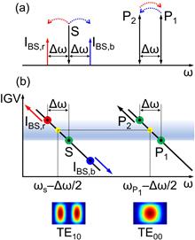
Intermodal four-wave mixing (FWM) processes have recently attracted significant interest for all-optical signal processing applications thanks to the possibility to control the propagation properties of waves exciting distinct spatial modes of the same waveguide. This allows, in principle, to place signals in different spectral regions and satisfy the phase matching condition over considerably larger bandwidths compared to intramodal processes. However, the demonstrations reported so far have shown a limited bandwidth and suffered from the lack of on-chip components designed for broadband manipulation of different modes. We demonstrate here a silicon-rich silicon nitride wavelength converter based on Bragg scattering intermodal FWM, which integrates mode conversion, multiplexing and de-multiplexing functionalities on-chip. The system enables wavelength conversion between pump waves and a signal located in different telecommunication bands (separated by 60 nm) with a 3 dB bandwidth exceeding 70 nm, which represents, to our knowledge, the widest bandwidth ever achieved in an intermodal FWM-based system.
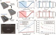
Silicon nitride (SiNx) is an appealing waveguide material choice for large-scale, high-performance photonic integrated circuits (PICs) due to its low optical loss. However, SiNx PICs require high electric power to realize optical reconfiguration via the weak thermo-optic effect, which limits their scalability in terms of device density and chip power dissipation. We report a 6-mode programmable interferometer PIC operating at the wavelength of 1550 nm on a CMOS-compatible low-temperature inductance coupled plasma chemical vapor deposition (ICP-CVD) silicon nitride platform. By employing suspended thermo-optic phase shifters, the PIC achieves 2× improvement in compactness and 10× enhancement in power efficiency compared to conventional devices. Reconfigurable 6-dimensional linear transformations are demonstrated including cyclic transformations and arbitrary unitary matrices. This work demonstrates the feasibility of fabricating power-efficient large-scale reconfigurable PICs on the low-temperature ICP-CVD silicon nitride platform.
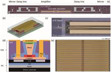
We demonstrate a III-V-on-silicon-nitride mode-locked laser through the heterogeneous integration of a semiconductor optical amplifier on a passive silicon-nitride cavity using the technique of micro-transfer printing. In the initial phase of our study, we focus on optimizing the lasing wavelength to be centered at 1550 nm. This optimization is achieved by conducting experiments with 27 mode-locked lasers, each incorporating optical amplifiers featuring distinct multiple-quantum-well photoluminescence values. Subsequently we present a comprehensive study investigating the behavior of the mode-locking regime when the electrical driving parameters are varied. Specifically, we explore the impact of the gain voltage and saturable absorber current on the locking stability of a tunable mode-locked laser. By manipulating these parameters, we demonstrate the precise control of the optical spectrum across a wide range of wavelengths spanning from 1530 to 1580 nm. Furthermore, we implement an optimization approach based on a Monte Carlo analysis aimed at enhancing the mode overlap within the gain region. This adjustment enables the achievement of a laser emitting a 23-nm-wide spectrum while maintaining a defined 10 dB bandwidth for a pulse repetition rate of 3 GHz.
We introduce a programmable eight-port interferometer with the recently proposed error-tolerant architecture capable of performing a broad class of transformations. The interferometer has been fabricated with femtosecond laser writing, and it is the largest programmable interferometer of this kind to date. We have demonstrated its advantageous error tolerance by showing an operation in a broad wavelength range from 920 to 980 nm, which is particularly relevant for quantum photonics due to efficient photon sources existing in this wavelength range. Our work highlights the importance of developing novel architectures of programmable photonics for information processing.
Self-injection locking has emerged as a crucial technique for coherent optical sources, spanning from narrow linewidth lasers to the generation of localized microcombs. This technique involves key components, namely a laser diode and a high-quality cavity that induces narrow-band reflection back into the laser diode. However, in prior studies, the reflection mainly relied on the random intracavity Rayleigh backscattering, rendering it unpredictable and unsuitable for large-scale production and wide-band operation. In this work, we present a simple approach to achieve reliable intracavity reflection for self-injection locking to address this challenge by introducing a Sagnac loop into the cavity. This method guarantees robust reflection for every resonance within a wide operational band without compromising the quality factor or adding complexity to the fabrication process. As a proof of concept, we showcase the robust generation of narrow linewidth lasers and localized microcombs locked to different resonances within a normal-dispersion microcavity. Furthermore, the existence and generation of localized patterns in a normal-dispersion cavity with broadband forward–backward field coupling is first proved, as far as we know, both in simulation and in experiment. Our research offers a transformative approach to self-injection locking and holds great potential for large-scale production.
The recent emergence of thin-film lithium niobate (TFLN) has extended the landscape of integrated photonics. This has been enabled by the commercialization of TFLN wafers and advanced nanofabrication of TFLN such as high-quality dry etching. However, fabrication imperfections still limit the propagation loss to a few dB/m, restricting the impact of this platform. Here, we demonstrate TFLN microresonators with a record-high intrinsic quality (Q) factor of twenty-nine million, corresponding to an ultra-low propagation loss of 1.3 dB/m. We present spectral analysis and the statistical distribution of Q factors across different resonator geometries. Our work pushes the fabrication limits of TFLN photonics to achieve a Q factor within 1 order of magnitude of the material limit.
The architecture and component technology of a low power, high capacity, short reach optical interconnect are detailed. Measurements from high-performance 300 mm silicon photonics components that comprise the system are shown, along with a quantum-dot mode-locked laser 20-channel comb source with free space wall plug efficiencies up to 17%, advanced packaging techniques for 3D silicon photonic-electronic integration, and schematics for integrated electronics that control the photonic integrated circuits. Techniques for operating such a system in the presence of changing ambient temperature are addressed. Experiments on a 1 Tbps design are conducted with an optical link experiment indicating sub-picojoule/bit energy consumption at scale.


