


Acousto-optical (AO) modulation is based on the coupling of multiple physical phenomena. Its principle lies in utilizing acoustic waves to manipulate the refractive index and boundary conditions of a medium, thereby enabling the modulation of optical signal frequency, intensity, and propagation direction. This technology has wide-ranging applications, including optical frequency shifting, non-reciprocal light transmission, beam deflection, and microwave filtering.
Conventionally, AO modulator depends on bulk piezoelectric materials, which makes the device bulky, expensive, and unsuitable for large-scale integration due to its weak acoustic confinement capabilities. The use of photonic integrated circuits has addressed this limitation by effectively confining optical waves within waveguide structures, and exciting acoustic waves through piezoelectric materials, which exhibits high AO overlap in a small range and achieves efficient modulation.
AO modulators based on various piezoelectric materials have been attracting increasing attention, such as lead zirconate titanate (PZT), gallium arsenide (GaAs), gallium nitride (GaN), lithium niobate (LN), and polycrystalline aluminum nitride (AlN). Among them, the fabrication process of AlN films is compatible with complementary metal-oxide-semiconductor (CMOS) technology, which has the potential to realize low-cost and high-performance AO modulators. Noticeably, the piezoelectric properties of AlN films can be significantly improved by doping with scandium (Sc) element, which has been widely demonstrated in the development of piezoelectric microelectromechanical systems (MEMS). In addition, scandium-doped aluminum nitride (AlScN) exhibits a wide electronic bandgap close to that of AlN, resulting a wide transparent window from ultraviolet to mid-infrared. Therefore, investigation of AO modulators based on AlScN is expected to promote the further development of on-chip AO devices.
In order to explore the potential of AO modulation based on thin-film AlScN, researchers from the Photonic Chip Lab (PCL) at Shanghai University present the first demonstration of AO modulators with surface acoustic waves generation and photonic waveguides integrated on a 400-nm-thick film of AlScN on an insulator (AlScNOI). Relevant research results were recently published in Photonics Research, Volume 12, No. 6, 2024. [Kewei Bian, Zhenyu Li, Yushuai Liu, Sumei Xu, Xingyan Zhao, Yang Qiu, Yuan Dong, Qize Zhong, Tao Wu, Shaonan Zheng, Ting Hu, "Demonstration of acousto-optical modulation based on a thin-film AlScN photonic platform," Photonics Res. 12, 1138 (2024)]
.png)
Figure 1 Schematic diagram of the devices.
Experimental results show that the devices demonstrate intramode AO modulation within a wide optical bandwidth (>20 nm). Due to the bidirectional propagation of acoustic surface waves excited by the interdigitated transducer, this research fully utilizes the bidirectional acoustic wave energy and increases the length of AO modulation by designing the interdigitated transducer at the center of a spiral waveguide. The modulation efficiency of the device is thereby increased by 12.3 dB. Researchers also demonstrated intermode AO modulation based on a multimode optical waveguide, which enables high-contrast (>10 dB) non-reciprocal AO modulation over an optical bandwidth of 0.48 nm. The devices proposed in this study exhibit robust mechanical stability and are fabricated using a process compatible with CMOS technology. This makes them well-suited for on-chip applications including narrowband microwave photonic filters, optical isolators, and optical circulators.
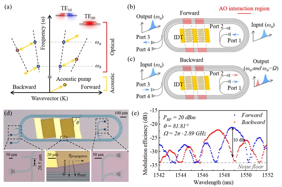
Figure 2 (a) The phase matching condition. (b) Forward direction: the probe light (blue) travels through the device without modulation. (c) Backward direction: the probe light is partly converted to the TE00 mode. (d) Micrograph of the AO modulator. (e) Non-reciprocal AO modulation.
Associate Professor Shaonan Zheng commented: This work verifies the feasibility of implementing AO modulators based on thin-film AlScN, providing new insights for research in this field and laying the foundation for AO devices based on this material platform. The fabrication process of this platform is compatible with CMOS technology, enabling low-cost, high-reliability wafer-level fabrication. By further investigating innovative structures and processes, the devices can achieve enhanced AO modulation efficiency and non-reciprocity. This advancement will have a positive impact on field of optical communications.
In the future, research team will optimize the etching process of AlScN thin films to reduce the propagation loss of waveguide. They will also try to improve the electromechanical coupling coefficient of the device by using AlScN with higher Sc concentrations and optimizing the substrate material. Furthermore, they aim to refine the parametric design of the device to achieve higher modulation efficiency. The research team hopes that the optimized devices will enrich the research in optical communication, sensing, and computing.