


Photonic integrated circuits (PICs) play a crucial role in optical computing, optical interconnects, and optical signal processing. Compared to traditional circuits, PICs often offer larger bandwidths, lower power consumption, and higher data rates. In recent years, PIC-based photonic chips have shown tremendous potential across various applications. With the increasing demands for PIC compactness, integration, and performance increases, there is a growing urgency to develop ultra-compact multifunctional integrated photonic modules. In photonic device design, inverse design based on various intelligent algorithms has emerged as a powerful approach. It often yields devices with significantly smaller footprints compared to conventional design methods, thus promoting the advancement of compactness for photonic devices and chips.
Despite the proposal of numerous high-compact photonic devices through inverse design, challenges persist in further developing ultra-compact multifunctional integrated photonic modules. These modules require excellent performance, ultra-high compactness, and complex functionalities, posing significant design difficulties, which increases demands on the optimization ability, efficiency, robustness (ability to overcome local convergence) of inverse design algorithms. To cope with current challenges faced by mainstream inverse design algorithms, the team has made innovations in underlying logic and proposed a new algorithm named polygon search (PS) algorithm, which enhances several algorithmic metrics. Utilizing the PS algorithm, they have designed a dual-channel mode-conversion-crossing waveguide (DCMC-CW) module that integrates two kinds of mode conversion and channel crossing within only 4×4 μm2 footprint, with each channel exhibiting insertion losses below 0.45 dB. Subsequently, combining this module with other PS-designed devices, they have constructed a high-performance, highly compact, and highly integrated PIC instance: a crossing-mode-division-multiplexing (CMDM) system. Relevant research results were recently published in Photonics Research, Volume 12, Issue 7, 2024. [Te Du, Zheng Peng, Peixin Huang, Zhaojian Zhang, Hansi Ma, Xinpeng Jiang, Jie Huang, Mingyu Luo, Hongxin Zou, Junbo Yang, "Polygon search algorithm for ultra-compact multifunctional integrated photonics design," Photonics Res. 12, 1527 (2024)]
In this study, the team first analyzed the underlying logic of several mainstream inverse design algorithms to identify their relative advantages. They discovered that some algorithms prevent the deterioration of the figure of merit (FOM) during optimization through the "trial and compare" search strategy, thereby enhancing optimization efficiency. On the other hand, many algorithms allow for wide and detailed shape exploration by setting the device as a continuous shape, achieving superior performance for complex devices. Therefore, the team considered introducing the "trial and compare" search strategy into the continuous-shape-optimizing framework to improve the design efficiency and effect simultaneously. Through careful design and extensive exploration, they proposed the PS algorithm, which combines excellent optimization capability with high design efficiency.
The basic principle of the PS algorithm is illustrated in Fig. 1. First, the designer sets the structure of the device to be designed as a polygon prism, with the base typically chosen as a simple, regular shape. Subsequently, the designer moves the first vertex of the prism base several times to search for a position that improves the FOM. This process continues sequentially for each vertex. After completing the search for all vertices, the designer assesses the results to determine whether to iterate again. In the search process of each vertex, the FOM keeps undeteriorating through the "trial and compare" strategy. Furthermore, leveraging the continuity of the polygon shape, the PS algorithm can utilize "approximate gradient prediction" or "neural network prediction" to enhance optimization efficiency and effectiveness: after searching multiple positions for a vertex, the PS algorithm can predict a position with a high probability of improving the FOM using approximate gradient or neural network.
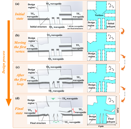
Fig. 1 Design process of a photonic device using the PS algorithm. The right figure of each subgraph represents the polygon base corresponding to the structure in the left figure of that subgraph. (a) Set the structure of the photonic device to be designed as a relatively simple and regular polygon prism; (b) Move the first vertex to search for a position that improves FOM. After searching for several positions, the PS algorithm can use approximate gradient or neural network to predict a position with highly probability of improving the FOM. (c) All vertices are searched once. Afterwards, the designer assesses the results to determine whether to iterate again. (d) Final structure designed by the PS algorithm after several loops.
Using their proposed PS algorithm, the team designed an ultra-compact, high-integration, and low-loss DCMC-CW module in this work, as depicted in Fig. 2(a). This module integrates three functions within only 4×4 μm2: mode conversion between TE0 and TE1, as well as TE0 and TE2, and channel crossing. Thus, a single or a combination of two modules can achieve low-loss mode conversion between TE0, TE1, and TE2, as shown in Fig. 2(b). Its introduction significantly enhances the compactness and integration of many PICs while improving their fabricating robustness. Subsequently, combining this module with PS-designed bending waveguides and PS-designed mode mixers, they constructed a CMDM optical interconnect system, illustrated in Fig. 2(c). This system provides various mode options and multi-mode multiplexing functionalities based on channel crossing, significantly increasing the communication bandwidth of PICs. Furthermore, focusing on the performance of the PS algorithm in broader photonic device design activities, the team provided a comprehensive contrast design experiment in this work. This experiment compares the design effect and efficiency of four algorithms, including the PS algorithm and three representative mainstream algorithms, under different initial conditions. The results show that compared to these mainstream algorithms, the PS algorithm achieves superior design effects, higher optimization efficiency, and broader adaptability.
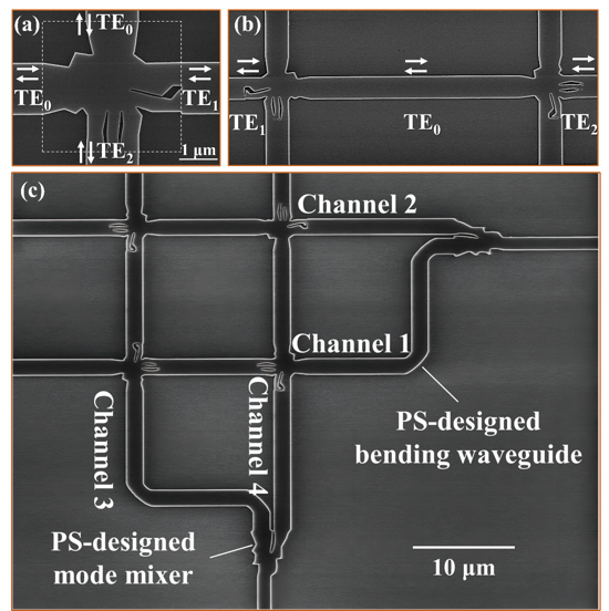
Fig.2 PS-designed module and system and the functions of them. (a) PS-designed ultra-compact, high-integration, and low-loss DCMC-CW module and its functions; (b) Mode interconversion between TE1 and TE2 achieved by two modules; (c) PS-designed CMDM system.
The team leader Junbo Yang said: "Enabling photonic chips with limited area to host more functions, exhibit stronger performance, and achieve higher iteration efficiency is a pursuit earnestly sought by the community. Developing ultra-compact, multifunctional integrated photonic modules and small-sized, high-performance integrated photonic circuits offers an excellent solution to these objectives. In recent years, the capability of inverse design algorithms to improve the compactness of photonic devices has been widely recognized. Therefore, leveraging inverse design to support the development of these modules and systems is an ideal choice."
The first author Te Du said: "In the past, inverse design algorithms based on different principles often presented similar design abilities, given the loose device size requirements and simple target functionalities. With the growing demand for high compactness and integration, there is now a higher requirement for the comprehensive design capability of inverse design algorithms. Our proposed PS algorithm not only integrates the advantages of different algorithms in underlying principle but also deeply integrates with neural networks, achieving exceptional design capability. Its emergence opens up richer possibilities for inverse-designed ultra-compact integrated photonics."
In the next step, the team will advance the research on two fronts. Firstly, they will continue to explore the potential of the PS algorithm to enhance its design capabilities. Secondly, utilizing the PS algorithm, the team will develop a series of highly practical ultra-compact, multi-functional integrated photonic devices and corresponding integrated systems, assisting the development of ultra-compact integrated photonics.