


Please enter the answer below before you can view the full text.
8-6=
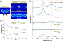
We theoretically investigate dark dimer mode excitation and strong coupling with a nanorod dipole. Efficient excitation of a dark mode in a gold (Au) nanorod dimer using an electric dipole can be achieved by an optimal overlap between the dipole moment and dark modal field. By replacing the dipole emitter with an Au nanorod, a plane wave excited dipole mode in the nanorod can be effectively coupled to the dark dimer mode through near-field interaction. At a 10-nm separation of the nanorod and the dimer, plasmonic interaction between dipole-dark modes enters the strong coupling regime with a Rabi-like splitting of 219.2 meV, which is further evidenced by the anticrossing feature and Rabi-like oscillation of electromagnetic energy of the coupled modes. Our results propose an efficient approach to far-field activating dark modes in coupled nanorod dimers and exchanging plasmonic excitations at nanoscale, which may open new opportunities for nanoplasmonic applications such as nanolasers or nanosensors.
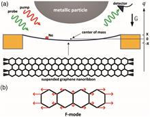
We propose an optical weighing technique with a sensitivity down to a single atom through the coupling between a surface plasmon and a suspended graphene nanoribbon resonator. The mass is determined via the vibrational frequency shift on the probe absorption spectrum while the atom attaches to the nanoribbon surface. We provide methods to separate out the signals of the ultralow frequency vibrational modes from the strong Rayleigh background, first based on the quantum coupling with a pump-probe scheme. Owing to the spectral enhancement in the surface plasmon and the ultralight mass of the nanoribbon, this scheme results in a narrow linewidth (~GHz) and ultrahigh mass sensitivity (~30 yg). Benefitting from the low noises, our optical mass sensor can be achieved at room temperature and reach ultrahigh time resolution.
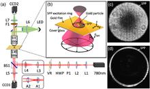
Strong plasmonic focal spots, excited by radially polarized light on a smooth thin metallic film, have been widely applied to trap various micro- and nano-sized objects. However, the direct transmission part of the incident light leads to the scattering force exerted on trapped particles, which seriously affects the stability of the plasmonic trap. Here we employ a novel perfect radially polarized beam to solve this problem. Both theoretical and experimental results verify that such a beam could strongly suppress the directly transmitted light to reduce the piconewton scattering force, and an enhanced plasmonic trapping stiffness that is 2.6 times higher is achieved in experiments. The present work opens up new opportunities for a variety of research requiring the stable manipulations of particles.
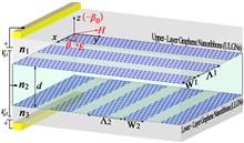
Near-field coupled plasmonic systems generally achieve plasmonically induced transparency (PIT) using only one-way bright–dark mode coupling. However, it is challenging to realize such well-designed devices, mainly because they depend significantly on the polarization direction. We exploit surface plasmons supported by two crossed layers of graphene nanoribbons (GNRs) to achieve dynamically tunable PIT, where each GNR operates as both the bright and dark modes simultaneously. The proposed PIT can result from either one-way bright–dark mode interactions or bidirectional bright–bright and bright–dark mode hybridized coupling when the polarization is perpendicular/parallel or at an angle to the GNRs, respectively. Additionally, identical ribbon widths yield polarization-insensitive single-window PIT, whereas different ribbon widths produce polarization-dependent double-window PIT. We examine the proposed technique using plasmon wave functions and the transfer matrix method; analytical and numerical results show excellent agreement. This study can provide physical insight into the PIT coupling mechanisms and advance the applicability and versatility of PIT-based sensing platforms and other active devices.
We show that Fourier-plane imaging in conjunction with the Kretschmann–Raether configuration can be used for measuring polariton dispersion with spatial discrimination of the sample, over the whole visible spectral range. We demonstrate the functionality of our design on several architectures, including plasmonic waveguides, and show that our new design enables the measurement of plasmonic dispersion curves of spatially inhomogeneous structures with features as small as 3 μm, in a single shot.
Although plasmonic nanostructure has attracted widespread research interest in recent years, it is still a major challenge to realize large-scale active plasmonic nanostructure operation in the visible optical frequency. Herein, we demonstrate a heterostructure geometry comprising a centimeter-scale Au nanoparticle monolayer and VO2 films, in which the plasmonic peak is inversely tuned between 685 nm and 618 nm by a heating process since the refractive index will change when VO2 films undergo the transition between the insulating phase and the metallic phase. Simultaneously, the phase transition of VO2 films can be improved by plasmonic arrays due to plasmonic enhanced light absorption and the photothermal effect. The phase transition temperature for Au/VO2 films is lower than that for bare VO2 films and can decrease to room temperature under the laser irradiation. For light-induced phase transition of VO2 films, the laser power of Au/VO2 film phase transition is ~28.6% lower than that of bare VO2 films. Our work raises the feasibility to use active plasmonic arrays in the visible region.
Aggregation of metal nanoparticles plays an important role in surface enhanced Raman scattering (SERS). Here, a strategy of dynamically aggregating/releasing gold nanoparticles is demonstrated using a gold-nanofilm coated nanofiber, with the assistance of enhanced optical force and plasmonic photothermal effect. Strong SERS signals of rhodamine 6G are achieved at the hotspots formed in the inter-particle and film-particle nanogaps. The proposed SERS substrate was demonstrated to have a sensitivity of 10 12 M, reliable reproducibility, and good stability.
Optical trapping techniques are of great interest since they have the advantage of enabling the direct handling of nanoparticles. Among various optical trapping systems, photonic crystal nanobeam cavities have attracted great attention for integrated on-chip trapping and manipulation. However, optical trapping with high efficiency and low input power is still a big challenge in nanobeam cavities because most of the light energy is confined within the solid dielectric region. To this end, by incorporating a nanoslotted structure into an ultracompact one-dimensional photonic crystal nanobeam cavity structure, we design a promising on-chip device with ultralarge trapping potential depth to enhance the optical trapping characteristic of the cavity. In this work, we first provide a systematic analysis of the optical trapping force for an airborne polystyrene (PS) nanoparticle trapped in a cavity model. Then, to validate the theoretical analysis, the numerical simulation proof is demonstrated in detail by using the three-dimensional finite element method. For trapping a PS nanoparticle of 10 nm radius within the air-slot, a maximum trapping force as high as 8.28 nN/mW and a depth of trapping potential as large as 1.15×10⁵ kBT mW 1 are obtained, where kB is the Boltzmann constant and T is the system temperature. We estimate a lateral trapping stiffness of 167.17 pN·nm 1· mW 1 for a 10 nm radius PS nanoparticle along the cavity x-axis, more than two orders of magnitude higher than previously demonstrated on-chip, near field traps. Moreover, the threshold power for stable trapping as low as 0.087 μW is achieved. In addition, trapping of a single 25 nm radius PS nanoparticle causes a 0.6 nm redshift in peak wavelength. Thus, the proposed cavity device can be used to detect single nanoparticle trapping by monitoring the resonant peak wavelength shift. We believe that the architecture with features of an ultracompact footprint, high integrability with optical waveguides/circuits, and efficient trapping demonstrated here will provide a promising candidate for developing a lab-on-a-chip device with versatile functionalities.
Natural surface-enhanced Raman spectroscopy (SERS) chips based on plants or insects have gained increased attention due to their facile characteristics and low costs. However, such chips remain a major challenge for practical application because of poor reproducibility and stability as well as unavoidable damage to the surface structure during coating metal and uncontrolled dehydration. By using a simple wrinkling method, we develop a new route to fabricate a low-cost bionic SERS chip for practical detection. Inspired by the taro leaf, we fabricate a SERS chip with a super-hydrophobic and plasmonic micro/nano dual structure, and its structure parameters can be optimized. Compared with the natural taro-leaf SERS chip, our artificial chip exhibits Raman signals with an order of magnitude higher sensitivity (~10 9 M) and enhancement factor (~107) under the illumination of weak laser radiation, demonstrating that our SERS chip has great potential in biological detection. The excellent performances of our bionic SERS chip are attributed to a synergy of optimized micro-wrinkle and nano-nest, which is verified by experiment and simulation. We believe our bionic chip could be a promising candidate in practical application due to its merits such as simple fabricating process, optimizable structure, low cost, excellent homogeneity, high sensitivity, and stability.
We have used a gold nanohole array to trap single polystyrene nanoparticles, with a mean diameter of 30 nm, into separated hot spots located at connecting nanoslot regions. A high trap stiffness of approximately 0.85 fN/(nm·mW) at a low-incident laser intensity of ~0.51 mW/μm2 at 980 nm was obtained. The experimental results were compared to the simulated trapping force, and a reasonable match was achieved. This plasmonic array is useful for lab-on-a-chip applications and has particular appeal for trapping multiple nanoparticles with predefined separations or arranged in patterns in order to study interactions between them.
The plasmonic nanogap antenna is an efficient radiating or receiving optical device. The resonance behavior of optical antennas is commonly attributed to the excitation of a localized surface plasmon resonance (LSPR), which can be theoretically defined as the quasi-normal mode (QNM). To clarify the physical origin of the LSPR, we build up an analytical model of the LSPR by considering a multiple scattering process of propagative surface plasmon polaritons (SPPs) on the antenna arms. The model can comprehensively reproduce the complex eigenfrequency and the field distribution of QNMs of the antenna, unveiling that the LSPR arises from a Fabry–Perot resonance of SPPs. By further applying the complex pole expansion theorem of meromorphic functions, the field of the antenna under illumination by a nearby dipole emitter can be analytically expanded with QNMs, which well predicts the frequency response of the enhancement factor of radiation. The present model establishes explicit relations between the concepts of the LSPR and the propagative SPP and integrates the advantages of the Fabry–Perot and QNM formalisms of nanogap antennas.
We suggest a low cross-talk plasmonic cross-connector based on a metal/insulator/metal cavity and waveguides. We separately investigate the isolated cavity mode, the waveguide mode, and the combination of cavity and waveguide modes using a finite-different time-domain method. Due to resonant tunneling and the cutoff frequency of the odd waveguide mode, our proposed structure achieves a high throughput transmission ratio and eliminates cross-talk. Furthermore, the proposed structure has a broadband tunability of 587 nm, which can be achieved by modulating the cavity air gap thickness. This structure enables the miniaturization of photonic integrated circuits and sensing applications.
In this paper we present a novel nanoantenna (nantenna) design for energy harvesting. The nantenna has an “E” shape and is placed on a SiO2 substrate. Its operation is based on the excitation of surface plasmon polaritons through the gold arms of the E shape. By varying the lengths and widths of the arms, two overlapping working bandwidths can be achieved. This results in a wideband behavior characterized by a full width at half-maximum of about 2.2 μm centered around 3.6 μm. Two orthogonal E nantennas are placed perpendicular to each other to realize a dual-polarized nantenna. This nantenna can receive the two incident polarizations at two separate gap locations with very high isolation. The proposed structure can be used in several energy harvesting applications, such as scavenging the infrared heat from the Earth and other hot objects, in addition to optical communications.crystals;Subwavelength structures, nanostructures;Resonance
A tunable plasmonic perfect absorber with a tuning range of ~650 nm is realized by introducing a 20 nm thick phase-change material Ge2Sb2Te5 layer into the metal–dielectric–metal configuration. The absorption at the plasmonic resonance is kept above 0.96 across the whole tuning range. In this work we study this extraordinary optical response numerically and reveal the geometric conditions which support this phenomenon. This work shows a promising route to achieve tunable plasmonic devices for multi-band optical modulation, communication, and thermal imaging.
Coupled plasmonic nanoparticles of Au and nanorods of ZnTe are modeled and fabricated. Full-wave simulation is performed to obtain an optimum design for enhanced light absorption and to explain scattering properties of the structure. The fabrication method of such arrays is described. Modeling the spectral properties using equivalent circuit theory is also implemented to provide an intuitive approach regarding the design of optical metamaterials with predetermined properties.