


Please enter the answer below before you can view the full text.


2024
Volume: 61 Issue 11
20 Article(s)

Tianxin Wang, and Yong Zhang
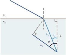
The evolution of integrated optoelectronic devices has transitioned from conventional two-dimensional configurations to full spatial dimensions. Laser direct writing, with its unique three-dimensional processing capabilities, has significantly contributed to the advancement of photonic chips. Lithium niobate has garnered considerable interest due to its excellent material properties. Nonetheless, the large refractive index mismatch at the interface between lithium niobate and air considerably affects the accuracy of laser direct writing within lithium niobate crystals. Adaptive optics-based aberration correction emerges as a practical approach to address this challenge. In this study, we begin with an analysis of the point spread function and proceed to derive theoretical precompensation functions. In experiments, we employ a spatial light modulator to implement aberration correction. We systematically compare and characterize grating structures processed with and without aberration correction. Employing aberration correction at a depth of 110 μm beneath the surface results in the formation of uniform laser-modified structures devoid of focal subpoints. The incorporation of adaptive optics into the laser direct writing process paves the way for the fabrication of high-quality three-dimensional photonic structures within lithium niobate crystals.
Jun. 10, 2024Vol. 61 Issue 11 1116001 (2024)
Zijun Huang, Rui Ma, and Xinlun Cai
Optoelectronic oscillators (OEOs) can generate high frequency, broadband tunable, and low phase noise radio frequency (RF) signals that can be applied in 5G communication, radar detection, and sensing. The basic structure of an OEO includes lasers, modulators, energy storage media, photodetectors, RF amplifiers, and RF filters. The key to achieve low phase noise is high-Q energy storage media, such as low loss long fibers or high-Q optical resonators. As Dr. Yao Xiaotian proposed OEOs in 1996, various OEO structures have emerged; however, a majority of these are composed of discrete devices, making them bulky, expensive, and inconvenient to use. With the development of various integrated optical material platforms, it has become possible to construct small-sized, low-cost, and more reliable integrated OEOs, such as silicon-on-insulator (SOI), indium phosphide, and chalcogenide OEOs. However, due to high loss, nonlinearity, and temperature sensitivity of these materials, it is difficult to achieve the high-performance electro-optic modulators and high-Q energy storage media required for OEOs. Consequently, thin-film lithium niobate (TFLN) has been widely used for achieving high-performance electro-optic modulators and high-Q microcavities due to its wide transparent window, large linear electro-optic coefficient, and low loss characteristics; thus, it achieves high frequency, broadband tunable, and low phase noise RF signals. This article reviews the development process of OEOs over the past 30 years, from discrete OEOs to integrated OEOs. It also discusses future development prospects of integrated OEOs.
Jun. 10, 2024Vol. 61 Issue 11 1116002 (2024)
Haoyang Du, Xiuquan Zhang, Lei Wang, and Feng Chen
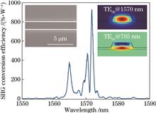
Difference-frequency generation enables optical nonlinear-wavelength conversion and is vital for generating coherent light at long wavelengths. In this study, we demonstrate modal-phase-matched difference-frequency generation on a thin-film lithium-niobate platform. By varying the wavelength of the signal light, difference-frequency generation is realized across the entire spectrum of the signal laser. In addition, by manipulating the power of the signal light coupled into the waveguide, an on-chip conversion efficiency of 188 %·W-1 is achieved. Experimental results show that the proposed method is promising for multiwavelength frequency conversion in optical communication and future all-optical communication networks.
Jun. 10, 2024Vol. 61 Issue 11 1116003 (2024)
Yonghui Tian, Mingrui Yuan, Shijing Qin, Hao Li, Sixuan Wang, and Huifu Xiao
Due to their excellent electro-optic, acousto-optic, and nonlinear optical properties, lithium niobate (LiNbO3) materials are widely recognized as ideal platforms for developing high-performance integrated optoelectronic chips. In recent years, advancements in micro-nano processing technology and successful fabrication of wafer-scale lithium niobate on insulator (LNOI) thin films have led to substantial advantages in integrating large-scale high-speed optoelectronic device on the LNOI platform. With the successful realization of fundamental communication devices such as high-speed modulators that utilize optoelectronic integration technology, increased attention has been given to advanced multiplexing techniques that extend data capacity by transmitting multiple channels in parallel. In the LNOI platform, various integrated photonic devices based on multiple multiplexing dimensions have been developed with the aim of achieving monolithic integration of high-speed and large-capacity optoelectronic communication devices. This paper explores LNOI waveguides and recently reported multi-dimensional multiplexed LNOI integrated photonic devices, including key technologies such as optical signal multiplexing, manipulation, and control in wavelength, mode, and polarization dimensions. We also detail the working mechanisms, design principles, methods, and performance parameters of the devices. Finally, this paper discusses the current challenges and potential solutions for implementing multi-dimensional multiplexed integrated photonic devices in the LNOI platform.
Jun. 10, 2024Vol. 61 Issue 11 1116004 (2024)
Yawen Su, Haiwei Chen, Mengwei Zhao, Yunfei Niu, Chen Li, Yong Zhang, Shaoguang Yang, Shining Zhu, and Xiaopeng Hu
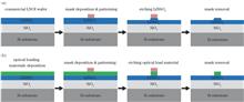
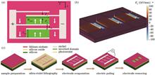
Conductive ferroelectric domain walls have attracted increasing research interest in the field of nanoelectronics, and the fabrication technique for such domain walls is vital. In this study, we investigated in detail the fabrication of conductive domain walls in x-cut congruent thin-film lithium niobate (TFLN) using an electrical-field poling technique. The ferroelectric domain structures can be controlled through the applied electrical field and applied pulse numbers, and the domain inversion process is related to the conduction characteristics of the domain walls. The domain structures in TFLN are revealed using confocal second-harmonic microscopy and piezoresponse force microscopy. The results provide further directions for the development and application of conductive domain walls in TFLN.
Jun. 10, 2024Vol. 61 Issue 11 1116005 (2024)
Zong Wang, Guanyu Chen, Yu Yu, and Xinliang Zhang
A polarization-independent electro-optical modulator based on thin-film lithium niobate (TFLN) is proposed; it is based on a polarization-independent beam splitter and a mode converter. The polarization-independent beam splitter achieves precise beam splitting of TE0 and TM0 modes, whereas the mode converter efficiently converts the input TM0 mode to TE1 mode. Accordingly, the traveling-wave electrode structure loaded with periodic capacitors achieves efficient electro-optical modulation of two light modes. The simulation results show that the electro-optical bandwidth of the modulator is greater than 100 GHz. This helps solve the instability problem caused by polarization sensitivity in existing electro-optical modulators and opens up new research lines for TFLN-based modulators.
Jun. 10, 2024Vol. 61 Issue 11 1116006 (2024)
Haoyang Zhang, Zuoxin Kuang, Guanyu Chen, and Hua Yu
Due to the influence of inherent characteristics of material, the bias operating point of electro-optic modulator may drift with changes in environment, thereby affecting the modulation performance of the modulator. To solve the bias point drift issue of lithium niobate Mach-Zehnder electro-optic modulators, bias control techniques suitable for 4-array parallel electro-optic modulators is researched. Based on time division multiplexing, adjustable gain amplitude, dual pattern recognition, and other methods, a control method combining optical power and disturbance signal amplitude detection is proposed, which reduces hardware redundancy and achieves precise control of the bias operating point.
Jun. 10, 2024Vol. 61 Issue 11 1116007 (2024)
Jiying Huang, Lei Wan, Chengyu Chen, Yuping Chen, and Zhaohui Li
Surface acoustic wave-driven on-chip integrated acousto-optic modulators have become the critical technique in microwave-to-optical conversion due to their small footprint, high efficiency, low power consumption, and easy integration. In this paper, we summarize the recent progress of thin-film lithium niobate (TFLN) acousto-optic modulators, and mainly focus on their applications in microwave photon information processing. First, we introduce the basic principles of the TFLN acoustic-optic modulators. Then, we review the key research achievements in recent years, including the improvement and optimization of performance parameters such as modulation speed, modulation efficiency, and optomechanical coupling rate. Lastly, we discuss the potential applications of TFLN acousto-optic modulators with respect to the filter, frequency shifter, LiDAR, optical isolator, and microwave-optical conversion. The development trends of the TFLN acousto-optic modulators in the future are also briefly provided.
Jun. 10, 2024Vol. 61 Issue 11 1116008 (2024)
Shiyao Deng, Jiahao Peng, Libo Wang, Runhao Liu, Fangheng Fu, Huajiang Chen, Yuming Wei, Tiefeng Yang, Heyuan Guan, and Huihui Lu
Electric field sensors have broad application prospects in the fields of automobiles, avionics, medical equipment, power systems, and high-energy physics research. They are also of great significance in the fields of engineering technology and scientific research. This study introduces several working principles of electric field sensors and provides a comparative analysis of the advantages of electric field sensors based on the lithium niobate electro-optic effect. The working principles of the integrated optical waveguide Mach-Zehnder structure and the microstructural electric field sensor based on resonance peak drift are derived. This study furthers summarizes and analyzes the recent research progress of electric field sensors of the lithium niobate bulk crystal type and thin-film lithium niobate type. The study also focuses on the improvement of sensor structure in sensitivity, linear dynamic range, frequency response, device size and other performance indicators and key technologies. The challenges and prospects for the future development of electric field sensors based on the lithium niobate electro-optic effect are also explored.
Jun. 10, 2024Vol. 61 Issue 11 1116009 (2024)
Yi Ni, Yu Lin, Yin Xu, and Yedeng Fei
This study proposes a large bandwidth two-dimensional grating coupler based on the lithium niobate platform. By introducing a lithium niobate crystal comprising a photoelectric material as the platform, a silicon triangle structure is adopted, and based on the effective medium theory, the transverse width of each triangle is changed along the direction of light propagation. A low refractive index oxide buffer layer is introduced between the silicon grating coupler and the bottom of lithium niobate thin film (LNTF) waveguide. A vertical grating coupler with a coupling efficiency of 60.8% and a 1 dB bandwidth of 102 nm is obtained at a wavelength of 1550 nm.
Jun. 10, 2024Vol. 61 Issue 11 1116010 (2024)
Li Deng, Renhong Gao, Jianglin Guan, Chuntao Li, Guanghui Zhao, Minghui Li, and Qian Qiao
Thin-film lithium niobate (TFLN) micro/nano-structures allowing strong light field confinement to boost the interaction between light and matter, shows great potentials for cutting-edge researchs and high-tech applications for high speed optical communications, high-performance optical computation, integrated photonics, and integrated quantum information processing, etc. This article reviews the basic principles, manufacturing technical advances, and the latest progress of TFLN microdevices based on microresonators and waveguides, including various applications ranging from frequency conversion, electro-optic modulation, optical frequency combs to microwave-to-optical wave conversion, quantum photonics, and microlasers. The application of these techniques has greatly promoted the development of large-scale integrated optoelectronic circuits and quantum networks. In addition, this article gives a perspective on potential applications in the future.
Jun. 10, 2024Vol. 61 Issue 11 1116011 (2024)
Shixin You, Chenzhi Yuan, and Ruibo Jin
Lithium niobate crystal satisfies the group-velocity-matching condition in 3.2 μm wavelength band, enabling the generation of spectrally uncorrelated biphotons through spontaneous parametric down-conversion (SPDC). However, under this condition, the biphotons typically exhibit an annular distribution in the spatial domain, resulting in reduced photon collection efficiency and diminished source brightness. Therefore, achieving the frequency-uncorrelated and spatial-single-mode states has become an urgent problem that needs to be addressed. In this study, through theoretical calculations and numerical simulations, the spatial distribution of biphotons was optimized.It was found that under specific wavelength and temperature conditions, the two-photons generated in SPDC by periodically polarized lithium niobate and custom polarized lithium niobate can exhibit a beam like distribution in space, with Schmidt number of 1.170 and 1.150. This approach offers a solution for quantum optical experiments in the mid-infrared wavelength range, by providing quantum light sources with frequency-uncorrelated and spatial single-mode characteristics.
Jun. 10, 2024Vol. 61 Issue 11 1116012 (2024)
Yanan Wen, Zhenyuan Lin, and Lingfei Ji
Through femtosecond laser single-pulse experiments, we investigated the influence of polarization directions (0°, 45°, 90°, and 135°) on the damage threshold of x-cut lithium niobate (LN) crystals. We found that the material damage threshold exhibited considerable polarization dependence, with the damage threshold along the 90° polarization direction being lower than those in other polarization directions. Through first-principles calculations, we confirmed that tunneling ionization caused by the femtosecond laser mainly breaks Nb—O bonds. Along the incident polarization angle of 90°, more number of Nb—O bonds are easily broken, thereby reducing the damage threshold in that polarization direction. This study contributes to an in-depth understanding of the ablation of ultrafast lasers on LN crystal surfaces and has an important reference value for the laser preparation of functional devices on LN crystal surfaces.
Jun. 10, 2024Vol. 61 Issue 11 1116013 (2024)
Yipeng Lun, Xingzhao Huang, Yantong Li, Huakang Yu, and Zhiyuan Li
The transverse frequency-resolved optical gating (T-FROG) method based on a thin-film lithium niobate waveguide platform was previously proved to enable the accurate, in situ, and full-parameter characterization of waveguided femtosecond pulses inside integrated circuits. Herein, we confirm that the T-FROG method can operate over broadband spectra (e.g., 150 nm), which are benefited by the broadband operation characteristic features of transverse second-harmonic generation. Experimental results indicate that this method exhibits high sensitivity and signal-to-noise ratio for measuring pulses of various wavelengths. Furthermore, the proposed approach is applied to measure unknown pulses generated from a photonic crystal fiber, and the result indicates its potential for characterizing complex pulses.
Jun. 10, 2024Vol. 61 Issue 11 1116014 (2024)
Yi Ni, Jun Xia, and Yedeng Fei
Due to the increasing demand for dynamically reconfigurable properties in building intelligent optical interconnects, a reconfigurable polarization beam splitter (PBS) on a lithium-niobate-on-insulator (LNOI) platform using a triple-waveguide coupler was implemented. The output port of the transverse magnetic (TM) mode can be controlled by adjusting the phase state of the optical phase change material (PCM) to realize the reconfigurable function. A 3D finite difference time domain (3D-FDTD) method was also employed to investigate the performance and to optimize the structure of the PBS. The results show that the TM and transverse electric (TE) modes can be efficiently separated when PCM is in the amorphous state, where the extinction ratio exceeds 20 dB in the wavelength range of 1530?1580 nm under the TM mode and an ultra-low insertion loss is incurred under the TE mode (approximately 0.03 dB). When the PCM switches into the crystalline state, the TM and TE modes transmit along the input waveguide, and the reconfigurable function is enabled, where the size is 35 μm, which is compact for integration. Finally, the fabrication tolerance of the device is investigated, and the results indicate a certain degree of robustness.
Jun. 10, 2024Vol. 61 Issue 11 1116015 (2024)
Di Jia, Zhenzhong Hao, Fang Bo, Guoquan Zhang, and Jingjun Xu
Thin-film lithium niobate (TFLN) exhibits excellent electro-optic and optical nonlinear properties, and is an important platform for research on electro-optic modulators and nonlinear optical frequency converters. However, the significant difference in mode field sizes between the optical waveguides on TFLN films and optical fibers severely restricts efficient coupling between them. Consequently, high efficiency end couplers are valuable for breaking through the application bottleneck of TFLN-integrated optical chips. In this paper, a systematic review of the research progress of TFLN edge couplers is presented. First, the common characteristics of optical fibers involved in edge coupling are introduced. Subsequently, the typical structures of lithium niobate edge-coupling waveguides, such as single layer or multilayer inverse-tapered waveguides and wedge waveguides, are discussed. The selection and fabrication methods for related cladding materials are also described. Finally, the current research status and existing challenges in using edge couplers are summarized, and directions for potential future development are proposed.
Jun. 10, 2024Vol. 61 Issue 11 1116016 (2024)
Hao Yao, Mengke Wang, Jiayao Deng, Yuzhe Sun, Jieyun Wu, and Kaixin Chen
Lithium niobate has been widely used in the fabrication of high-performance electro-optic waveguide modulators and switches in the past decades because of its wide transparent window, mature waveguide fabrication technologies, and remarkable electro-optic effect. In recent years, with the advent of high-quality commercialized thin film lithium niobate, a variety of high-performance thin film lithium niobate optical waveguide devices have been demonstrated experimentally, and the performance of these devices has far exceeded their counterpart fabricated with conventional bulk lithium niobite wafer. In this paper, the progress of optical waveguides, couplers, electro-optical modulators, and tunable filters on thin-film lithium niobate platforms in recent years are reviewed, and the challenges faced by thin-film lithium niobate waveguide devices are briefly discussed.
Jun. 10, 2024Vol. 61 Issue 11 1116017 (2024)
Tian Gao, Ranfeng Gan, Bin Chen, Jiayang Yu, Jie Liu, Changjian Guo, Kaixuan Chen, and Liu Liu
Due to the anisotropy of the x-cut thin-film lithium niobate optical integration platform, the transverse magnetic (TM) mode of the optical waveguide is prone to mode hybridization and coupling to other modes during bending, posing a challenge to the bending of the TM mode. This article takes a 400 nm thick, semi-etched lithium niobate waveguide as an example to analyze the mode hybridization phenomenon of TM0 mode under different waveguide widths and transmission directions, and simulates its 90° bending transmission performance. The findings indicate that within a certain waveguide width range (approximately 1.7 μm to 2.15 μm), no mode hybridization occurs when bending the TM0 mode. However, for waveguide width lower than 1.7 μm or higher than 2.15 μm, coupling between the TM0 and TE1 (or TE2) mode occurs. Experimental demonstrations further corroborate this conclusion. This study offers a design methodology for achieving TM mode bending in thin-film lithium niobate waveguides, with potential applications in polarization-control-related optical integrated devices on this platform.
Jun. 10, 2024Vol. 61 Issue 11 1116018 (2024)
Moyang Kong, Hanghang Yu, and Tianwu Wang
This study proposes a co-linear scheme for generating strong terahertz radiation in a lithium niobate source using a contact grating method. This scheme achieves co-linearity between the incidence direction of pump light and the radiation direction of terahertz wave, thereby directly eliminating the complex angle adjustment required in traditional tilted-pulse-front technologies. Moreover, the scheme has a compact structure, simple optical path, and high radiation efficiency, laying a strong foundation for the widespread application of lithium niobate terahertz sources. We analyze the design of the contact-grating structure and the nonlinear interactions within the lithium niobate crystal using structural simulation, theoretical derivation, and numerical simulation. Further, we derived optimized grating structure parameters and obtained the radiation field intensity distribution of terahertz waves propagating inside the lithium niobate crystal. The simulation results show that the terahertz radiation energy reaches its maximum value after the pump light propagates a certain distance. This simulation obtained the position of the maximum value and determined the optimal thickness of the crystal, providing a reference for the production of lithium niobate strong terahertz radiation sources.
Jun. 10, 2024Vol. 61 Issue 11 1116019 (2024)
Jinlong Lu, Ting Hao, Zhihao Li, Dennis Zhou, and Guijun Ji
Using multi-physics simulations, this study compares the temperature distributions, modulation efficiencies, and transient responses of a thermo-optical phase-shifter across three thin-film lithium niobate (TFLN) waveguides equipped with different heating circuits. The results reveal that the TFLN thermo-optical phase-shifter exhibits optimal modulation efficiency when the heating circuit is installed directly above the central waveguide. Alternatively, heating circuits with multiple resistors yield similar modulation efficiencies with reduced thermal crosstalk, making them particularly suitable for localized modulation in scenarios necessitating the integration of multiple waveguides. Three-dimensional multi-physics simulation results demonstrate a reasonable thermal modulation efficiency (approximately 34 mW) of the thermo-optical phase-shifter with a transient response time of approximately 180 μs.
Jun. 10, 2024Vol. 61 Issue 11 1116020 (2024)
© Copyright 2018-2021 | Chinese Laser Press.
All Rights Reserved 沪ICP备15018463号-20