


Please enter the answer below before you can view the full text.


2025
Volume: 54 Issue 5
21 Article(s)

Xinyu ZHANG, Jin WANG, Jie XUE, and Bing ZHU
Orbital Angular Momentum (OAM) beams, with their theoretically infinite topological charge and orthogonality, demonstrate significant potential for enhancing the capacity of communication systems. In OAM Free-Space Optical (FSO) communication systems, atmospheric turbulence acts as a significant technical bottleneck, causing optical wavefront distortion and leading to effects such as scintillation, beam expansion, beam wander, and arrival angle fluctuation. These effects reduce the recognition accuracy of OAM beam topological charges, thereby increasing the bit error rate in OAM-FSO systems. To address this, a deep learning-based approach utilizing Convolutional Neural Networks (CNNs) has emerged, capturing OAM beam intensity images after turbulence transmission via Charge-Coupled Devices (CCDs). However, the recognition speed is constrained by the low frame rate of area array CCDs and the relatively slow processing speed of deep learning on PC. CCD cameras typically operate at tens of Hz, while PC-side data processing rates are generally in the kHz range, which is insufficient for high-speed OAM-FSO communication applications.This paper proposes a novel recognition scheme to improve CNN recognition speed. The scheme employs a cylindrical lens and Photodiode Array (PDA) to convert the two-dimensional intensity signal of superimposed OAM light fields into a one-dimensional signal, thereby reducing the computational complexity. A one-dimensional CNN is implemented on a Field-Programmable Gate Array (FPGA), referred to as CNN-FPGA, enabling high-speed signal processing and recognition. The scheme is theoretically analyzed using the Hill-Andrews model and random phase screen simulations. The same dataset is used to train and test both the refined CNN, referred to as model2, and a conventional CNN. The model2 achieves 99.0% recognition accuracy in a 200-m channel with a turbulence intensity of Cn2=5×10-15 m-2/3, requiring only 576 floating-point operations (Flops), while the conventional CNN achieves 99.9% accuracy under the same conditions but with 67 520 Flops. Although the refined CNN's accuracy is slightly lower, it remains within the effective recognition range, and lower bit error rates can be achieved using coding techniques. To evaluate the adaptability of the trained model2 to atmospheric turbulence disturbances of varying intensities, the recognition accuracy of model2 for OAM optical signals under different turbulence conditions was simulated using six training parameters. The simulation results demonstrate that the trained model2 exhibits strong adaptability to atmospheric turbulence disturbances across a range of intensities. In the experimental process, the superimposed OAM beams with topological charges l=±1,±2,±3,±4 are generated using digital holography. To determine the turbulence intensity during the CNN-based recognition of superimposed OAM optical signals in the experiment and compare it with simulation results, the atmospheric turbulence intensity at the experimental site was measured using the angle-of-arrival fluctuation method. The OAM transmission recognition experiments conducted in a 200-m outdoor environment, approximately 3 h after sunset with an atmospheric refractive index structure constant Cn2 on the order of 10-17 m-2/3, demonstrated a recognition accuracy exceeding 93.5%. Compared with simulation results, both the experiment and simulation exhibit a consistent trend of decreasing recognition accuracy with increasing turbulence intensity. The CNN-FPGA exhibits a maximum logic delay of 5.4 ns and a net delay of 12.6 ns within the FPGA chip, resulting in a shortest clock period of 0.018 μs. Compared to CPU and GPU platforms, the FPGA achieves comparable recognition accuracy while offering the fastest inference speed, the lowest cost and power consumption, and a more compact design with enhanced portability. The proposed scheme integrates a high-speed PDA module, optoelectronic signal processing circuit, analog-to-digital converter, and FPGA-based CNN module, achieving a recognition time of 0.072 μs per OAM signal, which greatly improve the recognition rate of optical communication systems. This scheme provides an efficient and practical technical solution for OAM optical signal recognition in FSO communication systems, which holds reference significance for the development and application of OAM-FSO communication technology.
May. 25, 2025Vol. 54 Issue 5 0501001 (2025)
Fuyou WANG, Xiaolei WANG, Zhenni LI, Xiaoquan SONG, and Long YUN
Atmospheric visibility refers to the maximum distance at which a person with normal vision can discern and identify a target object against the sky background. It plays a crucial role in aviation, maritime navigation, traffic safety, meteorological observation, and air pollution research. Remote sensing technology has long been a key focus for visibility monitoring. Compared to conventional visibility sensors, lidar has demonstrated significant advantages, including high spatiotemporal resolution, real-time data acquisition, and the capability for single-end detection. These advantages make lidar a promising tool for visibility observation.This study reviews existing visibility measurement methods, highlighting previous research on visibility monitoring using lidar. It further explores a visibility retrieval method based on coherent Doppler wind lidar. A field experiment was conducted in the Shiyan region of Shenzhen from September 9 to October 6, 2019. A coherent Doppler wind lidar was operated alongside the Shenzhen Meteorological Tower for joint observations. The meteorological tower was equipped with nephelometers at three different heights to provide truth visibility measurements.The backscatter intensity measured by the coherent Doppler wind lidar, along with the horizontal visibility and Relative Humidity (RH) data recorded by the nephelometer and its humidity sensor, were utilized to perform nonlinear fitting based on theoretical analysis. To verify the effectiveness of the fitting method, the collected data was divided into training and testing datasets in chronological order. The training data spanned from September 9 to October 1, 2019, while the testing period covered October 2 to October 6, 2019.With training data, a natural logarithm relationship model was established between horizontal visibility and lidar backscatter intensity. This model was then applied to estimate and validate the visibility measurements in the testing dataset. The experimental results indicate that at heights of 50 m and 100 m, both correlation coefficients between the lidar-derived visibility estimates and the observed values exceed0.83 in the testing dataset. These findings demonstrate that coherent Doppler wind lidar offers high accuracy and reliability for visibility measurement, making it a viable alternative to traditional methods. Additionally, to eliminate potential outliers, a 90% confidence interval was applied to filter residual data, further improving the correlation coefficient. This refinement process underscored the robustness of the model and its ability to enhance the precision of lidar-based visibility estimation.Furthermore, based on the classification criteria for fog and haze, the observational data was divided into two categories: one with RH greater than or equal to 80% and the other with RH below 80%. Separate fitting functions were developed for each category, followed by an analysis of their respective characteristics. The classified lidar backscatter intensity data was then used to estimate horizontal visibility for both groups. The results indicate that when RH is below 80%, the correlation coefficient between the estimated and observed visibility exceed 0.8. However, for RH above 80%, the correlation coefficient is slightly lower at 0.79. This reduction in correlation may be attributed to the limited amount of available data under high-humidity conditions, leading to suboptimal model fitting and reduced estimation accuracy. These findings highlight the influence of humidity on visibility estimation and underscore the importance of data availability in improving model performance.Overall, the results suggest that coherent Doppler wind lidar is a feasible and valuable tool for visibility measurement. It provides an effective means of obtaining horizontal visibility data and serves as a reliable remote sensing technique for future visibility monitoring and atmospheric environmental research.
May. 25, 2025Vol. 54 Issue 5 0501002 (2025)
Yang CAO, Jinzhan LI, Xiaofeng PENG, Guan HUANG, Long LIU, Liang GU, and Jing ZUO
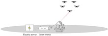
The purpose of this study is to solve the problem of shortening the endurance time of UAV clusters in rainfall environment by analyzing the attenuation characteristics of laser transmission and optimizing the energy distribution strategy. The focus is on quantifying the influence of rainfall intensity on laser energy transfer efficiency and UAV energy consumption, and developing a parameter adaptive charging strategy to extend the overall stagnation time. Therefore, the hovering energy consumption model of UAV is established, and the influence of raindrop kinetic energy on the energy consumption of UAV is included. The validity of the model is verified based on the experimental data of Inspire 2 four-rotor UAV. At the same time, the power budget model of laser wireless power transfer link is constructed based on Beer-Lambert law to characterize the attenuation law under light rain, moderate rain and heavy rain (5~25 mm/h). The model integrates the attenuation of laser transmission in rain, beam divergence, photoelectric conversion efficiency, communication energy consumption and subsystem loss, and more accurately calculates the received power of each UAV. An improved Spider Wasp Optimizer (SWO) algorithm is proposed. By introducing the Adaptive Moment Estimation optimizer (ADMA), the crossover probability of the SWO algorithm is dynamically adjusted through the gradient adaptive mechanism to improve the adaptability of the SWO algorithm to complex and dynamic environments. Enhance the overall robustness, adapt to different optimization stages, find a better balance between exploration and development, guide the update direction through gradient information, and improve the local search effect. On this basis, a meta-heuristic algorithm is proposed to calculate the influence of rainfall weather on laser transmission power in real time, which enhances the accuracy of the charging strategy. Combined with the working priority, charging efficiency and spatial position of the UAV, the reasonable allocation of energy is realized, the overall stagnation time is improved, and the landing rate is effectively reduced. Simulation experiments on 3-10 UAVs show that the proposed Adaptive Spider Wasp Optimizer Charging (AD-SWOC) strategy has significant advantages over FCFS and NJNP. Under 5 mm/h rainfall, AD-SWOC achieved a maximum increase of 31.34% in overall hover time, which was better than that of FCFS (22.1%) and NJNP (25.7%). In 25 mm/h rainfall, although the laser attenuation is serious, the average receiving power is reduced to 110 W, and the overall stagnation time can still be increased by 20.09%. The adaptive crossover probability mechanism makes the forced landing rate significantly lower than the fixed parameter method. When the UAVs reach 10, only 4 UAVs are forced to land, and the number of forced landings with fixed crossover probability is more than half of that of UAVs. The AD-SWOC strategy effectively alleviates the problem of UAV swarm endurance by systematically integrating rainfall-related laser attenuation analysis, adaptive optimization and multi-factor priority determination. The established model can accurately predict the laser power attenuation and UAV energy dynamics under different rainfall conditions, and support efficient energy management. By optimizing the charging scheduling based on real-time environment and task constraints, the strategy significantly prolongs the task duration and reduces the interruption caused by forced landing. This study provides a new theoretical and technical reference for the improvement of the stagnation ability of UAV swarms in other complex media. In the future, artificial intelligence technology can be introduced to predict more accurately according to meteorological conditions such as rainfall, air pressure and wind speed.
May. 25, 2025Vol. 54 Issue 5 0501003 (2025)
Tao XIANG, Bowei WANG, Ruitao YIN, Qi XIANG, and Hang ZHANG
Beam shaping is a crucial laser technology for achieving arbitrary light intensity distributions, typically achieved through Diffractive Optical Element (DOE). The Gerchberg-Saxton (GS) algorithm is an efficient method for DOE design, while problems such as local optima and poor uniformity remain unsolved. Therefore, improving the GS algorithm has become a research hotspot in diffractive optics. To increase diffraction efficiency and effectively suppress speckle noise, an improved GS algorithm based on feedback from non-signal region speckle is proposed in this paper. The core idea is as follows: first, the initial phase distribution is generated by using Zernike polynomial combined with polynomial weight coefficient Z. The weight coefficient Z is optimized through global amplitude constraint to determine the optimal Z value within a specific range, thereby resulting in an optimal initial phase form. Then, a basic target spot with high diffraction efficiency is obtained by GS algorithm, and the speckle feedback algorithm in non-signal region is used to suppress the speckle noise in non-signal region and improve the uniformity of signal region. In order to verify the effectiveness and generalization capability of the improved algorithm, the optimization designs were carried out for triangular spot, circular spot, and square spot, and the optical simulations and optical experiments were conducted. When shaping the Gaussian beam into a triangular spot under the constraint of RMSE<0.1%, the simulation results show that the diffraction efficiency of the improved algorithm reaches 98.30%, significantly higher than the87.49% achieved by the MRAF algorithm. The Root Mean Square Error (RMSE) is 0.27%, which is much lower than the 32.78% achieved by the GS algorithm. In addition, for circular and square spots, the results of the improved algorithm are also superior to the other two algorithms, demonstrating strong generalization ability for different spot shapes. The experimental results show that the improved algorithm has a speckle contrast of 0.020 9, while the GS algorithm has a speckle contrast of 0.280 1, which indicates that the improved algorithm has higher internal uniformity generation ability. Meanwhile, the Peak Background Ratio (PBR) is used to evaluate the speckle noise in the non-signal region. The PBR of the improved algorithm is 2.984 1, which is significantly higher than the 0.008 1 achieved by the MRAF algorithm, indicating that the improved algorithm has almost no speckle noise in the non-signal region, while the MRAF algorithm exhibits severe speckle. At the same time, this paper also discusses the influence of two key factors on the quality of the output light spot: 1) The influence of the waist radius on the output light spot. When the beam waist radius decreases to 600 μm, the overall brightness and uniformity of the spot are reduced, and pixel vortices are generated. However, when the waist diameter is expanded to 1 500 μm, the light spot generated by the improved algorithm can still maintain high diffraction efficiency and uniformity, which indicates that the improved GS algorithm exhibits certain robustness to different Gaussian beam waist radii. 2) The matching relationship between the beam waist and the position of DOE. Deviations from the optimal position significantly affect the output spot quality, leading to a decline in the quality of the spot. Three horizontal deviations of -0.32 mm, 0 mm and 0.32 mm are investigated in this paper, and the results show that these deviations can lead to a decrease in spot uniformity. In summary, when the Gaussian beam is shaped into the target spot, the improved algorithm not only improves the internal uniformity of the target spot, but also effectively inhibits the speckle noise in the non-signal region, while maintaining a high diffraction efficiency. The effectiveness of the improved algorithm is verified by optical experiments and simulations. The method proposed in this paper provides a valuable reference for designing DOE with high diffraction efficiency and uniformity.
May. 25, 2025Vol. 54 Issue 5 0505001 (2025)
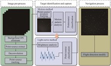
Kaiyu LEI, Hairui SANG, Xian SHI, Lin LI, Chunhui ZHAO, and Yanpeng WU
In the current deep space asteroid exploration missions, optical navigation is one of the main navigation systems, and autonomous target recognition is its highly critical part. Currently, motion analysis and light-curve analysis are two of the most widely used methods for autonomous target asteroid recognition. However, both of them are difficult to accurately identify the target within a short time (20 min). The traditional light-curve analysis method relies on the periodic brightness characteristics of asteroid. But in short-term observations, its brightness periodicity is not obvious, leading to the ineffectiveness of traditional methods, such as FFT and Lomb-Scargle, in distinguishing between stars and small celestial bodies.This paper focuses on the problem of autonomous target recognition in the autonomous optical navigation of the far-distant approach orbit phase in asteroid exploration missions and proposes a light-curve classifier based on Transformer, which can accurately distinguish between stars and small celestial body target from image of navigation camera within a short time (20 min).The Transformer-based classifier designed in this paper can extract both local and global features of the light-curve simultaneously. Its network structure retains only the encoder part of Transformer and adds linear layers and fully connected layers for the classification task. The encoder dynamically adjusts the weights through the multi-head self-attention mechanism to capture the periodic terms (local features) and trend terms (global features) in the input light-curves, thereby achieving the classification of stars and small celestial bodies.To train and test the classifier, this paper constructs simulation datasets and semi-simulation datasets. The simulation datasets are generated through computer graphics and photoelectric-link-simulation tools, simulating the light-curves of stallers and asteroid by star catalogue or target shape. The semi-simulation data integrates the DAMIT dataset and the MMT-9 dataset. Firstly, segmentation, fitting, and upsampling were performed on these light-curves to increase the sampling frequency, and short-time-interval and high-frequency simulation data were constructed using the photoelectric-link-simulation tool. The training strategy of the classifier adopts a pre-training and fine-tuning method: Firstly, pre-training is conducted using the simulation data, and then the classification layer is fine-tuned using the semi-simulation data.The classification results on the test dataset show that the proposed Transformer classifier achieves an average classification accuracy of over 95% on the simulation dataset, with a classification accuracy of 98.6% for stars and 95.4% for asteroid. On the in-orbit observation data of the OSIRIS-REx mission, compared with the Lomb-Scargle light-curve analysis and the motion analysis method, the Transformer classifier shows significant advantages. For the motion method, within a 20-min observation period, the positional changes of stars and target Bennu in the image are less than 5 pixels, making it difficult to distinguish and unable to complete the target recognition. Compared with the Lomb-Scargle algorithm, the Transformer classifier does not rely on the frequency domain features of the light-curve and can accurately distinguish between stars and non-star targets when lomb-scargle algorithm fail. Within a 20-min observation period, for the classification of target Bennu and background stars, the accuracy rates of the Transformer classifier are 92% and 83% respectively, much higher than 42% and 67% of the Lomb-Scargle algorithm.Based on the comprehensive experimental results, the proposed Transformer-based light-curve classifier exhibits excellent performance on both simulation and actual in-orbit data, effectively solving the problem of autonomous target recognition in the far-distant approaching orbit of small celestial body exploration missions within a short time. It significantly improves the accuracy of target recognition and provides an efficient technical approach for autonomous optical navigation in small celestial body exploration missions, possessing certain practical value and application potential.
May. 25, 2025Vol. 54 Issue 5 0510001 (2025)
Guodong YU, Jianguo ZHU, Chunyang WANG, Jianghai FENG, Xubin FENG, Shi LIU, Pengyu XU, Zhongqi LI, and Xiaochen LIU
As one of the key tools of damage assessment technology, infrared image is highly valued for its ability to provide reliable target information in various complex environments. However, due to the limited performance of the hardware equipment and the impact of the shooting environment, the infrared camera can not collect enough infrared image data to support the model training, which limits its effectiveness in practical applications. In contrast, the method of converting from visible to infrared images is becoming an alternative due to its low cost and ease of operation. Under the background of insufficient infrared data, this conversion method can effectively supplement the data source and support the damage assessment of military firing range. At present, the research on the deficiency of infrared data mainly focuses on the conversion from visible image to corresponding image. How to learn the mapping correlation between cross-modal data in the training process has become a key research problem that needs to be solved.In recent years, researchers have proposed a variety of cross-modal methods for converting visible light images to infrared images. By embedding the input visible image into the potential feature space, the corresponding infrared image is generated using the nonlinear transformation relationship. For example, the use of generative adversarial networks, unsupervised learning and self-supervised learning. However, the significant semantic gap between visible and infrared images remains a challenge. In order to effectively achieve cross-modal conversion, these methods often require additional constraints to ensure that the generated infrared image is not only close to realistic in appearance, but also able to retain key thermal characteristics. However, these methods show some limitations when dealing with the conversion task from visible light to infrared, because these methods are not designed for infrared images, they are difficult to achieve the expected effect when generating images that meet the infrared thermal characteristics. It is worth noting that the data collected in real scenarios is often unaligned, which increases the difficulty of cross-modal transitions.In order to solve the above problems, this paper proposes an infrared image generation method, Combining Generative Adversarial Network and Contrastive Learning for Infrared Image Generation (CLGAN), which combines generative adversarial network and contrast learning. Specifically, the method combines bidirectional contrast learning and feature mapping constraints to improve the quality of unpaired cross-mode conversion, effectively constrains cross-mode feature mapping, and ensures that the generated infrared image accurately reflects the thermal feature while retaining the visual feature. At the same time, the cross fusion self-attention is proposed to integrate local and remote associations adaptively with self-attention to realize efficient fusion of global information and ensure full utilization and comprehensive expression of feature information. In addition, the multi-scale feature refinement module is designed to further enhance the expression ability of key details and significantly improve the quality of the generated images through the refinement processing of multi-scale features. Extensive experimental results show that the proposed CLGAN outperforms existing methods in terms of both visual effects and performance indicators, generates clearer and more realistic infrared images, and has important potential in downstream tasks with limited infrared data.
May. 25, 2025Vol. 54 Issue 5 0510002 (2025)
Yun BAI, Junhong SU, and Kai SHI
For the optical components in the optical system, it is not only required to have good optical transmittance, but also to achieve the shielding of the electromagnetic wave band. Traditional metal materials suppress the light transmission performance while shielding electromagnetic waves. Carbon-based materials have become the first choice for mesh structure shielding materials due to their special physical and chemical properties and excellent electromagnetic shielding properties.In this paper, the copper metal plane structure is designed as a mesh structure, and a graphene layer is added to the copper mesh structure to establish a multi-layer copper-based graphene composite mesh structure model. In the range of 12~18 GHz electromagnetic frequency band, HFSS simulation software is used to simulate the electromagnetic shielding effectiveness of copper-based graphene multilayer composite mesh structure model by waveguide method. The linewidth parameters of the basic mesh structure are changed, and the electromagnetic shielding characteristics are simulated and experimentally studied. The absorption loss SEA and reflection loss SER of different structures are calculated to further explore the electromagnetic shielding mechanism of the new structure.The results show that in this electromagnetic frequency range, with the increase of electromagnetic wave test frequency, the electromagnetic shielding effectiveness SE of all structures shows a downward trend. When the same structure is at low frequency of electromagnetic wave, the shielding material has relatively poor permeability and propagation ability to electromagnetic wave, strong blocking ability to electromagnetic wave, and high electromagnetic shielding effectiveness SE. The electromagnetic shielding effectiveness of the three copper-based graphene multilayer composite mesh structures is improved compared to the single copper mesh structure. Among them, the double-sided superimposed graphene layer structure in the copper mesh structure is the best structure of the electromagnetic shielding effect in the three composite structures compared with the copper mesh structure. The relationship between the electromagnetic shielding effectiveness of the three composite structures is consistent with the theoretical calculation. The electromagnetic shielding effectiveness of this structure with double-sided graphene layer is more than 1.7 dB higher than that of a single copper mesh structure, and the absorption loss of electromagnetic wave is increased by 4.81 dB. Due to the superposition of graphene layers in the three composite structures, the absorption of electromagnetic waves by graphene is increased, so that the overall structure has a certain absorption effect on electromagnetic waves. While improving the overall electromagnetic shielding effectiveness of the structure, the composite structure also significantly improves the absorption loss of electromagnetic waves. Under the same electromagnetic frequency range, when the material properties of the composite structure and the mesh period are constant, the line width parameters of the basic mesh structure are changed. With the increase of the mesh line width, the electromagnetic shielding effectiveness of the composite structure is also increasing, while the mesh transmittance is decreasing. It is concluded that for the mesh substrate structure, there is a mutually restrictive relationship between electromagnetic shielding effectiveness and light transmittance.The electromagnetic shielding characteristics of three kinds of multi-layer composite structure samples designed by simulation are tested to verify the accuracy and feasibility of the simulation in this study. The experimental results show that the electromagnetic shielding effectiveness of the three multi-layer composite structure model samples is higher than that of the copper mesh structure model samples. The experimental results are almost consistent with the simulation and theoretical calculations, and the trend of the electromagnetic shielding effectiveness curve is consistent, which further verifies the feasibility of the simulation and the accuracy of the data results. The results of this study have certain reference value and reference significance for improving the electromagnetic shielding characteristics of metal materials and the electromagnetic shielding characteristics of metal and non-metal composite structures.
May. 25, 2025Vol. 54 Issue 5 0516001 (2025)
Ruixia MIAO, Jie YAN, Jiamei NIU, and Xiaotan JIA
β-Ga2O3 has a large band gap of 4.7~4.9 eV and a high critical electric field strength of 8 MV/cm. These properties allow β-Ga2O3 devices to operate at high power and strong radiation. In nuclear radiation environments, β-Ga2O3 devices will face significant challenges. The β-Ga2O3 material can generate many point defects in high-energy particle irradiation. The existence of strain field around the point defects, clusters with lower strain energy can be formed through migration and aggregation, and defects with more serious damage can be formed. However, the mechanism of irradiation defect migration in β-Ga2O3 materials has not been reported.The first principles calculation in this paper is based on density function theory, and the Perdew Burke Ernzerhof (PBE) functional under Generalized Gradient Approximation (GGA) is used to describe the exchange-correlation interaction of electrons. Considering that PBE method often underestimates the bandgap calculation, a hybrid functional HSE06 is used to introduce some Hartree-Fock interchange terms into the traditional GGA functional, which effectively improves the accuracy of bandgap calculation. The migration barrier of defects is calculated by the Climbing-Image Nudged Elastic Band (CI-NEB) method, which can accurately find the minimum energy path between the initial state and the final state and the corresponding transition state, which is helpful to further understand the migration behavior of defects.The results show that compared with Ga atoms, O atoms are more easily detached from lattice position to form VO and Oi. For VO defects, the migration barrier shows point-to-point dependence, and 23 possible migration paths are studied. The migration barrier of VO1 is the smallest in the 3 direction (migration barrier is0.48 eV). This low barrier indicates that VO1 can migrate spontaneously along this path at normal temperature. VO2 has the lowest migration barrier in the 11 direction (migration barrier is 0.015 eV) and almost no migration barrier, which means that VO2 has a very high migration activity at room temperature, which may significantly affect the electrical and optical properties of the material. The optimal migration path of VO3 is located in the direction of 18, and the corresponding migration barrier is 0.39 eV, which also has the possibility of migration at room temperature. In contrast, the migration barrier of VGa is relatively high, but there is still a relatively easy migration path: the optimal migration path of VGa1 is located in the 4 direction, and its migration barrier is 0.33 eV, which is slightly higher than the barrier of partial oxygen vacancy, but it is still possible to migrate under external excitation (such as irradiation, temperature increase, or electric field). VGa2 is also the easiest to migrate in the 4 directions with a corresponding barrier of 0.35 eV, indicating that its migration characteristics are similar to VGa1. The migration barrier of VO is generally lower than that of VGa, indicating that VO is more active in β-Ga2O3 crystals. Under irradiation or high temperature environment, the migration of VO may cause significant changes in material properties. According to the analysis of Oi migration path, the migration barrier corresponding to Oi2→Oi path is low (0.13 eV), which is significantly lower than the energy barrier of other Oi paths. It is shown that the Oi atoms are more inclined to migrate along this path in the crystal. In addition, due to the lower migration barrier, Oi2 path defects are more likely to accumulate or migrate under external excitation (such as irradiation). For Gai atom migration, Gai1→Gai6 is the optimal migration path, and the corresponding migration barrier is only 0.84 eV, which is much lower than other Gai migration paths. This low barrier value means that under certain conditions, Gai atoms have strong mobility, especially in the irradiation environment, and its dynamic behavior may have profound effects on the conductivity and stability of materials. The research results will help to further understand the microscopic mechanism of defect migration in β-Ga2O3 materials under irradiation and provide theoretical reference for irradiation reinforcement.
May. 25, 2025Vol. 54 Issue 5 0516002 (2025)
Yanjing LING, Bing XIE, Shuang ZHANG, Liping SUN, and Meng ZENG
Over the past decade, polariton condensate has attracted tremendous attention. In the semiconductor environment, the energy relaxation of polariton and the achievement of condensate are mediated by phonon relaxation. But this cooling mechanism is inefficiency, alternatively, the stimulated scattering mechanism of polariton condensate is studied in GaAs and CdTe, which is facing serious problems including the low saturation density and the small binding energy of exciton. As a result, ZnO, a wide bandgap material holds great promising for polariton condensate at room temperature, unfortunately, the stimulated scattering relaxation mechanism in ZnO has rarely been examined. Moreover, the occupancy in the ground state of polariton is crucial to trigger the stimulated scattering mechanism, but the evolution behavior of occupancy under different excitation powers has rarely been addressed by experiment in ZnO. In this paper, we report polariton condensate based on the stimulated scattering mechanism in ZnO at room temperature.Firstly, ZnO microwire is employed and fabricated via a carbonthermal method and characterized by scanning electron microscopy. Meanwhile, the radius size of cross section of microwire is considered to obtain polariton dispersion with proper energy range and effective mass. Then, to assess the strong coupling regime between photon and exciton in the sample, the dispersion of polariton is measured by using angle-resolved Photoluminescence (PL) spectroscopy technique with very weak excitation lasers and different polarization configurations at room temperature. After that, the experiment of power-dependence is carried out to obtain the evolvement of polariton dispersion. In addition, the evolvement of PL peak intensity, blueshift and linewidth in the ground state of polariton under different excitation powers are analyzed. Furthermore, the occupancy distribution along polariton dispersion for different excitation powers and the condensate fraction are studied. In the next step, the dynamical mechanism of polariton condensate is proposed according to the experimental data. In addition, the numerical simulation of Gross-Pitaevskii (GP) equation coupled with the Boltzmann rate equation to explain the dynamical mechanism of polariton condensate is performed to characterize the physical properties.The prepared ZnO microwire processes smooth facets and a regular hexagonal cross section, which can serve as Whispering Gallery (WG) optical resonator, in such quasi one-dimensional system the strong coupling between exciton and photon is obtained and the resultant Rabi splitting of polariton reaches 300 meV, demonstrating the robustness of the polariton in ZnO WG microcavity. The study of power-dependence measurement shows that the polariton condensate at room temperature is achieved and the threshold of condensate is 10 nW. At the same time, the exclusive PL emission from the ground state of polariton dispersion, the nonlinear increase of PL peak intensity, the rapid decrease of PL linewidth and the blueshift in the ground state of polariton are observed. It is noted that the maximum value of blueshift in the ground state of polariton is about 12 meV, which is 4% of the Rabi splitting, demonstrating that the photon and exciton remain in the strong coupling regime. The study of occupancy distribution along the dispersion with increasing excitation power shows that the occupancy distribution do not follow the ideal Bose-Einstein distribution function above threshold, indicating that there exists strong interaction between polariton, meanwhile the experimental condensate fraction is about 10%, because there exists strong interaction between polariton in condensate droplet, which is responsible for the depletion of condensate in ground state and thus in favor of the occupation in excited states above threshold. This can explain the obvious thermal cloud of noncondensated polariton under high excitation powers (such as 40 nW). Since the energy range and the effective mass of polariton dispersion exclude the phonon mediated relaxation mechanism during the condensate procedure, the polariton-polariton scattering relaxation is dominated and efficiency due to the large exciton oscillator strength in ZnO. The proposal that polartion condensate mechanism is based on polariton stimulated scattering is supported by the numerical simulation of GP equation, which is demonstrating the dynamical procedure of polariton condensate in ZnO WG microcavity at room temperature. The high energy state of polariton is served as a reservoir. Below threshold, the relaxation rate into the ground state from the reservoir is not able to overcome the radiation rate and the gain is not able to overcome the loss, then the occupancy is well below unity in the ground state and the polariton condensate does not occur. At threshold, the relaxation rate into the ground state balances the radiation rate and the occupancy in the ground state is unity and drives the stimulated scattering mechanism then the polariton condensate is achieved above threshold.In present study, by preparing processing unique properties, such as energy range and effective mass of polariton dispersion, polariton condensate based on the stimulated scattering in ZnO WG microcavity at room temperature is experimentally investigated successfully via angle-resolved PL spectroscopy technique by increasing the power of excitation laser, and the experimental condensate fraction is obtained. The direct occupancy distribution along the dispersion under different excitation powers is acquired, and the dynamics of polariton condensate driven by the stimulated scattering mechanism is well described by the GP equation coupled with the Boltzmann rate equation. The study shows that the dynamical mechanism of polariton condensate in ZnO WG microcavity at room temperature is stimulated scattering, we hope that our basic strategy and findings can be helpful on the design of quantum device based on the polariton condensate and on the understanding of the relationship between polariton-polariton scattering and quantum manipulation.
May. 25, 2025Vol. 54 Issue 5 0527001 (2025)
Fengxiang MA, Chen HANG, Xinyu ZHAO, Yajie ZHANG, Hongchao QI, Yue ZHAO, Feng ZHU, and Ke CHEN
Gas-insulation equipment is a key equipment for urban power grids and high-voltage power transmission. The chemical properties of SF6 gas are usually very stable, but when latent faults such as discharge or overheating occur inside the equipment, SF6 will decompose to produce toxic and corrosive gases such as SO2. SO2 indicates whether there is an arc or spark discharge fault in the equipment, and the SO2 content produced is closely related to the severity of the internal defects of the equipment. Electrochemical sensing, semiconductor sensing and gas chromatography are the main traditional methods for detecting SF6 decomposition products. However, they generally have disadvantages such as low sensitivity, large cross-interference, short life or long response time. Photoacoustic spectroscopy uses the sensed absorption energy to achieve gas detection and is a background-free and highly selective trace gas detection solution. SO2 gas has absorption in both mid-infrared and ultraviolet bands, ultraviolet Light-Emitting Diode (LED) has the characteristics of low cost, simple structure, low power consumption and good stability. Using photoacoustic spectroscopy and low-cost ultraviolet LED excitation source, a photoacoustic SO2 sensor with high sensitivity, high reliability and miniaturization for SF6 decomposition product in high-pressure gas insulation equipment is designed and implemented. An integrated photoacoustic SO2 sensor was designed, which mainly includes an excitation source, a lens group, a photoacoustic cell, a Micro-Electro-Mechanical System (MEMS) microphone, a gas pressure sensor, a window, an air inlet valve, an air outlet valve, an inlet and an outlet. The photoacoustic cell is a device for holding the gas to be measured, and the photoacoustic effect is generated here. The reasonable design of the photoacoustic cell structure is conducive to the improvement of the photoacoustic signal and the signal-to-noise ratio. The cell constant of the photoacoustic cell working in the non-resonance mode is inversely proportional to the square of the radius of the photoacoustic tube and the modulation frequency of the incident excitation light. The gas chamber volume and dimensions of the sensor are only 10.2 mL and 40 mm×40 mm×36 mm. This miniaturized design makes the sensor have the advantages of low gas consumption, simple structure and portability. Photoacoustic gas sensors are affected by gas pressure. The gas pressure range in the gas chamber of gas-insulation equipment is approximately 0.25~0.4 MPa. The photoacoustic signal is related to the degree of collision between the gas molecules to be measured. Theoretically, when the gas to be measured is in a state of non-saturated absorption and the gas concentration and the incident excitation power are constant, the high gas pressure will increase the energy absorbed by the gas molecules to be measured, thereby stimulating a stronger photoacoustic signal. Theoretical analysis and simulation verified the promoting effect of high pressure on photoacoustic excitation under SF6 background gas. The integrated pressure sensor is used to display the gas pressure value in real-time, and the influence of gas pressure on the photoacoustic response, background signal, noise and detection limit is tested. Real-time monitoring of SO2 concentration generated by SF6 decomposition to achieve accurate analysis and early warning of latent fault types and severity within gas-insulation equipment. Taking advantage of the positive correlation between photoacoustic excitation and gas pressure, the high sensitivity of the photoacoustic SO2 sensor in a high pressure environment is achieved. The performance of the photoacoustic SO2 sensor is tested under a gas pressure environment of 0.4 MPa. Detection limit is one of the most important factors in evaluating a sensing system. The results show that the detection limit reaches 56 ppb with an averaging time is 100 s, which provides a powerful preventive measure for the safe and stable operation of high-pressure gas insulation equipment.
May. 25, 2025Vol. 54 Issue 5 0530001 (2025)
Jing ZHANG, Yongkun WU, Xiuhua FU, Yonggang PAN, Zhaowen LIN, Fei YANG, Zhuobin HUANG, Guiqing WU, and Ben WANG
With the rapid development of optoelectronic detection technology, deep ultraviolet detection has been widely applied in various fields, including ultraviolet communication, missile warning, missile guidance, and discharge detection. The intensity of solar radiation near the ground within the 280~300 nm range increases exponentially with shorter wavelengths, and thus the response of ultraviolet detectors in visible and infrared wavelengths cannot be neglected. Although scholars at home and abroad have conducted some research on ultraviolet filters, there are few reports on deep cutoff filters with a center wavelength of 225 nm. Therefore, this paper describes the design and development of a deep cutoff filter utilizing a combination of metal and dielectric materials.First, we investigated the design theory of induced transmission filter and selected metal Al, UV-SiO2, Al2O3, and AlF3 as the film materials. By depositing single-layer of UV-SiO2, Al2O3, and AlF3, the optical constants of the three dielectric materials were obtained by using the whole spectrum fitting method. To obtain high-quality Al film, multiple experiments were conducted to separate boron nitride crucibles from copper crucibles, reducing thermal conductivity so that the Al film deposition rate climbed faster and more stably. Considering that Al film oxidizes when exposed to the atmosphere, a UV-SiO2/Al/UV-SiO2 symmetric film structure was designed and deposited. The ellipsometry parameters of this symmetric film structure were measured by using the ellipsometry method. By establishing an ellipsometry analysis model, the optical properties of the Al film were described using a general oscillators model combined with Tauc-Lorentz oscillators and Drude oscillator, allowing the optical constants of Al film be fitted and obtained. Based on the theory of induced transmission filter, a UV filter was designed using UV-SiO2 and Al, with an anti-reflection film designed on the back side using Al2O3 and AlF3. The final designed UV filter exhibited a peak transmittance of 33.21% at 225 nm, a half wave width of 28 nm, and an average cutoff depth of 4.7 OD from 280 nm to 1 200 nm. This design effectively collects UV signals, shields background interference caused by background spectral radiation during UV detection, and improves the accuracy of the UV detection system. Subsequently, a filter film sample was prepared based on the predetermined deposition process.Testing the spectral curve of the filter film sample revealed that the center wavelength of the test spectrum shifted towards the longer wavelength region compared to the design spectrum. After analyzing the influence of the metal layer on the spectrum and incorporating the tested spectral results, it was determine that the primary source of film thickness error lay in the dielectric layers. Then, we analyze the film thickness error through inverse fitting and investigate the reasons for the error in the dielectric layers. By increasing the crucible and allocating the film thickness reasonably, the prepared filter sample exhibited good consistency with the designed spectral curve, but there were still differences in peak transmittance and bandwidth. Considering that the rough surface of the thin film generates significant scattering losses in the ultraviolet band, atomic force microscopy was used to characterize the surface roughness of the filter. Furthermore, an equivalent absorption layer model was constructed, the optical constants of the equivalent absorption layer were calculated, and the influence of surface scattering on the spectrum was simulated. The findings indicated that the deviation in the spectral curve of the filter film was not only attributed to the random film thickness error in the film layers, but also related to the scattering loss caused by the rough surface of the film.An anti-reflective film was prepared on the back side, and the final prepared ultraviolet filter exhibited a peak transmittance of 31.55% at 225 nm, a half wave width of 28 nm, and an average cutoff depth of 4.4 OD between 280~1 200 nm. According to the GJB2485A-2019 general specification for optical film layers, the sample underwent the corresponding environmental tests, and after these tests, the surface of the film layer showed no defects such as peeling, delamination, cracks, bubbles, etc.Further research will focus on enhancing the transmittance of ultraviolet light and increasing the cutoff depth of background wavelengths.
May. 25, 2025Vol. 54 Issue 5 0531001 (2025)
Pengchong LIU, Donghui LI, Qi LI, Yuanheng ZHAO, Beilei WU, LIUYan, Jianyong ZHANG, Desheng CHEN, and Muguang WANG
In recent years, safety accidents have occurred frequently in our country, including the collapse of some large facilities, the leakage of oil and gas pipeline, the damage of railway track and so on. These occurrences underscore the imperative for enhanced safety monitoring methodologies to mitigate risks associated with major industrial accidents. Particularly for extended infrastructure networks and cross-regional pipeline systems characterized by vast spatial coverage, distributed monitoring solutions are necessary. Distributed optical fiber vibration sensing system has the advantages of simple structure, long detection distance, and electromagnetic interference resistance. Consequently, it has been widely applied in engineering fields such as earthquake monitoring, intrusion detection, pipeline monitoring.As a key technology in distributed optical fiber vibration sensing system, phase-sensitive Optical Time Domain Reflectometry (φ-OTDR) has the advantages of high sensitivity and fast response speed. The predominant phase demodulation technique employed in φ-OTDR systems capitalizes on the linear proportionality between phase variations in Rayleigh backscattering light and external perturbation intensity, enabling quantitative reconstruction of disturbance waveform. Because φ-OTDR uses highly coherent detection light, the Rayleigh backscattering light at different locations will interfere with each other. The photocurrent signal formed by the photodetector will produce strong fluctuation, resulting in an extremely low signal-to-noise ratio at some interference fading points. Therefore, it may produce false phase, which makes the system give false alarms and affects the accurate judgment of the system.As a method to suppress interference fading, the rotated-vector-sum method needs to be provided with vector components of different strength, and the vector signals are rotated in the same direction to sum, so as to maximize the strength of arbitrary vector addition. In past studies, academics have taken different ways to generate or utilize multi-frequency signals. In this paper, a new combination scheme of multi-frequency signals and rotated vector is proposed. It can use quasi-orthogonal chirped pulse and matching filter to provide vector components with different intensity. The components are rotated to the same direction and then added to improve the intensity. We also study the filtering effect of the matched filter, which can be expressed by cross-correlation value. The cross-correlation value of signals with opposite chirp polarity in non-matched filtering are discussed from three aspects: the relationship between band overlap rate and cross-correlation maximum, the relationship between signal bandwidth and cross-correlation maximum, and the overall cross-correlation value. The cross-correlation value of the quasi-orthogonal chirped pulse formed by the selected parameters is lower than that of the orthogonal code and special optical pulse code. It verifies the feasibility of using quasi-orthogonal chirped signal for distributed fiber sensing. Furthermore, we compared and analyzed the intensity fluctuation, interference fading probability and the phase curve. This scheme can reduce the intensity fluctuation of Rayleigh scattering curve by 20 dB, and the interference fading probability is reduced to 0.25%, which greatly reduces the false phase values and successfully inhibits interference fading. At the same time, the signal to noise ratio of demodulated vibration signal can reach 36 dB. The distributed fiber optic vibration sensing scheme can reduce the influence of interference fading, improve the precision of system positioning and the accuracy of disturbed signal recovery, and has high application value.
May. 25, 2025Vol. 54 Issue 5 0506001 (2025)
Ruiqi LI, Kang XIE, Yibin ZHU, Tingkuo CHEN, Han YANG, Qianfa LIN, and Hongyan XIA
Copper is a necessary trace element in the human body, with adults requiring about 2 mg per day. Functional materials containing Cu2? bring great convenience to life, but their released Cu2? from these materials are harmful to human health and the environment. Regulators have proposed allowable emission standards for copper (Ⅱ), among which “Drinking Water Sanitation Standard” (GB5749-2022) specifies 1.0 mg/L, with stricter standards in industrial emissions and sewage treatment plant pollutant discharge standards. The “Iron and Steel Industry Water Pollutant Discharge Standard” (GB13456-2012) sets 0.5 mg/L, while fishery requirements are the strictest under “Fishery Water Quality Standard of the People's Republic of China” (GB11607-89) limiting 0.01 mg/L. These regulations underscore the need for sensitive and selective detection of low concentrations of Cu2? for environmental, industrial, and human health applications.In this study, a tapered optical fiber sensor coated with CS-PVA composite coating is designed. The micro/nanostructure consists of a single-mode tapered optical fiber sensor whose tapered region generates evanescent waves. High-sensitivity detection of Cu2? in aqueous solution was achieved through coating a CS-PVA polymer composite film on the surface of the fiber's waist-cone region. Ion imprinting technology was applied to enhance the sensor, using glutaraldehyde as a crosslinker to strengthen the polymer network through the crosslinking agent, thereby enhancing metal ion adsorption. Regeneration using hydrochloric acid induces protonation of amine groups, creating repulsion between NH?? and adsorbed Cu2? for release.The ion-imprinted sensor demonstrated specificity when exposed to Cu2?, Cd2?, Fe3?, Co2?, and Pb2? confirming selective Cu2? detection. While the sensor primarily detects Cu2?, it could be adapted for other heavy metal ions through polymer template modification, showing great potential in heavy metal detection across environmental monitoring, industrial effluent testing and remote monitoring.Within 0~100 μmol/L Cu2?, the sensor reached 85.131 6 pm·μmol?1·L sensitivity with a limit of detection (LOD) of 0.388 μmol/L and linear response (R2=0.980 76). The improved ion-imprinted sensor exhibited specificity toward Cu2??. This easily fabricated sensor combines operational simplicity with high Cu2?? sensitivity while maintaining adaptability for other heavy metal ions through template ion substitution.The growing industrial demand underscores the importance of reliable Cu2?? detection for environmental and human health. We developed a simple, yet sensitive fiber-optic sensor for Cu2??. Three sensor configurations were fabricated via dip-coating: uncoated, CS-PVA-coated, and CS-PVA ion-imprinted variants. Experimental results demonstrate that, within 0~100 μmol/L Cu2?? concentrations, the CS-PVA-coated sensor achieved 85.131 6 pm·μmol?1·L sensitivity, an LOD of 0.388 μmol/L, and linear response (R2=0.980 76). The improved ion-imprinted sensor showed specificity toward Cu2?. Combining ease of fabrication with operational simplicity, this platform enables specific Cu2? detection while remaining adaptable for other heavy metal ions through imprinting modifications.
May. 25, 2025Vol. 54 Issue 5 0506002 (2025)
Zhijun WANG, Shengyou HUANG, Kun LI, Yang YANG, Fudan CHEN, Binbin LUO, Decao WU, and Xue ZOU
The vocal cords serve as the primary organ responsible for human vocalization. The vibrational signals generated by the vocal cords carry abundant textual information, much like those of speech signals. Vocal cord vibration recognition technology has the potential to effectively address the fundamental communication challenges encountered in the daily lives of individuals with language disorders. The utilization of flexible pressure sensors enables the detection of vocal cord vibrations and facilitates the discrimination of subtle variations within these vibrations. However, traditional electrical sensors are plagued by issues such as parasitic effects and electromagnetic interference, which significantly restrict their practical application in the detection of vocal cord vibration signals. In contrast, fiber optic sensors, particularly Micro-Nano Fiber (MNF) sensors, are more apt for detecting vocal cord vibrations owing to their small size, rapid response speed, and high sensitivity.At present, some researchers are engaged in using MNF for vocal cord recognition studies, although the intelligent classification and recognition of vibration signals as corresponding speech information has not yet been accomplished. Integrating wearable devices with deep learning presents a novel approach to accurately recognizing vocal cord vibration signals. This paper designs and fabricates a wearable flexible sensor featuring an S-shaped MNF, which consists of two layers of polydimethylsiloxane (PDMS) films with an S-shaped bent MNF embedded within it. The S-shaped MNF structure enlarges the contact area between the optical fiber and the vocal cords, thereby augmenting the efficiency and sensitivity of vocal cord vibration signal acquisition, enabling the capture of more stable and accurate signals. Additionally, this design makes the optical fiber's mode field more susceptible to vocal cord vibrations. When the vocal cords vibrate, the curved sections of the S-shaped structure experience minute displacements and deformations. These changes lead to substantial variations in the phase and intensity of the optical signals within the S-shaped MNF, which contain characteristic information regarding the vocal cord vibrations. Furthermore, combining the S-shaped MNF with flexible PDMS material effectively prevents local pressure or damage to the vocal cords during use, thus enhancing the safety and repeatability of the sensor. Subsequent in-depth simulation studies disclose that the evanescent field of the MNF increases as the MNF diameter and bending radius decrease. To balance the strength of the optical fiber with the contact area, the optimal sensor parameters were ultimately determined, specifically an MNF diameter of 4 μm and a bending radius of 1 mm.In terms of performance evaluation, this article has comprehensively investigated the response of MNF flexible sensors to both static and dynamic pressure as well as vibration. Experimental results show that the sensor's response time (222 ms) and recovery time (163 ms) are both under 300 ms, thereby demonstrating its rapid responsiveness to external stimuli and excellent durability. Across different frequencies, the sensor displays significant response variations at each test frequency, indicating strong frequency adaptability. In vocal cord vibration recognition, the sensor is worn in the vocal cord region of the human body. When the subject utters a sound, the vibrations of the vocal cords lead to changes in the transmitted light intensity of the sensor. A photodetector (PD, CONOUER, 200 kHz) converts the light intensity into corresponding electrical signals in real-time, and these signals are then transmitted to an oscilloscope for display and monitoring. The subject is required to repeatedly pronounce the 26 English letters, facilitating the acquisition of precise light-intensity spectral responses. A total of 1 660 datasets are obtained and combined with the target detection algorithm (YOLOv8) for the classification and recognition of vocal cord vibration signals, achieving an average recognition accuracy of 96.8%. To further assess the sensor's universality, vocal cord vibration data for four commonly used high-frequency phrases—“Ni Hao”, “Zao Shang Hao”, “Hello”, and “How Are You”—were collected from ten participants (5 males, 5 females). The YOLOv8 model was used to train and recognize 1 200 collected datasets. Among these phrases, the recognition accuracy for “How Are You” was the highest at 99%, with an average recognition accuracy across all phrases being 97.75%. These results suggest that the sensor attains high recognition accuracy across multiple individuals, highlighting its strong generalization capability. To comprehensively showcase the advantages of the proposed flexible wearable sensor based on MNF combined with deep learning technology, a detailed comparison was carried out with other sensors paired with different deep learning models regarding accuracy. The results disclose that the S-shaped MNF sensor combined with the YOLOv8 model used in this study achieves high accuracy in recognizing various characteristic signals (26 English letters). Moreover, even with 10 test subjects, the model maintains outstanding accuracy in identifying four commonly used phrases. Therefore, the proposed approach not only surpasses other methods in terms of accuracy but also exhibits significant advantages in meeting diverse requirements and demonstrating broad applicability.This study designs and fabricates a flexible wearable sensor that is based on a PDMS-encapsulated S-shaped MNF structure for the recognition of vocal cord vibration signals. Through theoretical modeling, simulation, and analysis, the main structural parameters of the sensor are rationally designed in order to achieve high sensitivity, reliability, and applicability. By utilizing the YOLOv8 deep learning model, the sensor successfully recognizes 26 English letters with an accuracy rate of 96.8%, thereby demonstrating its significant potential in vocal cord vibration recognition applications. To further enhance the generalizability of vocal cord vibration recognition, training is carried out using the pronunciations of four commonly used words from 10 different subjects, attaining a recognition accuracy of 97.75%. This effectively validates the sensor's universality and reliability among different users. The sensor is simple to fabricate, highly reliable, and possesses excellent resistance to electromagnetic interference, thus offering promising prospects in human-computer interaction applications. Future work will concentrate on testing across diverse populations and system optimization to establish a cloud database, further expanding its application potential in vocal cord vibration recognition, and holding prospects for assisting individuals with speech disabilities in daily communication.
May. 25, 2025Vol. 54 Issue 5 0506003 (2025)
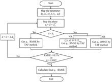
Shiyu ZHAO, and Fen GAO
Point diffraction interferometry is a method for the detection of super-precision surface shape of optical components. This method uses micron-scale hole diffraction to generate nearly ideal spherical wave as the reference surface, which gets rid of the reference mirror's limitation on the accuracy of traditional interferometry. If the interference technology based on point diffraction can be extended to the field of three-dimensional measurement, it will be expected to provide a new way for ultra-high precision three-dimensional measurement. In order to solve the problem of non-destructive measurement of three-dimensional topography of complex curved surfaces in small areas, a three-dimensional topography measurement method based on point diffraction interference technology is proposed. The high-precision point diffraction interference fringes are generated by double optical fibers, and the fringes are projected on the surface of the measured object. The piezoelectric ceramic phase shifter drives the mirror to generate phase shift, and seven interference images with different phase shift are obtained on the CCD detector. By collecting and processing the deformed interference fringes modulated by the height information of the measured object, the three-dimensional topography information of the measured object is recovered. A specific three-dimensional measurement optical path scheme of point diffraction interference fringe projection based on phase-shifting of double fiber splitting path is proposed, and the phase-height recovery mathematical model of the measurement system is constructed. Based on the simulation of seven-step phase-shifting projection interference fringes, the interference image processing algorithm is studied, which mainly includes interference image preprocessing, edge detection, edge extraction, phase extraction, branch-cut phase unwrapping and phase-height information restoration based on the continuous phase information distribution obtained by unwrapping. The system structure parameters are calibrated. According to the relationship between the pixel coordinates of the camera image and the world coordinates, Zhang Zhengyou camera calibration is used to calibrate the camera parameters. Based on the lens imaging principle and the mathematical relationship of the projection system, the specific calibration algorithm formula is derived. By using the electronically controlled displacement table and the corner detection method, the distance from the optical center of the camera lens to the reference plane and the central projection angleof the optical fiber projection end are calibrated respectively. Based on an optical fiber with a core diameter of 4 μm and a core distance of 120 μm, an actual point diffraction interference three-dimensional topography measurement experimental system was built. The three-dimensional topography of a hemispherical plaster model with a diameter of about 40 mm was measured six times repeatedly. The average height of the center of the measured object is 19.280 1 mm. Finally, to verify the feasibility and correctness of the proposed method, the measurement results of the system are compared with those of the ATOS Compact Scan commercial three-dimensional scanner of GOM company in Germany. The experimental results show that the difference between the arithmetic mean value of the center height of the two measurement methods is only 0.000 2 mm, which verifies the correctness and reliability of the experimental system. The standard deviation of the center height measurement results of the point diffraction interference three-dimensional topography measurement system is 0.001 3 mm, which verifies that the experimental system is feasible and stable. The proposed system integrates point diffraction interferometry with three-dimensional measurement technology, offering advantages such as high precision and non-destructive measurement, while featuring a simple principle and ease of implementation. The research results effectively realize high-precision three-dimensional shape measurement, which can provide theoretical reference for the extended application of point diffraction interference technology in the field of three-dimensional shape measurement.
May. 25, 2025Vol. 54 Issue 5 0512001 (2025)
Zeyu ZHENG, Chao YE, Yucong ZHOU, Chunlian ZHAN, and Han GAO
Polarization detection technology plays an important role in fields such as environmental exploration, remote sensing imaging, materials science, biomedical applications, and aerospace. Compared with traditional light intensity and spectral detection technologies, polarization detection can provide information about the target's material, refractive index, surface normal direction, etc., significantly improving the capability of obtaining and analyzing target information. However, traditional polarization detection systems are large in size, slow in detection, and difficult to meet the requirements for miniaturization, light weight, and rapid detection. In recent years, the development of metasurface technology has brought new opportunities for polarization detection. Metasurface devices can flexibly control the phase, amplitude, and polarization of light, providing effective solutions for miniaturized and lightweight polarization detection devices. In recent years, the Metagrating designed by Capasso team which achieves full-Stokes vector polarization detection and imaging by separate or control polarization information in the same region, making the device smaller and easier to integrate. Furthermore, by applying Fourier optical theory, the Metagrating achieves precise optimization of the size of each nanocolumn, avoiding cross-interference and losses caused by light field coupling between multiple regions, thus providing high polarization detection energy efficiency. However, due to factors such as processing precision and system integration errors, there is a deviation between the theoretical and actual instrument matrix value of the Metagrating, leading to the decrease of polarization detection accuracy. Therefore, the instrument matrix must be calibrated before polarization detection. The commonly used calibration method (two-step method) for the instrument matrix contains linearly polarized light and circularly polarized light calibration, respectively. The calibration procedure is cumbersome and time-consuming. Additionally, the calibration accuracy is also affected by the imperfect circularly polarized light in lab condition. Accumulated errors from multiple calibration experiments will further reduce the accuracy of polarization detection. To address the disadvantages of traditional instrument matrix calibration methods, this paper proposes a “one-step” calibration method based on elliptical polarized light, which only requires one experiment and avoids errors caused by imperfect circularly polarized light, effectively simplifying the calibration process and avoiding the accumulation of measurement errors.This paper uses a two-dimensional Metagrating with four independent polarization analysis channels (order (1, 0), order (-1, 0), order (0, 1) and order (0, -1)). When light with any polarization state is incident on the Metagrating, diffraction light with specific polarization is generated in the four polarization analysis channels. This modulation process is represented. During polarization detection, four light intensities from the polarization analysis channels can be simultaneously obtained by the detector. If the instrument matrix A is known, the Stokes vector of the incident light can be determined, achieving polarization detection. This process is expressed, where the instrument matrix A of the Metagrating is a 4×4 matrix. When use two-step method to calibrate linear polarization component, S4=0, so the fourth column circular polarization component of the instrument matrix cannot be calibrated. However, if all four parameters of the Stokes vector are non-zero and their values change with the incident polarization angle, the four parameters of the instrument matrix can be calibrated simultaneously in a single experiment. Considering the four Stokes parameters of elliptical polarized light are non-zero, we propose a one-step calibration method based on elliptical polarized light to simplify the calibration process.Experiments comparing the effects of the “one-step” method and the “two-step” method on the polarization detection accuracy of 1 550 nm two-dimensional Metagrating are shown in Figures 3 to 5. As shown in Table 1, it can be seen that, although the Root Mean Square Error (RMSE) for Degree of Polarization (DOP) of linearly polarized light using the “one-step” method is slightly higher than that of the “two-step” method, the magnitude is the same. The RMSE for the Angle of Polarization (AOP) increases by less than 1°, with only a 0.45% decrease in accuracy. In elliptical polarized light detection, the RMSE values for AOP, Ellipticity of Polarization (EOP), and DOP using the “one-step” method decrease by more than 2.5°, 2.0°, and 0.016, respectively, improving the detection accuracy by 3.05%, 2.76%, and 1.65%. In partial polarization DOP detection, the RMSE for the “one-step” method is also smaller, with accuracy improving by 0.51%. To validate the robustness of the “one-step” calibration approach across different experimental platforms, we performed analogous experiments using a 500 nm Metagrating. It shows similar trends to the 1 550 nm experimental results. This method significantly improves the detection accuracy of elliptical polarized light and partial polarized light, with the RMSE for AOP, EOP, and DOP decreasing by 2.902°, 1.883°, and 0.020, respectively, and detection accuracy improving by 2.66%, 2.16%, and 2.08%. The above results demonstrate that the “one-step” method effectively simplifies the instrument calibration steps before polarization detection, significantly improving the accuracy of polarization Metagrating detection, and provides a new technical approach for constructing high-precision, fast polarization detection systems.
May. 25, 2025Vol. 54 Issue 5 0512002 (2025)
Zihao ZHANG, Jiangpei DOU, Yaya MAO, Jing GUO, Gang WANG, and Yongtian ZHU
Direct imaging of exoplanets is able to measure planetary mass, orbital parameters and other critical physical information, which can support investigations into the potential processes behind the formation and evolution of both solar and extrasolar planetary systems. However, due to the significant brightness contrast ratio between exoplanets and their host stars, as well as limitations imposed by telescope apertures, the faint planetary signals are often obscured by the diffraction light from thire host star. Furthermore, many current and planned large-aperture astronomical telescopes adopt segmented mirror structures, the gaps between adjacent mirror segments will lead to considerable additional diffraction, thus it poses even greater challenges to the direct imaging studies of exoplanets.To address this issue, a high-contrast imaging coronagraph system based on pupil phase modulation by using a large-actuator-number and high stability Spatial Light Modulator (SLM) is proposed in this paper. The system aims to achieve high-contrast imaging capability across the 360° full-field region for telescopes with a monolithic mirror and large-aperture segmented mirrors. The Stochastic Parallel Gradient Descent (SPGD) optimization algorithm is employed to control the SLM for pupil phase optimization, and the contrast performance is evaluated using an objective function defined from the Point Spread Function (PSF) images collected by a CCD. Firstly, the fundamental principles of pupil phase modulation and the SPGD algorithm are introduced, theoretically demonstrating the feasibility of using SPGD to control the SLM for optimizing the pupil phase distribution to achieve high-contrast dark zones. Based on practical observation targets, the inner and outer working angles of the coronagraph system are defined as four times the working wavelength divided by the telescope aperture and twelve times the working wavelength divided by the telescope aperture, respectively, which further determines the evaluation function of the optimization algorithm. Secondly, an optimization testing system for a phase modulation-based coronagraph is constructed, in which a phase-type SLM is used to modulate the pupil plane phase, moreover, an amplitude-type SLM is used to simulate the pupil structure of large astronomical telescopes, enabling optimized design and experimental tests for both monolithic and segmented-mirror telescopes with ten meters aperture or larger. In the experiment, to fully leverage the advantage of the large number of actuators on the SLM and ensure rapid convergence of the SPGD algorithm for optimal imaging contrast performance, a finite-band ring-based pupil phase modulation method is designed. This method distributes a finite number of equally wide concentric rings from the center of the pupil along the radial direction, assigning the same phase value to each ring to reduce phase precision while maintaining final imaging contrast performance, and the modulated pupil area matches or slightly exceeds the simulated telescope pupil to maintain modulation effectiveness. Voltages of actuators in each ring within the SLM's optimization region are controlled by using an SPGD optimization algorithm that adjusts the pupil phase values according to the values of the objective function to improve contrast performance. The optimal imaging contrast on the focal plane in the experiment is eventually achieved when the objective function's value no longer decreases and reaches the minimum. Optimization tests are conducted for simulated monolithic and segmented-mirror telescopes individually by using an amplitude-modulated SLM to simulate the pupil of each configuration. PSF images before and after modulation are compared and significant modulation effects can be observed. The final optimized pupil distribution is acquired, and the imaging contrast curve is measured using the triple-exposure method developed by our group. To eliminate uncertainties caused by curve-fitting errors in the contrast measurement, an additional laser source was used to simulate a planetary light source for further verification of the system's imaging contrast. Finally, we conduct an analysis and discussion based on the results. The experimental results show that the proposed high-contrast imaging system achieved an imaging contrast of approximately 3.6×10⁻⁶ after 5 000 iterations for a simulated monolithic mirror telescope, while for the simulated large-aperture telescope with segmented mirrors, an imaging contrast of approximately 9.3×10⁻⁶ was achieved after 9 400 iterations of optimization. By comparing the two outcomes of the imaging contrast, it indicates that the complex additional diffraction caused by the gaps between adjacent segments in a large-aperture telescope with segmented mirrors sacrifices a portion of the coronagraph system's imaging contrast performance, posing challenges for high-contrast imaging in coronagraph systems and needs to be carefully tackled.In conclusion, the proposed high-contrast imaging coronagraph system based on a phase-modulation SLM achieved an imaging contrast better than 10-5 within the 360° full-field range of 4λ/D to 12λ/D from the PSF center in optimization tests simulating both monolithic and large-aperture telescopes with segmented mirrors. The proposed phase-modulation coronagraph system shows potential for direct imaging of exoplanets.
May. 25, 2025Vol. 54 Issue 5 0522001 (2025)
Qiancheng YU, Xu LIU, Lin MA, Jinhua WU, and Zuyuan HE
With the rapid advancements in technologies like 5G, big data, and AI, Internet data traffic is rising exponentially, driving an urgent need for high-speed data interconnects in data centers. Large-scale models such as ChatGPT require robust interconnect systems to facilitate high-capacity chip communication. However, traditional electrical interconnects face limitations, including signal loss, power consumption, and reliability issues, particularly for centimeter- to meter-scale board-level distances. Optical interconnects, with their high bandwidth, fast data rates, low power needs, and immunity to electromagnetic interference, are increasingly preferred for next-generation systems.Polymer waveguides, compatible with both Printed Circuit Boards (PCBs) and optical fibers, support high-density, high-speed connections with low propagation loss. Polymer-based optical backplanes currently reach transmission rates of up to 112 Gbps per channel. To increase capacity further and achieve transfer rates of 400 Gbps, 800 Gbps, and up to 1.6 Tbps, Wavelength Division Multiplexing (WDM) is a promising technology, especially in the O-band (1 260~1 360 nm). Among WDM options, Coarse Wavelength Division Multiplexing (CWDM) offers cost benefits in equipment and maintenance. CWDM systems rely on (de)multiplexers(MUX) for separating and combining different wavelengths. Common (De)MUX designs include arrayed waveguide gratings, planar concave gratings, and microring resonators. The cascaded Mach-Zehnder Interferometer (MZI), due to its low insertion loss, wide bandwidth, and low crosstalk, is widely used for CWDM devices. While CWDM research is extensive, studies on polymer-based devices remain limited. Polymer waveguides exhibit lower refractive index contrast and larger feature sizes, providing reduced sensitivity to geometric variations and allowing larger fabrication tolerances. Polymer waveguides are also straightforward to manufacture through spin-coating and UV lithography at room temperature, which helps minimize costs. With polymer waveguides validated for high-speed interconnect backplanes, CWDM integration can enable cost-effective all-polymer optical circuit boards with enhanced communication capacity and data rates. This work presents a four-channel CWDM device based on a two-stage cascaded MZI structure in polymer waveguides. The MZI design uses Multimode Interference (MMI) couplers as power splitters, which are insensitive to wavelength and polarization, contributing to stable performance. By optimizing the MMI′s parameters, we achieved consistent performance, with insertion loss and imbalance variations kept within 0.1 dB and 0.4 dB, respectively, even with a 10% variation in refractive index contrast. This improves the device′s resilience to refractive index changes from temperature fluctuations. To further reduce insertion loss in phase arms, we introduced an offset at the junction between curved and straight waveguides, achieving a device loss reduction of approximately 1.5 dB. Simulations and experimental results demonstrate that the device achieves an insertion loss below 3 dB in the O-band, with crosstalk below -28 dB across a 3-dB bandwidth. Experimental verification, achieved through UV lithography, confirmed an excess insertion loss of 2.7 dB in the O-band, a 3-dB bandwidth of 20 nm, and channel crosstalk consistently under -20 dB. The device′s polarization-dependent loss remains below 1 dB. Thermal stability tests indicate a spectral shift of less than 1.8 nm at 150 ℃, suggesting suitability for high-speed board-level optical interconnects where operating temperatures can vary. In conclusion, this study presents the design and fabrication of a polymer-based four-channel CWDM device with a two-stage cascaded MZI structure, optimized for low insertion loss, wide bandwidth, and low crosstalk. This CWDM solution holds potential for scalable optical interconnects in data centers, offering a practical pathway toward low-cost, high-speed all-polymer optical circuit boards.
May. 25, 2025Vol. 54 Issue 5 0523001 (2025)
Luanxuan HE, Ping CHEN, Jie LI, Hulin LIU, Jinshou TIAN, Wenbo HU, and Shengli WU
This paper focuses on addressing the challenges of low gain and poor gain uniformity in side-window dynode photomultiplier tubes (PMTs). Using CST software for simulation, the study proposes an optimization approach based on three-dimensional dynamic simulation technology. By constructing a highly accurate simulation model, the influence of multiple structural parameters-including photocathode position, dynode shape, arrangement angle, spacing, and length-on the gain performance of the PMT is systematically analyzed. Furthermore, visualized electron trajectory tracking technology is utilized to intuitively demonstrate the effects of different structural configurations on electron motion paths and gain behavior.The side-window PMT model developed in CST retains the core components critical to gain performance, including the grid mesh, cathode, nine-stage dynodes, and anode. The surfaces of the dynodes are coated with high secondary electron emission materials, which emit secondary electrons under bombardment by incident electrons. The entire model operates in a vacuum environment. In the simulation, photoelectrons emitted from the cathode under the influence of an electric field strike the dynode surfaces, exciting secondary electrons. These secondary electrons, driven by the electric field gradient, repeatedly collide between the dynodes and undergo successive multiplication, eventually reaching the anode, where they are absorbed to generate an output electrical signal. The proposed simulation approach has been validated through the design and development of several PMTs, confirming its reliability. Previous applications of this method have successfully contributed to the design of other types of PMTs that have been implemented in practical production.The study shows that optimizing the relative angle between the photocathode and dynodes improves electron collection efficiency, increasing it to 77%. Modifying the dynode shape (e.g., optimizing it to an arc shape) and adjusting its curvature can further focus the electron trajectories, significantly enhancing dynode gain performance. Additionally, optimizing the spacing and length ratio of the dynodes is critical to improving overall gain: when the spacing is set to 7.5 mm, the gain reaches its maximum; when the length ratio of the dynode to cathode is optimized to 1.4, gain loss is minimized. Through these structural optimizations, the PMT gain increases from an original value of 9.1×10⁶ to 2.1×10⁷ without altering the dynode material or operating voltage.In summary, the study demonstrates that in the design of side-window PMTs, adjusting the angle between the grid mesh and the photocathode, as well as modifying the electric field distribution among the cathode, grid mesh, and dynodes, can more effectively guide photoelectrons emitted from the cathode to be collected by the dynodes, thereby enhancing the overall gain of the PMT. The variation in dynode shape leads to differences in the electric field distribution between dynodes, which subsequently affects the trajectories of secondary electrons emitted by the dynodes. Arc-shaped dynodes, in particular, are shown to have the potential to partially focus electron trajectories. By adjusting the curvature of the arcs, the positions at which secondary electrons bombard the next-stage dynodes can be altered, enhancing the electron collection efficiency of the dynodes and effectively increasing the PMT gain.For cage-structured dynode arrangements, when the shape and voltage distribution of the dynodes are fixed, there exists an optimal spacing between dynodes. This optimal spacing arises due to changes in the electric field intensity between the dynodes, which influence the impact positions of the electrons on subsequent dynodes. Additionally, photoelectrons emitted from the edges of the cathode are less likely to be collected by the dynodes. Optimizing the length ratio between the cathode and dynodes is shown to improve the cathode's sensitivity and the overall gain of the PMT.In conclusion, the proposed simulation and optimization methods provide a systematic framework for improving the design and performance of side-window PMTs. The significant gain improvements achieved through these optimizations underscore the potential for broader application of these design principles in the development of next-generation photomultiplier tubes.
May. 25, 2025Vol. 54 Issue 5 0523002 (2025)
Chongzhou LI, Peiyao WANG, Mingquan LONG, Yufeng XU, Ruozhong HAN, and Tianqing JIA
ITO thin films have excellent electrical properties, with low resistivity and high carrier concentration, showing metal-like properties. ITO films also have excellent optical properties, with high transmittance to visible light, high reflectivity to infrared light and high absorption rate to ultraviolet light. In addition, ITO films have high degeneracy, good physical and chemical stability, and good adhesion to the substrate. ITO films have been well applied in the field of flat panel displays such as liquid crystal display and touch screen, and in the field of optoelectronic devices such as light-emitting diodes and solar cells.Compared with nanosecond laser, femtosecond laser processes materials with smaller thermal effects. The ablation efficiency of femtosecond laser with lower laser fluence is lower. Improving the laser fluence of femtosecond laser can effectively improve the processing efficiency, but also reduce the processing quality. Using femtosecond laser pulse train can improve the processing efficiency and ensure good processing quality. After the first pulse interacts with the material, the second pulse interacts with the molten ejecta formed by the first pulse, which can effectively reduce the size of the ejected particles. At present, the mainstream methods of generating pulse train are complicated in principle and equipment, poor in stability, and difficult to change sub-pulse interval, such as Michelson-like interferometer. The pulse train generator based on Fabry-Perot (F-P) cavity is simple, low-cost and flexible in sub-pulse interval variation. In this paper, we use pulse trains generated by F-P cavity to process ITO films with a thickness of 185 nm, and the sub-pulse interval can vary within the range of 1~1 500 ps. High-quality etched lines and complex wires were processed on ITO films.A high-quality etched line needs to have the following characteristics. First, the film is completely etched through. Second, the line width is narrow. Third, the line edge roughness is small. Fourth, the angle between the side wall and the sample surface should be close to 90 degrees. Fifth, the degree of protrusion on the line edge is small. Sixth, the etched volume of bottom glass is small. When comparing the appearance of two etched lines, we also take the above six aspects as evaluation criteria. Firstly, we study the etched lines processed by the original Gaussian light. We constantly change the laser fluence and scanning speed, and explore the change of the evaluation criteria of the etched line under different laser fluence and scanning speed. Secondly, we compare the overall appearance of etched lines processed by pulse train and Gaussian light under various parameters, and find that the edge roughness of etched lines processed by the pulse train is much lower than that processed by Gaussian light, which is also the core innovation point of this paper. Finally, we study the etched lines processed by pulse train. We constantly change the laser fluence and scanning speed, explore the change of the evaluation criteria of etched lines under different sub-pulse intervals, laser fluence and scanning speed, and find a set of optimal parameters for processing etched lines. High-quality etched lines were fabricated when the sub-pulse interval is 150 ps, the laser fluence is 0.49 J/cm2, and the scanning speed is 0.2 mm/s. The line width is only 1.45 μm at the top and 0.95 μm at the bottom, and the line edge roughness is only 9.48 nm.After obtaining the optimal parameters for processing etched lines, we explore the influence of the interval between two adjacent etched lines on the appearance of etched lines. We keep changing the distance between two adjacent etched lines and observe the change of the overall appearance of etched lines. According to a large number of experimental results, we believe that when using this particular set of optimal parameters, and when the center distance of two adjacent etched lines is more than 2 μm, the appearance of an etched line is basically not affected by other etched lines, and processing multiple etched lines can be regarded as a simple repetition of processing an etched line. According to the above experiment, we processed complex wires with smooth edges and uniform width of only 2 μm.In summary, the appearance of the etched lines processed by pulse train is better than that processed by Gaussian light, especially the line edge roughness is significantly improved. Femtosecond laser pulse train can take both processing accuracy and processing efficiency into account, suitable for precise processing. Laser pulse shaping is expected to overcome the problems of thermal effect and insufficient energy deposition during femtosecond laser processing, reduce the size of ejected particles and improve the processing efficiency and accuracy.
May. 25, 2025Vol. 54 Issue 5 0532001 (2025)
Sen ZHAO, Yongsheng GOU, Yang YANG, Zhen CHEN, Bo WANG, Penghui FENG, Yan XU, Jinshou TIAN, and Baiyu LIU
Inertial Confinement Fusion (ICF), a leading approach for controlled nuclear fusion, has garnered considerable attention due to its potential for sustainable energy production. ICF experiments involve the implosion of a target capsule driven by high-power laser pulses to create extreme temperature and pressure conditions necessary for fusion. During this process, X-ray radiation emitted by the plasma carries critical spatiotemporal information, which is crucial for understanding and optimizing the fusion dynamics. To capture the fine details of this ultra-fast process, X-ray framing cameras with ultra-high temporal and spatial resolution are employed.However, current X-ray imaging techniques face stringent requirements regarding time synchronization accuracy and trigger jitter, which can severely affect the precision of image capture. The frame rates of ultra-fast digital framing cameras have already reached the picosecond (ps) scale, and timing errors, such as nanosecond- or even picosecond-level trigger jitter and delay, can significantly compromise the quality of the images. Therefore, developing a synchronization system that ensures high precision and low jitter is pivotal for achieving accurate imaging in ICF experiments.Traditional synchronization methods for measuring and compensating trigger jitter include the current integration method and FPGA-based carry-chain techniques. The current integration method, theoretically capable of providing high measurement precision, suffers from considerable measurement errors due to temperature fluctuations, electromagnetic interference, and noise, which undermine its reliability in ICF applications. On the other hand, FPGA-based carry-chain Time-to-digital Converters (TDCs) can achieve jitter measurements with a precision of up to 10 ps. However, measuring large dynamic ranges often requires the coordination of hundreds of carry chains, which complicates the FPGA routing and may affect the linearity of the TDC, leading to potential errors in measurement.To address these challenges, this paper proposes a synchronization system based on digital delay techniques and high-precision ASCI TDC time measurement. This system aims to overcome the limitations of traditional analog measurement methods and significantly improve both precision and reliability.The proposed system uses a high-precision TDC to accurately measure trigger jitter and incorporates high-resolution digital delay chips to perform fine compensation within a single system clock cycle, effectively eliminating jitter errors and mitigating environmental noise-induced measurement inaccuracies. The system employs FPGA-based delay counting technology, enabling full-cycle, large dynamic range delay control, while the digital delay chips fine-tune delays within a clock cycle. Through precise time measurement and digital compensation, the system can limit trigger jitter to within 30 ps, delay precision to within 20 ps, and trigger delay control to within 90 ns. Experimental results demonstrate that this synchronization system significantly improves the synchronization accuracy of X-ray framing cameras, enhancing the quality and completeness of imaging results.Compared with existing high-performance synchronization devices, such as the DG645, the proposed system not only matches the performance parameters but also offers significant cost advantages. With precise time synchronization control, this system meets the stringent time synchronization requirements of ICF experiments and enhances the accuracy of image data acquisition for X-ray framing cameras. This provides substantial technical support for advancing ICF research. Furthermore, the design principles and implementation methods of the proposed synchronization system have broad applicability in other fields requiring high-precision time synchronization, such as gamma-ray astrophysics, free-electron laser diagnostics, and laser ranging imaging. The synchronization system, based on digital time measurement and compensation, offers higher reliability and adaptability while meeting high temporal resolution and low jitter demands.In conclusion, the proposed synchronization system provides an innovative solution for the development of ultra-fast imaging technologies and lays a solid foundation for further research and applications in related scientific fields. Through high-precision time synchronization, the system significantly improves the time resolution and accuracy of imaging devices, offering crucial technical support for high-end scientific experiments like ICF. As the technology continues to be optimized and expanded, the proposed synchronization system is poised to play a pivotal role in the future of high-precision time synchronization in various scientific domains.
May. 25, 2025Vol. 54 Issue 5 0532002 (2025)
© Copyright 2018-2021 | Chinese Laser Press.
All Rights Reserved 沪ICP备15018463号-20