


Please enter the answer below before you can view the full text.


2024
Volume: 44 Issue 13
36 Article(s)

Ziyun Wang, Xiaojun Xie, Chao Wei, Wei Pan, and Lianshan Yan
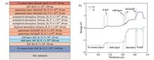
ObjectiveMicrowave photonics (MWP) seamlessly integrates microwave technology with photonics, harnessing the strengths of both to enable long-distance transmission and efficient processing of microwave signals. By encoding microwave signals onto optical signals and utilizing optical fibers for transmission, MWP offers significant benefits such as large bandwidth, low loss, and strong anti-interference capabilities. This technology finds wide application in various fields, including long-distance communication, radar array systems, and radio frequency (RF) signal processing. Balanced photodiodes (BPDs) are essential components in analog photonics transmission links, effectively mitigating relative intensity noise from laser sources and amplified spontaneous emission noise from erbium-doped fiber amplifiers (EDFAs). Therefore, the development of high-power and high-speed balanced photodiodes is crucial for achieving high link gain, low noise, and a large spurious-free dynamic range in microwave photonics transmission links. Traditional PIN photodetectors suffer from limitations in bandwidth and output power due to the slow drift velocity of holes and serious space-charge effects. Uni-traveling carrier photodetectors (UTC-PDs) have been demonstrated to overcome these limitations by separating the absorption and drift regions. In UTC-PDs, light is absorbed in the heavily doped P-type absorption layer, generating electron-hole pairs. The photo-generated holes are then collected by a metal contact via dielectric relaxation, allowing only electrons with high mobility to drift to the collection layer. In this study, a high-speed and high-power modified uni-traveling carrier balanced photodiode is demonstrated through flip-chip bonding on a diamond submount.MethodsThe epitaxial layer structure of the balanced photodiode is optimized. A 50 nm thick P-type doping charge layer is introduced to regulate the electric field in the drift layer, enabling electron overshoot. Additionally, a stepped doping undepleted absorption layer, with a thickness of 120 nm, is adopted to generate a stepped potential distribution, thereby accelerating the diffusion of electrons. Furthermore, a 40 nm depleted absorption layer is implemented to provide a high electric field, alleviating the accumulation of carriers and mitigating carrier blocking at the interface between the absorption layer and the drift layer. InGaAsP quaternary layers are utilized to smooth the band discontinuity and mitigate carrier blocking. Simultaneously, a cliff layer is incorporated to enhance the electric field across the heterojunction interface. In the fabrication process, the active region is defined by double mesa structures, which are dry-etched. Metal stacks are employed to form good ohmic contacts with InGaAs and InP contact layers, respectively. Subsequently, a 255 nm thick SiO2 layer is deposited on the back of the polished InP substrate as an anti-reflective (AR) coating. Finally, the wafer is diced into 1.0 mm×1.3 mm chips. To enhance heat dissipation, the diced chips are flip-chip bonded onto diamond submounts with high thermal conductivity employing the FineTech FINEPLACER? pico system.Results and DiscussionsLumerical 3D model simulations are conducted to analyze the energy band diagram and frequency response of the high-speed and high-power modified uni-traveling carrier balanced photodiode, validating the feasibility of the optimization scheme. Subsequently, to verify the performance of the balanced photodiode, we test and analyze the characteristics of the device-including dark current, responsiveness, frequency response, and saturated output power. The fabricated back-illuminated balanced photodiodes exhibit approximately 200 nA dark current [Fig. 3(a)] and a responsivity of 0.12 A/W at a -3 V bias voltage. Utilizing a vector network analyzer with a scanning frequency range from DC to 67 GHz, the S11 parameters of the device are measured. Combined with the equivalent circuit model of the balanced photodetector, this facilitates the extraction of the device’s physical parameters to analyze the resistor capacitance (RC) limited bandwidth and transit time-limited bandwidth. The junction capacitances of one-side devices with diameters of 4, 6, 8, and 10 μm are 3.8, 8.5, 15.2, and 23.7 fF, respectively. Additionally, the parasitic capacitance is approximately 33.0 fF [Fig. 3(c)]. Finally, to measure the frequency response of the balanced photodetector devices, we establish a test system (Fig. 4). The 3 dB bandwidths at differential mode are 52, 42, and 40 GHz, corresponding to diameters of 4, 6, and 8 μm, respectively (Fig. 5). Notably, RF output powers of 14.0 dBm at 47 GHz and 8.0 dBm at 50 GHz are achieved (Fig. 6).ConclusionsA back-illuminated modified uni-traveling carrier balanced photodetector is proposed. The introduction of a 50 nm thick P-type doping charge layer regulates the electric field in the drift layer, enabling electrons to overshoot and effectively improving the bandwidth of the balanced photodetector. Simultaneously, flip-chip bonding technology is developed to achieve heterogeneous integration of the balanced photodetector chip with a high thermal conductivity diamond substrate, effectively reducing the core temperature of the device and increasing the output power. The back-illuminated balanced photodiodes exhibit ~200 nA dark current and 0.12 A/W responsivity at a -3 V bias voltage. The 3 dB bandwidths at differential mode are measured at 52, 42, and 40, with diameters of 4, 6, and 8 μm, respectively. Notably, RF output powers of 14.0 dBm at 47 GHz and 8.0 dBm at 50 GHz are achieved. While the proposed back-illuminated modified uni-traveling carrier balanced photodetector has shown performance improvement around 50 GHz, it is noted that lower coplanar waveguide (CPW) inductance and reduced parasitic capacitance are still needed to further increase output power at high frequencies.
Jul. 10, 2024Vol. 44 Issue 13 1304001 (2024)
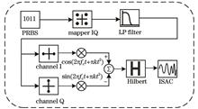
Yanqun Zuo, Feng Zhao, Jin Wang, Qiang Qian, Shuaishuai Hou, Yunfei Duan, and Lingjie Kong
ObjectiveWith the maturity and commercialization of 5G/5G-A technology, research on 6G technology has been on the agenda. As a more advanced next-generation mobile communication technology, 6G technology has stronger service capabilities and has gradually evolved from a simple communication service to a complex service integrating communication, sensing, and computing power. Additionally, in the future, the application scenarios of 6G technology will be more extensive, and be applied to smart healthcare, smart transportation, smart cities, smart factories, and other fields. In these application scenarios, communication services and sensing services should be included at the same time. Therefore, in the future, 6G networks should have both communication and sensing capabilities. In short, in the future 6G communication network, communication and sensing functions will be highly integrated, and gradually evolve into communication and sensing integration. With the continuous development of new services, the demand for high-speed data transmission and low-latency communication is growing day by day, but the current wireless frequency band cannot meet this demand. Thus, it is necessary to explore higher-frequency bands, and meanwhile the terahertz bands with rich spectrum resources are suitable for the application scenarios of ultra-high-speed communication transmission and can meet the needs of current and future communication networks. Therefore, we conduct a generation and transmission analysis on multi-order quadrature amplitude modulation and linear frequency modulation (MQAM-LFM) signals of optical carrier terahertz with integrated sensing and communication (ISAC). Additionally, a single intensity modulator is adopted to generate a terahertz ISAC signal, which can achieve high-speed communication and high-precision perception and provide references for the development of 6G communication and sensing integration technology in the future.MethodsWe employ MATLAB and VPI Transmission simulation softwares. First, a certain number of pseudo-random binary sequences are generated by MATLAB, and the constellation diagram is utilized to map the higher-order vector signal. Then this signal is modulated to the chirp carrier, the digital signal is converted into an analog signal via the digital to analog converter (DAC), and then the Mach-Zehnder modulator (MZM) is driven. Specifically, the MZM works at the orthogonal bias point, and the phase difference of the upper and lower arm drive signals is 90°. After passing through the modulator, a single-sideband (SSB) ISAC optical signal is generated, and then a certain distance is transmitted in the single-mode optical fiber. Meanwhile, the ISAC signal in the terahertz band is generated by beating with another light source.Results and DiscussionsThe proposed ISAC signal can achieve high-speed communication and high-precision perception. The ISAC signal of SSB can be generated by employing a single MZM, which can reduce the influence of fiber nonlinear effects [Fig. 2(b)]. The integrated signal generated by this scheme is more correlated, the perception results can be adopted to assist with communication synchronization, and the fuzzy function plot is closer to the pushpin shape, which leads to better perception performance (Fig. 4). The SSB-integrated signal generated by this scheme has a suppression of about 26 dB of the lower sideband signal (Fig. 5). Experiments show that the proposed scheme can successfully implement the communication function (Figs. 6 and 7). After theoretical derivation, the ISAC signal can detect the maximum distance of 16.88 m (Fig. 8). Research on the sensing performance of the integrated signal shows that the sensing performance of the integrated signal is better than that of the LFM signal with smaller perception error (Figs. 10 and 11). The study of communication and perception performance boundary analysis indicates that the system can achieve a communication rate of up to 40 Gbit/s and a sensing resolution of 1.3 cm (Table 3). In the further study of communication and perception performance, when the roll down factor is 0.313, the overall performance of the system is the best and the spectrum utilization can reach 2.76 b/(s·Hz) (Fig. 12).ConclusionsWe employ a single MZM to successfully generate ISAC signals in the terahertz band, which adopts high-order vector modulation and linear frequency modulation signals, and thus has a high communication rate and sensing accuracy. Theoretical analysis reveals that the ambiguity function of the MQAM-LFM integrated signal is closer to the pushpin shape. Simulation experiments demonstrate that the communication quality of the integrated signal is inferior to that of the traditional QAM signals due to the nonlinear effects during the modulation and transmission process. However, in the target measurement experiments at different distances, the perception performance of the integrated signal is better than that of the LFM signal with a smaller ranging error. In the further study of communication and perception performance, when the roll down factor is 0.313, the overall performance of the system can reach the optimum, and the spectrum utilization rate of the system is 2.76 b/(s·Hz), with a perceptual resolution of 1.62 cm. The above experiments show that the system can achieve a communication rate of up to 40 Gbit/s and a sensing accuracy of 1.3 cm.
Jul. 10, 2024Vol. 44 Issue 13 1306001 (2024)
Li Mei, Shaochun Ma, Zhenzhu Xu, Shoubao Han, and Yuhua Chong
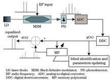
ObjectiveIn recent years, microwave photonic technology has caught extensive attention in electronic information equipment due to its low transmission loss, ultra-wideband, and high amplitude-phase consistency. Since Mach-Zehnder (MZ) modulators have inherent nonlinear characteristics, the electro-optic modulation of radio frequency (RF) signals will induce nonlinear distortions. For applications such as optical beamforming, optical analog-to-digital conversion, and optical frequency conversion which integrate electro-optic modulation into RF analog transceivers, the nonlinear distortion caused by electro-optic modulation will reduce the spurious-free dynamic range (SFDR) of RF transceivers. This in turn limits the application and advancement of microwave photonic technology. Thus, we address the nonlinear distortion in microwave photonic links with blind identification and digital compensation methods. By adopting these methods, the SFDR of microwave photonic links can be improved without modifying the original microwave photonic systems.MethodsBy converting the output of microwave photonic link into digital signals by the high-speed analog-to-digital converter, digital signal processing techniques that employ blind identification compensation can be utilized to suppress the link’s nonlinear distortion (Fig. 2). The digital signal is first converted to an intermediate frequency (IF) signal via digital down-conversion, and then a memory polynomial model is leveraged to fit the nonlinear intermodulation distortions within the signal. This fitted distortion is subtracted from the original IF signal to achieve nonlinear distortion suppression. We propose employing a spectrum reduction algorithm based on time-frequency transformation to blindly identify the high power signal and distortions within the IF signal. The processing enables the parameter extraction for the memory polynomial model. The IF signal is first transformed into the frequency domain using the fast Fourier transform (FFT). By setting a power threshold in the frequency domain, the separation of high-power signals from low-power signals is achieved. Subsequently, by applying the inverse FFT, the separated high-power and low-power signals are converted back to the time domain, thus yielding a high-power signal that approximates an undistorted ideal signal, and a low-power signal containing nonlinear distortions. By adopting the high-power signal as an input, a first memory polynomial model is employed to fit the components of nonlinear distortion in the low-power signal, and the parameters of the nonlinear model are extracted using the least squares method. By fitting the nonlinear distortion with the first memory polynomial model and adding it to the high-power signal as input for a second memory polynomial model, the nonlinear distortion components in the low-power signal are fitted again to yield the final parameters of the nonlinear model. Additionally, we obtain the nonlinear model parameters by this two-stage fitting process, which can enhance the digital nonlinear compensation effectiveness in microwave photonic links with strong nonlinear distortion.Results and DiscussionsWe employ measured data from the microwave photonic link transmission of a two-tone signal centered at 13.8 GHz to perform offline processing, validating the proposed digital nonlinear compensation method (Fig. 4). By adopting single nonlinear fitting for digital compensation, the third-order intermodulation (IMD3) suppression of the compensated signal is 41.7 dB, an improvement of approximately 18 dB compared to the original signal [Fig. 4(a)]. By utilizing the proposed twice nonlinear fitting for digital compensation, the IMD3 suppression of the compensated signal is 60.7 dB, an increase of 37.1 dB compared to the original signal [Fig. 4(b)]. Meanwhile, there is also a significant improvement in the fifth-order intermodulation suppression. We conduct digital compensation processing using the proposed twice nonlinear fitting on 72 sets of two-tone signals with center frequencies ranging from 2.6 to 16.8 GHz (Fig. 5). After digital compensation, the two-tone signals show an IMD3 suppression of approximately 48 to 62 dB, which shows an improvement of 22 to 46 dB over the uncompensated signals.ConclusionsWe introduce a blind separation method for nonlinear distortion compensation of microwave photonic links based on the spectrum power threshold of the optical link output. Furthermore, we propose a digital compensation technique that employs twice nonlinear fitting to suppress intermodulation distortions in microwave photonic link with significant nonlinearity. Additionally, a high-speed oscilloscope is adopted to sample the output signal of a microwave photonic link, and then offline digital compensation is performed. The nonlinearity of the optical link is fitted and digitally compensated using a memory polynomial model with a nonlinear order of 5 and a memory depth of 16. Finally, this approach improves the IMD3 suppression of the microwave photonic link by more than 20 dB across the frequency range from 2.6 to 16.8 GHz.
Jul. 10, 2024Vol. 44 Issue 13 1306002 (2024)
Jinwang Li, Haifeng Yao, Keyan Dong, Yuguang Yang, Yansong Song, Yan An, and Tianci Liu
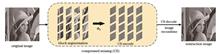
ObjectiveSpace laser communication technology combines the advantages of fast laser communication speed, wide bandwidth range, good confidentiality, and flexible application in wireless communication. It has gradually been widely utilized and has become a major research hotspot. Optical communication video transmission is undoubtedly an important application scenario for space laser communication. Traditional video transmission methods can deal with cumbersome image data, especially in scenarios such as inter-satellite and satellite-to-ground communications, where data acquisition is challenging. This often causes problems in data transmission and storage, adding considerable stress to storage units. Compressive sensing technology, which combines sampling and compression, bypasses the Nyquist sampling theorem, significantly reducing data in the link and alleviating pressure on the transmission channel. Although the current traditional block compressive sensing (BCS) algorithm improves the processing speed of compression reconstruction, it applies a unified sampling rate to each block, despite the different image information contained in different blocks. When the image content is divided into target and background, then the current processing mechanism typically under-samples the target and over-samples the background, leading to low data utilization and suboptimal reconstructed image quality. Therefore, we need to consider the status of different image blocks and further optimize the algorithm.MethodsWe focus on space laser communication video transmission. It uses the image centroid as the judgment feature value, calculates the centroid error between frames, and evaluates the changing speed of the image block. This approach helps determine the sampling rate for the current frame image and generate a measurement matrix by reducing the sampled data for blocks with high inter-frame correlation and increasing the sampling rate for blocks with low inter-frame correlation and overall data utilization. Then, we use FPGA as the main control chip to build an experimental system for video image compressive sensing transmission and reconstruction. The system tests the video image transmission under spatial light, comparing the reconstructed image results between the proposed algorithm and the traditional algorithm.Results and DiscussionsWe simulate this algorithm based on a set of natural scene video extraction image sequences, setting the total sampling rate to 0.1. Each frame of the image is compressed and reconstructed using this algorithm. At the same time, a comparative experiment is conducted with the traditional BCS algorithm at the same sampling rate, comparing the corresponding reconstruction results of different frame images (Fig. 3). At low sampling rates, other algorithms produce reconstruction results with significant random noise and blur, affecting image quality. However, the proposed algorithm achieves good reconstruction and restoration of image details. To further evaluate the algorithm’s performance, we use some typical metrics such as the image peak signal-to-noise ratio (PSNR), structural similarity (SSIM), normalized root mean square error (NMSE), and gradient magnitude similarity deviation (GMSD). Under multiple groups of specified sampling rates, the average values of the multi-frame reconstructed image data indicators are compared (Figs. 4 and 5). The proposed algorithm outperformed others in various performance indicators at different sampling rates. Especially when the sampling rate is extremely low, the traditional typical measurement matrix can hardly reconstruct the original image, while our algorithm can basically retain the characteristics of the original image. Taking the sampling rate of 0.1 as an example, the average PSNR value is about 8 dB higher, and the overall average SSIM is more than 9% higher than that of other algorithms. We develop a spatial optical video transceiver board based on FPGA chips and build two spatial optical video transmission principle terminals. Using a communication rate of 1.25 Gbit/s, we use frame-by-frame transmission to collect 1550 nm wavelength optical video stream signals and sample a total of 200 frames of video image sequences as data for the transmission experiment. In our experiments, the receiver collects compressed image sequences for reconstruction and solution, and further combines all reconstructed images to obtain a video (Fig. 8). At a 0.2 sampling rate, the PSNR of reconstructed video images by our algorithm is generally higher than 35 dB, which is generally more than 5 dB higher than that of other algorithms. At the same time, SSIM indicators have also improved by more than 8% compared with other algorithms.ConclusionsWe propose a method for video compression transmission in space laser communication systems by optimizing the traditional compressive sensing algorithm through the comparison of centroid differences between video image frames. The image block sampling rate and measurement matrix are designed based on the distance between each image block and the center of mass and the degree of image change between frames. This method improves the sampling efficiency of compressive sensing to a certain extent and reduces the impact of block oversampling and undersampling on image reconstruction quality in traditional sampling schemes. At the same time, we built an algorithm principle hardware testing system based on FPGA to provide a guarantee for the experimental verification of the algorithm. Experimental results show that compared with the traditional block compressive sensing algorithm, the proposed algorithm reconstructs video results with better quality, particularly at low sampling rates, providing better reconstruction effects for each frame of image in the video stream, which has certain practical value.
Jul. 10, 2024Vol. 44 Issue 13 1306003 (2024)
Yunfei Duan, Feng Zhao, Yanqun Zuo, Jin Wang, Shuaishuai Hou, Lingjie Kong, and Qiang Qian
ObjectiveWith the increasing frequency of mobile communication systems and wide application of large-scale antennas, mobile communication systems and radar systems have similarities in many aspects, including spectrum utilization, MIMO transmission, and beamforming technology. The integration of perception and communication will be an important direction in the development of 6G technology, and high-rate communication and high-precision perception is a key 6G technology. The terahertz frequency band (0.1-10 THz) is rich in resources, which can support ultra-high rate wireless communication and precision perception. With its inherent characteristics of large bandwidth and parallel processing, it can break through the bottleneck of the electronic bandwidth of the terahertz system. The existing integrated terahertz communication and sensing system can not provide simultaneous measurement of distance and speed, and the range offset can not be eliminated in the single frequency modulation slope linear frequency modulation (LFM) radar, without the ability to provide the simultaneous measurement of distance and speed independently. Thus, further research is needed on the integration system of terahertz communication and perception. Combining photonics technology to design an integrated signal of high-speed communication and high-performance perception is a development direction in the integration of terahertz communication and perception.MethodsTo solve the above problems, we propose a bilinear frequency modulated optical terahertz communication and sensing integrated signal. The carrier frequency is 255 GHz, the communication modulation format is probabilistic shaping 64-order orthogonal amplitude modulation (PS64QAM), and the sensing signal is a dual linear frequency modulation (DLFM) signal, with the integrated signal generated by time division multiplexing (TDM) technology. The generation, transmission, and reception of terahertz signals are carried out by MATLAB and VPI co-simulation. Additionally, digital signal processing is employed to recover and extract information from communication perception signals.Results and DiscussionsPS64QAM-DLFM terahertz communication and sensing integrated signals are generated by TDM technology and photon-assisted technology, and the performance of communication and sensing can be flexibly controlled by adjusting the time-width ratio of communication and sensing signals. In the 255 GHz band, when the wireless transmission distance is 10 m and the time-to-width ratio of the all-sensing signal is 3∶5, a balance is struck between the communication and sensing performance. The communication rate is 31 Gbit/s, the distance resolution is 7.5 mm, and the speed resolution is about 114 m/s, with a ranging accuracy of about 7 mm and speed measurement accuracy of about 15 m/s. As shown in Fig. 12 and Table 2, with the continuously rising distance and speed, ranging and velocity measurement errors become increasingly larger. As shown in Fig. 11, the system can achieve a centimeter-level ranging function under moving targets, which is not available in the existing optical terahertz communication and sensing integrated system.ConclusionsThe proposed integrated signal can complete simultaneous communication distance and speed measurement. Compared with the existing optical terahertz communication and sensing integrated systems, the integrated signal communication terminal can achieve low-error performance thanks to probability shaping technology. In terms of perception, DLFM technology solves the fuzzy problem of the joint distance and speed measurement, and can still accurately detect the target distance in high-speed moving conditions. This proves that the integrated signal has the ability of high-speed communication and high-resolution radar ranging and velocity measurement, with broad application prospects in the future 6G communication.
Jul. 10, 2024Vol. 44 Issue 13 1306004 (2024)
Qian Liu, Pufeng Gao, Shiyi Cai, bin Yin, Beilei Wu, Mingjian Zhu, Desheng Chen, and Muguang Wang
ObjectiveFiber optical magnetic sensors have gained significant interest due to their small size, corrosion resistance, and ability to operate in harsh conditions. Typically, these optical fiber-based sensors are optically demodulated employing an optical spectrum analyzer (OSA) to monitor wavelength shifts or power variations, but this method suffers from slow scanning rate and poor resolution. Therefore, it is essential to suggest a magnetic sensor with a fast interrogation speed and high resolution to meet the needs of certain application fields, such as subsea weak magnetic field detection and exploration of Earth’s mineral resources. Recently, optoelectronic oscillator (OEO)-based magnetic field sensing methods have been proposed with different fiber structures, such as fiber Bragg grating (FBG), Mach-Zehnder interferometer (MZI), and FBG Fabry-Perot (FBG-FP) filter. By mapping the sensing information to the frequency of the microwave signal generated from the OEO, the interrogation speed and resolution of the sensor can be strengthened. However, OEO-based magnetic field measurement using FBG and MZI exhibits low sensitivity, and the utilization of FBG-FP or phase-shifted FBG, characterized by narrow notches in their reflection spectrum, proves to be expensive and challenging in manufacturing. In this paper, we put forward an OEO-based highly sensitive magnetic field sensing scheme utilizing an extrinsic fiber Bragg grating Fabry-Perot (EFBG-FP) filter. The proposed scheme not only mitigates the complexity and cost associated with manufacturing the sensing probe but also significantly enhances the sensitivity of magnetic field sensing.MethodsWe use a pair of FBGs to construct an EFBG-FP filter, with both end faces being carefully milled and axially aligned by the insertion of ceramic ferrules. This is then combined with a grooved magnetostrictive alloy (MA) to create a magnetic field sensing unit. When there is a change in the external magnetic field, the length variation of the MA will effectively induce a change in the air cavity length of the EFBG-FP filter, resulting in a drift in the notch wavelength of the EFBG-FP filter. The EFBG-FP filter exhibits narrowband filtering characteristics. When embedded in the OEO resonant cavity, phase modulation to intensity modulation (PM-IM) can be achieved by filtering one 1st sideband of the phase-modulated signal, and the OEO oscillation frequency will be determined by the difference between the carrier frequency of the light source and the notch center frequency of the EFBG-FP filter. Therefore, the variation in the magnetic field is ultimately mapped to the change in the OEO oscillation frequency. The measurement of the magnetic field can be realized by monitoring the changes in the oscillation frequency with an electrical spectrum analyzer (ESA). In the experiment, the EFBG-FP magnetic field sensing probe is positioned in a solenoid to detect magnetic field changes. To evaluate the sensing performance, the magnetic field is increased in steps of 0.2 mT from 20.2 mT to 21.8 mT, which is within the optimal operating range of the probe, by adjusting the current of the power supply.Results and DiscussionsThe reflection and transmission spectra of the EFBG-FP filter were measured by the OSA with a wavelength resolution of 0.01 nm. The notch’s center wavelength is approximately 1550.022 nm, with a free spectral range (FSR) of about 0.098 nm (Fig. 4). The frequency response is determined using an ESA. The center frequency of the microwave signal generated by the OEO without a magnetic field applied is 1.2116 GHz, achieving a side mode suppression ratio of 57.31 dB (Fig. 5). With the magnetic field increasing from 20.2 mT to 21.8 mT, the OEO oscillation frequency shifts from 1.8540 GHz to 8.6398 GHz (Fig. 6). Fitting results indicate that the magnetic field sensitivity can reach as high as 4.258 GHz/mT, the highest compared to other magnetic field sensing schemes based on OEO (Table 1), with a correlation coefficient (R2) of 99.8% (Fig. 7). The sensing range of our proposed magnetic field sensing system is limited by the FSR of the EFBG-FP filter and the 3 dB bandwidth of the photodetector (bandwidth is 10 GHz) used in the experiment. The theoretical magnetic field resolution of the proposed sensing system is estimated at 0.2 μT. Furthermore, the magnetic field range of 20.2-21.8 mT falls within the optimal operating range for the proposed sensing system.ConclusionsA highly sensitive magnetic field sensing system based on an OEO incorporating an EFBG-FP filter has been proposed and experimentally demonstrated. Two FBGs with reflectivity greater than 95% and well-milled end faces are inserted into ceramic ferrules to form an EFBG-FP cavity, which is bonded to the surface of an MA with two grooves using ultraviolet (UV) glue to constitute a magnetic field sensing probe. With the combination of the OEO, marked enhancements in interrogation speed and resolution are achieved. By simply monitoring the shifts in oscillating frequency, magnetic field measurements can be realized. The proposed sensing system has the advantages of high sensitivity, high resolution, cost-effectiveness, and ease of fabrication. Experimental results reveal that the system can respond to weak changes in the magnetic field. Moreover, by applying a bias magnetic field, highly sensitive magnetic field measurements can be attained over different ranges.
Jul. 10, 2024Vol. 44 Issue 13 1306005 (2024)
Chenxi Su, Yanyu Zhang, Dun Li, Lihui Shen, Qi Wu, and Jian Zhang
ObjectiveIn light of the prevailing limitations of existing indoor positioning methods, including high costs, inadequate positioning accuracy, and susceptibility to external environmental interferences, visible light communication (VLC) using white light LEDs has caught increasing attention as a sustainable and efficient communication method. Owing to the low cost, high efficiency, and extended lifespan of LEDs, indoor VLC positioning technology has emerged as a novel research field. In indoor VLC systems, the layout of light sources is closely related to indoor positioning accuracy. First, it is essential to optimize the layout of the light sources to ensure that the illumination in every corner of the room meets the requirements for both lighting and communication. Second, at the receiving end, it is also crucial to optimize the existing fingerprint positioning algorithms as much as possible and then minimize the average positioning error of the test surface and enhance positioning accuracy. By conducting spatial optimization, positioning LED light sources at appropriate emission locations not only meets the demands for illumination but also improves indoor positioning accuracy. By improving the existing fingerprint positioning algorithms at the receiver end, the average indoor positioning error is reduced. Therefore, in indoor visible light positioning (VLP) systems, the spatial optimization and algorithm improvement are significant for enhancing indoor positioning accuracy.MethodsTo address the aforementioned challenges, we introduce a novel indoor visible light positioning method based on spatial optimization. Initially, the Cramer-Rao bound (CRB) for the test surface is derived, and under the constraints of at least meeting indoor lighting requirements, the optimal layout of LED light sources is simulated by adopting an iterative algorithm. After establishing the optimal light source layout at the transmitter end, the K value associated with the minimum average positioning error is determined by comparing the average positioning errors of the weighted K-nearest neighbor (WKNN) algorithm and the K-nearest neighbor (KNN) algorithm across various numbers of nearest neighbors. To make the distance metric represented by received signal strength (RSS) closer to the actual distance, we should consider the relationship between the actual measurement target and the distance from the LED transmitter. Therefore, based on the received signal strength of the actual measurement target, different weights are assigned to make the RSS-based distance metric more consistent with the actual situation. Compared to the KNN algorithm and the original WKNN algorithm, the improved algorithm significantly enhances the positioning accuracy of indoor visible light positioning systems.Results and DiscussionsThe initial step involves deriving the CRB for the surface to be tested, leading to the identification of the most efficient LED light source layout for optimal localization performance (Fig. 5). The accuracy of this theoretical approach is validated via an iterative algorithm, which compares the light source position coordinates at (1.3 m, 1.3 m) against (1.0 m, 1.0 m). This comparison supported by simulation confirms the correctness of our theoretical derivation (Fig. 6). Table 2 lists the specific parameters of the indoor VLC system. Meanwhile, we compare the average positioning errors of two algorithms at different KNN counts, determining that the WKNN algorithm exhibits the smallest average positioning error under the nearest neighbor number of three (Fig. 8). Subsequently, we compare the average positioning errors and the cumulative probability distributions of positioning errors of three algorithms under different signal-to-noise ratios. Simulation results indicate that the improved algorithm yields an average positioning error of 0.174 m (Fig. 9), representing an increase in average positioning accuracy of 51.12% and 23.34% compared to the KNN and WKNN algorithms respectively.ConclusionsWe initially explore the transmission characteristics of visible light signals in indoor environments and analyze the unique advantages demonstrated by indoor positioning technologies based on visible light communication compared to traditional techniques. The results indicate that the layout of LED light sources significantly influences indoor positioning accuracy. Under the premise of meeting indoor lighting requirements, we derive the CRB for the test surface in a simulated indoor visible light environment, thereby optimizing the layout of the LED light source transmitters. Additionally, the Gauss-Newton algorithm is employed for the iterative estimation of the proposed model. The precision of the theoretical derivations is confirmed by simulation involving two distinct arrangements of light sources and test points to demonstrate the model’s robustness and applicability in varied lighting scenarios. Additionally, we build upon existing location fingerprint algorithms by comparing the performance of the WKNN algorithm with the traditional KNN algorithm. The simulation results indicate that the WKNN algorithm significantly outperforms the KNN algorithm in terms of positioning accuracy when K is 3, thereby demonstrating the effectiveness of the WKNN approach in enhancing location determination accuracy. By making certain improvements and optimizations to the WKNN algorithm, different weights are assigned to different received signal strength differences based on the attenuation characteristics of visible light signals. Simulation results show that the improved algorithm reduces the average positioning error to 0.174 m, enhancing positioning accuracy by 51.12% and 23.34% compared to the original KNN and WKNN algorithms respectively. This significant improvement substantially increases the positioning accuracy of indoor visible light positioning systems.
Jul. 10, 2024Vol. 44 Issue 13 1306006 (2024)
Lin Chen, Hongrong Zheng, Biqiang Jiang, and Jianlin Zhao
Objective45° tilted fiber gratings (45° TFGs) are an important class of polarization-dependent-loss-based polarizers. Unlike other fiber polarizers that require physical modifications to the fiber such as tapering, polishing, and etching the fiber, 45° TFGs can be fabricated noncontactly inside the fiber core with ultraviolet (UV) light exposure, preserving the mechanical strength of the fiber itself. This makes the 45° TFG-based polarizers ideal for applications that prioritize reliability and repeatability, such as polarization-mode-locking fiber lasers and polarization mode filtering in fiber-optic sensing. 45° TFGs utilize the Brewster angle effect, where the s-component of the light propagating in the gratings is resonantly radiated out, and in contrast, the p-component can propagate losslessly in theory. Thus, the contrast between these two polarization components, i.e., polarization extinction ratio (PER), is a fundamental parameter for evaluating the performance of the 45° TFGs. Unlike traditional fiber Bragg gratings, in which their key parameter, reflectivity, grows exponentially with the grating’s index modulation, the PER of 45° TFGs only grows with the square of their index modulation. Hence, a strong index modulation is often required to have a satisfactory PER for many applications. We propose a highly repeatable method to enhance the index modulation of the 45° TFGs and their PER by multi-pass UV light scan.MethodConventional methods for fabricating fiber Bragg gratings (FBGs) include the two-beam interference method, point-by-point writing method, and scanning phase mask method. Specifically, the scanning phase mask is an important technique for fabricating low insertion loss 45° TFGs. It utilizes a tilted phase mask to spatially modulate UV light, creating the desired grating pattern. The UV light is then scanned along the length of the fiber to fabricate a 45° TFG. Due to the limitations of the grating writing system’s stability, traditional writing methods only employ single-pass scanning and do not control the polarization state of the incident UV light. As a result, the full utilization of fiber photosensitivity is not achieved, hindering the fabrication of high index modulation 45° TFGs. To address this, we propose an improved scanning phase mask method, allowing for multiple-pass scan and relaxing the stringent stability requirement of the fabrication system in practice during the entire scanning process required for the high PER 45° TFGs. Our innovative method takes advantage of the UV light polarization control and most importantly real-time feedback of the phase mask position using a high-precision piezoelectric stage integrated into our grating writing system. Using the real-time PER data during the grating fabrication process, a close-loop control is realized for the axial position of the high-precision piezoelectric stage, where the phase mask is mounted. The control parameters are optimized to ensure that the position of the phase mask for the writing segment of the fiber remains unchanged during a multi-pass scan.Results and DiscussionsOur theoretical analysis shows that the polarization control of the UV light enhances its interference fringe contrast after diffracting off the phase mask from about 91% to full 100%, resulting in higher index modulation of our 45° TFG. It is also found that the axial alignment error between successive grating writing passes should be controlled preferably within 10 nm. Experimental results show that with the optimized UV light polarization state and active feedback of the position of the phase mask, 45° TFGs with a center wavelength of 830 nm can be fabricated on hydrogen-loaded 40 μm ultra-thin polarization-maintaining fibers. These gratings only 30 mm in total length, scanned four passes during the writing process, all exhibit a very promising PER exceeding 35 dB, an insertion loss below 2 dB, and a 3 dB wavelength bandwidth exceeding 60 nm. They also demonstrate high annealing stability (only 3% variation) and low standard deviation of PER among multiple samples (0.2 dB), indicating excellent repeatability of our fabrication process and system. These fabricated 45° TFGs are well suited for applications such as fiber-optic gyroscopes and other fiber sensing systems. By reducing the system’s dependence on environmental stability, this adaptive multi-pass grating writing method enables efficient and large-scale production of stable 45° TFGs.ConclusionsWe first theoretically analyze the influence of the polarization state of incident UV light and the position error of the phase mask position during a multi-pass scan on the PER of 45° TFGs. Furthermore, we develop an improved scanning phase-mask fiber grating writing system, incorporating polarization control functionality for the UV light and a high-precision piezoelectric stage to accurately control the position of the phase mask. Real-time PER data obtained during the grating writing process is utilized in our developed closed-loop control algorithm to dynamically adjust the position of the phase mask. This innovative approach enables the development of a multi-pass scan system capable of significantly enhancing the PER of 45° TFGs and most importantly achieving repeatable fabrication of high-performance gratings. The stability and adaptability of the writing system are demonstrated, effectively mitigating environmental influences. Our findings provide a promising solution for the potential mass production of high-performance 45° TFGs, with broad application prospects in fiber-optic gyroscopes and other fiber-optic systems.
Jul. 10, 2024Vol. 44 Issue 13 1306007 (2024)
Sichen Lei, Kouer Yan, Pengfei Wu, Jiao Wang, Zhenkun Tan, and Xiaopeng Yang
ObjectiveOrbital angular momentum (OAM) is an intrinsic property of vortex beams characterized by helical wavefronts. Vortex beams can possess a topological charge of any integer value, with each charge being independent of the others. The superposition and multiplexing of an infinite number of topological charges can significantly enhance the channel capacity and spectral efficiency of communication systems. During the coupling process between optical fibers and waveguides, a technical challenge arises from low coupling efficiency due to mode field mismatch. This necessitates the introduction of a spot size converter (SSC) to improve coupling efficiency. Coupling OAM modes generated within optical fibers with photonic integrated circuits (PICs) holds great significance for providing high-purity mode light sources for on-chip integrated OAM communication. Furthermore, OAM facilitates subsequent signal integrated processing, thus achieving high-capacity system integration.MethodsWe propose a spot size converter that supports multiple OAM modes due to the characteristics of polymer optical waveguide materials, such as low loss, low power consumption, low refractive index, simple fabrication process, low cost, and support for large mode fields. The converter utilizes an SU-8 polymer for the core layer and SiO2 material for the upper and lower cladding layers, featuring a regular polygonal cone structure. The spot size converter is simulated using the Finite Difference Time Domain (FDTD) method in Lumerical software.Results and DiscussionsWe design a spot size converter featuring a regular polygonal cone structure. The optimized dimensional parameters are as follows: H1=5 μm, H2=15 μm, d1=5 μm, d2=2 μm, and L=350 μm, with the polygonal cone having 12 sides (Fig. 2). The mode field output from the optical fiber is coupled into the waveguide of the SU-8 polygonal cone structure which is made of polymer material, along the input direction of the coupler. This process effectively transmits and compresses the mode field carrying orbital angular momentum (Fig. 4). The output optical intensity maintains a donut-shaped distribution, and the phase retains a helical wavefront. This successfully demonstrates the feasibility of using a spot size converter to compress the mode field of the OAM beam in the fiber and achieve coupling with photonic integrated circuits (Fig. 5). The coupling efficiencies of the OAM±1, OAM±2, and OAM±3 modes after the spot size converter are 90.7%, 88.4%, and 86%, respectively. For the source modes OAM±1, OAM±2, and OAM±3, the mode purities are 99.26%, 99.27%, and 98.72%, respectively, with waist sizes of 4.19 μm, 4.61 μm, and 2.87 μm. After beams are passing through the spot size converter, the mode purities are 95%, 99%, and 97%, respectively, with waist sizes of 1.71, 1.91, and 1.38 μm (Fig. 6). A comparison with the method of generating OAM modes within the waveguide shows that our approach achieves higher mode purity, offering a superior quality source for subsequent information processing in PICs. The 1 dB horizontal alignment tolerances for the OAM±1 and OAM±2 modes with the coupler are approximately 2.4 μm and 1.8 μm, respectively. For the OAM±3 mode, the tolerance is about 800 nm, with a 3 dB horizontal alignment tolerance of 2.7 μm. As for the 1 dB vertical alignment tolerances, they are around 2.5 μm and 1.8 μm for the OAM±1 and OAM±2 modes, respectively. For the OAM±3 mode, the tolerance is about 600 nm, with a 3 dB vertical alignment tolerance of 2.6 μm (Fig. 7). The converter’s generous alignment tolerance can simplify the alignment process during the device packaging with the optical fiber.ConclusionsWe explore a spot size converter designed to facilitate the horizontal coupling of high-order OAM modes generated in optical fibers with planar waveguides. Utilizing high-order OAM modes produced by the superposition of LP even and LP odd modes through ±π/2 within the fiber as the source, the coupling of OAM±l, (where l=1-3) modes and optical waveguides is simulated at 1550 nm. The results demonstrate that the spot size converters can achieve stable transmission and compression of the OAM±1, OAM±2, and OAM±3 modes with coupling efficiencies of 90.7%, 88.4%, and 86% respectively. The output mode purities are 95%, 99%, and 97%, respectively. Additionally, the converter exhibits a large lateral and longitudinal alignment tolerance, reducing the technical difficulty of converter and fiber packaging, and facilitating better interconnection with photonic integrated circuits.
Jul. 10, 2024Vol. 44 Issue 13 1306008 (2024)
Yong Chen, Jinliang Zhang, Huanlin Liu, Kaixin Shao, Shangming Chen, Hangying Xiong, and Yourui Zhang
ObjectiveImages can be conceptualized as a vivid linguistic schema that communicates information and elicits emotions via distinct elements comprising lines, colors, shapes, textures, etc. The human visual apparatus demonstrates an elevated sensitivity and recognition proficiency towards these visual components, thereby amassing a lot of information and enriching experience from simple image observations. Additionally, images exert a perceptible influence on human vision. For instance, variations in color, contrast, brightness, and other factors can trigger diversified reactions within the human visual system. However, due to suboptimal environmental lighting, equipment limitations, and the photographer proficiency, the resultant images frequently fail to meet the anticipated outcomes. Among the multitude of factors impinging on image quality, the pervasive influence of environmental lighting conditions, particularly in low-light environments, is the most remarkable. Low-light images can be characterized as images captured in lighting conditions that are insufficient to fully stimulate the brightness capture function of the camera. Consequently, the output image is not even on the fringe of possessing an exemplary histogram distribution. In such predicaments, the implementation of a specialized algorithm becomes imperative to facilitate image enhancement, thereby delivering an optimized image and bolstering overall performance.MethodsTo solve the problems of residual noise, identity mapping in network training, and pairwise data acquisition, we propose a self-supervised low-light enhancement network based on a blind spot network. Firstly, the technique of bilateral multi-scale fusion histogram equalization is utilized to adjust the image brightness and thus overcome the information color loss prevalent in traditional histogram enhancement methods. Secondly, the designed denoising network can adaptively learn from the original image, while pixel shuffle downsampling is employed to decouple the correlation in adjacent pixel spaces. Lastly, related loss functions are designed to maintain the consistency of image space and color.Results and DiscussionsInitially, we delve into the performance of network models with varying stride factors and convolution kernel sizes (Table 1 and Fig. 7). As the stride factor ascends, a parallel increment in model performance ensues, culminating in a peak at stride factor of 5. On the contrary, a continued escalation in stride factor degrades the network performance. As the stride factor widens, the spatial correlation of noise signals decreases, and pixel correlation also diminishes due to an extended distance between the pixels. Only when the noise eradicates a greater proportion of image details, manifesting as aliasing artifacts, does the performance indicator plummet. In contrast, smaller convolution kernels have proven their supremacy in effective image detail capture. To measure the effectiveness of our proposed method, we conduct a comparative experimental analysis using 11 diverse methodologies. Meanwhile, we employ four tangible evaluation metrics, including peak signal-to-noise ratio (PSNR), structural similarity (SSIM), color deviation (Delta E), and natural image quality evaluation (NIQE). During utilizing the LOL test set, outcomes indicate certain limitations inherent to traditional methodologies (Table 2 and Fig. 8). These limitations range from handling local optimal solutions and resulting ramifications of lackluster color, deficient brightness, and conspicuous noise, to consequential discrepancies in color and brightness, blurring, and obscured details. However, our proposed method exhibits remarkable superiority and succeeds in visually retaining the input image color and aligning the overall image brightness much closer to the real image. Furthermore, against the backdrop of most existing enhancement techniques, our proposal stands out with preeminent outcomes across defining evaluation metrics. Additionally, we perform multiple generalization evaluation experiments inclusive of enhancing low-light images captured in actual world settings (Fig. 9). The performance of our proposed method is sound, and features optimum brightness, homogeneous color dissemination, and vividly delineated details. Eventually, we quantify the influence of the loss function on image enhancement by ablation experiments (Table 3 and Fig. 10). Meanwhile, we discover that the custom-designed loss function has a profound bearing on the images, thereby authenticating its efficacy. In summary, when juxtaposed with other available strategies, the proposed algorithm demonstrates superior efficacy.ConclusionsWe propose an enhancement method for low-light images based on blind spot network. The low-light image enhancement task is divided into two sub-tasks of enhancement and denoising, and a set of loss functions without reference is designed to guide network training. By adopting a self-supervised enhancement technique, the limitation of paired data required by many traditional enhancement algorithms is overcome. Meanwhile, blind spot convolution technology is employed to ensure that the identity mapping phenomenon is avoided during the training, which can enhance the network robustness, remove the noise generated during the enhancement, and improve the generalization ability. The experimental results show that our method is superior to the existing methods in image quality and visual effect. At the same time, it is also compared with some other classical image enhancement algorithms, which proves that this method has certain advantages and can provide references for the enhancement of low-light images.
Jul. 10, 2024Vol. 44 Issue 13 1310001 (2024)
Shengjie Liu, Junwei Li, Hao Chen, and Shengqian Wang
ObjectiveTo meet the imaging requirements of high resolution and large field-of-view, infrared target detection optical systems should utilize complex optical lens groups, which results in large volume, weight, and total system length. As a result, they are not suitable for deployment on optical payload platforms with limited space, such as airborne and spaceborne platforms. The infrared fiber image bundle is soft and easy to bend, and adding this kind of bundle to the traditional optical system can flexibly change the optical path and shorten the overall length of the system. However, infrared fiber image bundle optical systems have the nature of spatially double discrete sampling effect, and their imaging characteristics are different from those of traditional optical systems. This makes the traditional target detection signal-to-noise ratio (SNR) formula applicable to linear space-invariant systems and no longer applicable to infrared fiber image bundle optical systems. To this end, we present an innovative method for quantitatively analyzing the target detection capability of infrared fiber image bundle optical systems. The proposed method adopts statistical analysis to complete the derivation of the target SNR and the SNR attenuation coefficient formulas, featuring clarity, simplicity, and easy calculation. We hope that this method will contribute to the optical design, device selection, and system detection capability analysis of infrared fiber image bundle optical systems.MethodsThe target detection scenario of infrared fiber bundle optical systems is set to detect distant point targets under a uniform background in the sky. Thus, the signal and noise components are appropriately corrected respectively to obtain the target detection SNR formula of these systems. First, the overall transmittance of infrared fiber bundle optical systems is obtained by combining the product of the fiber transmittance and the fiber bundle filling factor, the transmittance of the front telescopic system, and the transmittance of the rear coupling system. Then, the proportion of the cross area between the core area of the fiber bundle and the photosensitive area of the detector pixel is defined as the system filling factor, which is employed to characterize the spatially double discrete sampling effect. By utilizing the overall transmittance and filling factor of optical systems, the noise equivalent temperature difference can be statistically derived, and then the noise equivalent power can be obtained, which represents the noise component of infrared fiber bundle optical systems. For the signal component correction, the introduction of the pulse visibility factor is to describe the energy concentration of infrared fiber bundle optical systems on the point target image. Based on the correction formulas for the above-mentioned noise and signal components, a target SNR formula for infrared fiber bundle optical systems is derived, which includes target radiation characteristics, background radiation characteristics, optical system parameters, and detector parameters. To simplify the analysis of system detection capability, we define the SNR attenuation coefficient as the proportion of SNR decrease in infrared fiber bundle optical systems compared to traditional optical systems. Finally, combined with the derived SNR attenuation coefficient and designed structural parameters of the infrared fiber bundle optical system, the system filling factor and pulse visibility factor are calculated, and the relationship between the fiber transmittance and the SNR attenuation coefficient is given. Finally, this can quantitatively evaluate the difference in the detection ability of the infrared fiber bundle optical system.Results and DiscussionsIn the condition of vertical coupling alignment assembly (or matching a certain column of vertical fiber bundle images with a square pixel line array), we combine the optical design results of the point spread function (PSF) of the front telescopic system and the rear coupling system (Fig. 8), and the fiber bundle characteristic function distribution (Fig. 9). Meanwhile, the average pulse visibility factor of the infrared fiber bundle optical system with the fiber bundle resolution of 25×256 toward the point target is calculated to be 0.1335. Due to the coupling mismatch between the infrared fiber bundle and the square pixel array, the fiber coupling area varies for different pixels (Fig. 13), with the calculated average filling factor of 0.4201. Based on the calculated pulse visibility factor and system filling factor of the infrared fiber bundle optical system and the traditional optical system, the relationship between the detection SNR attenuation coefficient ASNR and the fiber transmittance τfiber is given (Fig. 14), and the following conclusions can be drawn. Under τfiber>0.9, ASNR<0.5; under τfiber<0.3, ASNR>0.7; under τfiber<0.03, ASNR>0.9. Therefore, it is advisable to adopt fiber bundle devices with high transmittance to improve the detection capability of fiber bundle systems.ConclusionsWe propose an innovative quantitative analysis method for the ability of infrared fiber bundle optical systems to detect distant targets, thereby solving the problem that traditional target SNR formulas are not applicable to such optical systems with spatially double discrete sampling effect. Based on the imaging theory of infrared fiber bundle optical systems, the target SNR formula is derived by appropriately modifying the signal expression and noise expression. Additionally, the SNR attenuation coefficient expression of the system compared to traditional optical systems is provided, which can effectively characterize the detection ability of the system. Based on the designed infrared fiber bundle optical system, key performance parameters such as the pulse visibility factor and system filling factor are simulated and calculated. The relationship between the fiber transmittance and SNR attenuation coefficient is further analyzed, with the detection ability differences between the two types of optical systems quantitatively compared. The simulation results demonstrate the influence of the spatially double discrete sampling effect on the infrared fiber bundle optical system and clarify that the SNR attenuation coefficient is related to a fixed coefficient of 0.5459 and fiber transmittance. Thus, it is indicated that the detection capability of the system can be improved by selecting fiber bundle devices with high transmittance. Finally, we can provide a theoretical basis for determining the detection ability boundary of infrared fiber bundle optical systems.
Jul. 10, 2024Vol. 44 Issue 13 1311001 (2024)
Songlin Liang, Huirong Zhang, Yanghai Wu, Hui Luo, Bin Li, Chunyan Guo, Yongqiang Yang, Zubang Zhang, and Zhicheng Sun
ObjectiveWhen the optical materials generate heat or the ambient temperature changes, they often affect the normal working state of the optical systems. Thus, it is significant to master the thermal performance parameters of the materials for designing optical systems. Among the parameters, thermal expansion coefficient α and temperature coefficient of refractive index dn/dT are the two most commonly employed basic physical parameters. By measuring two of the three parameters including α, γ (temperature coefficient of optical path), and W (thermo-optic coefficient) using interference method, α and dn/dT can be deduced. There are various forms of optical route implementation, among which the “thermal-optic coefficient measurement instrument” based on the Mach-Zehnder (MZ) interferometer features a simple structure and free sample expansion, without additional clamping stress. Thus, we establish a set of instruments using this scheme, analyze the main error sources, and try to suppress or eliminate them. Finally, we conduct verification on quartz glass samples.MethodsIn the “thermal-optic coefficient measurement instrument”, the thermo-optic coefficients W can be measured from MZ interference results, and the temperature coefficient of optical path γ can be measured from the Fabry-Perot (FP) interference occurring between the sample end faces. Then α and dn/dT can be calculated from them. The optical path difference of FP interference is the optical path between the front and back surfaces of the sample, which is only related to the interior of the sample and is unaffected by other external factors, leading to high stability. However, the MZ interference optical path is influenced by many factors, including the FP interference effect in the sample, mechanical deformation outside the sample, and temperature drift. Therefore, the main error sources in this testing system are waveform distortion and zero drift phenomena in the MZ interference. Meanwhile, theoretical analysis shows that waveform distortion is caused by the influence of FP interference mixed in MZ interference. The results include two aspects of signal amplitude modulation and the addition of additional phases to the signal phase, which are characterized by small, periodic, and zero mean values. The method of directly measuring phase, such as phase modulation, can be employed to avoid the influence of waveform distortion and obtain the measured Δ[(n-1)L]. The monitoring results of the zero drift effect indicate that there is a significant zero drift during the constant and variable temperature processes of the interferometer. Under the sample length of 10 mm, temperature measurement range of 20-120 ℃, and heating rate of 0.5 ℃ per minute, systematic errors of 2.3×10⁻⁸/℃ and 5.7×10⁻⁷/℃ are yielded respectively. By improving the optical path, the beam is expanded to partially pass through the sample and partially not. The part that does not pass through the sample is called the background interference, whose measured optical path difference represents the zero drift value. The part that passes through the sample is called the sample interference. The measured optical path difference is subtracted from the zero drift to obtain the final measured optical path difference, with subsequent calculations conducted to obtain the thermo-optic coefficient W.Results and DiscussionsMeasurement and verification are performed on quartz glass with low expansion characteristics. The selected sample material Corning 7980 is tested in the temperature range from room temperature to 120 ℃, with a heating rate of 0.5 ℃/min. Comparison among the obtained α and dn/dT and the manufacturer’s data and reference values shows that the results are completely consistent. The maximum deviation between the thermal expansion coefficient and the reference value shall not exceed 5.6×10⁻⁸/℃, and the maximum deviation between the refractive index temperature coefficient and the reference value shall not exceed 7×10⁻⁷/℃.ConclusionsThe “thermal-optic coefficient measurement instrument” based on the MZ interferometer can achieve synchronous measurement of the thermal expansion coefficient and temperature coefficient of the refractive index of optical materials, but there are problems of waveform distortion and zero drift effects. The method of directly measuring optical path difference using phase modulation can eliminate the influence of waveform distortion caused by the FP interference effect. The method of synchronously measuring background interference and sample interference optical path difference can deduct the influence of zero drift effects, and ultimately control the system error caused by zero drift within 3×10⁻⁹/℃. Quartz glass testing indicates that the thermal expansion coefficient and temperature coefficient of refractive index at 632.8 nm are completely consistent with the reference data, which verifies the effectiveness of the error source analysis and suppression methods for the system.
Jul. 10, 2024Vol. 44 Issue 13 1312001 (2024)
Haoxing He, Niannian Chen, Ling Wu, Yong Fan, Xuejiao Zhang, and Chuan Qiu
ObjectiveThe digital photoelasticity method combines optics and digital image processing technology. Digital image processing and numerical calculation can help achieve accurate analysis of optical interference patterns, thereby obtaining accurate stress distribution information. It is of significance for stress analysis problems in scientific research, engineering design, and material testing fields. However, the current digital photoelasticity method adopts a divide and conquer approach, dividing the entire stage into several substeps such as phase shifting, phase unwrapping, and stress separation. Each substep requires high experimental environments such as noise, and the calculation accuracy of each stage is limited by the calculation results of the previous stage. Thus, immediate errors generated in each stage will be introduced into the final stress component. With the development of artificial intelligence, deep learning has gradually been applied to digital photoelasticity methods. However, current deep learning models only involve some research on calculating stress differences, and traditional stress separation methods are still needed to calculate normal stress and shear stress. Therefore, we propose a multi-branch deep learning model based on an encoder-decoder and a simulation dataset construction method for stress analysis tasks. This model improves the efficiency and robustness of stress component calculation while ensuring accuracy.MethodsThe proposed method mainly utilizes the feature extraction ability of convolutional neural networks. Based on the improvement of UNet, residual blocks are employed to replace the convolutional modules of the encoder and decoder, accelerating the convergence speed and improving the feature expression ability of the model. Multiple output layers are added in the output part to adapt to the stress component calculation task. Meanwhile, a simulation dataset is generated using the theory formula of radial compression discs, and the dataset is expanded by operations such as rotation, translation, and cropping to provide data-driven support for SANet. Finally, L2 loss is adopted as the loss function for each branch of the neural network, and the weighted sum of the loss functions for the three branches is leveraged to calculate the total loss.Results and DiscussionsThe experimental results on the simulation test set indicate that SANet can calculate the normal stress and shear stress (Fig. 5). In the noise experiment, our model achieves the highest MSE, PSNR, and SSIM (Table 3). The model is tested using a noise test set with a mean of 0 and an increasing standard deviation (Fig. 7), which indicates that our model has strong noise tolerance. Finally, tests are conducted on real data (Fig. 8). Compared with traditional phased processing methods, this method can avoid the phase unwrapping and stress separation stages that are prone to errors, and achieve stress component calculation in one step.ConclusionsWe propose a deep learning method for calculating stress components. This method introduces residual connections based on UNet and changes the output part to a multi-branch output structure to adapt to the stress component calculation task. To train the model, we construct a simulation training set using the radial compression disc formula and data augmentation methods. Additionally, the comparison is conducted between the two phased methods and the proposed method on simulation test sets, noise test sets, and real test data. The results show that compared to traditional phased processing methods, SANet has the highest accuracy and better robustness in calculating stress components.
Jul. 10, 2024Vol. 44 Issue 13 1312002 (2024)
Zhiyi Xu, Xiaoxin Fan, Jiale Zhang, Shenghang Zhou, Zhenyan Guo, Dan Zhu, Zhishan Gao, and Qun Yuan
ObjectiveWhite light microscopic interferometry is a traditional method for non-destructively measuring the three-dimensional (3D) topography of step microstructures. However, its tendency for low-pass filtering smoothens the 3D topography along sharp step edges, making precise edge detection challenging and affecting the calculation and extraction of linewidth parameters. Moreover, when the depth of the microstructure is smaller than the coherence length of the light source, the batwing effect may generate sharp pulses in the recovered 3D topography at these step edges. Despite these pulses being spurious signals, their high-frequency traits are beneficial for identifying step edges. The microstructure linewidth is determined by the distance between the peak positions of the batwing pulse heights corresponding to the two step edges. The spatial sampling frequency of the 3D topography is constrained by the size of the Airy spot and the detector pixel. Typically, only a few pixels in the linewidth measurement direction are influenced by the batwing effect. It is crucial to note that the accuracy of linewidth measurement is confined to the pixel level, and is determined by the peak location of the batwing pulse heights. In this study, we propose a super-resolution measurement method for microstructure linewidth. It is based on precisely locating the peak positions of batwing heights in white light interferometry, surpassing the system’s lateral resolution. We anticipate that our findings will enhance 3D topography measurement of step microstructures and advance our understanding of the batwing effect.MethodsWe introduce a numerical simulation model for white light interferometry signals, with a specific focus on the batwing effect and its discrete sampling characteristics. The model unveils the slow-varying attributes of the spatial domain orthogonal to the linewidth measurement direction, offering theoretical backing for improving the sampling frequency of batwing pulses in that direction. By harnessing the spurious high-frequency information provided by batwing pulses, we can attain super-resolution measurements for microstructure linewidth. This breakthrough surpasses the optical resolution limitations of the system. First, we apply the center of gravity method to process the interference signals captured by white light interferometry from the step sample. Next, for each step edge, we utilize wavelet transform to identify the peak key pixels in the direction parallel to the edge, which signifies the edge position. Subsequently, precise step edge positions are determined through linear fitting of multiple key pixels corresponding to each edge. Furthermore, we extract linewidth parameters based on the positions of the left and right step edges. In essence, we leverage the high-frequency information of batwing pulses in the orthogonal direction of the linewidth, presenting an effective approach for achieving super-resolution in linewidth measurement.Results and DiscussionsWe conduct measurements on an RSN standard plate (provided by Physikalisch-Technische Bundesanstalt) featuring a standard grating step structure using a self-developed white light interferometry system. The test samples have linewidths of 6, 4, 3, and 2 μm. The step height falls within the coherence length of the light source, while the Airy spot radius of the measurement system is 0.590 μm. Our method yields linewidth measurement results with deviations from the calibration value of 0.011, 0.016, 0.021, and 0.015 μm, respectively (Table 1). These experimental findings demonstrate that our proposed method enables super-resolution linewidth measurement, surpassing the system’s lateral resolution. Furthermore, we explore the effect of sample orientation on measurement accuracy and provided recommended values for both the pitch angle of the sample and the tilt angle within the field of view based on measurement uncertainty. As for the pitch angle, optimal measurement conditions are achieved when interference fringes are aligned nearly perpendicular to the step edge during experimentation. Simultaneously, to ensure precision in linear fitting and peak point positioning, the sample tilt angle should be constrained within a specified range [Eq. (6)]. By meeting these criteria, linewidth measurement accuracy can attain a resolution within a few tenths of the pixel scale of the object surface.ConclusionsWe make full use of the spurious high-frequency information provided by batwing pulses at step edges, proposing a super-resolution measurement method for microstructure linewidth using white light microscopic interferometry. This method surpasses the optical resolution limit of conventional systems. We develop a numerical simulation model to elucidate the relationship between batwing heights and step edge positions. Unlike traditional approaches, we focus on microstructure topography in the vertical step-edge direction. Additionally, we transform abrupt step topography into a gradual change process across multiple pixels, enabling precise positioning of batwing heights at step edges. This facilitates the calculation of high-precision linewidth measurements. In our experiments, we measure four grating regions with varying linewidths in the PTB standard plate, confirming the effectiveness of the method. Overall, our approach offers rapid calculation speeds and broad applicability in post-processing white light interferometry signals.
Jul. 10, 2024Vol. 44 Issue 13 1312003 (2024)
Mengxiang Xu, Yi Ni, Yin Xu, Yedeng Fei, and Jun Xia
ObjectiveSilicon-on-insulator (SOI), as a mature on-chip platform, has been widely implemented in photonic integrated circuits (PICs) due to its large relative refractive index difference (2.0) and compatibility with CMOS processes. However, it has noticeable drawbacks. Generating a light source is challenging, and its linear photoelectric effect is absent, making direct modulation of the light field difficult due to the centrosymmetric crystal structure of silicon. In contrast, thin film lithium niobate-on-insulator (TFLN) emerges as an ideal optical platform candidate. It possesses various excellent properties, such as large electro-optic, thermo-optic, and acoustic-optic coefficients, as well as nonlinear properties, and stable chemical and physical characteristics inherent to its material properties. Moreover, it offers a wide transparent window (from 400 nm to 5 μm) and relatively high refractive index contrast (0.7) for light field confinement. The TFLN can be obtained from the lithium-niobate-on-insulator (LNOI) wafer utilizing the smart cut fabrication process, readily available from commercial companies. By combining the unique properties of TFLN with the LNOI wafer, numerous high-speed modulation devices have been proposed, positioning TFLN as a promising alternative to SOI in both classical and quantum domains. However, lithium niobate is an anisotropic crystal, and its intrinsic birefringence leads to strong polarization dependence. In practical systems, the purity of polarization significantly affects device performance. Therefore, polarization management devices play a crucial role in this optical integrated platform. Polarizers act as filters, efficiently removing interference modes while preserving the target mode, typically within a single waveguide. Owing to the increasing demand for reconfigurable and multifunctional polarization devices for photonic integrated circuits, we implement a reconfigurable and multifunctional polarizer based on an LNOI platform assisted by phase-change material.Methods The structure of the proposed device is divided into two partsthe triple-waveguide coupler and the polarization control regions. The triple-waveguide coupler contains an α-Si-assisted waveguide in the center and two LNOI ridge waveguides on the sides. Although the involvement of the α-Si nanostrip complicates the fabrication of the device, it provides a new degree of freedom to manipulate the polarization state, overcoming the drawbacks of low mode birefringence in the LNOl waveguide. With the aid of the α-Si nanostrip, the TM polarization mode can achieve phase matching, while the TE polarization mode exhibits significant phase mismatch, enabling the separation or combination of TE and TM modes. The mode polarizer section consists of the lithium niobate (LN) waveguide and the Ge2Sb2Se4Te1 (GSST) loaded on the top center of the LNOI waveguide sidewards. By controlling the state of the GSST, this structure can control whether TE and TM modes pass through the waveguide or not. Due to the large imaginary part of GSST in the crystalline state, efficient absorption loss for the polarization state can be realized by rationally optimizing structure parameters. The working principle is analyzed as follows: when the GSST layer is triggered into the crystalline state, its high refractive index will exhibit a nonuniform distribution in the vertical direction. Consequently, a significant portion of power distribution from the TE and TM modes, whose electric field is polarized in the vertical direction, will be directed into the GSST layer rather than the LN waveguide. Meanwhile, this concentrated power will be effectively attenuated by the GSST block within a certain length due to its high material imaginary part. On the other hand, when the GSST is in the amorphous state with a lower refractive index, the main light field of the TE and TM modes will be distributed in the LN waveguide. Due to the low extinction coefficient of GSST, only a small fraction of the light power conveyed in the LN waveguide will practically not be lost and will continue to flow into the triple-waveguide coupler.Results and DiscussionsBy rationally designing the geometric parameters of the α-Si, the TM polarization mode can achieve phase matching, while the TE polarization mode exhibits significant phase mismatch, enabling the separation or combination of TE and TM modes (Fig. 3). We optimize the geometric parameters of the GSST layer so that the TE and TM modes can be filtered out when GSST is crystalline while minimizing their influence when GSST is amorphous. Consequently, the polarizer exhibits a higher extinction ratio and lower insertion loss at a wavelength of 1550 nm (Fig. 4). By controlling the state of the two pieces of GSST, the proposed device offers four output modes (TE mode, TM mode, TE+TM mode, and None). We simulate the propagation of the electric field at a wavelength of 1550 nm using the 3D finite difference time domain (3D-FDTD) method to study the performance and optimize the structure of the polarizer. With a wavelength of 1550 nm, the extinction ratio of the TM mode is 34.3 dB, and the insertion loss is 0.42 dB. Similarly, the extinction ratio of the TE mode is 34.2 dB, with an insertion loss of 0.27 dB. The device’s performance parameters are analyzed across the wavelength range of 1530 to 1580 nm, covering the communication C band (Fig. 6). As the TE mode is wavelength-insensitive, the extinction ratio remains stable above 33 dB, with an insertion loss of less than 0.3 dB. The extinction ratio of the TM mode is consistently above 32 dB, with an insertion loss of less than 0.5 dB. Additionally, we analyze the manufacturing error tolerance of the device (Fig. 7). The results indicate that the multifunctional polarizer has a high tolerance for manufacturing errors.ConclusionsWe propose a reconfigurable and multifunctional polarizer based on the LNOI platform, assisted by phase-change material. The status of the TE and TM modes can be controlled to achieve four output modes by manipulating the phase state of the phase-change materials. The 3D-FDTD method is employed to study the performance and optimize the structure of the polarizer. The results demonstrate that the device offers four output modes (TE mode, TM mode, TE+TM mode, and None). The length of this polarizer is 69 μm, and the polarization extinction ratio of the TE mode is 34.2 dB, with an insertion loss of 0.27 dB. For the TM mode, the polarization extinction ratio is 34.3 dB, with an insertion loss of 0.42 dB at a wavelength of 1550 nm. In the wavelength range of 1530 to 1580 nm, the polarization splitting ratio is higher than 28 dB. Furthermore, we analyze the manufacturing error tolerance of the device. The results indicate that the multifunctional polarizer has a high tolerance for manufacturing errors. This high-performance polarizer with reconfigurability and multifunctionality has wide potential in integrated optical systems on LNOI platforms. Compared with traditional polarizers, the proposed polarizer offers the advantages of multifunctionality, high performance, and reconfigurability, with broad application potential in reconfigurable intelligent optical interconnection systems on LNOI platforms.
Jul. 10, 2024Vol. 44 Issue 13 1313001 (2024)
Lianlian Du, Jingfang Liu, Jiamin Liu, Rongguo Yang, Hengxin Sun, and Jiangrui Gao
ObjectiveLaser frequency stabilization is an essential technology in various applications, including optic communication, quantum metrology, and space-borne gravitational wave detection. Conventionally, the laser for use is frequency stabilized to an ultra-stable reference cavity. However, the frequency noise due to the cavity length noise of the reference cavity still limits the application of the ultra-high-precision measurement of space-time strain with a magnitude of the order of 10-18-10-20 in the frequency range of mHz-Hz. Before application in such high-precision measurements, extensive suppression of frequency noise is mandatory. The thermal noise of the reference cavity is typically a predominant source that necessitates reduction. Higher-order laser transverse modes, characterized by a larger transverse intensity distribution, yield a lower spatially averaged thermal noise. The integration of higher-order modes into frequency stabilization with ultra-stable cavities has not been exhaustively explored in the literature.MethodsWe first introduce a generalized noise model for frequency stabilization based on a reference cavity. Then we apply this model to higher-order mode reference cavities to scrutinize the influence of the mode transformation noise on the final frequency noise. By controlling a series of technical noises of the cavity such as vibration, temperature, and electronic noise, the thermal noise and shot noise emerge as the two dominant noise sources. According to the fluctuation dissipation theorem, we calculate and compare the thermal noises of higher-order Hermite-Gaussian (HG) and Laguerre-Gaussian (LG) modes, using parameters of a regular ultra-stable cavity. We also delve into the mode coupling efficiencies of different LGp,0 modes based on the scheme of mode-mismatching for mode transformation. The shot noise, attributable to the limited mode coupling efficiency, is also taken into account. By compromising the thermal noise and shot noise, we propose some optimal mode orders for achieving minimal total noise.Results and DiscussionsAccording to the noise transfer model, the noise introduced by the mode transformation is non-negligible, particularly in the presence of a mode-filtering cavity (Figs.1 and 2). Consequently, we implement a simple mode transforming scheme based on the mode mismatching. The mode coupling efficiencies varying with mismatching parameters for higher-order LG modes are given. The thermal noise for both higher-order HG and LG modes is delineated, demonstrating a decrease in noise with an increasing mode order. Owing to the better spatial symmetry, the LG mode exhibits lower thermal noise for the mirror substrate compared to the HG mode at equivalent mode orders (Fig. 4). The frequency thermal noise across the entire reference cavity is calculated (Table 2). When the ULE substrate is changed into fused silica, the fundamental mode thermal noise is reduced from 0.096 Hz/Hz1/2 to 0.029 Hz/Hz1/2. With a fused silica substrate, the reduction rate of thermal noise of the LG10,0 mode at 1 Hz is 16% compared to the fundamental mode. Considering the shot noise, the lowest total noise for the LGp,0 mode in the range of 0≤p≤25 can reach 0.022 Hz/Hz1/2 at 1 Hz, marking a 23% reduction compared to the total noise of the fundamental mode. More results involving different mode order, input optical power, and analyzing frequency are listed (Table 3).ConclusionsWe present a general noise transfer model for laser frequency and extend its application to higher-order mode-based frequency stabilization. The noise associated with mode transfer warrants careful consideration. The thermal noise decreases with increasing mode order. The thermal noise of LG mode is lower than HG mode under the same condition. The dissipation due to the limited mode transfer elevates the shot noise, a factor that should be contemplated for low-power injection and can be weighed against the reduced thermal noise of higher-order modes. The total noise is influenced by various parameters and can be optimized by considering the mode order.
Jul. 10, 2024Vol. 44 Issue 13 1314001 (2024)
Songtao Bai, Zhengru Guo, Kangwen Yang, Yu Xia, Mingyang He, Anqing Hao, and Min Li
ObjectiveDual-comb spectroscopy (DCS) based on optical frequency comb (OFC) has attracted much attention in recent years because of its high sensitivity, high resolution, and high sampling rate. At present, there are three technical routes to achieve DCS: coherent DCS, adaptive DCS, and single-cavity DCS. The single-cavity DCS system is constructed by two pulse sequences with a small repetition frequency difference from a single laser, and the two mode-locked pulse sequences share part or the whole laser cavity, which suppresses common-mode noise and maintains good coherence, making the system possess simple structure, high coherence, and easy integration. Given the advantages above, it has become one of the research hotspots in recent years.MethodsA linear all-polarization-maintaining dual-wavelength mode-locked erbium-doped fiber laser is used in the experiment. The semiconductor saturable absorber (SESAM) is used to assist mode-locking, and the wavelength division multiplexer (WDM) with polarization-dependent loss is fused with the polarization-maintaining erbium-doped fiber to generate a periodic Lyot filter. By adjusting the pump power and the polarization state in the cavity, the laser can switch between single-wavelength and dual-wavelength mode-locked states.Results and DiscussionsWhen the pump power is increased to 60 mW, the laser begins to output continuous light near the central wavelength of 1560 nm. When the pump power is increased to 106 mW, and the wave plate is rotated to adjust the polarization state in the cavity, the laser begins to exhibit a mode-locked state. At this time, the mean output power of the fiber laser is 1.03 mW. In the single-wavelength mode-locked state, the central wavelength of the two pulse sequences is 1564.2 nm, the bandwidth of 3 dB is 2.8 nm, and there are obvious Kelly sidebands on both sides of the spectrum [Fig. 2(a)]. The repetition frequency is 22.81 MHz, the signal-to-noise ratio (SNR) is 52 dB, and the spectrum diagram in the 550 MHz range indicates that the mode-locked laser is stable at this time [Fig. 2(b)]. The two pulse sequences are spaced 43.8 ns apart, corresponding to the repetition rate [Fig. 2(c)]. The autocorrelation curve under Gaussian fitting is 1.4 ps [Fig. 2(d)]. Due to the presence of the Lyot filtering effect, when the pump power is increased to 176 mW, the single-wavelength mode-locking is switched to asynchronous dual-wavelength mode-locking by changing the polarization state in the cavity. The central wavelengths of the two asynchronous pulse sequences are 1563.0 and 1568.4 nm, and the 3 dB bandwidths are 1.6 and 1.3 nm, respectively [Fig. 3(a)]. The repetition frequencies of the two pulse sequences are 22.813252 and 22.813571 MHz, with a repetition frequency difference of 319 Hz, and the SNR is 60.2 and 57.1 dB, respectively [Fig. 3(b)]. The maximum spectral offset of the two center wavelengths in one hour is less than 0.3 nm, and the root-mean-square (RMS) value of power fluctuation is 0.21% [Figs. 3(c) and 3(d)]. Figures 4(a)-4(e) show the fragment diagrams of each time period of the oscilloscope under the asynchronous dual-wavelength mode-locked state. Asynchronous dual-wavelength mode-locking can be converted to synchronous one when the pump power is increased to 460 mW. The central wavelengths of the two pulse sequences are 1562.1 and 1567.3 nm, and the corresponding 3 dB bandwidths are 0.5 and 0.6 nm respectively [Fig. 5(a)]. The repetition frequency is 22.81353 MHz and the SNR is 56 dB [Fig. 5(b)]. A synchronous dual-wavelength oscilloscope trace diagram is shown in Figs. 5(c) and 5(d). To prove whether it is a synchronous dual-wavelength pulse, commercial filters are used to filter out components of different wavelengths. Oscilloscope trajectories of different wavelength components after filtering are shown in Figs. 6(a)-6(c). The maximum deviation of the central wavelength of both pulse sequences in one hour is less than 0.4 nm, and the RMS value of the power fluctuation is 0.17%, indicating that the mode-locked state is stable [Figs. 7(a) and 7(b)].ConclusionsIn summary, the experiment verifies the all-polarization-maintaining dual-wavelength mode-locked erbium-doped fiber laser based on SESAM. A periodic Lyot filtering effect is formed by combining a WDM with the polarization-maintaining erbium-doped fiber. By controlling the pump power and adjusting the polarization state in the cavity, asynchronous and synchronous dual-wavelength mode-locked states can be obtained. Because of the dispersion in the laser cavity, the mode-locked pulses with different center wavelengths have different repetition frequencies, and a repetition frequency difference of ~319 Hz can be formed between the two asynchronous dual-wavelength mode-locked pulses. The research results provide a new method for the realization of all-polarization-maintaining, repeatable, and stable dual-wavelength mode-locked lasers, which is of great significance in the application of DCS.
Jul. 10, 2024Vol. 44 Issue 13 1314002 (2024)
Jianqiu Cao, Zhaode Li, Maoni Chen, Aimin Liu, Zhihe Huang, Zefeng Wang, and Jinbao Chen
ObjectiveHigh-brightness and high-power fiber lasers operating near 980 nm have important applications because they can not only be applied for pumping the ultrafast solid-state and fiber lasers but also generate the emission around 490 nm by frequency-doubling. However, it is difficult to achieve high-power near-diffraction-limited operation for the fiber laser operating near 980 nm. The main reason is that the large core-to-cladding area ratio (CCAR) of the active fiber is needed to suppress the amplified spontaneous emission (ASE) around 1030 nm. Although some micro-structured fibers have been designed for suppressing the ASE around 1030 nm and maintaining good beam quality, their difficult manufacturing and drawing processes limit the popularization of pertinent studies. Therefore, more studies have been carried out by using double-cladding Yb-doped fibers (DCYFs). However, the beam quality achieved by the DCYF is generally poor. Moreover, the strong in-band ASE is observed, but its effect on the beam quality is not clear. Therefore, in this paper, an experimental study is carried out to explore the effect of the in-band ASE on beam quality with the help of a 50-W-level master oscillator power amplifier (MOPA) fiber laser operating near 980 nm. It is also demonstrated that the suppression of in-band ASE can be improved by shortening the length of DCYF. We hope that our study can be helpful in designing the high-power near-diffraction-limited fiber laser near 980 nm with DCYF.MethodsAs shown in Fig. 1, the MOPA fiber laser consists of a seed oscillator and an all-fiber amplifier. Firstly, the seed oscillator was fabricated, and the output properties of seed light were measured. The effects of the mode field adapter (MFA) and filter on the beam quality of seed light were investigated. Then, the all-fiber amplifier was fabricated and tested with the seed light. The active fiber length was determined to be 0.56 m, so as to suppress the ASE around 1030 nm, and the output power, spectrum, and beam quality of the amplifier were measured. The suppression of the in-band ASE could be revealed with the output spectrum. After that, the active fiber length was shortened to 0.47 m for improving the in-band ASE. Then, the output power, spectrum, and beam quality of the amplifier were measured, and the suppression of the in-band ASE was obtained with the output spectrum. By comparing these results with the case of an active fiber with a length of 0.56 m, the improvement of in-band ASE suppression and beam quality could be revealed.Results and DiscussionsThe seed light is firstly investigated in the experiment. We measure the output properties of seed light at points A and B successively (Fig. 1) to reveal the effect of MFA and filter on the seed light. Experiment results imply that the effect of MFA on the beam quality of seed light should be negligible. However, the filter makes the output beam quality (M2 factor) worsened from 1.11 to 1.57. As a result, the seed light with the output power of 7.04 W and M2 factor of 1.57 can be provided. Then, based on the seed source, the MOPA fiber laser is studied in the experiment. A 0.56-m-long active fiber is firstly used in the amplifier, and 51.2-W-level output power is achieved with a slope efficiency of 17.2%. The ASE around 1030 nm is well suppressed, and its suppression is more than 30 dB. However, the suppression of the in-band ASE is not so well that the parasitic laser oscillator is present with 16.6-dB peak-to-peak suppression at the maximum output power. As a result, the output beam quality (M2 factor) is about 1.79. Then, the length of active fiber in the amplifier is shortened to 0.47 m, and the peak-to-peak suppression of the in-band ASE is improved to 33.2 dB at the maximum output power, with no parasitic lasing oscillation observed. As a result, the output beam quality is improved to 1.48, which suggests that the in-band ASE should be well suppressed to improve the beam quality of the Yb-doped fiber laser operating near 980 nm. With the 0.47-m-long active fiber, the 51.3-W-level output power is obtained with a slope efficiency of about 14.0%. The peak-to-peak suppression of the ASE around 1030 nm is 46.5 dB.ConclusionsIn this paper, based on a step-index DCYF, a 50-W-level near-diffraction-limited fiber laser around 980 nm is demonstrated, and the effect of the in-band ASE on the beam quality is revealed. Experimental results imply that the strong in-band ASE should do harm to the beam quality. As a result, only improving the beam quality of seed power cannot effectively improve the beam quality of fiber laser, and in-band ASE should be significantly suppressed. In our experiment, the suppression of the in-band ASE is improved by shortening the length of an active fiber. Then, with the 50-W-level output power, the peak-to-peak suppression of the in-band ASE increases from 16.6 dB to 33.2 dB, and the output beam quality (M2 factor) is improved from 1.79 to 1.48.
Jul. 10, 2024Vol. 44 Issue 13 1314003 (2024)
Jie Zhang, Tianqing Chang, Libin Guo, Bin Han, and Lei Zhang
ObjectiveArmored vehicles serve as crucial ground combat equipment, playing an irreplaceable role in urban attacks, defense, beach landings, and various other operations. Hence, researching armored vehicle detection technology in complex ground environments holds significant importance for accurate battlefield perception, situational awareness, precise fire targeting, and seizing battlefield opportunities. Existing image-based detection methods for armored vehicles primarily utilize visible or infrared images. Visible images often struggle to effectively handle interference from similar backgrounds, smoke, dust, and camouflage in complex ground battlefield environments. While infrared images can overcome some limitations of visible images, they often lack sufficient texture and color information. Therefore, integrating visible and infrared images and leveraging their complementary characteristics can enhance feature representation and help elevate the detection capabilities of armored vehicles in complex ground battlefield environments.MethodsTo address the challenge of detecting armored vehicles in complex land environments, we put forward a visible-infrared armored vehicle detection method that leverages feature alignment and region-based image quality guided fusion. Firstly, we enhance the YOLOv8 object detection method, a state-of-the-art one-stage anchor-free approach, by incorporating a backbone network for infrared feature extraction. This expansion results in a dual-stream architecture for enhanced performance. During the extraction of infrared features, a feature alignment module is introduced built on deformable convolutional networks. This module effectively aligns infrared features, addressing issues caused by misalignment in images. To fully utilize the complementary nature of visible and infrared images, we design a regional image quality guided fusion module for integrating features from both modalities. The regional image quality guided fusion module assesses the quality of multi-scale visible and infrared features extracted by the dual-stream feature extraction network. It generates quality matrices for both visible and infrared features, which are then processed using the Softmax function to obtain weight matrices. These weight matrices are used to combine the two modal features, resulting in a fusion feature achieved through element-wise addition or channel concatenation. Finally, the fusion feature passes through the Neck and the detection head to produce the detection results.Results and DiscussionsExperimental verification is conducted using self-built visible-infrared armored vehicle image datasets as well as publicly available FPR-aligned datasets. To simulate position shifts, the infrared image is moved along the x and y axes. The experimental results demonstrate that our feature alignment module exhibits a more pronounced effect with increasing offset (Table 5), effectively mitigating the adverse effects of position offset and enhancing the model’s robustness. Furthermore, the regional image quality guided fusion module offers improved assessment of regional image quality, fully leveraging the complementarity of the two modal features and attenuating the impact of disturbed regional image features during cross-modal feature fusion (Fig. 7). In comparison to object detection methods that solely utilize visible images, our method has shown improvements in mAP and mAP50 by 1.9% and 3.5%, respectively (Table 7). Additionally, our method demonstrates enhanced capability in addressing challenges such as smoke shielding, interference from similar ground objects, and slight dust shielding, thereby elevating the level of armored vehicle detection (Fig. 8).ConclusionsWe propose a visible-infrared detection method for armored vehicles based on feature alignment and regional image quality guided fusion to address challenges such as position deviation and varying importance of visible light features across different spatial locations in complex ground environments. The method integrates a feature alignment module, utilizing feasible variable convolution within a two-stream feature extraction network, to align infrared images and strengthen model robustness against unaligned image pairs. Additionally, we design a regional image quality guided fusion module, leveraging semantic label information to train a network for evaluating regional image quality and using the resulting feature quality matrix to guide the fusion of visible and infrared features. Experimental evaluations are conducted on a self-built visible-infrared armored vehicle image dataset, demonstrating that our proposed method outperforms state-of-the-art object detection methods. By effectively leveraging the complementarity of visible and infrared images, this method significantly improves the accuracy and success rate of armored vehicle detection in complex ground environments.
Jul. 10, 2024Vol. 44 Issue 13 1315001 (2024)
Haozhe Liu, Jiangtao Guo, Qin Wang, and Peizhi Yang
ObjectiveBlack phosphorus (BP) is widely applied to semiconductor technology, optoelectronics, field-effect transistors, and flexible electronic devices due to its tunable bandgap, high carrier mobility, excellent switching ratio, and perfect thermal conductivity. As an allotrope of phosphorus, BP has a layered structure and is more stable than white phosphorus (WP) and red phosphorus (RP). Currently, the primary method for synthesizing BP is chemical vapor transport (CVT). The CVT method has strong controllability and the ability to synthesize multiple materials and is thus widely employed in the synthesis of semiconductor materials and the manufacturing of optoelectronic devices. Although the orthogonal BP preparation is relatively mature, the CVT method introduces mineralizers, which results in the presence of impurities in the synthesized BP. These impurities may affect the performance and application of BP. Therefore, further purification processes are needed. We combine the CVT method with seed crystal technology to investigate the growth of high-quality and large-size BP.MethodsThe high-quality and large-size BP is successfully prepared by changing the seed crystal number. The specific experimental steps are as follows. RP, Sn, and SnI4 are weighed at a ratio of 50∶2∶1 in a glove box to prepare the experimental materials, followed by vacuum sealing. The sealed quartz tube is horizontally placed in a muffle furnace and heated at around 620 ℃. The temperature is maintained for five hours to completely melt RP, then slowly drops to 500 ℃ within six hours, and is maintained at 500 ℃ for six hours. The rise and fall programs of the temperature are ended when the temperature slowly lowers to 450 ℃. After the muffle furnace is cooled to room temperature, the quartz tube is removed. Then the obtained BP crystals are cleaned by ultrasonic treatment with anhydrous ethanol and then dried in a vacuum drying oven. A small piece of dried BP with a flat size of 0.5 mm×0.2 mm is adopted as the seed crystal. Subsequently, the influence of seed crystal quantity on the growth of BP is investigated. The annealing temperature of BP is set to 595 ℃. RP, Sn, and SnI4 are placed at the bottom of the quartz tube, while different numbers of seed crystals are placed at the other end. The sealed quartz tube is horizontally positioned in the muffle furnace, which ensures that the RP end is close to the thermocouple and the seed crystal end is far from the thermocouple.Results and DiscussionsBP without seed crystals has a lateral size of 1.2 cm and a darker metallic luster. However, the lateral size of BP with seed crystals is 1.8 cm. Meanwhile, BP with seed crystals has a brighter metallic luster, which is attributed to the fact that seed crystals can induce BP growth on the surface and increase BP crystallinity. When the seed crystal numbers are 0, 1, 2, and 3, the lateral sizes of BP are 1.2 cm, 1.8 cm, 0.5 cm, and 0.3 cm respectively. The shape of the prepared BP is irregular when the number of seed crystals is greater than 2. Therefore, the size and shape of BP vary with the number of seed crystals. Fewer seed crystals can lead to larger BP sizes, while more seed crystals can form smaller BP. The BP morphology can be controlled to a certain extent by adjusting the number of seed crystals. However, too many seed crystals can result in growth competition between crystals, forming uneven crystal sizes or irregular shapes. When the crystal seed number is 1, BP has the largest size. Furthermore, TEM, SEM, XRD, Raman spectrometer, and XPS analyses of BP with and without seed crystals show that BP prepared by the seed crystal method does not change its orthogonal structure, with fewer impurities and higher crystallinity. Finally, the absorption spectrum and electrochemical impedance measurement show that BP with seed crystals has better light absorption ability and lower electrochemical impedance in the visible light range than BP without seed crystals. This indicates that BP prepared by the seed crystal method has higher crystallinity and fewer defects, with enhanced light absorption efficiency and electron transport capability.ConclusionsWe employ a combination of the CVT method and seed crystal method to prepare BP crystals with a length of 1.8 cm and a width of 1.1 cm. The obtained BP is analyzed for morphology and phase. BP with seed crystals has a larger lateral size than that without seed crystals. The absorption spectrum and electrochemical impedance tests indicate that BP with seed crystals has higher light absorption efficiency and better electron transport capability. When the crystal seed number is 1, BP has the best performance. Finally, we provide references and guidance for the preparation of high-quality, large-size BP crystals.
Jul. 10, 2024Vol. 44 Issue 13 1316001 (2024)
Ru Wang, Xing Ge, Hongyu Sheng, Shuting Yang, Xinyu Wang, Shihang Xu, Huiming Zeng, and Qingnan Yu
ObjectiveThe characteristics of limited carrier-filling levels and radiation bandwidths in traditional quantum well structures result in some drawbacks in the applications of tunable lasers.The band-filling effect of electrons and holes is an important physical mechanism to reveal the luminescence performance of semiconductor lasers, which is significant for evaluating the wavelength tuning ability. The band-filling level of non-equilibrium carriers is closely related to the energy band structure and material properties. To improve the wavelength tuning ability of semiconductor lasers, it is urgent to explore a new type of quantum confinement structure. Recently, the indium-rich cluster (IRC) effect in InGaAs/GaAs materials is investigated, which leads to a well-cluster composite (WCC) nanostructure containing a large number of active regions with different band gaps. The migration of indium atoms in WCC nanostructures produces a special asymmetric band feature and very interesting emission characteristics. The quasi-Fermi energy level and carried-injected band-filling effect are greatly improved to bring about ultra-wide radiative energy levels and spectral bandwidths. However, the research on band-filling patterns of semiconductor lasers mainly focuses on traditional quantum well structures rather than WCC structures. To further reveal the improved wavelength tuning ability, we investigate the carrier-filling level in the novel WCC structure, which is of significance for the development of new types of tunable lasers.MethodsThe approach replaces conventional quantum wells or quantum dots with an InGaAs-based WCC quantum-confined structure as a gain medium. Firstly, the epitaxial structure of the InGaAs-based WCC sample is grown on the GaAs (001) substrate using the metal organic chemical vapor deposition (MOCVD) technique, where the In0.17Ga0.83As/GaAs/GaAs0.92P0.08 material system is employed as the active region. To generate the necessary lattice mismatch and strain accumulation for the migration of indium atoms, we design the indium composition and layer thickness of InGaAs material as 0.17 and 10 nm respectively. Secondly, the experimental sample is processed into an in-plane configuration of 1.5 mm×0.5 mm in size. One end is coated to give a transmittance of 99.99%, with the other end uncoated. The photoluminescence (PL) spectra are collected from the dual facets of WCC nanostructures vertically pumped by 808 nm fiber-coupled lasers. Thirdly, the material gain with different carrier densities is calculated by the PL spectra. The quasi-Fermi energy of electrons and holes is obtained according to the photon energy at which the material gain is zero. Finally, the band-filling level is studied by comparing with traditional InGaAs/GaAs quantum well structures. The greatly improved carrier-filling level and spectral bandwidths are revealed based on the special asymmetric band characteristics.Results and DiscussionsTo study the band-filling pattern in WCC nanostructures and reveal the application advantages in tunable lasers, we obtain the PL spectrum curves with multi-peak structures emitted from the multi-component active regions, which are caused by the migration of indium atoms in the three-dimensional (3D) growth mode. According to the model-solid theories and Gaussian fitting of the PL spectra, the indium content in InxGa1-xAs material can be evaluated as x=0.12, 0.15, and 0.17 respectively (Fig. 3). The material gain curves of the special WCC structure and conventional InGaAs quantum wells are measured and compared to reveal the advantages of WCC nanostructure in carrier-filling capacity (Fig. 4). The gain bandwidth (96.5 nm) is broadened to three-fold broader than that (32.8 nm) from a classic InGaAs quantum well. According to the photon energy at which the material gain is zero, the quasi-Fermi separation of electrons and holes is 1.358, 1.365, 1.381, and 1.399 eV, while the quasi-Fermi spacing in traditional InGaAs quantum well structures is only 1.2787, 1.2795, 1.2803, and 1.2811 eV under the carrier injection of 9×10¹⁷, 9.2×10¹⁷, 9.4×10¹⁷, and 9.6×1017 cm-3. The Fermi level represents the boundary between quantum states that are basically occupied or empty. The quasi-Fermi separation of the WCC structure is 1.1 times broader than that of the traditional structure, which indicates that carriers in WCC structures are easier to occupy high energy levels. Therefore, the quasi-Fermi separation and carried-injected band-filling effect are greatly improved, which leads to an ultra-wide radiative energy level and spectral bandwidth, and enormously enhances the wavelength tuning ability of semiconductor lasers.ConclusionsThe band-filling effect of electrons and holes is an important physical mechanism to reveal the luminescence performance of semiconductor lasers. We calculate the material gain and quasi-Fermi separation of electrons and holes according to the PL spectra collected from the dual facets of the InGaAs/GaAs WCC structure under different carrier densities. Compared with the traditional InGaAs quantum well structure, the gain bandwidth and quasi-Fermi separation of the WCC structure can reach up to 3 and 1.1 times respectively. It is demonstrated that the WCC structure exhibits higher performance in carrier-filling level and effective radiative energy spacing. According to the formation mechanism of the WCC structure in the 3D growth mode, an asymmetric step-like band structure is obtained. The special band makes it easier for the photo-generated carriers to occupy higher energy levels, which can improve the non-equilibrium carrier-filling capacity, and directly lead to higher effective radiative levels and superwide spectral bandwidth. The excellent characteristics of higher carrier-filling levels and ultra-wide spectral bandwidths are revealed to provide a novel design concept and application potential for semiconductor lasers with ultra-wide wavelength tuning range.
Jul. 10, 2024Vol. 44 Issue 13 1316002 (2024)
Fang Zhou, Mingfu Zhang, Xiaodi Cheng, Yajun Zheng, Xiaoyun Wang, and Yonggang Huang
ObjectiveThe optical response of natural chiral substances is usually very weak, necessitating the enhancement of the chiral optical response. Surface plasmon polaritons, collective oscillations of free electrons on metal surfaces interacting with incident light, possess the ability to surpass the diffraction limit and subwavelength constraints and are widely employed to miniaturize opto-electronic devices and to enhance light-matter interactions. In recent years, more and more studies have begun to focus on leveraging surface plasmon polaritons to enhance the optical response of chiral substances. While optical operation for chiral particles has garnered significant attention, the properties of optical operation for chiral media-metal core-shell structures remain unclear. On the one hand, the intricate relationship between the interaction of the core shell and the metal shell of chiral media and the shell thickness necessitates in-depth investigation. On the other hand, it is not clear how the shell thickness affects the optical response and optical force of the core-shell structure. This paper focuses on the modulation properties of the chiral medium/Ag core-shell structure and its shell thickness in terms of chiral sphere optical response and optical force.MethodsBased on the plasma resonance effect of chiral media and silver, the optical response and optical force characteristics of the chiral media-Ag core-shell structure are simulated and calculated by applying Maxwell’s stress tensor method using linearly polarised light. Special attention is devoted to investigating the influence of the silver shell thickness and chiral parameter on the scattering spectrum and optical force.Results and DiscussionsCoating silver shells outside the chiral spheres can effectively enhance the optical response (Fig. 2) and optical force (Fig. 3) of the chiral spheres. Moreover, the electric dipole resonance peak of the core-shell structure is blueshifted and the full width at half-maximum becomes wider as the thickness of the Ag shell increases [Fig. 4(a)], which is due to the increase of Ag shell loss with its thickness. When the thickness of the silver shell is thick enough, the core-shell structure exhibits almost the same spectral response as the pure silver spheres. Accompanied by a change in the electric dipole resonance peak of the scattering spectrum, the optical force corresponding to this mode is blueshifted [Figs. 4(b) and 4(c)], and the magnitude of the optical force depends on the strength of the electric field excited by the core-shell structure. The thickness of the silver shell plays an important role in the enhancement of the chiral spherical optical force, which differs from the optical torque when the chiral parameters are different for the same thickness of the silver shell (Figs. 6 and 7). We also find that it is more favorable to achieve optical force enhancement of chiral spheres when the silver shell is thinner. As the thickness of the silver shell increases, the effect of the core-shell structure on the optical force enhancement of the chiral spheres diminishes, irrespective of the chiral parameters of the chiral spheres. When the silver shell thickness achieves sufficient thickness, the core-shell structure exhibits optical forces as a pure silver sphere.ConclusionsWe simulate and calculate the scattering spectra and optical force of silver-coated chiral sphere structures, comparing the results with those of pure chiral spheres and pure silver spheres. The results demonstrate that the silver-coated chiral sphere structure can effectively amplify and modulate the resonance peak of the scattering spectrum of the chiral sphere as well as the optical force properties at the mode corresponding to this resonance peak. This enhancement is attributed to the interaction between surface plasmon polariton within the chiral media and the silver shell. Further, the impact of the silver shell thickness on the scattering spectrum and optical force of the chiral media-silver core-shell structure is considered. It is found that the electric dipole peak of the scattering spectrum of the core-shell structure is blueshifted and the full width at half-maximum becomes significantly wider as the thickness of the silver shell increases, and the optical force corresponding to this mode undergoes the same change at the same time that the optical torque decreases rapidly. Upon reaching a sufficient thickness, the chiral media-Ag core-shell structure exhibits the same optical properties as pure silver spheres. The scattering spectra and optical force of the chiral medium/Ag core-shell structure are affected by the chiral parameters. However, when the silver shell is thin, the structure can effectively enhance the optical force. When the silver shell is thick enough, the optical properties of the core-shell structure are the same as those of Ag spheres. Our results provide a reference scheme for designing chiral spheres to enhance and modulate optical forces, thereby augmenting the interaction between chiral media and light.
Jul. 10, 2024Vol. 44 Issue 13 1319002 (2024)
Xiaotian Liu, Jun Yu, Xiaoqiang Wang, Chunling He, Yifan Wang, Xiao Wen, Dongfang Wang, and Zhanshan Wang
ObjectiveAchieving the requisite machining accuracy for freedom prisms to conform to design specifications is essential and necessitates the application of high-precision measurement techniques coupled with accurate compensation machining strategies. The incorporation of multiple freeform surfaces into a single optical element introduces a dual challenge in the machining process. This involves the precise compensation for individual surface errors and the resolution of interrelated positional accuracy errors among these surfaces. Failure to address these errors can significantly degrade the overall imaging performance of the optical system. To ensure the machining accuracy of freeform surface prisms meets design requirements, we propose a high-precision compensation machining method for freeform surface prisms, which combines in-situ and off-machine measurement techniques to achieve highly accurate measurement and precise compensation machining.MethodsTo address the machining error issues and enhance precision in the machining of freeform surface prisms, we introduce a novel high-precision compensation turning approach. This approach integrates both in-situ and off-machine measurement techniques, utilizing an analysis of machining errors on various surfaces to achieve effective error mitigation. By significantly reducing positional inaccuracies during the machining process, the proposed approach significantly elevates the imaging quality of the prisms. We initiate a detailed examination of the machining errors in infrared freeform surface prisms, leading to the development of a custom fixture tailored for single-point turning. The methodology incorporates three-coordinate off-machine measurement technology to assess angular and interfacial spacing discrepancies in prism blanks. The data is instrumental in establishing a model that facilitates compensation for the initial machining surfaces. Further, we contact the probe to fine-tune the initial turning orientation of the prism, ensuring precise machining of the initial surface through single-point planar turning. This is followed by the systematic machining of all surfaces, referencing the first machined surface for consistency. After the initial machining, the prism undergoes a three-coordinate off-machine inspection to assess angular and interface spacing errors. If specified standards are met, a secondary planar compensation turning is performed or, if normal standards are met, surface turning is conducted based on these results. The initial turning direction of the freeform surface prism is adjusted using dual optical probes to identify the rotation centers of each surface. Based on the remaining machining allowance, the surface turning of the initial surface is conducted until all surfaces are machined.Results and DiscussionsCustomized design specifications are developed for freeform surface prisms, used for infrared detection targets (Table 1). The off-axis system designed for the infrared freeform surface prism utilizes an incremental optimization method that involves the eccentric and inclined machining of axisymmetric lenses (Fig. 1). At 25 ℃, the cutoff frequency of this system is 20 lp/mm, with a modulation transfer function (MTF) exceeding 0.84 (Fig. 1). Simulation analysis is carried out to assess the influence of different machining errors on the imaging quality of freeform surface prisms. To mitigate these errors, a specialized fixture for single-point turning is developed (Fig. 4). Through a high-precision compensation turning method integrated in-situ and off-machine measurement technologies, the maximum angular machining error of planar prisms is 0.03° (Table 5). Performance tests for both close-up and long-distance imaging are carried out. The results show consistent imaging quality in both edge and central areas within the field of view of infrared freeform surface prisms (Fig. 10). In conclusion, the results affirm the superior optical imaging performance of the freeform surface prism system and underscore the effectiveness of the high-precision compensation machining method.ConclusionsTo enhance the precision of collaborative machining of freeform surface prisms, we conduct a series of studies including tolerance analysis, tooling design, ultra-precision turning compensation, imaging experiments, and performance analysis. Initially, we analyze the influence of machining errors on the imaging performance of freeform surface prisms and develop specialized fixtures to control the center positions of each surface during machining. Then, we propose a high-precision compensation turning method for freeform surface prisms. This method integrates in-situ and off-machine measurement technologies to monitor and adjust errors in each machining stage. The precision and consistency of these measurement methods are verified by comparing in-situ techniques with off-machine techniques. This approach reveals the maximum angular machining error of planar prisms is 0.03°. Finally, imaging performance tests on the freeform surface prisms indicate that image quality is consistent both at the edges and in the central areas. These tests validate the precision and feasibility of the proposed high-precision compensation turning method, which utilizes both in-situ and off-machine measurement techniques.
Jul. 10, 2024Vol. 44 Issue 13 1322001 (2024)
Xinyu Zhou, Yuan Hu, Zilong Liu, and Yucong Guan
ObjectiveThe Herriott cell is an optical system composed of two concave mirrors, and features stable light paths and simple structures. However, as industrial demands for design specifications become increasingly stringent, the power efficiency loss in the cell assembly is more pronounced. Currently, there is a lack of a systematic theoretical model as academic support for this problem. Thus, our study is based on the fundamental principles of the Herriott cell and the extended matrix of the ABCD matrix, analyzing the types of tolerances that affect the cell parameters. Mathematical models for the tolerances of two mirror distances, tilt, and eccentricity are built. Finally, a simulation analysis is conducted on the influence of tolerances on the exit light power utilization under different equivalent optical paths. The proposed mathematical models and analysis methods can be applied to any single-ring Herriott cell and provide reasonable allowable variations for two mirror distances, tilt, and eccentricity tolerances in the design of practical cells. Meanwhile, significant theoretical implications are provided for the engineering implementation of cells.MethodsFirst, the Herriott theory is employed to deduce the sizes of all light spots in the cell, laying the groundwork for subsequent theory and analysis. Second, based on the fundamental principles of the Herriott cell and the extended matrix of the ABCD matrix, we build mathematical models for the most critical two mirror distances, tilt, and eccentricity in the assembly tolerances of the Herriott cell. The calculation formulas for the above assembly tolerances can be adopted to compute the position information of all light spots in the Herriott cell under error occurrence. Third, since the light source in our study is assumed to be uniform, the utilization rate of exit light power is calculated using the ratio of residual light spot area to original light spot area. Fourth, the effects of assembly tolerances on the change in light spot positions in the Herriott cell are analyzed in various scenarios, and formulas for calculating the utilization rate of exit light power for each scenario are created based on geometric relationships. Finally, a set of basic parameters for the Herriott cell are adopted for simulation, with the allowable ranges of the three assembly tolerances analyzed. The downward trend of residual light power is examined. Additionally, by adjusting the mirror spacing, we determine the change in the allowable range of tolerances for different optical path lengths in the cell and summarize the patterns.Results and DiscussionsWe list a total of five different mirror distances to alter the equivalent optical path length in the Herriott cell. Firstly, an analysis of distance tolerance is conducted to provide a relationship curve between distance variation and exit light power utilization (Fig. 10). As the optical path gradually increases, the distance tolerance becomes more lenient. Under 99% power utilization, the allowable tolerance range for a distance of 450 mm is approximately ±1.05 mm, and for a distance of 250 mm, the range is approximately ±0.58 mm. Subsequently, the relationship between relative distance tolerance and power utilization is explored (Fig. 11), showing an identical relationship curve for relative distance tolerance and power utilization under different optical paths. At 95% power utilization, the relative distance tolerance is approximately 1.2%. Next, an analysis of tilt tolerance is conducted. Under a constant optical path, the tilt tolerance range of the mirror around the x-axis in the positive direction is smaller than in the negative direction, and the decrease in power utilization rate is faster in the positive direction (Fig. 12). Additionally, with the increasing optical path, the tilt tolerance range will significantly decrease, and the decreasing trend will gradually slow down. At 95% power utilization, the allowable tilt tolerance range for a distance of 450 mm is approximately -0.97°-0.28°, and for a distance of 250 mm, it is approximately -2.19°-0.52°. The tilt tolerance around the y-axis is essentially symmetrical (Fig. 13), and at 95% power utilization, the allowable tilt tolerance range for a distance of 450 mm is approximately ±0.15°. Meanwhile, for a distance of 250 mm, it is approximately ±0.68°. Finally, for eccentricity tolerance, the curve of the mirror’s eccentricity tolerance around the y-axis is essentially symmetrical (Fig. 14) and gradually decreases with the rising optical path. At 95% power utilization, the allowable eccentricity tolerance range for a distance of 450 mm is approximately ±3.96 mm, and for a distance of 250 mm, it is approximately ±10.06 mm. The positive tolerance range of eccentricity in the x-axis direction is larger than the negative direction, and the tolerance range for a large optical path is slightly smaller than that for a small optical path (Fig. 15). At 95% power utilization, the allowable eccentricity tolerance range for a distance of 450 mm is approximately -7.31-14.63 mm, and for a distance of 250 mm, it is approximately -7.72-16 mm.ConclusionsWe analyze the fundamental changes in three types of tolerances based on the relationship curves between assembly tolerances and exit light power utilization. In different optical paths, the slackness of distance tolerance is precisely opposite to the ranges of tilt and eccentricity tolerances. A comparison between tilt and eccentricity tolerances reveals their similarities in tolerance curve trends. However, tilt tolerance is more sensitive than eccentricity tolerance, and the relationship between relative distance tolerance and power utilization is a constant curve, with the lowest sensitivity among the three tolerances being distance tolerance. Finally, the mathematical models and analysis methods in our study are adopted to conduct a comprehensive selection of various parameters such as total optical path and number of reflections during the design of Herriott cells. Finally, low-sensitivity optimization design is achieved for long optical path cells, with assembly costs compressed during production.
Jul. 10, 2024Vol. 44 Issue 13 1322002 (2024)
Shunfa Chen, Jianing Wang, Chang Liu, Zhipeng Xue, Mingzhi Li, Haowei Xiao, and Lei Zhang
ObjectiveThe traditional circular groove tool matching method which requires two trial cuts to complete tool matching in the height direction and feed direction is not efficient. Meanwhile, experience in first-line machining shows that the Z-direction cutting depth error can affect the circular groove width. Additionally, the measurement results of the circular groove width are not unique true values, with significant selection errors introduced to the fitting and data processing. This method may result in tool alignment errors of several micrometers, making the ultra-precision turning accuracy of optical components unable to meet the accuracy requirements. Therefore, our tool alignment method aims at further improving the machining accuracy of single-point diamond ultra-precision turning, thus meeting the high-precision manufacturing requirements for optical components.MethodsFirstly, based on the turning machining principle, we analyze the influence of tool setting errors on the surface shape accuracy of the machined optical components. Meanwhile, theoretical analysis of the factors that affect the shape of the surface error curve is conducted to determine the curve shape that different types of surfaces will exhibit under different tool alignment errors, with the relationship between curve shape and tool alignment error size presented. Secondly, many fundamental errors in traditional tool alignment methods result in tool alignment errors of several micrometers in production practices, making the ultra-precision turning accuracy of optical components unable to meet the accuracy requirements. Therefore, we theoretically analyze the shortcomings of traditional circular groove cutting methods and optimize them. Then, based on the analysis results of error influence theory and the optimized circular groove tool matching method, a tool matching method of two-step progressive precision level is designed and the overall processing flow is solidified to improve production efficiency. Finally, we carry out experiments to explore whether the proposed method can improve the manufacturing accuracy of optical components and further enhance the machining accuracy of single-point diamond ultra-precision turning.Results and DiscussionsFirstly, based on the turning machining principle, the influence of tool setting error on the surface shape accuracy of machining is analyzed. The shape of the surface shape error curve caused by the tool setting error is determined by both the surface type of the workpiece and the tool setting error. Since different surface types will produce “W” or “M” fitting error curve shapes in different error conditions, the type of tool alignment error can be determined by the shape of the fitting error curve. Additionally, theoretical analysis shows that the difference between the horizontal coordinates of the left and right curves of the actual generated surface cross-section is equal to twice the tool deviation value. On this basis, a precise adjustment method of tool positions based on the machining surface error results is proposed, which is called the spherical surface matching tool method. Secondly, the traditional groove cutting method is optimized to improve the accuracy and efficiency of tool alignment in principle to complete tool alignment in two directions by a single trial cut. This is called the optimized circular groove cutting method. Finally, to solidify the overall processing flow and improve production efficiency, we put forward a two-step knife alignment method with progressive precision levels. Experiments prove that the RMS and PV values of the surface shape of the spherical reflector machined by the proposed two-step precision leveling method have been reduced by 52.03% and 58.86% respectively. The application of this knife pairing method plays an important role in improving the manufacturing accuracy of optical components, with the overall goal of further improving the machining accuracy of single-point diamond ultra-precision turning.ConclusionsA high-precision tool alignment method is an important prerequisite for SPDT technology to achieve efficient and high-precision machining of optical components. The existing groove-to-tool method exerts a significant influence on the groove width due to the Z-direction cutting depth error, and the measurement results of the groove width are not unique true values. Therefore, significant selection errors are introduced to the fitting and data processing. To further improve the tool alignment accuracy, we propose a two-step tool alignment method to guide the progressive accuracy level of ultra-precision tool alignment based on the feedback of machining surface shape error results. Theoretical analysis of the adverse effects of different tool errors is as follows. The tool error on the Y-axis can cause cylindrical/conical residues in the machining surface center, while that on the X-axis can result in surface shape errors on spherical workpieces with “W” or “M” shapes. A precise adjustment method of tool positions based on the machining surface shape error results is proposed by combining it with the traditional groove-to-tool method. Compared with the traditional circular groove tool matching method, the RMS and PV values of the surface shape of the spherical reflector machined by the proposed method have been reduced by 52.03% and 58.86% respectively. Finally, we verify the accuracy of the tool alignment method and the effectiveness of improving the ultra-precision turning accuracy of optical components.
Jul. 10, 2024Vol. 44 Issue 13 1322003 (2024)
Quan Long, Zongxuan Li, Defu Zhang, Qingya Li, Shuhui Ren, and Jiakun Xu
ObjectiveThe large-scale off-axis three-mirror anastigmatic (TMA) space-borne telescope enables the space optical remote sensing camera to meet the requirements of light weight, long focal length, large field of view, and high resolution. Meanwhile, it has a compact structure and many optimizable variables without dispersion and center blocking, which has become a research hotspot. The rectangular space mirror with a large size and high aspect ratio is an important part of the TMA, and the size of its structural rigidity, stability, the advantages and disadvantages of surface figure error, and thermal stability will directly affect the imaging quality of the whole camera. However, due to its structure asymmetry, the flexible mount design for the mirror of the TMA space camera, and the mounting and positioning of the mirror assembly are current technical difficulties. A reasonable support scheme design can eliminate the deformation of the mirror and its support assembly in processing and assembly to ensure the smaller surface figure error of the mirror. For a mirror where the gravity direction is perpendicular to the direction of the optical axis, there exists in the mirror body such a plane of action: If the actual support point of the flexible mount is on or near this surface, the gravitational moments of the various parts of the mirror body are balanced and the bending deformation of the mirror body is minimal due to its weight. This plane of action is known as the neutral plane of the mirror. For a circular mirror, the neutral surface is a plane at some distance from the center of gravity and perpendicular to the optical axis. However, as the rectangular space mirrors employed in TMA lose rotational symmetry compared to traditional circular mirrors, the supporting theories and empirical formulas in circular mirrors are difficult to extend to rectangular space mirrors.MethodsWe introduce a method to calculate the neutral plane position and optimal mounting position for a rectangular space mirror. First, we conduct structural design for the main reflective mirror assembly with the dimension of 1820 mm×520 mm. Meanwhile, we adopt reaction-bonded silicon carbide (RB-SiC) as the material for the mirror and implement a partially closed-back support structure and a triangular lightweight form at the back. Then, by evaluating the flexibility matrix of the flexible mount, we build the mechanical model of the mirror component. Subsequently, a new formula for determining the neutral surface position of a rectangular mirror is derived from this theoretical model. The validity of this theoretical derivation is confirmed by comparisons with results obtained from finite element analysis (FEA) and optical inspection experiments.Results and DiscussionsBy calculation, we derive the mathematical formula [Eq. (4)] for determining the neutral surface position in the rectangular mirror. It is worth noting that, unlike circular mirrors, rectangular space mirrors lack symmetry, leading to an optimal support position consisting of curved surfaces rather than a single vertical plane. Therefore, the design for different locations should be differentiated during determining the installation depth of the flexible mounts. Based on these calculations, we determine the optimal support positions along the mirror axis and apply them to the XX-1 camera design.ConclusionsWe investigate the optimal mounting position of the flexible mount for rectangular space mirror assemblies with large dimensions and aspect ratios. Additionally, we build a mechanical model and according to this model, the surface figure error can be minimized under the axial force Fz=2.24 N. By considering a support depth of 2ε2+ε1=20.59 mm, we calculate the neutral surface position and the optimal support position. Afterwards, we fabricate and assemble the mirror assembly based on the optimized design, and perform optical inspection and dynamic tests on the mirror assembly. In the optical inspection test, the root mean square (RMS) value of the surface figure of the mirror assembly under various gravity directions is less than 0.03λ. The minimum resonance frequencies in three directions obtained from the swept-frequency vibration test are 106.30, 151.55, and 104.00 Hz, meeting the requirements of surface figure accuracy, structural rigidity, and stability of the mirror assembly.
Jul. 10, 2024Vol. 44 Issue 13 1322004 (2024)
Haodong Wen, Dong Liu, Yibing Shen, Zhaorui Xu, Shaojing Peng, and Jian Bai
ObjectiveIn modern optical processing and inspection, laser interferometers are widely employed to detect the surface shape of optical components. In the process of surface shape detection, due to the temporal coherence of the laser, the optical elements in the interferometer such as bubbles, scratches, defects, and surface dust will produce coherent noises. As a result, these noises will change the phase distribution of the interference signal, affect the results of the interferometry, and need to be suppressed. The ring light source can be produced by axicon, and it can reduce the influence of interferometer coherent noise. Additionally, with the development of optical technology, there is a growing demand for the ability of interferometers to detect surface errors at higher spatial frequencies. The instrument transfer function (ITF) of an interferometer can be utilized to evaluate the ability to resolve surface errors of different spatial frequencies and is an important performance index of an interferometer system. Meanwhile, this function is usually measured by a standard step plate. In our study, two sets of ring light source Fizeau interference systems with diameters of ?100 mm and ?810 mm are proposed.MethodsThe axicon is employed to generate a solid ring light source, and the design idea that ?100 mm and ?810 mm systems leverage common lens groups is adopted, which can lower the difficulty in the installation of ?810 mm systems. It is found that the coherent noise is suppressed well, but the ITF of the system measured by the step plate is poor. Additionally, part of the light reflected by the step plate can not enter the imaging lens group, and more light can pass through after replacing the imaging lens group with a larger aperture. Since the analysis of the imaging process of the interference system to the step plate shows that the interference optical path and imaging optical path of the system can be adopted for simulation, the scheme of optimizing the interference path and imaging path simultaneously is chosen to design the interference system with the ability to detect the middle-frequency surface shape errors.Results and DiscussionsWe design the 100 mm and ?810 mm systems with a completely consistent ring light source, beam splitter prism, beam expanding lens group, and imaging lens group, which can greatly reduce the installation difficulty. During optimization, the angle between the edge rays and the normal lines of each lens surface is limited to more than 3° for reducing the stray light that is not ideally reflected by the surface of each lens of the beam expanding collimator group (Fig. 4). The peak valley (PV) and root mean square (RMS) values of wavefront difference of each system are better than 0.01λ and 0.002λ respectively (Fig. 5), with the tolerances of the system analyzed. A ?100 mm experimental system is built, and the coherent noise of the system in the ring light source mode is significantly suppressed compared with the point light source mode (Fig. 6). The ITF curve of the ?100 mm experimental system is poor (Fig. 7). After replacing the small-caliber imaging lens group with a large-caliber lens with worse wavefront quality, the ITF curve of the ?100 mm experimental system has been significantly improved (Fig. 8), and then the reason of this phenomenon is analyzed. In the design of the ?100 mm and ?810 mm systems with the detection ability of intermediate frequency surface shape error, the interference path and imaging path are optimized at the same time. The PV of each interference path is better than 0.01λ, and the RMS of the wavefront difference is better than 0.002λ. The modulation transfer function values of each imaging path at corresponding spatial frequencies are all higher than 0.67 (Figs. 10 and 11), and the tolerances of the system are analyzed.ConclusionsTwo sets of ring light source Fizeau interference systems with diameters of ?100 mm and ?810 mm are designed. The axicon is employed to produce a real ring light source. The two systems adopt the design idea of re-using parts of the lens group, which can reduce the difficulty in ?810 mm system installation. In optimization, the idea of a“small aberration complement”is adopted to reduce the tolerance sensitivity of the lens surface. The ?100 mm experimental system has a sound coherent noise suppression effect, but the ITF of the system decreases seriously in the middle-frequency band. The experiment indicates that some light reflected by the step plate has a large deviation from the normal light path and cannot enter the imaging lens group. The reason for this phenomenon is that diffraction occurs at the step of the step plate, and this part of the light will form a certain aperture angle and enter the ?100 mm experimental system. In the system, the first surface of the imaging lens group becomes the aperture stop due to its small aperture. Most of the diffracted light of the step plate is blocked to result in a significant decrease in the ITF of the system. Therefore, based on the original design, the interference path and imaging path of the interference system can be optimized simultaneously by setting a reasonable stop position and setting a paraxial plane on the camera sensor and the measured surface of the interference path. Finally, the ring light source Fizeau interference system able to detect the surface shape error of the intermediate frequency is designed.
Jul. 10, 2024Vol. 44 Issue 13 1322005 (2024)
Canyang Zheng, Liye Xiao, and Fei Chen
ObjectiveThe total amount of solar radiation that reaches the earth surface is substantial with relatively low energy flux density, which is often insufficient to meet the energy utilization demand. As a typical non-imaging concentrator, since a compound parabolic concentrator (CPC) is a non-tracking device featuring a stable operation state and easy integration construction, it has many applications in solar thermal conversion and photovoltaic power generation systems. For traditional CPC, the concentrator is in contact with the absorber. In practical applications, the concentrator will be deformed or even destroyed due to the concentrated thermal stress, which can reduce the heat collection efficiency of the CPC and affect its working stability. To address this problem, we propose the separation of the concentrator surface and absorber CPC (SCSA-CPC). Nevertheless, SCSA-CPC inherits some disadvantages from traditional CPC such as uneven energy flux density and poor economic feasibility due to its parabolic structure. Therefore, we optimally construct a compound plane concentrator with a congruent surface separated from the absorber (CSSA-CPC) and investigate various factors influencing its optical efficiency.MethodsFirstly, the points requiring further improvement for SCSA-CPC are identified, followed by an investigation and study of corresponding solutions. Based on the principle of non-imaging optics and program calculation methods, CSSA-CPCs with varying numbers of congruent concentrated surface segments are constructed. Secondly, to verify the concentrating performance of CSSA-CPC, we print the CSSA-CPC model with the melting sediment molding additive manufacturing technology. Additionally, an experimental platform of laser verification is established to simulate solar ray incidence by the CSSA-CPC optical aperture and record the position at which the laser reaches the plane absorber. Simultaneously, optical simulation software is employed to conduct ray tracing simulations and determine theoretical values for positions on the absorber. Additionally, the comparison and analysis between experimental values and theoretical values are conducted to verify the reliability of the CSSA-CPC model. Finally, various factors affecting optical efficiency in different conditions are analyzed and studied by adopting simulation methods and knowledge about the motion of the earth.Results and DiscussionsDuring the laser experimental verification of CSSA-CPC, there are discrepancies between the experimental and theoretical values primarily due to the divergence angle of the emitted laser beam, surface form errors during the 3D printing and a flexible reflective film with a certain thickness covering the reflector. The errors remain within an acceptable range with these factors taken into consideration. The maximum absolute error is 1.64 mm, while the average absolute error is 0.66 mm (Fig. 6). The optical efficiency of SCSA-CPC sharply drops to 0 after acceptance half-angle, but CSSA-CPC exhibits a relatively stable change trend. Meanwhile, as the number of congruent concentrated surface segments increases, the geometric structure and optical efficiency of CSSA-CPC gradually approach that of SCSA-CPC (Fig. 7). Additionally, the average optical efficiency of CSSA-CPC is more advantageous than that of SCSA-CPC, and the improvement ratio reaches the maximum when the number of congruent surface segments is 4 (Fig. 8). For horizontally placed CSSA-CPC systems with four different lengths in axial north-south direction, optical efficiency gradually increases up to 92.90% with length. However, for CSSA-CPC, the cosine loss ratio decreasing with the increasing length results in a reduced growth rate in its optical efficiency (Fig. 10). In a tilted east-west CSSA-CPC concentrator array system, there is an initial turning point where optical efficiency declines when the spacing between concentrator units is 400 mm, and meanwhile the overall optical efficiency gradually declines until it converges toward similar change trends as the spacing increases (Fig. 11). The optimized cell spacing for CSSA-CPC arrays is determined to be 542 mm.ConclusionsBased on the non-imaging optics principle, we optimize the CSSA-CPC and investigate the concentrator characteristics and optical performance of CSSA-CPC. The results of laser experiments demonstrate that the experimental values align with the theoretical ones, thus confirming the reliability of the CSSA-CPC model. The comparative optical efficiency analysis reveals that CSSA-CPC widens its acceptance angle compared to SCSA-CPC, while also exhibiting an advantage in average optical efficiency. This indicates that CSSA-CPC can continuously and stably collect solar radiation. The influence of condenser length on the optical efficiency of CSSA-CPC is limited due to cosine loss. As condenser length increases, optical efficiency gradually improves but at a decreasing rate. Therefore, selecting an appropriate condenser length according to practical application scenarios is crucial. Similarly, for array arrangements within the CSSA-CPC concentrator system, smaller or larger spacing between front and back concentrators is not suitable. Smaller spacing leads to an early decline in optical efficiency while larger spacing causes excessive emission of solar rays from gaps resulting in losses. In reality, optimal spacing for array placement should be calculated based on local conditions. Finally, we provide valuable insights for practical engineering applications involving CSSA-CPC.
Jul. 10, 2024Vol. 44 Issue 13 1323001 (2024)
Mingshuai Huang, Zhaojin Guo, Jialong Yan, Bingyan Wei, Peng Li, Sheng Liu, and Jianlin Zhao
ObjectiveThe longitudinal components of the focal field can be greatly enhanced by the tightly autofocusing beams, and can be effectively eliminated by the hybrid vector light field with “8-type” polarization. Whether the combination of the two methods leads to sound results needs further research. In this paper, we study the focusing characteristics of the tightly autofocusing beams with “8-type” polarization to better manipulate the longitudinally polarization component of the focal field. Moreover, how the parameters of the “8-type” polarization affect the transversely polarization component is explored in this paper. We investigate the influence of the parameters, including polarization order, base vectors, and polarization of the cross point, on the focusing performance such as the size of the uniform polarization, the dependence of the transverse polarization with the input field, and the intensity control of the longitudinal field. This work has great application potential in optical imaging, optical manipulation, and optical machining.MethodsBased on the Rayleigh-Sommerfeld vectorial diffraction theory described by Eq. (3), the propagation process of the tightly autofocusing beams with “8-type” polarization expressed by Eq. (2) is simulated by calculating the three polarization components of the optical field at different distances step by step. By changing the parameters of the “8-type” polarization given by Eq. (1), the focal field on the focal plane (z=35.18λ) is calculated, on which the effects of polarization order, base vectors, and cross-point polarization are analyzed.Results and DiscussionsFigure 1 shows the propagation processes of transverse and longitudinal components [Figs. 1(c1) and 1(c2)] and the total field [Fig. 1(c3)] of a tightly autofocusing beam of which the input intensity profile and polarization distribution are shown in Fig. 1(b). The projection trajectory of the “8-type” polarization on the Poincaré sphere is shown in Fig. 1(a). The intensity profiles of the focal field are shown in Fig. 1(d). It can be seen that the beam focuses along a spherical surface, and the longitudinal field is greatly reduced compared with the result in Ref. [31]. The transverse polarizations of the focal fields at the central areas (white circles in Fig. 2) are uniformly distributed and the same as the cross-point polarizations, which are set as the left-handed polarization. With the increase of the order l of the “8-type” polarization, the side lobe intensity of the transverse component and the longitudinal component are both reduced, while the uniform polarization region is extended (Fig. 2). Figure 3 further shows that the central polarization on the focal plane is only dependent on the cross-point polarization. When cross-point polarization changes [Figs. 3(a) and 3(b)], the transverse polarization also changes and consists with the cross-point polarization. When the cross-point polarization remains unchanged [Figs. 3(c) and 3(d)], the transverse polarization remains the same even though the input polarization is changed. The order l, the cross points, and the base vectors of the “8-type” polarization can all affect the energy proportion and peak intensity of the longitudinal field (Fig. 4). The energy proportion of the longitudinal field tends to be constant when l>1, while the peak intensity keeps unchanged when l>3. The longitudinal field intensity is closely related to the crossing-point polarization, as shown in Fig. 5. With the unchanged base vectors and the changed cross point (case I in Fig. 5), the peak intensity of the longitudinal field varies periodically and reaches the maximum (minimum) when the cross point has horizontal or vertical polarization (circular polarization). With the unchanged cross point and the changed base vectors (case Ⅱ in Fig. 5), the longitudinal field remains stable.ConclusionsWe study the focusing characteristics of the tightly autofocusing beams with “8-type” polarization. The effects of the parameters on the focus fields including the polarization order, base vectors, and cross points are analyzed. The results show that the transverse polarization of the central focal field is consistent with the cross-point polarization, which can be used to control the focusing polarization; the “8-type” polarization can eliminate the on-axis longitudinal field at the focal point, and greatly weaken the off-axis longitudinal field, of which the proportion and peak intensity can be controlled via the polarization order and the cross point. Our work has great application potential in optical imaging, optical manipulation, and optical machining.
Jul. 10, 2024Vol. 44 Issue 13 1326001 (2024)
Zijian Song, Shuang Gong, Yang Bu, and Shuang Wei
ObjectiveThe model for deep ultraviolet lithography illumination systems is typically simplified. Studies have assumed that the illumination beam propagates as a set of plane waves within a given angular range, with each plane wave considered to be incoherent. Here, “incoherent” means that when calculating intensity by summing the squares of the complex amplitudes of the plane waves, the cross terms related to these complex amplitudes are disregarded, and only the squares of the complex amplitude modes are retained. This method is known as intensity superposition. Although any instantaneous light field superposition should theoretically be a superposition of complex amplitudes, the key factor for lithography exposure is the time-averaged intensity. Under incoherent conditions, the cross terms cancel each other out over time, thus they are omitted during incoherent superposition. However, this approximate assumption relies on the source being completely spatially incoherent. Due to the limited exposure time in lithography and the spatial coherence of the lithography source, this assumption is not entirely accurate. The intensity distribution on the image plane results from the coherent superposition of diffracted light from a finite size of a microlens unit and diffracted light from other microlens units illuminating the target surface. When calculating light intensity, it is important to consider the influence of certain cross terms. Gregg et al. have published numerous academic papers on laser speckle and coherence effects on mask surfaces. However, due to the use of KrF or ArF excimer lasers in deep ultraviolet lithography machines, which have multiple transverse modes and low spatial coherence, the complex coherence mode between adjacent microlenses in the illumination pupil is no greater than 2.43%. This results in a negligible decrease in lithographic performance, a matter that has not garnered sufficient attention or discussion in the industry. In recent years, as research on lithography sources has deepened, the demands on illumination systems have increased continuously. Other error factors affecting the illumination field, such as long-term laser irradiation and materials and film systems during actual manufacturing, have been thoroughly analyzed, and corresponding compensation mechanisms have been introduced for correction. However, previously overlooked issues of spatial coherence in sources have become increasingly prominent, and their effects on uniformity degradation need to be accurately reflected in lithographic models. Furthermore, speckle effects caused by them also lead to problems such as the narrowing of process windows, which require further research.MethodsBased on the mutual intensity propagation theory, we build a simplified illumination model for partially coherent systems. The simulation employs parameters relevant to 193 nm lithography, but this model can also be applied to various other types of light sources. Different light sources require varying time coherence lengths and numbers of spatial coherence units, while the selection of spatial coherence units remains consistent. In other words, different light sources can be simulated using the same method by adjusting simulation parameters. After passing through a beam shaping unit, the wide beam emitted by the light source is divided into multiple thin beams, each corresponding to a plane wave illuminated in a specific direction. Traditional lithography models are built on Abbe’s theory, which assumes complete incoherence of the light source and simple superposition of intensity between light source points. However, in practice, due to factors such as finite transverse modes, finite spectral width, and finite exposure time of the light source, there is spatial coherence between light source points, and the complex amplitude cross terms cannot be eliminated. The cross terms generate speckles on both the mask surface and the silicon wafer surface, affecting lithography performance such as illumination uniformity and line width roughness. Abbe’s imaging theory assumption cannot be met due to the spatial coherence of actual light sources, rendering it incapable of accurately describing the spatial coherence’s influence on lithography performance. This research employs a simplified analysis method to partition the light source into a sequence of temporal coherence units and spatial coherence units. We investigate the propagation and superposition process of these coherence units within the illumination system and utilize mutual intensity to characterize the statistical properties of light sources across different spaces. Subsequently, a lithography model grounded on mutual intensity propagation is established.Results and DiscussionsThe results indicate that the perpendicular illumination integration uniformity, concerning the scanning direction, diminishes with increasing coherence across three distinct illumination modes: annular, dipole, and quadrupole. When the spatial coherence falls below 2.43%, the uniformity under annular, dipole, and quadrupole illumination remains at 100%. To meet the illumination requirements, the spatial coherence of annular, dipole, and quadrupole illumination needs to be less than 3.37%, 2.96%, and 3.11%, respectively (Fig. 6). Further analysis of the partial coherence factors’ influence on illumination uniformity reveals that, with a constant spatial coherence function, smaller annular widths correspond to lower illumination uniformity. For dipole and annular illumination, when the annular width is not less than 0.13 and 0.14 (Fig. 7), the mask surface illumination uniformity meets the illumination requirements. Regarding speckle effects, the findings demonstrate a direct correlation between the obviousness of the speckle effect on the mask surface and the coherence size. Speckle contrast increases as spatial coherence does. Moreover, as the number of temporal coherence units grows, the speckle effect induced by spatial coherence becomes less pronounced. The speckle contrasts of annular, dipole, and quadrupole illumination that meet the illumination requirements are less than 2.81%, 2.13%, and 2.33%, respectively (Fig. 11).ConclusionsIncreasing the spatial coherence of lithographic light sources can lead to a reduction in the uniformity of mask surface illumination and cause speckle effects. The current lithographic simulation model is designed for incoherent light sources and cannot adequately account for the impact of spatial coherence on lithographic illumination. This study introduces a lithographic simulation model based on mutual intensity propagation theory and establishes an illumination module using this theory. We examine how the spatial coherence of lithographic light sources affects the uniformity of mask surface illumination and simulate the resulting uniformity under different illumination modes. The findings indicate that, across three different illumination modes-annular, dipole, and quadrupole-the uniformity of illumination perpendicular to the scanning direction decreases as coherence increases. Regarding speckle effects, the results suggest that the visibility of speckle effects on the mask surface is directly correlated with the degree of coherence. Speckle contrast increases with higher spatial coherence. Moreover, as the number of temporal coherence units increases, the speckle effect caused by spatial coherence becomes less prominent.
Jul. 10, 2024Vol. 44 Issue 13 1326002 (2024)
Xiaosan Ma, Jiahong Quan, Yunning Lu, and Mutian Cheng
ObjectiveQuantum metrology leverages quantum effects to amplify estimation sensitivity and is applied to gravity wave detection, measurement standards, and super-resolution. As an important concept in quantum metrology and quantum estimation theory, quantum Fisher information (QFI) has attracted much attention from researchers. In quantum estimation theory, the QFI serves as a reliable quantity for evaluating the precision of parameter estimation. The Cramer-Rao theorem suggests that the lower bound of estimation precision is the inverse of the QFI. Consequently, quantum evolution that can increase the QFI is of paramount interest in quantum metrology. Recently, the non-Markovian dynamics induced by the giant-atom-waveguide system have captured considerable attention, and related advances have been made on quantum entanglement and quantum coherence. The effect of non-Markovianity induced by the giant-atom-waveguide system on QFI is a compelling subject that warrants examination. We aim to theoretically delineate the dynamics of the QFI for a giant-atom state coupling to a one-dimensional waveguide at multiple coupling points. A giant atom coupling to a one-dimensional waveguide at multiple coupling points with different coupling strengths is considered and the dynamics of QFI encoded on the giant atom’s state is analyzed. Specifically, the effect of the time delay, the different coupling strengths, and the number of coupling points on the QFI will be analyzed in detail. By a comparison between a small atom and a giant atom, we discern the quantum enhancement in the dynamics of a giant-atom-waveguide system. The analysis is expected to yield insights into the dynamics of QFI for a giant atom coupling to a one-dimensional waveguide.MethodsWe consider the model consisting of a giant atom coupling a one-dimensional waveguide at multiple coupling points and write out the Hamiltonian in position space. Utilizing Fourier transformation, we convert the Hamiltonian into momentum space. The time evolution of the quantum state is derived with the Schrodinger equation by using the Wigner-Weisskopf approximation. While an analytical solution is elusive, the time-delayed differential equation provides the time evolution of the quantum state with numerical simulation. Then, with the resulted density matrix, we calculate both the one-parameter and two-parameter QFI through the QFI matrix based on the quantum estimation theory. After that, the effects of the accumulated phase, the time delay, the coupling strengths, and the number of the multiple coupling points on the QFI are analyzed in detail. In addition, the condition of the occurrence of a bound state is identified from the coefficient of the time-delayed differential equation.Results and DiscussionsFor the zero accumulated phase, the QFI exhibits a monotonic decrease for zero time delays. For the non-zero time delays, the QFI initially diminishes at a uniform rate and decreases faster when the scaled time takes the corresponding time delay. For the accumulated phase, a value of π is taken; for the zero time delay, the QFI remains. While for the nonzero time delay, the QFI initially diminishes and then stabilizes at a value that decreases with increasing time delay. These stable values of QFI correspond to the bound states of the giant atom in the waveguide. Regarding the effect of coupling strengths, a stable QFI is attainable solely under conditions of equal coupling and an accumulated phase of π. As for the effect of the number of coupling points, our results imply that the QFI decreases monotonically for the zero accumulated phase and zero time delay. While for non-zero time delay, the QFI initially decreases and then stabilizes at a value independent of the number of coupling points when the accumulated phase is π. With regard to the two-parameter QFI, the optimal sensitivity is investigated to achieve the best possible optimal sensitivity in the two-parameter measurement under the same conditions as the one-parameter QFI. Through analysis, we delineate the conditions for the emergence of bound states within the giant-atom-waveguide system.ConclusionsWe investigate the dynamics of single-parameter and dual-parameter QFI of a giant-atom coupled to a one-dimensional waveguide at multiple coupling points with an even number. We analyze the effects of accumulated phase, photon propagation time delay, varying coupling strengths, and the number of coupling points on the evolution of QFI. When the accumulated phase takes a value of zero, the single-parameter QFI exhibits a monotonic decline to zero for different time delays. However, when the accumulated phase increases, the single-parameter QFI decreases with some oscillations for the nonzero time delay. In particular, the single-parameter QFI stabilizes when the accumulated phase reaches π. This stable value is time-delay dependent and is indicative of the system transitioning to a bound state. With regard to the effect of the different coupling strengths, the single-parameter QFI decreases rapidly to zero when the accumulated phase is null. Conversely, when the accumulated phase is π, the decrease is notably slower. A stable QFI value is attainable only under conditions of uniform coupling strength and an accumulated phase of π. Regarding the number of coupling points, we find that the single-parameter QFI diminishes over time but at varying rates contingent on the number of coupling points when the accumulated phase is zero. When the accumulated phase is π, the single-parameter QFI stabilizes irrespective of the number of coupling points, with the time delay being the determining factor for the giant-atom state. The conditions for achieving optimal dual-parameter estimation are found to be congruent with those necessary for the single-parameter to maintain stability. With a comparison between a small atom and a giant atom, the dynamics of the QFI can be enhanced by a giant atom due to the occurrence of a bound state when related parameters are satisfied. The occurrence of a bound state is discussed and the condition to achieve a bound state is identified. The case of multiple coupling points with an odd number is also discussed. Our study may contribute to understanding the dynamics of QFI of a giant-atom coupling to a one-dimensional waveguide at multiple coupling points.
Jul. 10, 2024Vol. 44 Issue 13 1327001 (2024)
Jiecheng Yang, Qian Yin, Gang Guo, Yanwen Zhang, Li Li, and Xiangli Zhong
ObjectiveBenefitting from the development of semiconductor technology, complementary metal oxide semiconductor (CMOS) image sensors have been able to rival or even surpass charge-coupled devices (CCDs). With high integration, low power consumption, and strong radiation resistance, CMOS image sensors have become a mainstream imaging device in the fields of star tracking, remote sensing imaging, and astronomical observation, and play an important role in space missions. The large number of high-energy protons in the space radiation environment can cause radiation damage to CIS devices operating in orbit, leading to device performance degradation and even functional failure. Proton-induced radiation damage includes the total ionizing dose effect, displacement damage effect, and single event effect. The total ionization dose and displacement damage cause defects in the oxides, interface states, and bulk Si, resulting in permanent damage to the devices, which mainly produces the output signal of the transient disturbance, and the damage gradually recovers with time. Therefore, it is important to study the proton radiation effect of CIS to improve the reliability of CIS applications in space-irradiated environments. Proton irradiation experiments of CIS are conducted at different energies and fluences. The degradation of dark signal, non-uniformity of dark signal, random telegraph signal, and hot pixel is analyzed, and the influence of different defects on the degradation of device parameters is studied by simulation. These experiments and analysis will help designers improve the reliability of CIS applications in space radiation environments.MethodsThe irradiation experiment was carried out by using the 100 MeV proton cyclotron of China Institute of Atomic Energy, and the selected proton energy was 50 MeV and 90 MeV. The fluence is in the range of 6×10¹⁰-4.7×1011 cm-2, All pins of the CIS are unbiased during irradiation. The CIS model used in this experiment is CMV4000 which the pixel size is 5.5 μm×5.5 μm and the total number of effective pixels is 2048×2048, It adopts a 8 T pixel structure. The CIS parameter test is carried out on the irradiation effect parameter measurement system of photoelectric image sensor based on European standard EMVA1288. The tests before and after irradiation were carried out at room temperature. In this study, The data gray images are extracted and processed by image analysis software, and the change rules of the dark signal distribution, dark signal spikes, and random telegraph signal are obtained. The changes of electron density and generation rate in space charge region after adding different defects are obtained by Technology Computer-Aided Design (TCAD) simulation.Results and DiscussionsIn present study, experiments of 50 MeV and 90 MeV proton irradiation on CIS are carried out to analyze the experimental law of CIS performance degradation induced by proton irradiation. The increase in irradiation fluence results in rising dark signals, and dark signal spikes. Under the same displacement damage dose, the increase of average dark signal and the distribution trend of dark signal are consistent after proton irradiation with different energy (Figs. 2 and 3). However, 50 MeV proton irradiation will produce more dark signal spikes and greater dark signal non-uniformity. This is because the cross sections of inelastic collisions between different energiy proton and Si are different, resulting in different types of defects, and dark signal spikes are mainly caused by complex cluster defects (Figs. 4 and 5). Proton irradiation will produce two-level and multi-level RTS in CIS pixel,which is related to the density and type of bulk defects in the space charge region (Figs. 6 and 7). The simulation results show that different types of defects affect the carrier generation rate in the space charge region, deep level defects and cluster defects lead to higher carrier generation rate, and the increase of generation rate improves the dark signal, which in turn leads to DSNU and RTS phenomena between pixels (Figs. 9 and 10).ConclusionsIn this paper, proton irradiation experiments with different energy and fluence were carried out with commercial 8 T CIS, and the degradation laws of CIS dark signal, DSNU, hot pixel and RTS induced by proton irradiation were studied. The results show that the average dark signal increases significantly with the increase of displacement damage dose. Under the same displacement damage dose, the average dark signal increases uniformly after proton irradiation with different energy, but a different number of hot pixels are produced. This is mainly because the cross section of nuclear interaction between protons and silicon with different energy is different, which produces different types of defects in pixel units, leading to the difference of dark signals between pixels and the phenomenon of DSNU and RTS between different pixels. Through TCAD simulation, it is confirmed that the point defect near the center of the band gap has higher carrier generation rate, the generation rate of cluster defect is also higher than that of simple point defect, and the increase of generation rate leads to the increase of dark signal. This study provides experimental data reference for the study of displacement damage mechanism of CIS protons with different energies, and more radiation experiments and simulations will be carried out in the future to further study the degradation law and damage mechanism of displacement damage sensitive parameters such as hot pixels and RTS after proton irradiation with different energies.
Jul. 10, 2024Vol. 44 Issue 13 1328001 (2024)
Lun Li, Saiyang Liu, Yitian Gong, Chi Zhang, and Xinliang Zhang
SignificanceIn recent years, with the development of broadband network applications such as real-time video calls and virtualized data centers, network traffic capacity has increased exponentially. Cloud service providers and hyperscale data center operators are gradually moving from 400 Gigabit Ethernet to 800 Gigabit Ethernet to meet the growing network capacity needs. Meanwhile, with the development of ultrafast laser technology, the pulse width has reached femtosecond or even attosecond levels. The trend of optical communications and the ultra-short optical pulses indicate that the optical signal bandwidth has exceeded 1 THz. The widespread applications of advanced modulation formats and multi-dimensional multiplexing technology in optical communications have analyzed high-speed signals more complex, putting forward higher requirements for measurement technology’s bandwidth, speed, and detection information dimension. Currently, the available largest bandwidth real-time oscilloscope is developed by Keysight (UXR1104A), with an analog bandwidth of 110 GHz. Due to the electronic bottleneck limitations, making more significant progress in the bandwidth of time-domain detection technology is challenging. Meanwhile, the applications under advanced modulation format measurement scenarios are hard to realize due to square rate detection and lack of signal phase information.ProgressThe bandwidth of direct time-domain measurement methods is limited by electrical bottlenecks. To expand the measurement bandwidth, we propose a multi-channel coherent synthesis solution to achieve an equivalent real-time bandwidth of 160 GHz, but the system is complex and expensive. Additionally, asynchronous sampling solutions can significantly increase measurement bandwidth but are only suitable for repetitive periodic signals, such as commercial communication signal analyzers or eye diagram analyzers, which are usually employed for optical performance monitoring. Meanwhile, the sampling scheme cannot achieve synchronous WDM signal observation. Methods based on the time-lens have been proposed to detect non-repetitive and large-bandwidth signals and thus significantly relax the bandwidth limitation by magnifying the time axis. However, it is mainly limited by the signal degradation caused by the time-lens generation process, generally with the difficulty of observing the phase information of the signal. To overcome the bandwidth limitations of temporal schemes, researchers look to the signal’s frequency domain. FROG can retrieve the full-field spectrum and achieve a temporal resolution of several femtoseconds over a window of tens of picoseconds. However, the involved mechanical scanning and iterative algorithms are too time-consuming (kHz frame rate) to observe ultrafast telecommunication data. On the other hand, the optical Fourier transform based on the dispersive Fourier transform or time-lens can realize time-to-frequency mapping and obtain the ultrafast temporal waveform by optical spectrum analyzers or the inverse Fourier transform of the large-bandwidth spectrum. Although this method can achieve 220 fs resolution, it cannot obtain phase information. With the help of spectral interferometry technology, spectral amplitude and phase information can be obtained simultaneously. The temporal full-field waveform with 400 fs resolution can be reconstructed, although fewer phase ambiguity still exists without phase diversity. Our group employs the chirped LO coherent detection technology to further reduce the phase ambiguity via phase diversity to achieve real-time full-field spectrum and temporal waveform measurement of arbitrary optical signals and yield a measurement bandwidth of 3 THz.Conclusions and ProspectsLarge-bandwidth optical signal measurement is currently a bottleneck in optical communications, especially the limitation of electrical bandwidth, which has restricted our country’s development in advanced optical communications. Especially with the bandwidth improvement of high-speed communication devices and the development of multiplexing technology, the further enhancement of communication capacity has also posed challenges to optical performance monitoring. Therefore, further expanding the bandwidth of the measurement system is a key technology to be solved urgently. We review large-bandwidth measurement methods, analyze each technology’s advantages and application scenarios, and illustrate a representative real-time large-bandwidth vector oscilloscope scheme. In addition to its applications in optical communications, this real-time full-field measurement system can facilitate the characterization of some transient phenomena, such as the microresonator dissipative Kerr solitons dynamics and terahertz waves over an optical carrier. Finally, this optical real-time vector oscilloscope provides a promising scientific and industrial tool for advanced optical communication systems and ultrafast optical measurement.
Jul. 10, 2024Vol. 44 Issue 13 1300001 (2024)
Yan Le, Yong Tan, Pinyi Yu, Kewei Huan, Xueyan Han, Meng Zhao, Zhongxiu Xiong, Xiang Zhao, Zhong Lü, Guannan Qu, Ming Shao, and Xiangzheng Cheng
ObjectiveInfrared windows find extensive use in industrial, military, and aerospace applications. Infrared windows are used in a variety of high-temperature operations, such as boilers, ovens, and kilns. They are also used in infrared optoelectronic systems for high-speed or ultra-high-speed aircraft and guide heads. Positioned at the vanguard of environmental exposure, these windows serve to shield internal mechanisms, facilitate signal transmission, and sustain the sensor’s optical and structural integrity. The assessment of material performance under extreme conditions and the elucidation of thermal radiation’s effect on detection capabilities are paramount for researchers. We evaluate the effect of thermal radiation from zinc sulphide (ZnS) infrared windows materials on mid-wave infrared imaging through simulation and experimental studies. We introduce an evaluation method that significantly enhances the efficacy of material development and selection processes.MethodsWe analyze the thermal radiation characteristics of a typical ZnS infrared window under external heating conditions, as well as the temperature distribution and thermal stress variation rules of the window with heating time, by establishing a thermal radiation calculation model and finite element simulation. The experiment procedures include the use of an infrared window thermal radiation measurement device to obtain the spectral radiation characteristics of the ZnS infrared window and face source blackbody at different temperatures. The spectral emissivity of the infrared window is calculated from the spectral data. At the same time, the images of the ZnS infrared window at the corresponding temperatures are obtained, and the influence of the thermal radiation interference of the window on the image quality is analyzed based on the mean grey value, contrast, and other parameters of the images.Results and DiscussionsThe result shows that, by applying different temperatures to the outer surface of the ZnS infrared windows, the temperature escalation is directly proportional to the increase in external surface temperature, with a stabilization of the temperature rise curve after approximately 20 s (Fig. 3). As the temperature increases, the temperature distribution within the ZnS infrared window changes. There is a temperature gradient, and the temperature of the window is conducted from the outer surface to the inner surface, resulting in a gradual decrease in temperature from the center to the edges. The material of the infrared windows experiences stress changes simultaneously with rapid changes in thermal radiation due to temperature fluctuations (Fig. 5). Simultaneously, as the temperature increases, it can be observed that different positions are subjected to varying thermal stresses, although the difference between the center and edge of the window is not significant (Fig. 4). The ZnS infrared window shows a significant increase in both the maximum and average intensity of the mid-wave spectral radiation as the temperature increases by approximately 200 K. Specifically, the maximum intensity increases by a factor of 11, and the average intensity increases by a factor of 23 (Fig. 7). The spectral emissivity of the window is calculated using the energy method. As the window temperature increases, the spectral emissivity increases with wavelength at low temperatures and decreases with wavelength at high temperatures (Fig. 10). Upon analysis of the mid-wave infrared image, it appears blurred as the temperature of the window increases. The grey scale and contrast error of the image reveal that the average grey scale of the image target is approximately 3 times higher than the background in all directions, while the highest contrast value of the entire image is 3 times that of the lowest value.ConclusionsThe thermal radiation properties of ZnS infrared windows increase exponentially with increasing temperature. A pronounced temperature gradient is observed longitudinally, from the outer surface of the heated end to the inner surface, with a higher temperature gradient at the outer surface. Transversely, uniform temperature distribution is observed at the center of the window, with non-uniformity at the edges. The temperature increase induces internal stress variations in the infrared window material, leading to refractive index alteration. These refractive index changes are identified as the primary cause of the observed degradation in infrared spectrum (IR) imaging quality. Consequently, the contrast disparity between the target and the top, bottom, left, and right backgrounds has a negative effect. The spectral emissivity of the IR window is between 0.02 and 0.03, increasing with wavelength at lower temperatures and decreasing with window temperature. A reduction in spectral emissivity correlates with diminished image quality. With a temperature rise within 200 K, image contrast is reduced by a factor of three, culminating in a significant degradation of overall image quality.
Jul. 10, 2024Vol. 44 Issue 13 1330001 (2024)
Bin Zhang, Chen Zhang, Longhui Li, Yanfeng Dai, Zhenqing Jia, Zhixing Ling, Bowen Jiang, and Shuangnan Zhang
ObjectiveAngel type lobster-eye X-ray optical devices have the unique capability of 4π solid angle focusing with one of the most optimal effective area-to-weight ratios. Since the micropore structures of the micropore optics (MPO) devices reflect X-ray photons, the statistical characteristics of the micropores are critical to the focusing performance. After the MPO devices are thermally curved into sphere profiles, all the millions of micropores parallel to each other on an MPO device initially point towards a common curvature center to focus on X-ray photons. Therefore, the statistical distribution of the directional characteristics of micropores can be described by a virtual sphere surface, which is defined as the X-ray sphere profile with X-ray curvature. The physical sphere profiles of the devices that are formed by thermal bending and can be measured by instruments in visible bands are referred to as optical surface. Under ideal conditions, the change of the optical profile of a device should be consistent with the X-ray profile with the curvature radius difference of half of the device thickness, since both profiles are formed in thermal bending simultaneously. The X-ray curvature can only be measured by the X-ray beamline facility in vacuum, which is related to the X-ray focusing performance of a device. The optical curvature is applied to optics assembly fabrication, i.e., mounting devices onto frame in the air. That means the X-ray performance of the lobster-eye assemblies is closely related to both profiles. In our work, 468 MPO devices applied for wide field telescope (WXT) on the Einstein Probe satellite are tested with the statistical characteristics of X-ray and optical curvature radius are analyzed.MethodsThe X-ray curvature of MPO devices can be measured in an X-ray beamline facility, which has a point-like X-ray source far away from MPO chips. A CMOS camera is applied to detect X-ray photons. The centers of the X-ray source CMOS sensor are carefully aligned to form the baseline of the facility. The position and pointing of the MPO devices can be adjusted by a computer-controlled hexapod around the baseline. By aligning the center of the MPO device to the baseline and adjusting the distance between the CMOS and the center of the MPO device, the sharpest focal spot can be observed on the CMOS sensor. The X-ray curvature (XCur) can be measured and characterizes the central X-ray profile of the device. By rotating the MPO devices, the focal spot of a device moves to the CMOS sensor. By fitting the rotation with the shift of the focal spot, a mean X-ray curvature (XCur~~scan) of the MPO device is obtained, which characterizes the mean X-ray profile of the whole device. By applying an automatic alignment telescope, the optical curvature can be measured (Cur). All the data from 438 devices are measured and analyzed, including the statistical properties of the difference between X-ray curvature and optical curvature of each chip.Results and DiscussionsThe ideal mean difference among XCur, XCur~~scan, and Cur should be zero. However, the XCur and XCur~~scan differ from each other by 0.50%, and there are two peak differences between X-ray curvature and optical curvature, i.e., the mean value of XCur is larger than that of Cur by 0.68% and 1.52%, respectively.ConclusionsStatistical analysis of the curvature radius of the MPO device reveals that during thermal bending, the possibility of parallel microspores pointing to a common center is smaller than expected, because statistically XCur is larger than Cur, and the micropore is not completely columnar but a little tapered. In addition, XCur is statistically larger than XCur~~scan, indicating that the central area of the device curves less than the whole device does. For lobster-eye optical devices, the inconsistency among XCur, XCur~~scan, and Cur restricts further optimization of the X-ray focusing performance, so further development of the thermal processing is needed.
Jul. 10, 2024Vol. 44 Issue 13 1334001 (2024)
Cong Liu, Feixiang Wang, Fen Tao, Guohao Du, Ling Zhang, Jun Wang, and Biao Deng
ObjectiveWith the development of chip manufacturing technology, the demand for nanoscale detection has also increased dramatically. However, traditional optical, electronic microscopy and X-ray detection technologies have their limitations such as insufficient resolution, causing sample damage, and the poor detection of internal structure, which have narrowed the applications of traditional technologies in nanoscale detection. We establish a new X-ray nano three-dimensional (3D) imaging method on the X-ray nano 3D imaging line station (BL18B) of Shanghai Synchrotron Radiation Facility (SSRF). It can obtain the depth information that the traditional X-ray two-dimensional (2D) detection technology cannot gain, avoid the limitation of X-ray computer tomography (CT) technology on the sample, and reduce the time spent on reconstruction. The technology is applied to chip detection to acuqire the accurate size and depth of the micron-level defects inside the chip, showing the great potential of this method in chip detection.MethodsThe binocular stereo vision technology is based on the parallax principle. Two images of the object under test are captured from different perspectives by the imaging device, and the position deviation between the corresponding points in the images is calculated to extract the 3D geometric information of the object. The two projection images of the same object are obtained by two X-rays with an angle of θ, which is equivalent to using the single X-ray irradiation and the rotation of the sample by θ to obtain another projection image. Based on the two images, the depth information of the sample is restored using the parallax principle in binocular stereo vision to realize 3D reconstruction of the sample which is applied to defect detection. The experimental steps include selecting an appropriate stereo imaging perspective according to the shape of the sample and the characteristics of the region of interest, determining the binocular projection angle difference, and preprocessing the binocular image to reduce the interference of background noise and enhance image clarity. The normalized cross-correlation (NCC) coefficient is utilized to calculate the gray similarity between pixel points for the feature matching of binocular projection, the result of which is used to obtain binocular parallax maps. The depth value of the pixel in the projection image is calculated according to the geometric relationship of binocular projection and the depth information reconstruction formula in this paper, so as to complete 3D reconstruction.Results and DiscussionsThe NCC algorithm is used to simulate a spiral wire with continuous changes in the depth direction. The experimental results show that the depths of the two leftmost endpoints of the spiral wire are 73 and 74, which are consistent with the continuity of the endpoints in the 2D top view. The expected maximum depth difference is 100, which is also consistent with the real simulation situation (Fig. 5), proving the effectiveness of the NCC algorithm in depth recovery. The depth distribution curve obtained by the algorithm is also highly consistent with the standard curve (Fig. 6). The normalized standard deviation between the restored depth value and the standard one is only 1.441×10⁻², with minimal depth recovery error, which verifies that the depth information recovered by the NCC algorithm is similar to the real depth and highly accurate. Subsequent 3D reconstruction verification experiments are carried out on the nano-resolution target. The results show that the disparity image with an included angle of 20° has the highest similarity with the standard image with a normalized standard deviation of 8.11×10⁻⁴. Given the recovery rate, the accuracy of the restored disparity image is the highest (Table 1). Lastly, a silicon chip sample is detected, and a 600-nm channel-like structure is observed inside the structure, accompanied by tiny impurities. The overall 3D view shows a rough surface with an irregular shape [Figs. 10(b) and 10(c)]. It proves that this technology has great potential in chip defect detection, thus providing an effective detection method for chip quality control in the future.ConclusionsBased on the principle of binocular stereo vision, an X-ray nano-resolution stereo imaging method is established at Shanghai Light Source Nano-3D Imaging Line Station. By combining X-ray stereo imaging technology with nano imaging system, we realize the depth estimation and 3D reconstruction of the sample by collecting images from two angles, reducing the experimental time required for 3D characterization and removing the limitations of traditional chip defect detection methods. The line width, length, and depth of the standard sample resolution target are obtained through this method. Simulation and experimental results show that this method can obtain the accurate depth information of the sample. Moreover, this method can accurately detect the chip sample, which provides a new nano-resolution non-destructive solution for chip detection and has a huge application prospect in chip defect detection and nano-stereo imaging. Future research will focus on improving the depth resolution and optimizing the matching algorithm to improve the quality of the reconstructed image. Also, more advanced image processing technologies such as machine learning and deep learning methods will be adopted to improve feature matching and image fusion for more accurate 3D imaging.
Jul. 10, 2024Vol. 44 Issue 13 1334002 (2024)
© Copyright 2018-2021 | Chinese Laser Press.
All Rights Reserved 沪ICP备15018463号-20