


Please enter the answer below before you can view the full text.
7+6=

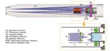
ObjectiveIn the inertial confinement fusion (ICF) implosion experiment, the 16.7 MeV deuterium-tritium (DT) fusion gammas provide a high-accuracy alternative to 14.1 MeV fusion neutrons for fusion reaction width and bangtime measurements. Gas Cherenkov detector (GCD) can be used to measure DT fusion gammas, which has the advantage of energy threshold to eliminate the interference of low-energy gamma photons. Previous studies mainly focus on optimizing system efficiency or time response of GCD. However, the system time delay and shield size of GCD are lacking in optimal design by simulation method. In the present study, we build a GCD simulation model using the Geant4 software, so as to optimize its structure considering the environment boundary of installation on the 100 kJ level laser facility. The influences of precursor signal and background interference on the fusion gamma measurement are analyzed. The GCD structure is optimized to increase the system sensitivity, and the system time delay and shield size are optimized to reduce the interference background. The measurement signal and performance changes of GCD are calculated by using the simulation model, which is helpful for configuring measurement parameters and estimating signal amplitude in implosion experiments conducted on the 100 kJ level laser facility.MethodsA whole three-dimensional model of GCD is built by using the Geant4 software, including the conversion processes of "gamma photon-Compton electron-Cherenkov photon" and the collection process of Cherenkov photons. First, the electron conversion efficiency changing with converter material and thickness is studied to obtain more high-energy electrons within a small emission angle. The Cherenkov photons arriving at the end of the gas cell are calculated according to the gas length and gas diameter, so as to optimize the structure of the CO2 gas cell. Meanwhile, the photon collection efficiency and the time waveform of collection photons are studied by changing the curvatures of the primary reflector R1 and the secondary reflector R2. Then, the influences of precursor signal and background interference on the main Cherenkov signal are analyzed, and the relationship between system time-delay tdelay (the peak time interval between the precursor signal and the main signal) and the distance from the secondary reflector to the first reflector L1 is calculated. Meanwhile, the tungsten shield size is determined by comparing the time waveforms of the collection Cherenkov photons before and after adding the tungsten shield. After that, the measurement signal of GCD installation on the 100 kJ level laser facility is calculated using the forward calculation method convoluting the collection Cherenkov photons, the impulse time response tIRF of photo multiplier tube (PMT), and the time spectrum tBW of fusion gamma emission. In addition, the detector sensitivity Sic (defined as collection Cherenkov photons per incident gamma photon on the convertor) and the system efficiency Sef (defined as collection Cherenkov photons per source gamma) are studied by changing the CO2 pressure and the installation distance.Results and DiscussionsAs the atomic number of material increases, the outcoming electrons within a small emission angle decrease (Fig. 3). A 15 mm thick carbon is selected as the gamma convertor according to the calculated electron conversion efficiency changing with the carbon thickness (Fig. 4). The CO2, as the radiation medium, is optimized as that with a length of 100 cm and a diameter of 15 cm according to calculated curve of collected Cherenkov photons (Fig. 5). The optimal curvatures of the primary reflector and the secondary reflector are chosen as 34 cm and 600 cm, respectively, according to the calculated collection photons and the signal frontier proportion χ (the ratio of collection photons at the 30 ps ahead of peak time to photons at the peak time) changing with R1 and R2 (Fig. 8). The intrinsic time response trp [full width at half maximum (FWHM) of temporal discretization of collection photons] is evaluated as about 16 ps, and χ is about 5.5% (Fig. 9). In order to minimize the influence of the precursor signal on the main Cherenkov signal, tdelay is optimized as 0.71 ns with L1 of 10.4 cm (Fig. 11). The diameter and length of the tungsten shield are chosen as 68 mm and 80 mm, respectively. The time waveform of the main Cherenkov signal has no change, while the precursor signal is significantly suppressed (Fig. 12). The amplitude of the simulated signal is about 0.7 V, while the neutron yield Yn is 1013 with the PMT gain M of 5×10³ and threshold energy Eth of 6 MeV (Fig. 14). The FWHM of the measured signal is about 164 ps after convoluting tIRF of 105 ps and tBW of 100 ps. In addition, Sic will increase by three orders of magnitude by increasing the CO2 pressure (Fig. 15), and it will decrease about 20% by changing the installation distance. Since the solid angle is inversely proportional to the square of the distance, Sef will decrease greatly (Fig. 16). In the implosion experiments with a higher yield, GCD can be installed farther to prevent PMT from outputting nonlinearly.ConclusionsA whole three-dimensional model of GCD is built by using the Geant4 software, including the processes of "gamma photon-Compton electron-Cherenkov photon" and the boundary processes of photon reflection and transmission. The gamma converter and the CO2 gas cell, as the radiation medium and the tungsten shield size, are optimized. A detector sensitivity of 0.21 photons per incident gamma photon and an intrinsic time response of 16 ps are achieved. The measurement signal and performance changes of GCD are calculated by using this simulation model, which is helpful for configuring measurement parameters and estimating signal amplitude in implosion experiments. The time response of GCD-coupled PMT can reach about 108 ps. The amplitude of the simulated signal is about 0.7 V, while the neutron yield is 1013 with a PMT gain of 5×10³ and a threshold energy of 6 MeV. The FWHM of the measured signal is about 164 ps after convoluting the fusion reaction width of 100 ps. The numerical calculation results indicate that the optimized GCD can meet the requirements of fusion gamma diagnostic in current implosion experiments on the 100 kJ level laser facility. In implosion experiments with high areal density, the instantaneous gammas activated by neutrons on the diagnostic devices will be strong. The influences of background interferences on the main Cherenkov signal are worth further study.
As a transition metal oxide, V2O5 has a moderate direct bandgap (2.2-2.8 eV), significant optical absorption characteristics in the visible light region, and excellent physical and chemical properties. It is considered a candidate material for excellent optoelectronic devices. Meanwhile, SnO2 is a common n-type semiconductor material with high electron mobility (240 cm2·V-1·s-1), which makes it a good electron transfer material with a low hole electron recombination rate and the ability to generate stable photocurrent. The nanofiber system exhibits sound crystallization, and the construction of specific functional heterojunctions can significantly enhance its performance, leading to its applicability in preparing high-performance optoelectronic detection devices. Therefore, photodetectors based on V2O5/SnO2 nanofiber heterostructures should theoretically have a faster light response speed than single component materials. To further investigate the optoelectronic properties of V2O5/SnO2 nanofiber heterostructures, we employ coaxial electrospinning technology to prepare V2O5/SnO2 nanofiber heterostructures with good crystallinity by adopting different vanadium and tin sources as precursors. Heat annealing treatment is carried out in different atmospheres to construct V2O5/SnO2 nanofiber heterojunctions with various morphology and sizes. By utilizing V2O5/SnO2 nanofiber heterostructures with varying morphology and sizes as a foundation, a high-speed optoelectronic detection device is constructed to assess its responsiveness to visible light in various laser irradiation conditions. We also elucidate the specific physical mechanism behind the rapid response to further expand the potential applications of V2O5/SnO2 nanofiber heterostructures.ObjectiveWith the rapid development of society, the demands for portable, lightweight, and large-area-compatible wearable electronic devices continue to grow, which drives photodetectors developing towards low-cost, high-performance, low-power, and large-scale manufacturing. One-dimensional inorganic nanomaterials facilitate the separation of electrons and holes due to their large specific surface area, high aspect ratio, abundant surface trap states, and unique electron confinement effects, thus extending the lifetime of photogenerated charge carriers. Additionally, the linear geometric structure provides sound elasticity to external stresses, making them less prone to cracking after deformation. These characteristics make one-dimensional inorganic nanomaterials an ideal choice for designing and preparing high-performance optoelectronic detection devices. In one-dimensional nanomaterial systems, nanofibers/wires have caught much attention from researchers in flexible display devices, gas sensors, and photodetectors due to their unique electrical and optical properties.Methods0.7993 g (0.003 mol) of acetylacetone vanadium oxide (C10H14O5V) is weighed and placed in a small beaker. Then a pipette is leveraged to measure 10 mL N, N-dimethylformamide (DMF), and the solution is dropped into a small beaker. Next, the beaker is sealed with aluminum foil and is placed in a heating magnetic stirrer of collector type constant temperature, with the temperature controlled at 75 ℃. Meanwhile, heating is conducted for 10 min to ensure complete dissolution. Subsequently, 1.1500 g polyacrylonitrile (10% PAN) is added to the dissolved C10H14O5V solution, placed in a heating magnetic stirrer of collector type constant temperature, and heated and stirred at 75 ℃ for 2.5 h to obtain a PAN+C10H14O5V shell solution with a certain viscosity. Later, 1.0607 g (0.003 mol) pentahydrate tin tetrachloride (SnCl4·5H2O) is weighed and placed in a small beaker. A pipette is adopted to measure 10 mL DMF, the solution is dropped into a small beaker, and then the beaker is sealed with aluminum foil and placed in a heating magnetic stirrer of collector type constant temperature. The temperature is controlled at 55 °C and heating is carried out for 10 min to ensure complete dissolution. 1.1730 g polyacrylonitrile (10% PAN) is added to the dissolved SnCl4·5H2O solution, placed in a heating magnetic stirrer of collector type constant temperature, and heated at 75 ℃ for 2.5 h to obtain a uniform PAN+ SnCl4·5H2O core solution. This experiment employs the MSK-NFES-1U electrospinning machine of Hefei Kejing Materials Technology Co., Ltd., with a 22G+17G coaxial stainless steel electrospinning needle, to spin (PAN+C10H14O5V)/(PAN+SnCl4·5H2O) coaxial nanofibers. Additionally, the two prepared solutions are injected into two syringes, with the shell solution connected to the outer tube of the coaxial needle and the core solution injected into the inner tube of the coaxial needle. The flow rates of the inner spinning solution and the outer spinning solution are adjusted to 0.5 mL/h and 0.8 mL/h respectively. By adopting the conditions including a voltage of 15.06 kV, a collection speed of 200.00 r/min, a moving speed of 5 mm/s, and a receiving distance of 20 cm, we successfully spin coaxial nanofibers composed of (PAN+acetophenoxy vanadium)/(PAN+stannic chloride pentahydrate). The spun original composite fibers are placed in an electric blast drying oven and dried at 90 ℃ for 8 h. Then the dried fibers are divided into two parts and placed separately in a high-temperature tubular sintering furnace. One part is annealed in an air atmosphere, and the other is annealed in an argon atmosphere. Both are kept at constant temperature for 1 h at 500 ℃, which leads to two V2O5/SnO2 nanofiber heterojunctions that are thermally annealed in different atmospheres.Results and DiscussionsAt room temperature, the photocurrent of V2O5/SnO2 nanofiber heterojunction devices is significantly enhanced under the presence of laser irradiation. Under the ultraviolet light irradiation with a wavelength of 405 nm and a power of 48 mW at a voltage of 2.0 V, the heterojunction exhibits 1.28 μA photocurrent, significantly higher than the dark current 0.96 μA at the same bias voltage [Fig. 7(a)]. In the same conditions, the photocurrent and dark current of pure V2O5 nanofiber devices are 0.43 μA and 0.41 μA respectively, with a difference of 0.02 μA between the photocurrent and dark current, which indicates there is no significant change between them [Fig. 7(b)]. Figure 8 shows the I-V curves of two types of photodetectors under different laser irradiation powers, with linear relations between photocurrent and bias voltage under different laser irradiation powers. As the power density of laser irradiation increases, the device photocurrent rapidly increases. In the same laser irradiation conditions, the photocurrent of V2O5/SnO2 nanofiber heterojunction photodetector is significantly higher than that of V2O5 nanofiber photodetector. With the periodic opening and closing of laser irradiation, the device photocurrent exhibits good repeatability corresponding to the periodic light illumination changes. During the observation period, there is almost no photocurrent attenuation, which demonstrates sound stability and photoelectric switching performance (Fig. 9). Under laser irradiation with a bias voltage of 3.0 V, a wavelength of 405 nm, and a power density of 123 mW, the optical switching ratio of the V2O5/SnO2 nanofiber heterojunction photodetector is 1.9, the responsivity is 3.97 A/W, and the specific detectivity is 2.2×10⁷ Jones [Fig. 9(a)]. Under laser irradiation with a bias voltage of 3.0 V, wavelength of 405 nm, and laser power of 123 mW, the response time and decay time of the V2O5/SnO2 nanofiber heterojunction photodetector are 0.556 s, while those of the V2O5 nanofiber photodetector are 1.39 s and 2.78 s respectively (Fig. 10). Obviously, after the combination of V2O5 and SnO2, the photocurrent response time and decay time are significantly improved.ConclusionsWe successfully prepare a V2O5/SnO2 nanofiber heterostructure using coaxial electrospinning technology. Based on this heterostructure, we design a photodetector and study the photoresponse performance of the V2O5/SnO2 nanofiber heterostructure photodetector in different lighting conditions. The experimental results show that under the modulation of a periodic laser with a bias voltage of 3.0 V, the V2O5/SnO2 nanofiber heterojunction photodetector exhibits fast optical response, with a response and decay time of 0.566 s, a responsivity of 3.97 A/W, and a specific detectivity of 2.2×10⁷ Jones. Meanwhile, the photodetector exhibits sound photoelectric detection performance at room temperature. The excellent performance is attributed to rapid and effective photo-generated exciton dissociation at the oxide heterojunction interface with type Ⅱ band alignment. Finally, our research can provide new ideas for the applications of oxide heterostructures in optoelectronic devices.
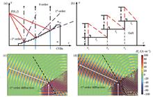
Results and discussion In the equivalent prism model, adding the blazed gratings significantly increases the energy proportion of the -1st order diffracted light, which proves the feasibility of the optimization mechanism (Fig. 1). The hollow grating lens decorated with the blazed structure can significantly increase the focal field energy with the peak value increasing to 2.91 times, while the focusing position is slightly shifted and the focusing width is broadened (Fig. 2). Under different preset focal lengths, the deflection of the beam passing through the lens varies, and the relationship between the focal field energy and the height of the blazed structure also changes. At near and medium focal lengths, the focal field energy first increases and then decreases with the height, and at far focal lengths, the focal field energy increases with the height (Fig. 3). When the number of blazed structures changes, more of them cause the diffracted beams to interact with each other, offset part of the phase difference, and reduce focal shift, with improved focusing energy efficiency (Fig. 4). The incident light distribution can also manipulate the focal field. By controlling the beam parameters to adjust the energy distribution of incident light in various regions of the grating, different diffraction efficiencies of regions are obtained, and the focusing field intensity is controlled (Fig. 5). According to the analysis of lens structural profile characteristics and diffraction mechanisms, when the proportion of incident light energy contributing to the first grating area of the lens is more than that of the second grating area, the grating diffraction efficiency is high and the electric field intensity increases with w0. When the contribution of incident light energy to the second grating area exceeds the first grating area, the grating diffraction efficiency decreases, and the electric field intensity becomes stable or even weakens with the rising w0 (Fig. 5). By utilizing the polarization independence of subwavelength grating lenses and adjusting the polarization composition of the incident field, solid single focus, "donut" shaped, "rocket" shaped, and "spindle" shaped focal fields can be obtained (Table 2).ObjectiveThe amplitude and polarization of cylindrical vector beams (CVBs) are distributed cylindrically and symmetrically, and the tight CVBs focusing plays an important role in optical micromanipulation, optical storage, laser micromachining, super-resolution imaging, particle acceleration, and other fields. At present, various focusing methods have been developed, such as traditional lenses, plasmonic lenses, negative refractive photonic crystal lenses, parabolic mirrors, and meta-lenses. However, there are limitations including diffraction limit, polarization dependence, and complex preparation. Subwavelength grating lens based on -1st order diffraction can achieve tight focusing of radial and azimuthal polarized lights spontaneously, breaking through the diffraction limit and realizing flexible focal field manipulation. Despite these advantages, the energy efficiency of its focal field still deserves further improvement. Therefore, we explore and propose a structural optimization scheme for a blazed subwavelength grating lens that can increase the energy ratio of -1st order diffracted light energy to enhance the focal field energy.MethodWe employ the full vector calculation of electromagnetic field (COMSOL Multiphysics software) based on the finite element method (FEM) to carry out specific research. The blazed structure is located on each grating step with a consistent height, and the overall lens structure is a uniform dielectric GaN. Firstly, an equivalent triangular prism model is built to verify the enhancement effect of the blazed structure on -1st order diffraction. Next, the energy and morphology changes of the focal field before and after modifying the blazed structure are compared, and the influence of the height, number, and location of blazed structures on the focal field is analyzed. Finally, the dynamic manipulation effect of the incident light amplitude distribution and polarization components on the focal field energy and morphology is studied.ConclusionWe propose a blazed subwavelength grating lens that can improve the diffraction efficiency of -1st order diffracted light and enhance the focal field energy of the negative refractive grating lens. As the preset focal length increases, the height of the blazed structure that satisfies the maximum diffraction efficiency of the lens also rises. The increasing number of blazed structures leads to more balanced energy of the outgoing beams in different regions and higher energy of the focal field. Meanwhile, the ability of the focal field to suppress the secondary focus is stronger, and the focal position is more accurate. By adjusting incident Gaussian radially polarized light, the dynamic control of the focal field energy is realized. Changing the polarization components of CVBs can also achieve lateral focusing modulation and obtain focal fields with diverse morphology. Finally, our study provides ideas for optimizing the focusing performance of subwavelength grating lenses and has potential applications in optical micromanipulation, super-resolution imaging, and other fields.
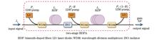
ObjectiveMulti-band transmission is considered an effective solution to address the increasing capacity constraints in fiber optic communication systems. However, due to the lack of mature optical amplifiers, the large-scale deployment of dense wavelength division multiplexing (DWDM) technology for long-distance transmission in bands such as O, E, and S has not yet been achieved. In recent years, researchers have discovered that different dopants in bismuth-doped silica fibers exhibit broad fluorescence characteristics in the near-infrared region. This finding brings hope for addressing the aforementioned challenges. In traditional approaches, the performance analysis of amplifiers often requires solving a set of coupled differential equations using methods such as the Runge-Kutta algorithm combined with the Shooting method or Relaxation method. When incorporating global optimization algorithms, it becomes necessary to solve thousands of related equations, resulting in a complex and time-consuming process. Previous research methods have mainly focused on the optimization design of Raman fiber amplifiers or hybrid optical amplifiers, with fewer studies specifically targeting the structural optimization design of doped fiber amplifiers, particularly bismuth-doped fiber amplifier (BDFA). Moreover, most of these studies have employed single-objective optimization algorithms, resulting in obtaining only one optimal solution at a time. In general, there is a trade-off relationship between the gain and noise performance of amplifiers. Increasing the gain often leads to the deterioration of the noise performance, and vice versa. As a result, there is no unique optimal solution. Therefore, it is necessary to design a method that can accurately model the amplifier and efficiently optimize multiple performance metrics simultaneously.MethodsThe backpropagation neural network (BPNN) is a type of multilayer feedforward neural network consisting of input layer, hidden layers, and output layer. The input layer contains six neurons corresponding to the input signal wavelength and five structural parameters of the amplifier. The output layer contains two neurons corresponding to the Gain and noise figure (NF) of the respective wavelength signals. The main characteristic of BPNN is the forward propagation of signals and the backward propagation of errors. It belongs to the supervised learning methods. For multi-objective problems, the objective values are typically mutually constrained, and there is no unique optimal solution. Using multi-objective optimization algorithms can provide a set of independent optimal solutions, allowing engineering designers to choose based on their actual needs. NSGA-II is a multi-objective optimization algorithm that improves upon the non-dominated sorting genetic algorithm (NSGA). By introducing fast non-dominated sorting, elite preservation strategy, and crowding distance operator, NSGA-II reduces computational complexity, improves optimization efficiency, and ensures the diversity of individuals in the population.Results and DiscussionsSimulation experiments were conducted using a theoretical model of a two-stage BDFA to obtain a sample set. The BPNN model was trained and tested with different sample sizes, with a training-to-testing set ratio of 9∶1. It was observed that as the sample set size increased, the overall trend of RMSE decreased while the R2 value increased (Fig.4). When the sample size reached 3000, the BPNN model achieved an RMSE of 0.191 for Gain and 0.084 for NF in the testing phase, with R2 values of 0.999 and 0.998, respectively. The established BPNN model exhibits high prediction accuracy and can effectively capture the nonlinear relationship between the structural parameters and performance of the two-stage BDFA. Based on the established BPNN model, the objective function is evaluated, and after 100 iterations, a Pareto optimal solution set containing 500 solutions is obtained (Fig.6). Furthermore, a comparison is made between the performance of using SVM and BPNN for predicting Gain and NF. The results show that the BPNN model has smaller prediction errors and higher accuracy in predicting Gain and NF. Additionally, the time required for optimization design using BPNN-NSGA-II is five orders of magnitude lower than using Relaxation method combined with NSGA-II, taking less than 80 seconds to complete the design. Compared to SVM-NSGA-II, the time is reduced by one order of magnitude (Fig.9).ConclusionsThis paper proposes a multi-objective optimization method that combines BPNN and NSGA-II algorithms for accurate modeling and efficient design optimization of two-stage BDFA. By establishing a BPNN model to map the nonlinear relationship between structural parameters and performance, it avoids the need for repetitive solving of coupled differential equations. After training and testing, the BPNN model exhibits low RMSE and high R2 values. Using this BPNN model in conjunction with the NSGA-II algorithm, a Pareto optimal solution set containing 500 solutions is obtained. The paper also provides the Gain and NF spectra for five different amplifier configurations. Compared to other methods, the proposed approach significantly reduces the optimization design time, improves optimization efficiency, and enables the simultaneous attainment of multiple optimal solutions, providing decision-makers with more choices.
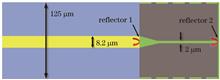
ObjectiveOptical fiber Fabry-Perot microcavity sensor has the advantages of small size and good stability, and it is widely used in the measurement of temperature, magnetic field, refractive index, and other physical quantities. However, the traditional processing method has many drawbacks and limitations. For example, the fusion method of single-mode fibers and special fibers may cause the fusion area to collapse and form a conical structure, resulting in poor performance of the prepared sensor; the operation of the hollow-core fiber filling method is difficult, and the preparation repeatability is poor; the chemical reagents of chemical corrosion method are easy to cause harm to the human body. The femtosecond laser two-photon polymerization 3D printing technology adopted in this paper has the advantages of high processing precision, strong flexibility, and high repeatability and can cope with more complex conditions to achieve structure preparation. In addition, the optical fiber Fabry-Perot microcavity sensor is widely used in refractive index sensing, but due to the introduction of a section of air optical path, its light conduction ability is relatively insufficient, and the insertion loss is large. In this paper, the optical micro-waveguide is introduced to form the integrated sensing and guiding optical fiber Fabry-Perot micro-waveguide cavity. The Fabry-Pert microcavity can limit the light field to the micron range and support and protect the micro-waveguide structure. Meanwhile, micro-waveguides not only ensure good optical conductivity of the structure but also further enhance the refractive index sensitivity of the overall structure based on their strong evanescent field characteristics.MethodsThe micro-waveguide Fabry-Perot cavity structure is designed by COMSOL and simulated by finite difference time domain method and finite element method. The simulation results show that the refractive index sensitivity of the proposed structure can reach 555.14 nm/RIU in the range of 1.333-1.337 (Fig. 3). The structure is prepared by femtosecond laser two-photon polymerization 3D printing after setting the printing parameters. First, the fiber coating layer is removed; the flat single-mode fiber core end face with a cutter is cut out, and it is cleaned with a welding machine. Second, the optical fiber is fixed to the printer position, and the lens is focused on the optical fiber end face. Third, the optical fiber end face is adjusted to the center position of the printing equipment for printing. Fourth, the structure is cured using propylene glycol methyl ether acetate solution and isopropyl alcohol solution (Fig. 4).Results and DiscussionsThe reflection spectrum of the printed structure in water is observed by the optical spectrum analyzer. It can be seen that the free spectrum range (FSR) of the structure formed in deionized water is 16.1 nm. The spectral Fourier transform results show that the structure forms a single peak with a good interference effect in the low-frequency band (Fig. 5). It is also confirmed that the micro-waveguide structure can play a good anti-interference role in the optical fiber structure and shield the external disturbance to a certain extent. The structures are placed in 12 sodium chloride solutions with different concentrations in the refractive index range of 1.3346-1.3764 for experiments, and the linear fitting results of the reflection spectra show that the sensing structure has good linearity and sensitivity of 525.81 nm/RIU in the refractive index range of 1.3346-1.3764 (Fig. 6 and Fig. 7). To verify the improvement effect of micro-waveguides on the sensing performance of Fabry-Perot microcavities, a waveguide free optical fiber Fabry-Perot microcavity with the same cavity length is prepared using 3D printing technology, and the structure is placed in different concentrations of sodium chloride solution in the refractive index range of 1.3346-1.3764; the linear fitting results show that the refractive index sensitivity of the microcavity structure without micro-waveguide is 115.31 nm/RIU. It is not difficult to see that with the support of a micro-waveguide, the refractive index sensitivity of the optical fiber Fabry-Perot microcavity has increased by nearly 4 times, and the peak interference spectrum has increased by 8.2 dB (Fig. 9).ConclusionsBased on femtosecond laser two-photon polymerization 3D printing technology, a novel optical fiber Fabry-Perot micro-waveguides cavity integrated sensing structure is prepared in this paper. By combining the stability spectrum of fiber Fabry-Perot micro-cavity and the strong evanescent field characteristics of the optical micro-waveguide, the refractive index parameter detection with high sensitivity is realized. In the refractive index range of 1.3346-1.3764, the sensitivity is 525.81 nm/RIU, which is 3.56 times higher than that of the waveguide-free Fabry-Perot microcavity, and the peak value of the generated interference spectrum is increased by 8.2 dB. Such a fiber optic sensor with a small sample size, high sensitivity, and good repeatability will undoubtedly become a powerful booster for the rapidly developing fiber optic sensing technology and biomedical research and has a wide range of academic research value and application prospects in biodetection-related fields.
ObjectiveDue to the advances in polarization-maintaining fiber technology, coil-winding process technology, and other optical fiber device technologies, high-precision fiber optic gyroscopes have been made possible for high-volume applications in navigation. However, in many unmanned vehicle platforms, the size, weight, power consumption, and cost control of the navigation system have high requirements, so it is not operable to suppress the temperature drift problem of fiber optic gyroscopes by adding a temperature control system. The fiber optic coil is the core component of the fiber optic gyroscope, but its preparation process requires the intervention of manual operation, resulting in a difference and poor consistency in product design and finished product, and its performance will deteriorate due to the external temperature perturbation. Although the development of low-temperature-sensitive optical fiber can improve the winding process to improve symmetry, optimize the cavity structure design, and slow down the rate of temperature perturbation to strengthen the gyroscope's self-suppressing ability of temperature drift, the gyroscope's temperature performance degradation caused by some human factors, device defects, and other factors is still unable to be effectively solved. Based on this, by relying on the fiber optic gyroscope system platform, we find the relationship between gyroscope output and temperature and other related factors and use algorithmic compensation to weaken thermally induced error effects of fiber optic gyroscopes. In this thesis, we start from the mechanism level and discuss and deduce in detail the deep-seated reasons for the deterioration of gyroscope performance due to the phase error caused by the temperature influence of the fiber optic coil, which is the core component of the fiber optic gyroscope, and we carry out the process correlation analysis of the influence of the temperature factors and put forward a new type of zero-drift polynomial temperature compensation model that can be realized in an engineered way. The proposed compensation scheme based on this model is verified to be effective and can significantly suppress the gyroscope temperature drift error.MethodsThrough the fiber optic gyroscope temperature drift profiling derivation, the deep-seated causes of gyroscope drift error caused by temperature perturbation are analyzed, and the correlation of each temperature term influence factor with the actual output of fiber optic gyroscope is verified by combining with the process correlation theory. It is found that a temperature sensor can only characterize two temperature factors, temperature and temperature variation rate, but not the temperature gradient factor. Simulation analysis based on the process correlation theory shows that the compensation effect can be improved by introducing the temperature gradient factor under variable temperature conditions. In view of the fiber material properties, when the temperature changes, it will cause the material properties to change. Through simulation analysis, it is found that the output of the fiber optic gyroscope is correlated with the coupling factors of the product of temperature, temperature variation rate, and temperature gradient under variable temperatures. Finally, based on the relevant theoretical analysis, a temperature compensation algorithm model is established by simultaneously considering the temperature, temperature variation rate, temperature gradient, and the product of the three factors, and the validity of the model is verified through experiments.Results and DiscussionsThrough theoretical analysis, it is found that the fiber optic gyroscope cannot characterize the temperature gradient factor with the help of only one temperature sensor. Therefore, an implementation method of adding two temperature sensors inside the fiber optic gyroscope is proposed (Fig. 4). Simulation analysis with the help of process correlation theory (Fig. 6) reveals that there is indeed a correlation between the output of the fiber optic gyroscope and the temperature gradient factor during the temperature change process, which further supports the accuracy of the aforementioned theoretical analysis. Therefore, the temperature gradient factor is introduced when the compensation model is established. Through the offline comparison simulation test, it is concluded that the compensation model considering the temperature gradient factor can further improve the accuracy of the compensation model and enhance the gyroscope temperature performance (Fig. 7). In addition, by further analyzing the mechanism of thermally induced error in fiber optic gyroscope and verifying it with the help of process correlation theory simulation, a more comprehensive compensation model (Eq. 12) is proposed by simultaneously considering the temperature factor, the temperature variation rate factor, the temperature gradient factor, and the coupling term of the product of the three factors. Finally, the new temperature compensation model is verified to be more accurate and better compensated by means of multi-sample experiments (Fig. 11).ConclusionsIn this paper, a new multinomial algorithm compensation model is proposed, which simultaneously considers the temperature factor, the temperature variation rate factor, the temperature gradient factor, and the coupling term of the product of the three factors. We combine the analysis of thermally induced error mechanism derivation and process correlation theory as the designation idea and analyze the temperature compensation algorithm model of fiber optic gyroscopes. The feasibility of the algorithm is verified through offline compensation, and the zero-bias stability accuracy of the gyroscope after compensation is significantly improved compared with the compensation algorithm that only considers three factors, namely, temperature factor, temperature variation rate, and temperature gradient. In addition, the compensation parameters are burned into the gyroscope by means of multi-sample experiments, and the full variable temperature experiments are carried out under variable temperature conditions (-40-65 ℃, 1 ℃/min) for verification. The experimental results show that under the variable temperature conditions, the zerobias stability of the three fiber optic gyroscope samples is better than 0.005 (°)/h (100 s smoothing), and the compensation effect reaches the expected effect. Due to the variability of the fiber optic gyroscope, the next step is to verify the effectiveness of the algorithm through large-volume experiments.
ObjectiveInterferometric fiber optic hydrophone is a relatively mature solution in the current fiber optic hydrophone system and features high sensitivity, large dynamic range, strong anti-interference ability, and easy array formation. Meanwhile, it is suitable for underwater targets and is widely employed in fields such as detection and underwater energy exploration. In recent years, the application scenarios of fiber optic hydrophones have gradually developed into complex scenarios such as far-reaching seawater acoustic detection and mobile platform deployment. These scenarios pose more challenges to the signal detection performance and noise stability of hydrophones. Phase-generated carrier (PGC) demodulation is a commonly adopted signal detection method for interferometric fiber optic hydrophones. Since the operating point and carrier modulation depth are greatly affected by external environmental changes, the PGC demodulation system has unstable output phase signals. In particular, the system's self-noise stability fluctuates greatly with environmental changes. This problem has become an important factor limiting the performance of fiber optic hydrophone systems.MethodsCentering on the noise stability of interferometric fiber optic hydrophones based on PGC demodulation, we build a noise transfer model of the interferometric fiber optic hydrophone based on PGC demodulation and focus on analyzing changes in the two parameters of the carrier modulation depth and operating point. Meanwhile, the mechanism of influence on the stability of PGC demodulation noise is studied. A new multi-phase PGC demodulation scheme is proposed, where a 3×3 coupler is introduced into the traditional PGC demodulation architecture for multi-phase detection, and the three interference signals are fused by phase shift characteristics of the coupler. The multi-phase PGC demodulation algorithm performs PGC demodulation on the outputs of three 3×3 couplers respectively, and then averages the demodulation results of the three channels. Since the measured phase signals in the three demodulated output signals are the same, the averaging operation has no effect on them, while the noise signals can be suppressed. Additionally, as the initial phases of the three interference signals differ by 2π/3, the noise influence exerted by the initial phase changes can be minimized by averaging regardless of whether the working point of the interference signals changes or not. Therefore, the demodulation noise can be relatively stable. As the working point of the hydrophone changes, this scheme can reduce fluctuations in the noise transfer coefficient of the light source intensity noise.Results and DiscussionsWe conduct simulation experiments to verify the performance of the multi-phase PGC demodulation algorithm. The simulation results show that sound noise stability can be achieved under different carrier modulation depth (C) values. Under different C values, the fluctuation of the noise transfer coefficient is less than 0.5 dB, and compared with the traditional PGC demodulation algorithm, the stability of demodulation noise of multi-phase PGC demodulation algorithm is significantly improved (Figs. 3 and 4). A multi-phase PGC demodulation system based on 3×3 coupler is built, and the demodulation phase noise performance of the system is experimentally verified. A multi-channel synchronous sampling analog-to-digital converter (ADC) is employed to acquire the three outputs of the coupler. The traditional PGC demodulation method and the multi-phase PGC demodulation algorithm are utilized to demodulate the original data collected by the system. Additionally, we calculate the noise spectrum levels of the demodulated signals of the two methods at 1 kHz frequency separately and analyze the noise fluctuation characteristics of the system. The experimental results show that the self-noise fluctuation obtained by demodulating the three outputs of the 3×3 coupler using the traditional PGC demodulation method is greater than 4.5 dB (Fig. 6). The noise spectrum levels obtained by the multi-phase PGC demodulation method are significantly reduced, and the noise fluctuation during the entire test cycle is less than 1.8 dB (Fig. 6). The experimental results verify the effectiveness of the multi-phase PGC demodulation algorithm.ConclusionsWe build a noise transfer model for interferometric fiber optic hydrophones, analyze and derive the noise transfer model of system noise sources on demodulation results, and propose a multi-phase PGC demodulation algorithm. Compared with traditional PGC demodulation algorithm, the proposed algorithm can suppress the fluctuation of light intensity noise transfer coefficient under the changing operating point, and improve the noise stability of demodulation results. Simulation and experimental results are consistent with the theoretical analysis results of the model. In applications such as deep-sea exploration and long-distance target detection which have increasingly stringent noise performance requirements for fiber optic hydrophones, the noise transfer model and the multi-phase PGC demodulation algorithm based on 3×3 coupler proposed in our study have research and practical significance.
ObjectiveThis study aims to develop compact and lightweight imaging optical structures, transcending the challenges posed by intricate architectures, specialized materials, and unique surface configurations prevalent in traditional optical design paradigms. In response to these challenges, we introduce computational imaging techniques, seamlessly integrating the realms of optical design and image restoration. This integration alleviates the intricacies associated with front-end optical system design while concurrently streamlining the process through the application of image restoration algorithms. By transposing the complexities of optical design into the algorithmic realm, we endeavor to reduce optical system complexity while preserving image quality.MethodsWe propose an end-to-end (E2E) framework to facilitate the creation of the diffractive optical element (DOE) capable of extending the depth of field (DOF). This framework integrates point spread function (PSF) design, imaging models, and deep image restoration networks through the utilization of modern deep learning tools. As a significant departure from traditional practices, this framework eradicates the traditional segregation between front-end optical design and back-end image processing stages. This method uses image quality as the final evaluation criterion to find the optimal balance between the consistency of a given DOF range and PSF. Moreover, the holistic E2E approach introduced by this method encompasses the intricate task of designing lenses (or lens groups) to accomplish the focus function. This strategic integration effectively simplifies the design complexities intrinsic to DOE, steering the design focus exclusively toward extending the DOF. Specifically, we employ the phase coefficients of cubic phase plates and the one-dimensional height map of rotationally symmetric DOEs to facilitate the dimension reduction of optical design parameters. Network constraints encompass the L1 constraint as the loss function for the image, alongside the inclusion of PSF consistency at varying depths as a specialized constraint for large DOF design. The amalgamation of these constraints gives rise to the loss function for the E2E network, propelling the designed network toward optimization updates. To enhance the network's generalization capabilities, the proposed method undergoes alternating training on two datasets: the FlyingThings 3D dataset, containing 21818 training images and 4248 test images, and the DualPixel dataset, featuring 2506 training images and 684 test images. This dual dataset training regimen yields designs for optical components and culminates in the final imaging outcomes.Results and DiscussionsThe efficacy of the proposed large DOF optical model is robustly validated through comparative analysis with Zemax results, visually depicted in Fig. 4. Subsequently, the E2E approach is efficaciously applied to the design of large DOF imaging systems, encompassing the design of both rotationally symmetric DOEs and cubic phase plate, depicted through their respective height maps in Fig. 5. To provide a comprehensive portrayal of the DOF extension effects within varying scenes, Fig. 6 presents the imaging quality of diverse DOF extension methods across different defocus levels, incorporating images from both the FlyingThings 3D and DualPixel datasets. Additionally, Fig. 7 effectively captures the graphs detailing variations in PSNR and SSIM concerning distinct DOF extension methods over the test dataset, showcasing the relative stability of imaging quality changes within a smaller defocus range for cubic phase plates. However, they experience performance degradation under more pronounced defocus levels, particularly evident in the real-image context of the DualPixel dataset, where rotationally symmetric DOEs outperform cubic phase plates. In contrast, the rotationally symmetric DOEs consistently maintain high image quality both at the focal point and under larger defocus levels. Furthermore, we underscore the robustness of the design method by meticulously validating its performance using non-design values within defocus ranges, as exhaustively detailed in Table 1. Empirical evidence derived from these experiments unequivocally demonstrates that E2E-optimized rotationally symmetric DOEs and cubic phase plates effectively elevate image quality within the defocus range of [-30, 30].ConclusionsIn summary, we introduce an E2E optical design method based on computational imaging. The overall design workflow and performance of DOE are successfully enhanced by constructing a comprehensive model that integrates two different domains, optical design, and image restoration and applying the idea of global optimization with image quality as the final evaluation criterion. The method reduces the requirement for imaging quality of the front-end optical system and eliminates residual aberrations using image restoration algorithms, thus realizing a compromise between optical design and image algorithms. The method covers key aspects of optical field propagation, detector noise, and image post-processing. By building the corresponding models and jointly optimizing the optical models and image algorithms with the modern deep learning models, we successfully design lightweight and thin DOEs suitable for extended DOF and achieve high-quality imaging in a simple optical system with significant DOEs. In conclusion, this research advances an E2E optical design method rooted in computational imaging, enhancing the design of DOEs for extended DOF. The implications of this work extend to the broader field of computational optical imaging, holding both theoretical and practical significance.
ObjectiveGhost imaging has emerged as a promising technique, which is characterized by mitigating the adverse effects of atmospheric turbulence and scattering media, and has the potential to surpass the diffraction limitations. Meanwhile, its potential applications in remote sensing are highly anticipated. However, effective evaluation methods that can quantitatively assess the influence of various components within the imaging system on its performance should be proposed to facilitate the practical implementation of ghost imaging. Such methods can provide valuable support for the design and optimization of imaging systems. Currently, one area of research focuses on evaluating the influence of the observation matrix. Although commonly adopted evaluation methods that rely heavily on specific imaging scenarios and reconstructed images can accurately characterize the effect of the observation matrix based on image quality after reconstruction, they often fall short of independently assessing the system's overall performance. Therefore, it is essential to put forward a quantitative evaluation method prior to the reconstruction stages. Studies have indicated that information theory-based approaches hold promise in achieving this objective. Some researchers have evaluated the influence of factors such as the row number or the distribution type of the observation matrix on system performance by calculating the mutual information between signals received by bucket detectors and imaging scenes. Despite favorable results yielded by their methods, they encounter challenges such as difficulty in acquiring prior information or limited applicability. To this end, we explore a novel method for evaluating the performance of ghost imaging systems before the reconstruction process. This method employs communication system channel evaluation techniques to analyze and assess the observation matrix. By treating the observation matrix as a channel matrix, we derive the channel capacity of the sampling system and utilize it to evaluate the influence of the observation matrix on the system performance. Consequently, this approach addresses the limitations identified in previous studies.MethodsFirstly, we establish an analogy between the ghost imaging system and the communication system, where the imaging scene information is considered as the information source, the M times sampling process as the channel, and the received signal of the bucket detector as the sink. At this juncture, the observation matrix assumes the role of the channel matrix, which constitutes a crucial component of the channel and can be analyzed by the channel evaluation method employed in communication systems. Subsequently, the M×N channels represented by the observation matrix undergo singular value decomposition, yielding R independent subchannels. Given that the interference during ghost imaging sampling primarily manifests as Gaussian white noise, we assume the channel to be a Gaussian channel. Consequently, the channel capacity of each subchannel can be determined by employing the formula for Gaussian channel capacity. The signal power during the sampling corresponds to that of the imaging scene information. Compared to temporal variations of the imaging scenes, the duration required for the M times sampling is relatively short. Thus, it is reasonable to assume that the overall power of the imaging scene information remains constant throughout the sampling. On the other hand, the noise power corresponds to the average power of Gaussian white noise, which is numerically equivalent to its variance. By substituting the signal power and noise power of each subchannel into the formula for Gaussian channel capacity and aggregating the results, we can obtain the total channel capacity of the ghost imaging sampling. Furthermore, the Bernoulli inequality is applied to establish a lower bound on the channel capacity value, and an approximate representation is employed. On this basis, we observe that the component associated with the signal power and noise power remains constant and nullifies during comparing the channel capacity of different observation matrices. Consequently, in practical applications, it is unnecessary to measure the total power of the imaging scene information and the average power of the Gaussian noise.Results and DiscussionsBased on the imaging simulation test encompassing 100 diverse imaging scenes, 20 distinct types of observation matrices, and 2 reconstruction algorithms, a comprehensive analysis is conducted by comparing the test results with the evaluation outcomes of image quality following imaging reconstruction. The findings indicate strong consistency between the effectiveness of our study in evaluating system performance before imaging and the validation results obtained by post-imaging. An imaging scene is selected, and the channel capacity variations for the sampling process and the MSE for reconstructed images are compared with the type of matrix element distribution. Then, it is evident that both exhibit identical dependence on the type of matrix element distribution at the same sampling ratio (Fig. 6). This consistency is observed in all imaging scenes. Additionally, by simulating the imaging process using a Bernoulli distribution matrix (p0=0.001) for a selected imaging scene, it is observed that the normalized channel capacity curve of the sampling process and the normalized inverse MSE curves of the reconstructed exhibit a high concordance degree, with R2 of 0.97606 and 0.95878 (Fig. 8). In the case of extending the imaging and fitting process to all 100 imaging scenes, it becomes apparent that the R2 values for the two reconstruction algorithms generally exceed 0.8 (Fig. 9).ConclusionsThe incorporation of information theory in this method facilitates an objective assessment of the transmission capability of the observation matrix for imaging scene information by utilizing the channel capacity of the sampling system. This approach enables independent and effective evaluation of system performance, disentangled from prior knowledge of the imaging scenes or reconstructed imaging results. The evaluation outcomes demonstrate robust consistency with the validation results obtained by post-imaging. Under constant sampling ratio, the mean squared error (MSE) of the reconstructed images and the channel capacity exhibit parallel dependency on the distribution type of matrix elements. Similarly, when the distribution type of matrix elements remains the same, the curves depicting the normalized channel capacity and the normalized inverse MSE as functions of the sampling times present a high concordance degree, with R2 values generally exceeding 0.8. Moreover, the simulation verification encompassing a diverse range of imaging scenes and observation matrices yields sound results. This further proves the applicability of the proposed method across various scales of imaging scenes and different types of ghost imaging systems, making it highly suitable for widespread implementation in common remote sensing scenarios.
ObjectiveBroad-spectrum optical systems have superior performance. They can obtain more comprehensive and accurate target information and are conducive to enhancing the detection and identification capabilities of optoelectronic equipment. In addition, they have an irreplaceable role in complex environments. However, their design is often difficult, and the current main optical design method is to optimize the selected initial structure, but the initial structure of the broad-spectrum optical system is inefficiently constructed. Therefore, the design cycle is long, and it relies too much on the experience of the designers. In this paper, we explore the design method of broad-spectrum optical systems, analyze the system's confocal and co-image plane conditions from the theoretical level, and focus on the initial structure construction method of broad-spectrum systems based on a genetic algorithm.MethodsFirstly, a multi-band equal focus method based on optical focus matching is proposed to derive the equal optical focus condition by taking a system with two bands and two optical groups as an example, and the system's focal lengths in each band are set to be equal by reasonably allocating the optical focus of each optical group. Then, in order to meet the different wavelengths of the common image plane imaging, the geometric optics formula recursively obtains the combined system of equal image plane conditions. The idea of a genetic algorithm is used to independently construct the optical group composition and structure form of the broad-spectrum optical system and iteratively solve the optimal initial structure, and the selection of the optimal group is based on the experience of the designers, which is mainly considered in the differences in the focal lengths of different wavelengths, the differences in the position of the imaging surface, the distribution of the optical focal lengths, the ratio of the lens diameter to thickness, and the thickness of the edge of the lens, and other aspects. Finally, the selected optimal initial structure is optimized to obtain a broad-spectrum optical system with a small number of lenses, small volume, light weight, and good imaging quality.Results and DiscussionsFor the same target, different focal lengths will lead to differences in the position and size of the image, and with the broadening of the spectral range, the imaging differences increase, which will seriously reduce the imaging quality of the system. The theoretical derivation of this paper obtains the conditions of equal focal lengths and co-image surfaces, which can solve this problem. For the optimal initial structure construction of the transmissive system, this paper independently constructs the optical group composition and structural form of the system by genetic algorithm, while the existing papers use optimization algorithms for the design of reflective systems, such as the design of reflective free-form surfaces. In the initial structure construction process of such systems, the parameters of the incident light and the requirements of the outgoing light are determined, and the algorithm process actually fits the reflective surface according to the laws of geometrical optics under the premise of known incident and outgoing light. In contrast, the transmissive system contains multiple optical groups; the light propagation path inside the system is completely uncertain, and the number of optical groups and the structure form are all unknown. Therefore, the main framework strategy and process of the broad-spectrum initial structure construction algorithm in this paper are completely different. In addition, we generate many possible optimal solution results through the powerful computational ability of the algorithm, which ensures a high probability of occurrence of the optimal solution by the number and effectively prevents the algorithm from falling into the local optimum. The results of the algorithm (Fig. 3) indicate that it can efficiently generate a large number of excellent initial structures of the broad-spectrum system, providing training samples for the later AI-based optical system design.ConclusionsIn this paper, we derive the broad-spectrum co-focal distance and co-image plane equations, determine the focal distance difference and image plane difference fitness function, and establish the genetic algorithm structure parameter variation and material crossover method. In order to verify the feasibility and efficiency of the method, a visible and near-infrared broad-spectrum optical system is designed, and the system has an imaging band of 0.4–1.2 μm and a focal length of 40 mm. The difference in the focal length within the range of the band is less than 0.03 mm, and the imaging quality is good in the broad-spectrum range. The design results show that the genetic algorithm-based broad-spectrum optical system construction method can generate 1024 excellent populations at a time, of which 407 iterative individuals can meet the requirements of the objective function. The appropriate optimal solution is input into the Zemax software for optimization, and a broad-spectrum optical system that meets the requirements can be obtained very quickly. In summary, the proposed genetic algorithm can shorten the design cycle and improve the design efficiency of broad-spectrum optical systems.
ObjectiveAs a form of passive cooling, radiative cooling can reduce the temperature of objects below the ambient temperature without additional energy consumption, and has become a research hotspot in thermal management in recent years. Daytime radiative cooling has been achieved by radiating out heat through the atmospheric transparent window (ATW, 8-13 μm) and simultaneously reflecting incident sunlight to avoid heating, which has been employed in green buildings, solar cells, and other fields. Generally, the physical quantities that measure the cooling material performance are temperature difference and radiative cooling power. Compared to the variability value of temperature differences measured under different circumstances (e.g., locations, atmospheric temperatures), the radiative cooling power is stable and can reflect the cooling performance more objectively. However, there are no specialized instruments measuring the radiative cooling power, especially those compatible with various materials with different cooling capabilities, which has become an obstacle to standardized radiative cooling evaluation. Therefore, we design a kind of measurement device for measuring radiative cooling power, and hope to provide a helpful tool for the material development and large-scale applications of radiative cooling technology.MethodsAccording to the thermal balance principle, we design a cooling power measurement system consisting of a single-chip microcomputer as the control unit, a DS18B20 digital temperature sensor and a platinum resistance of PT100 as the temperature sensor, and a positive temperature coefficient heater as the executive source. The temperature sensors measure the ambient temperature and surface temperature of the sample to be tested and transfer the data to the controller in the form of SPI communication and 1-wire bus communication. Thus, the temperature differences and their changing rates can be obtained. In data processing, we adopt the idea of fuzzy control. First, we finish the value fuzzification about temperature differences and their changing rates, and then determine the membership functions. After the fuzzy inference process, we leverage gravity method to defuzzify and obtain accurate control quantity. On this basis, the fuzzy proportional-integral-derivative (PID) control algorithm is utilized to output pulse width modulation waves with different duty cycles, and then adjust the effective voltage value and working power on the PTC. Then, we control the temperature of radiative cooling materials to be consistent with ambient temperature and finally calculate the radiative cooling power based on the electric power consumption. Additionally, we design a CAD model and fabricate the mechanical structure by empoloying the 3D printing process.Results and DiscussionsRadiative cooling is a surface cooling technology with zero energy consumption. During the measurement, cooling materials initially achieve a ambient temperature drop due to thermal emissions, and then can be heated and maintain consistency with the ambient temperature under the action of the PTC heater. Meanwhile, we adopt the effective voltage changes of the PTC as input and the temperature change of the sample material as output. After Laplace transformation, we can obtain the system's transfer function. On this basis, we develop a simulation model for a fuzzy PID controller (Fig. 9), which realizes higher-accuracy temperature control and enhances the system's anti-interference capability (Fig. 10). Traditional PID control cannot meet the accuracy requirements of temperature control when dealing with cooling materials with different cooling performance, which is because the steady-state errors will occur under the unchanged parameters. The employed fuzzy PID control algorithm can adaptively change the PID parameters according to the values and changing rates of the temperature differences returned from different materials. Additionally, it can adjust the controller which outputs multiple PWM waves without interfering with each other to meet the testing requirements of various radiative cooling materials. The outdoor test results show that the homemade PVDF films of different thicknesses achieve cooling temperatures of 5.7 ℃ and 7.0 ℃ respectively in the evenfall (Fig. 13). After adopting the fuzzy PID controller, the system achieves the ideal results with no overshoot, and the steady-state error remains within 0.1 ℃ (Fig. 14). We also obtain the actual cooling power. The calculation results show that the cooling power values are 53.33 W/m2 and 67.45 W/m2 respectively. The measured cooling power maintains the same trend as the theoretical prediction.ConclusionsWe design a radiative cooling power measurement system based on the fuzzy PID control algorithm by employing the STM32F103 chip as the main controller. From the component point of view, since the core components of the system are only the main controller, temperature sensor, and PTC heater, the system is simplified from the number of hardware and device complexity. Meanwhile, the system meets the power measurement requirements of different radiative cooling materials based on a fuzzy PID control algorithm. In the simulation model, the system shows excellent stability and anti-interference capability. The actual outdoor test results indicate that an ideal temperature control effect can be yielded for different materials, and the control accuracy after stabilization can reach ±0.1 ℃. On this basis, the system initially realizes the miniaturization and practical applications of the measuring device, with promising application prospects.
ObjectiveT-type theodolite is widely used in various test tasks due to its large measurement range, non-contact feature, high measurement accuracy, replaceable load sensor, and availability for multi-sensor sharing. The T-type theodolite has a load-carrying structure. For different test environments, different load imaging components can be installed on its side axis to reach the measurement purpose. However, after replacing the imaging detection sensor, the projection center of the optical imaging system and the position relationship between the imaging optical axis and the alignment axis of the T-type photoelectric theodolite will be changed. These factors will lead to angle deviation of the T-type photoelectric theodolite in the measurement. Therefore, the triple difference and the projection center coordinates of the T-type theodolite need to be calculated and eliminated. For the study of photoelectric theodolite, there is a lack of effective methods to simultaneously detect the projection center and triple difference. Therefore, a simple method of measuring the triple difference of T-type photoelectric theodolites is proposed in this paper. The photoelectric theodolite imaging system collects images of the near and far station poles respectively. Then, the projection center coordinates of the imaging optical system can be calculated from the image coordinates of the poles, the intrinsic parameters of the imaging system, and the encoder value of the photoelectric theodolite, thereby achieving the detection of optical axis parallelism.MethodsFirstly, the projection equation between a point in the geodetic coordinate system and the image point on the camera image plane is derived by combining the transformation relationship of the related coordinate system [Fig. 1(a)] and the camera's pinhole imaging model [Fig. 1(b)], as well as the triple difference of the photoelectric theodolite. Secondly, the projection coordinates of the station pole vertex on the image plane are obtained according to the positive and reversed images of the photoelectric theodolite, and the imaging projection relationship combining the projection center and the triple difference is derived. The influence of the translation vector and triple difference on the miss distance of the projection point of the station pole vertex on the imaging plane is analyzed, and the projection center coordinates and triple difference of the system are calculated. Then, the optical axis parallelism of the photoelectric theodolite is detected. Finally, simulations and practical experiment results show that the proposed method is effective.Results and DiscussionsExperimental results (Table 1) show the projection center coordinate values and triple difference values obtained by linear calculation according to the proposed algorithm. Before optimization, the average of the reprojection errors is calculated, which is 0.7321 pixel in the horizontal direction and 0.7146 pixel in the vertical direction [Fig. 10 (a)]. After Levenberg-Marquadt optimization, the average of the reprojection errors in the horizontal direction is 0.2744 pixel, and that in the vertical direction is 0.2287 pixel [Fig. 10 (b)]. Therefore, it can be concluded that the accuracy after optimization has been improved by about 65%, which further verifies the effectiveness and correctness of the proposed detection method.ConclusionsIn this paper, the projection equation between a point in the world coordinate system and an image point on the camera image plane is derived by combining the pinhole imaging model and the triple difference of the T-type photoelectric theodolite, which can be applied to the nonlinear optimization of the photoelectric theodolite imaging system in the shooting range. Then, the calculation method of the projection center coordinate and the trilateration is derived, and a method is proposed to detect the projection center and the trilateration of the optical axis parallelism simultaneously with only two station poles, and the detailed algorithm flow chart is given. The experimental results show that the reprojection error of the system is less than 0.3 pixel, which proves that the method proposed in this paper can effectively solve the detection problem of projection center and optical axis parallelism triple difference in T-type photoelectric theodolites. However, this method is not sensitive to small-range changes of tx, so how to accurately and efficiently calculate tx to further improve the detection accuracy of the system is a problem that needs further research in the future. In addition, in the actual experiments, we only evaluate the reprojection errors and do not apply the detection results to the final theodolite measurement, especially for experimental measurements at high elevation angles (greater than 65°). This is the content that needs further experiments in the future.
ObjectiveStructured light vision is an optical 3D surface measurement technology, which features fast speed, high precision, and strong robustness. The traditional optical plane model theory generally regards the projection plane of line structured light as the ideal plane to determine spatial parameters of the optical plane. However, the distortion in the lens of the structured light emitter causes the light plane to bend. Therefore, in the traditional methods, the structured light emitter must be accurately calibrated to avoid nonlinear effects. Due to system assembly errors and complex calibration processes, it is difficult to convert the distorted optical surface into an ideal optical plane just by accurate calibration. The surface bending of line structured light should be fully considered to achieve high-precision line structured cursor setting under a large field of view.MethodsTo avoid the influence of lens distortion on calibration accuracy, we propose a new method for surface calibration of linear structured light based on building a surface grid model. First, the camera rays are tracked along the horizontal and vertical directions of the image respectively, and then the intersection depth between the camera rays and the optical surface can be converted into linear changes of the sub-pixel column coordinates or row coordinates of the optical fringe image respectively. The space line structured light surface is decomposed into multiple curves. Then, the grid points formed by the intersection of horizontal and vertical curves are fitted by an equal almost weighting method to obtain the surface grid of line structured light. The fitted surface grid of linear structured light corresponds to the pixel grid for ray-tracing in the image. Since the local surface of linear structured light can be regarded as a plane after differentiation, the center point of any sub-pixel light strip of non-image pixel grid points can be reconstructed in 3D by establishing the homologous relationship between pixel grid points and surface grid points.Results and DiscussionsBy analyzing the computational cost of polynomials of different orders and the fitting accuracy of sample points, the optimal fitting order for ray-tracing is determined (Table 2). To analyze the algorithm robustness, we compare the calibration accuracy of the algorithm and the tracking range of rays under different numbers of calibration images (Table 3). Additionally, the comprehensive analysis and verification show that the proposed method improves the applicability of the calibration method to the distribution directions of down-line structured light in different scenes. By adding different noise levels to the calibrated images, the algorithm is verified to have sound anti-noise performance (Tables 4 and 5). The distance measurement error for any adjacent target with a distance of 55.00 mm is less than 0.08 mm, and the distance measurement accuracy for adjacent targets with a distance of 1133.85 mm can reach 0.50 mm (Table 7). The dimensional measurement accuracy of the 880 mm×715 mm standard body is higher (Table 8), which verifies that the proposed method has significant advantages in large-field dimensional measurement.ConclusionsA new calibration method based on ray-tracing for surface grids of linear structured light is proposed. Since the lens distortion of the linear structured light emitter is unavoidable, the plane of the linear structured light is distorted into a light surface. To reduce the influence of optical plane distortion on calibration accuracy, for each optical plane in finite space, we simplify the distorted optical surface to multiple curves in space based on the ray-tracing model. Meanwhile, we build a surface grid model of linear structured light based on the principle of equal probability weighting and combine the bidirectional ray-tracing to realize the calibration of any distribution of linear structured light. Additionally, the high-precision reconstruction of the sub-pixel coordinates of the center point of the light strip is realized by employing the homologous relationship between the surface grid points of the linear structured light and the pixel grid points of the image.
ObjectiveThe developing modern economy and manufacturing industry have put forward a higher demand for related measuring instruments. However, the requirements for orthogonality of internal structures increase the difficulty of instrument manufacturing, and the production efficiency is reduced. To break through the limitations in the production and manufacturing of large-scale measuring instruments in China, the concept of non-orthogonal shafting measuring instruments is proposed. This kind of instrument does not require the shafting to be perpendicular or intersecting with each other, and the non-orthogonal shafting laser theodolite (N-theodolite) is a typical non-orthogonal shafting instrument. Much research has explored its measurement performance and related theories. However, due to the lack of the reference end on the laser axis for a single N-theodolite, the inverse kinematics model fails to be established accurately. The inverse kinematics model is necessary for precision theory research, which is convenient for data simulation of error spatial distribution. Besides, the guidance technology based on the inverse model can help improve the automatic measurement function of the N-theodolite. Therefore, to address the difficulty of calculating the rotation angle for the N-theodolite in inverse motion without a reference end, the linear model for the inverse motion to achieve fast and high-precision calculation of the rotation angle is proposed in this paper.MethodIn this paper, the basic theory of Lie groups and Lie algebras is introduced to achieve fast and high-precision calculation of the rotation angle. First, based on the theory of Lie groups and Lie algebras, the kinematics model of the N-theodolite can be constructed. The coordinate transformation matrix is represented as the product of the exponentials formula (POE) with clear physical meanings. Second, the error model of N-theodolite can be obtained through the corresponding differential calculations, and the parts related to the rotation angle error component are preserved. Then, the constraint relationship between the spatial target point and the laser axis pose parameters is constructed, and the linear equations for solving the error correction value of the rotation angle can be established. Besides, the initial values can be quickly obtained through trigonometric functions. Finally, the high-precision rotation angle values are obtained by linear addition of the initial estimation values and the error correction values. The efficient and accurate linear inverse kinematics model of N-theodolite is established.Results and DiscussionIn this paper, the simulation and real experiments are carried out to verify the proposed linear inverse kinematics model of the N-theodolite. The simulation results show that the rotation angle error calculated by the proposed method approaches 0 (Table 2 and Fig. 7). The proposed method is completely proved to be feasible in principle, and the inverse rotation angles are calculated with extremely high accuracy. However, the interference from multiple error sources is reflected in the experimental results, and the mean rotation angle error in the actual experimental is less than 0.02 mrad (Table 3). The parameters in the proposed linear inverse kinematics model include shafting parameters and the coordinates of spatial points, which would inevitably affect the performance of the N-theodolite. The two-dimensional turntable is used to provide reference values for rotation angle, and the official data of the manufacturer shows that the angle error of the turntable is ±3″, approximately ±0.014 mrad. The calculated angle error by the proposed method is slightly higher than the angle error of the turntable. Therefore, the results of the proposed linear inverse kinematics model approximate the angle error output by the high-precision two-dimensional turntable under the existing experimental conditions, which can prove the feasibility and accuracy of the method proposed in this paper.ConclusionsA linear inverse kinematics model is proposed to address the difficulty in the inverse motion angle calculation of N-theodolites. Based on the basic theory of Lie group and Lie algebra, the forward motion model and theoretical rotation angle error transmission model for the N-theodolite are established. By combining the constraint relationship between the measured target point and the spatial laser axis pose parameters, a linear equation for calculating the error correction value of the rotation angle is constructed, achieving high-precision calculation of the rotation angle. The feasibility of this linear inverse kinematics model has been verified through simulation experiments, and the average rotation angle error calculated from real experiments is 0.019 mrad and 0.013 mrad. Due to the influence factors such as spatial coordinate errors of laser points, internal shafting errors, and turntable angular errors, the accuracy of related calculations is limited, but the current problem of no reference end is solved by the proposed method, and the requirements of research related to error distribution are met. Further research will be carried out on the accuracy theory of N-theodolite measuring systems, and improving the accuracy of shafting parameters and rotation angles simultaneously will be a key focus.
ObjectiveThe whispering gallery mode resonator (WGMR) has a very high quality factor and a very small mode volume, so it has great advantages in the fields of laser, optical communication, and biomedical detection. Because different applications may have different requirements for resonance peak parameters, scholars have proposed a series of resonance peak tuning methods. The tuning parameters include the wavelength of the resonance peak, Q value, coupling efficiency, etc. The resonant wavelength is directly related to the refractive index and size of the resonant cavity. In addition, the mechanical tuning method is the most simple and feasible method to control the WGM resonant wavelength in a wide range. In this paper, a double-handle hollow microbottle is proposed to achieve a simple and feasible wide-range tuning of WGM. The double-handle hollow microbottle is fabricated by using single-mode fiber, and the excited whispering gallery mode propagates in the thin wall of the hollow microbottle. By controlling the axial tensile strain, the diameter of the microcavity and the thickness of the microcavity wall can be adjusted, thereby realizing the tuning of the resonant wavelength and the quality factor Q of the whispering gallery mode.MethodsFirst, the influence of controlling the temperature and stress on the resonant peak wavelength is analyzed theoretically. For the selected l-order WGM, if the environment temperature is changed, the relative variation of the resonant wavelength is determined by the effective refractive index and the microcavity radius. The stress regulation method is to apply an external force to the resonant cavity to deform the cavity, and the refractive index of the microcavity is affected by the photoelastic effect. The quality factor Q is related to the light field energy stored in the resonant cavity and the loss energy per cycle. When the microcavity is stretched, it will affect the radiation loss and coupling loss, thereby regulating the Q value. Second, in terms of the preparation of the structure, two sections of flat Er-doped fiber are vertically inserted into the etching solution for corrosion. Then, the two sections of Er-doped fiber after corrosion are placed on the motors on both sides of the fiber fusion splicer, and the two sections of Er-doped fiber with the concave surface are spliced together by arc discharge to obtain a hollow microbottle. On the basis of the hollow microbottle, the asymmetric hollow microbottle is obtained by using the welding machine to pull the cone on the side of the microcavity. Third, the tapered fiber is fixed, and the microcavity is constrained to be perpendicular to the tapered fiber. The two three-dimensional displacement stages hold the fiber at both ends of the microbottle cavity, which can accurately adjust the coupling distance between the tapered fiber and the microbottle cavity and can control the stretching amount of the fiber at both ends of the micro-cavity, thereby applying axial stress. The whole coupling process is completed with the assistance of a high-definition electron microscope, which is used to observe the coupling state of the composite microcavity and the tapered fiber. The tuning results are observed by spectral changes.Results and DiscussionsUnder the action of strain, the axial elongation of the hollow microbottle leads to a decrease in the radius and refractive index of the resonant cavity, which makes the resonant peak move to the short wavelength, and it is consistent with the description of the resonant wavelength change in Eq. (3). Figure 4(b) gives the relationship curve between the resonance peak and the strain change. The wavelength tuning efficiency of the resonance peak is 0.482 pm/με; the wavelength tuning range of the resonance peak is 0.4 nm, and the linearity can reach 0.999. By applying strain to the resonant cavity, the wavelength corresponding to a certain resonant mode can be adjusted to the expected value. It can be seen from Fig. 5 that when the strain applied to the microbottle is gradually increased, the Q value of the resonance peak at 1548.92 nm increases first and then decreases during the process of moving to 1548.83 nm. According to the analysis in 2.2 section, it can be seen that this is related to the change of coupling loss. The tuning range of the asymmetric hollow microbottle cavity structure is increased to 0.66 nm (Fig. 7). We put the tuning sensitivity of the two structures into a figure for comparison, as shown in Fig. 7(b). By means of asymmetric tapering, the tuning sensitivity of the external strain to the WGM resonance peak increases to 0.795 pm/με, and the linearity reaches 0.999. If it is used as a strain sensor, the Q value of the resonance peak can reach 7.218×10⁴, and the strain sensing resolution can reach 25 με.ConclusionsIn this paper, a quartz fiber double-handle hollow microbottle prepared by the etching-fusion method is designed. The refractive index and diameter of the microcavity are changed by the axial stretching method, so as to tune the resonant wavelength and quality factor Q of whispering gallery mode. The tuning efficiency is 0.482 pm/με, and the tuning range is 0.4 nm. On this basis, the microcavity structure is improved by asymmetric tapering so that the physical parameters of the microcavity are more sensitive to axial strain. The tuning range of the resonant wavelength reaches 0.66 nm, and the tuning efficiency is increased to 0.795 pm/με. At the same time, the whispering gallery mode tuning method proves that the microcavity has strain sensing ability; the resolution is less than 25 με, and the linearity is 0.999, which provides a new idea for high-resolution strain sensing.
ObjectiveWith the rapid development of high-order harmonic extreme ultraviolet coherent light sources and attosecond pulses, they have caught widespread attention in free electron laser seed injection, time-resolved angular resolved photoelectron spectroscopy measurement, and nondestructive nanostructure detection. There are many ways to generate extreme ultraviolet light sources, including synchrotron radiation, laser produced plasma, and free electron lasers, which can also be employed to generate high-energy extreme ultraviolet light sources. Compared to other light sources, high-order harmonics feature good coherence, short pulse duration, and device miniaturization. Currently, the high-order harmonic mechanism has been widely adopted to generate coherent light sources in the extreme ultraviolet region. We utilize a self-developed 200 TW titanium sapphire laser system with a maximum single pulse energy that can reach 8 J, and a main pulse energy of 7.9 J after beam splitting is transported to the free electron laser experiment for generating an electron beam source based on the acceleration mechanism of laser wakefield. The second laser beam is leveraged for high-order harmonic generation experiments. Both experiments are conducted synchronously to facilitate the simultaneous injection of electron beams and extreme ultraviolet seed beams into the oscillators in the future.MethodsAs shown in Fig. 1(a), the whole system is placed in a vacuum chamber to avoid strong absorption of extreme ultraviolet pulse, and the vacuum system maintains the background pressure of 10-3 Pa. The driving laser parameters include a center wavelength of 800 nm, repetition rate of 1 Hz, pulse width of 30 fs, and energy of 35 mJ. A plano-convex mirror with a focal length of 5000 mm and a focal spot diameter of about 400 μm is adopted. The length of the Ne-filled gas cell is 50 mm. The harmonic radiation propagates with the residual driving laser and then transmits through the iris to the measurement section. Two Mo mirrors and a 350 nm-thick Zr filter are placed behind the iris to attenuate the fundamental laser field. Then, the harmonic signals can be divided into two different paths via the moveable gold-coated spherical mirror. Absolute harmonic energy is measured with an XUV (extreme ultra violet) photodiode detector which is calibrated by the Beijing Synchrotron Radiation Facility to get the real spectrum response curve. When the spherical mirror moves into the beam path, the HHG (high-order harmonic generation) spectrum is detected by a home-built flat-filed grating spectrometer. The spatial harmonic distribution is obtained by calculating the longitudinal spectrum of the XUV charge-coupled device.Results and DiscussionsFigures 1(b) and 1(c) show the generated harmonic spectra. From the 41st to the 69th harmonics (19.5 nm to 11.6 nm wavelength), the total energy of HHG is about 78.7 nJ. According to the HHG spectral distribution, the single harmonic energy of the 61st harmonic (13.1 nm) and 59th harmonic (13.5 nm) is 13.5 nJ and 11.1 nJ, respectively. The conversion efficiency is 3.6×10⁻⁷ for 61st harmonic and 3×10⁻⁷ for 59th harmonic. The divergence of the output beam measured at 61st and 59th harmonics is about 0.32 mrad and 0.33 mrad (full width at half maxima, FWHM). To obtain the optimal HHG extreme ultraviolet source at the wavelength of 13 nm, we investigate the 61st and the 59th harmonic intensity generated in Ne as a function of the gas pressure and driving laser energy. Figures 2(a) and 2(e) present the optimal phase-matching conditions for driving laser energy with the position of gas cell. With the increasing laser energy, the optimal phase-matching position moves to the negative position. Then the optimal phase-matching conditions for the gas pressure at 9×10¹⁴ W/cm2 are studied. As shown in Figs. 2(c) and 2(g), two optimal phase-matching conditions for 61st harmonic are 6.0 kPa at -100 mm position and 7.6 kPa at -160 mm position, respectively. The optimal gas pressure for the 59th and 61st harmonics is basically the same, but 59th harmonic matching range of gas pressure is wider, with the matching gas pressure slightly higher than that for the 61st harmonic. Figures 2(b), 2(d), 2(f), and 2(h) demonstrate the theoretical results in Ne that generates harmonics as a function of driving laser energy and gas pressure respectively. Based on the experimental and theoretical simulation results in Fig. 2, the spectra of three different focal positions with maximum harmonic signals are selected for analysis in Fig. 3, which shows the harmonic spectra at different focal positions. The beam divergence of the 61st and the 59th harmonics is about 0.30 mrad and 0.31 mrad at position of 0, 0.32 mrad and 0.33 mrad at position of -100 mm, and 0.57 mrad and 0.65 mrad at position of -160 mm. The fitting results of harmonic distribution and curve at positions 0 and -100 mm are better than those at -160 mm. Additionally, the Gaussian-like distribution shows that the phase-matching conditions are well achieved. The simulated changes in gas pressure and driving laser energy in phase-matching conditions are basically the same as the experimental results. Finally, the optimal phase-matching conditions for the current laser parameters are obtained by combining the longitudinal distribution of the 13 nm spectra obtained at different focal positions. Combined with the experimental and simulation results, the relationship between phase-matching conditions and focal positions is realized by optimizing parameters such as driving laser energy and gas pressure. Meanwhile, the longitudinal spatial distribution of harmonic signals at different focal positions is measured, and numerical fitting proves that the spectrum has a good Gaussian distribution with a minimum divergence angle of 0.30 mrad. The results combining these two aspects verify that the optimal phase-matching conditions under the current laser parameters are achieved.ConclusionsExtreme ultraviolet pulses with low divergence angle and high conversion efficiency are obtained by loosely focused beams, with a total energy of 78.7 nJ in the spectral wavelength range of 11.6 nm to 19.5 nm. We employ a 200 TW laser system homologous to free-electron lasing (FEL) and optimize the HHG extreme ultraviolet light source under this system platform to facilitate synchronous injection of FEL seed laser. In the future, wavefront correction technologies (such as deformable mirrors and wavefront sensors) will be adopted to further optimize beam quality, and higher repetition frequency lasers can be utilized to increase the average power of harmonics. This will have important application prospects in strong attosecond pulse generation, extreme ultraviolet pump-probe spectroscopy, and FEL seed source injection.
ObjectiveVertical cavity surface emitting laser (VCSEL) has advantages such as low threshold, single longitudinal mode, circular symmetric spot, high efficiency, high modulation rate, small size, easy two-dimensional integration, and low cost. Therefore, it is widely used in optical communication, infrared lighting, and medical fields. The research on 1060 nm VCSEL in China and abroad mainly focuses on the field of low-power and low-loss optical communication, while there are few reports on high-power 1060 nm VCSEL. The 1060 nm VCSEL is mainly composed of the active region and top and down distributed Bragg reflectors (DBRs). Due to the high composition of InGaAs quantum wells, excessive strain can easily lead to poor material growth quality in the active region. Thus, strain-compensated quantum well active region and the DBR structural parameters will affect the output power and efficiency of the VCSEL. It is necessary to optimize the design of the strain-compensated quantum well active region and DBR structure to improve the performance of the 1060 nm VCSEL. We optimize the overall structure of the 1060 nm VCSEL epitaxial structure. In addition, we compare quantum wells of six different InGaAs components and thicknesses and analyze the gain and output characteristics of three barrier materials in the quantum well active region. We optimize the DBR for different gradient layer thicknesses and pairs. VCSEL single and array characteristics are fabricated and tested experimentally.MethodsThe red-shift velocity of the 1060 nm VCSEL is calculated to be 0.40 nm/K by PICS3D simulation software to determine the appropriate gain and cavity mode mismatch of -20 nm. By comparing and analyzing the gain spectra and peak gain of six different InGaAs components and thicknesses with temperature changes, as well as the output power, it is simulated that the In0.28Ga0.72As quantum well with a thickness of 8 nm has better gain and output characteristics at high temperatures. Serious carrier leakage from too-thin quantum wells and low peak gain for too-thick ones are unfavorable for improving output characteristics. The peak gain of GaAs0.8P0.2, Al0.1Ga0.9As, and GaAs barrier layers is compared with temperature changes, transparent carrier concentration, and output power. It is shown that the 10 nm GaAs0.8P0.2 barrier material has a lower threshold, higher output power, and high-temperature characteristics. Under 30 mA injection current, the output power of a 15 μm oxide aperture VCSEL device with GaAs0.8P0.2 barrier layer is 21.95 mW. We simulate and calculate the DBR reflection spectrum bandwidth, reflection spectrum, and reflectivity of different DBR pairs for different gradient layer thicknesses, providing theoretical guidance for optimal design. The simulation results show that the P-DBR gradient layer thickness of 20 nm and the DBR pairs of 18 pairs are beneficial for reducing series resistance and improving output power. VCSEL epitaxial structures in the active region of In0.28Ga0.72As/GaAs0.8P0.2 quantum wells are grown using metal organic chemical vapor deposition (MOCVD), and corresponding VCSEL single and arrays are experimentally fabricated.Results and DiscussionsFabrication and packaging testing of 1060 nm VCSEL single are conducted. The experimental measurement shows that the 1060 nm VCSEL single element of 15μm has a continuous output power of 20 mW at 30 mA and a threshold current of 1.6 mA [Fig. 7(a)]. The experimental and theoretical results are consistent, that is, the 8 nm thick In0.28Ga0.72As well layer and the 10 nm thick GaAs0.8P0.2 barrier layer have better temperature and output characteristics. For the 288-element 1060 nm VCSEL array, the continuous output power is 2.62 W at 4.5 A, and the maximum electro-optical conversion efficiency is 36.8% [Fig. 7(b)]. Under quasi-continuous conditions (pulse width is 100 μs and duty cycle is 1%), the 5 mm×5 mm 1060 nm VCSEL array has a peak power of 53.4 W at 100 A [Fig. 7(c)]. The spectra of 288-element arrays are tested at different currents. Under continuous operating conditions at room temperature, the peak wavelengths of the VCSEL array are 1063.2, 1063.7, 1064.3, 1065.7, and 1067.2 nm, respectively, at currents of 0.5, 1.5, 2.5, 3.5, and 4.5 A (Fig. 8). Based on the temperature drift coefficient of the VCSEL wavelength, which is about 0.065 nm/K, the temperature rise of the VCSEL array is calculated to be 61.54 °C when the current increases from 0.5 to 4.5 A.ConclusionsIn this paper, theoretical simulation and experimental research are implemented on the high-power and high-efficiency 1060 nm VCSEL. Epitaxial structure parameters such as In0.28Ga0.72As/GaAs0.8P0.2 quantum well active region parameters and DBR parameters with better output characteristics are obtained by considering the gain characteristics, transparent carrier concentration, and series resistance. VCSELs with InGaAs/GaAsP strain compensated quantum well structures are grown by metal organic chemical vapor deposition technology, and single and array VCSELs are fabricated. The experimental data and theoretical analysis are consistent. Experimental measurement shows that the 1060 nm VCSEL single element of 15 μm oxidation aperture continuous output power is 20 mW at 30 mA. For the 288-element 1060 nm VCSEL array, the continuous output power is 2.62 W at 4.5 A, and the maximum electro-optical conversion efficiency is 36.8%. Under quasi-continuous conditions (pulse width is 100 μs and duty cycle is 1%), the 5 mm×5 mm 1060 nm VCSEL array has a peak power of 53.4 W at 100 A. The related theoretical simulation work is a good theoretical guide for achieving high-power, high-efficiency, and low-threshold 1060 nm VCSELs.
ObjectiveNear-infrared (NIR) persistent luminescence nanoparticles (PLNPs) with strong tissue penetration can avoid light scattering and fluoresce interference of tissues caused by in situ excitation, and they can be employed in the research on biological imaging and tumor diagnosis and treatment. Currently, the majority of reported PLNPs are based on Cr3+ as luminescent centers. The toxicity of heavy metal Cr3+-doped materials poses a potential safety hazard to long-term in vivo imaging tracking and therapy. However, Fe3+ as a basic element of the human body is a good candidate for NIR luminescence center with broadband emission. The longer and stronger emission wavelength of NIR, coupled with its superior penetration ability, further enhances the tissue penetration depth for biological applications. Thus, it is imperative to develop a friendly NIR-PLNP with enhanced luminescence performance for Fe3+-doped materials. We aim to develop Bi2Ga3.985O9∶1.5%Fe3+, 1%Eu3+ (BGO∶1.5%Fe3+, 1%Eu3+) NIR-emission PLNP materials with stronger luminescence intensity and longer emission wavelength by co-doping Eu3+ ions based on BGO∶1.5%Fe3+ PLNP material. The prepared PLNP has excellent NIR luminescence and plays an important role in the in-vivo imaging without background noise and deep tissues.MethodsBGO∶1.5%Fe3+,xEu3+ (x=0-2%) PLNP materials are prepared by the co-precipitation method. Meanwhile, we investigate the effects of the Eu3+ concentration and the calcination temperature on the luminescent properties and crystal structure of BGO∶1.5%Fe3+ PLNP material. The surface shape, element distribution mappings, valence distribution, energy transfer between Fe3+ and Eu3+, and luminescence lifetime of the BGO∶1.5%Fe3+, 1%Eu3+ PLNP material are observed and analyzed.Results and DiscussionsFirstly, the PLNP material characterization and X-ray diffraction peaks of the BGO∶1.5%Fe3+,xEu3+ (x=0-2%) PLNP materials are consistent with the Bi2Ga4O9 planes crystal (PDF#76-2240). The TEM picture shows that the average grain diameter of BGO∶1.5%Fe3+, 1%Eu3+ PLNP material is about 100 nm (Fig. 1). The EDS spectra and the element distribution mappings of BGO∶1.5%Fe3+, 1%Eu3+ PLNP material indicate the presence of Bi, Ga, O, Fe, and Eu elements (Fig. 2). The XPS spectra of BGO∶1.5%Fe3+, 1%Eu3+ PLNP material reveal the presence of Bi, Ga, O, Fe, and Eu elements in a trivalent state (Fig. 3). Additionally, the BGO∶1.5%Fe3+, 1%Eu3+ PLNP material exhibits strong NIR emission at 798 nm with the highest luminescence intensity. The intensity of BGO∶1.5%Fe3+ PLNP material is enhanced by co-doping the Eu3+ ions to obtain BGO∶1.5%Fe3+, 1%Eu3+. The excitation spectra show that the four peaks are at 307 nm, 422 nm, 464 nm, and 636 nm, and then BGO∶1.5%Fe3+, 1%Eu3+ with the strongest is obtained [Figs. 4(a)-(b)]. BGO∶1.5%Fe3+, 1%Eu3+ improves the luminescence intensity and duration due to the energy transfer from Eu3+ to Fe3+ [Fig. 5(a)]. The two-dimensional thermoluminescence curves of BGO∶1.5%Fe3+, 1%Eu3+ PLNP picture show that the average electron trap energy level depth is 0.676 eV [Fig. 5(b)]. The CIE color coordinates picture shows that the co-doping of Eu3+ increases the red luminescence intensity of the material (Fig. 6). The intensity of BGO∶1.5%Fe3+ PLNP material is improved, and the average luminescence lifetime (τav) increases from 13.77 s to 15.56 s by co-doped Eu3+ ions (Table 2). The luminescence time of PLNPs is extended from 3 h to more than 8 h [Fig. 7(b)]. Finally, under the calcination temperature of 900 ℃ and calcination time of 1 h, the BGO∶1.5%Fe3+, 1%Eu3+ PLNP material has good crystallinity and NIR luminescence intensity (Fig. 8).ConclusionsBGO∶1.5%Fe3+, xEu3+ (x=0-2%) PLNPs are prepared by the co-precipitation method. The effects of calcination temperature and co-doping amount of Eu3+ ions on the luminescence properties of BGO∶1.5%Fe3+ PLNP are investigated. The excitation and emission spectra analysis demonstrates the existence of energy transfer from Eu3+ to Fe3+, which enhances the luminescence intensity and time of PLNPs in the NIR emission (798 nm). The optimal form is obtained to the BGO∶1.5%Fe3+, 1%Eu3+ with 798 nm emission, and the average electron trap energy level depth is 0.676 eV. The average luminescence lifetime (τav) of BGO∶1.5%Fe3+ and BGO∶1.5%Fe3+, 1%Eu3+ increases from 13.77 s to 15.56 s, and the luminescence time extends from 3 h to more than 8 h. Thus, NIR luminescence has a high penetration depth by doped Fe3+, which is conducive to luminescent imaging. The NIR luminescence with 798 nm emission can eliminate the influence of spontaneous and scattered light, and improve the sensitivity and signal-to-noise ratio of detection and imaging. Therefore, the proposed material will have great potential applications in bio-sensing, deep tissue imaging, and image-guided therapy.
ObjectiveHypoxemia is a common clinical phenomenon that is closely associated with various pathological changes caused by a decrease in oxygen saturation to different degrees. We aim to develop a low-cost blood oxygen saturation detection technology that can be adapted to a wider range of endoscopes for clinical practice and patient diagnosis and treatment. By expanding the application scenarios of endoscopic blood oxygen detection and enriching its practical application value, we hope to help popularize the application of endoscopic technology in remote and resource-scarce areas and improve the coverage and quality of medical services.MethodsWe initially employ the Monte Carlo simulation technique to model and simulate multi-spectral imaging of blood vessel tissue in the visible light range. The absolute value, relative value, absolute difference, and contrast of the backscattering power of blood at different levels of oxygen saturation are analyzed. In response to the complexity of multi-spectral blood oxygen saturation detection in an endoscopic environment, the analytic hierarchy process (AHP) is used to comprehensively analyze various factors that could potentially interfere with the results. By adopting a hierarchical analysis approach, the factors that could potentially interfere with blood oxygen detection are categorized into four major groups: controllable conditions before the experiment, controllable conditions during the experiment, errors before the experiment, and errors during the experiment. After assigning importance ratings to these factors, questionnaires are distributed to laboratory researchers, physicians, and other professionals, so as to gather their opinions on the various sub-categories within each major group. By combining the opinions obtained through the questionnaire with AHP, we derive the importance weightings of the top 16 factors that could potentially interfere with the experimental results, and all weightings are below 0.06. Based on this analysis, four imaging bands suitable for endoscopic environments are selected: absolute difference, relative value, absolute value, contrast, and disturbance resistance. With the blue and green light bands primarily used to measure changes in light source power and consider imaging contrast and the red light band primarily used to measure changes in blood oxygen saturation and highly influenced by interfering factors, these four optimal imaging bands are utilized for experimental verification of blood oxygen saturation detection.Results and DiscussionsWhen the optimal bands were selected, in response to the complexity of multi-spectral blood oxygen saturation detection in an endoscopic environment, AHP is employed to comprehensively analyze various factors that could potentially interfere with the results. The weights of indicators representing the level of resistance to external interference in an endoscopic environment are obtained through this analysis (Fig. 3). Considering the impact of each influencing factor, we conduct an optimal analysis of the blood oxygen saturation detection bands by combining the characteristics of contrast and backscattering power. The potential effects of various influencing factors on endoscopic blood oxygen detection results are determined (Fig. 4). Based on this analysis, four imaging bands suitable for endoscopic environments are selected, namely, 450 nm, 525 nm, 630 nm, and 660 nm (Fig. 5). Built upon these selected wavelengths, a blood oxygen saturation prediction model is established by defining an intermediate variable based on the difference ratio of two backscattering powers. The model considers both fixed endoscopic detection distances and arbitrary intervals. The accuracy and effectiveness of the model are validated through experiments. The results indicate that under equidistant conditions, the deviation of blood oxygen saturation is 0.77% at a confidence level of 95% and 1.01% at a confidence level of 99%. Under non-equidistant conditions, the deviation of blood oxygen saturation is 0.94% at a confidence level of 95% and 1.24% at a confidence level of 99% (Fig. 9).ConclusionsWe investigate the diffuse reflectance power and contrast of different bands of visible light under different blood oxygen saturation conditions in an endoscopic environment using the Monte Carlo simulation algorithm. Additionally, we examine 16 influencing factors that may affect blood oxygen saturation detection in an endoscopic environment and combine AHP to determine the resistance to interference of various bands under red light. Based on the characteristics of the red, green, and blue bands, a comprehensive analysis combining contrast, resistance to interference, absolute value of power detection, absolute difference, and relative value is conducted to select the optimal bands, namely 450 nm, 525 nm, 630 nm, and 660 nm. Moreover, based on these selected bands, blood oxygen saturation analysis formulas are proposed for both equidistant and non-equidistant states, utilizing a quadratic cubic expression. These formulas have the advantages of simplicity in structure and quick calculation. Furthermore, laboratory experiments are conducted on vascular phantoms using an endoscope to verify the feasibility and scientific validity of the simulation experiments and the selected band method. Finally, we compare the four-band selection method with the three-band selection method, the non-equidistant band method, and the blood oxygen reverse construction method, demonstrating the advantages of the four-band selection method in terms of the accuracy and cost of blood oxygen saturation detection.
ObjectiveDue to the rapid development of laser optics, the application of optical methods in photoacoustics, photoacoustic imaging, biomedicine photonics, and other fields has received widespread attention presently. As is known, it is significant to study the propagation behaviors of lasers in biological tissue to understand the interaction mechanism between the laser and biological tissue. Up to now, a large number of researchers have studied the polarization behavior of laser beams propagating through different media, such as ocean turbulence, atmospheric turbulence, and free space. In addition, the circular edge dislocation beam belongs to a typical singular beam with a circular notch in the transverse plane along the transmission direction, which undergoes a π mutation in the phase across the notch (dislocation line), and the basic research about the polarization state of circular edge dislocation beams in biological tissue transmission has not been reported yet. In order to promote the application of singularity optics in biomedical disease diagnosis and treatment and the development of tissue imaging technology, the basic research on the polarization behavior of circular edge dislocation beams in biological tissue transmission has been studied in this work, and the effects of different beam parameters (wavelength, number of dislocations, and spatial self-correlation length) on the changes in polarization state for different field points have been analyzed and compared in detail. We hope that the obtained results in this work will provide theoretical and experimental guidance for the selection of laser parameters in different applications and enhance the development of tissue imaging technology.MethodsBy introducing the Schell term, the cross spectral density matrix of partially coherent circular edge dislocation beams is obtained by the field distribution of the circular edge dislocation beams at the source. Based on the generalized Huygens-Fresnel principle, the analytical expression of the cross spectral density matrix element of partially coherent circular edge dislocation beams propagating biological tissue is derived with the help of the properties of the Hermite function and the complex integration. By means of the unified theory of coherence and polarization, the change in the degree of polarization, orientation angle, and ellipticity of partially coherent circular edge dislocation beams in biological tissue transmission can be investigated by numerical simulation, respectively. Meanwhile, the effects of different beam parameters (beam wavelength, number of dislocations, and spatial self-correlation length) can be analyzed during the transmission process.Results and DiscussionsNumerical calculations show that the magnitude of wavelength and dislocations number of partially coherent circular edge dislocation beams do not affect the initial value of the beam polarization state (Figs. 1-6), while the initial polarization state of beams with different spatial self-correlation length is different (Figs. 7-9). With the increment of propagation distance, the value of the polarization state of the same field point will eventually tend to be consistent with the initial one after experiencing obvious fluctuations, and those between two different field points will eventually move to a fixed one that is different from the initial value (Figs. 1-9), respectively, which may due to the impact of biological tissue turbulence on polarization behaviors. By comparing the changes in polarization between two situations, both the initial and final values show that the difference between two different field points is greater than that of the same field point (Figs. 1, 4, and 7). Far infrared light is prone to resonance in biological tissue transmission, and the polarization state remains almost constant over a certain transmission distance. Ultraviolet light is strongly absorbed by the tissue, and the polarization state of the beam is relatively small. The polarization changes of visible light and near-infrared light are moderate and can be used as probe beams for biomedical disease diagnosis and treatment (Figs. 1-3). A larger dislocation number indicates a greater distance between the extreme values of each polarization characteristic parameter (Figs. 4-6). The relative size of spatial self-correlation length will play a big role in the size and change trend of the polarization state (Figs. 7-9). It can be seen that beams with different beam parameters will have different turbulence resistance abilities, and different beams should be applied in different fields.ConclusionsIn the present study, based on the generalized Huygens-Fresnel principle and the unified theory of coherence and polarization, the influence of different beam parameters on the change in polarization state between two kinds of field points is numerically simulated. The obtained results indicate that compared with far-infrared and ultraviolet light, both visible light and near-infrared light are more suitable as probe beams for biomedical disease diagnosis and treatment. Affected by the turbulence of biological tissue, the polarization state of the beam undergoes evident fluctuations. The beams with different beam parameters have different turbulence resistance abilities, so beams with different parameters will be selected for different applications. The research results obtained in this work will provide a theoretical and experimental guide for the selection of laser parameters and are of great significance for the development of tissue imaging technology.
ObjectiveAugmented reality (AR) head-mounted near-eye display technology combines virtual image information with real environment, and it is the next generation of interactive display technology with potential applications in education, military, medical, consumption, and other fields. The optical waveguide scheme is a promising technology due to its thinness, compactness, and eyeglass shape, which can realize true wearability and all-day utilization. A volume holographic grating (VHG) has a good wavefront reconstruction function and can be fabricated by the laser exposure method. The process is controllable at a low cost, which is a potential AR solution. Although holographic waveguide display technology develops rapidly, its exit pupil size and field of view (FOV) are still important factors affecting the optical performance of volume holographic waveguide. VHG waveguides are difficult to achieve large FOV due to the restrictions of refractive index and angular bandwidth of holographic materials. How to ensure a large FOV display of VHG waveguide under the premise of a large exit pupil is a difficult research point, which requires a breakthrough from the design method of exit pupil expansion (EPE). Thus, we propose a design method of double VHG waveguide with two-dimensional (2D) EPE and FOV expansion.MethodsTo enlarge the exit pupil diameter and FOV of the VHG waveguide, we put forward a design method of double VHG waveguide with 2D-EPE and FOV expansion. The out-coupling grating of the waveguide structure is composed of double VHGs. By changing the light transmission direction in the waveguide through the structure of double VHGs, the beam is converted from one-dimensional propagation to 2D propagation for realizing the 2D-EPE of the system. We divide the incident FOV into two propagating paths, each path is responsible for half of the FOV, and the two parts of the FOV are finally spliced together to form a complete FOV. The optical principle and design method of 2D-EPE and FOV expansion are introduced in detail. Two non-coherent double grating structures are exposed on two layers of holographic material by double holographic exposure method, which is adopted to realize 2D-EPE in holographic waveguides. The proposed method not only expands the exit pupil diameter but also improves the FOV of the holographic waveguide system.Results and DiscussionsThe VHG waveguide sample is fabricated by double holographic exposure method. The structure of the two grating positions is compact, which is conducive to glass shape modeling. A 532 nm laser is employed to illuminate HOE1 vertically, and the diffracted light of HOE1 is propagated in the waveguide by total reflection and then exits through the influence of HOE2 and HOE3 together. The exit pupil point propagates along the x and y directions, and the optical pupil point can prove the ability of the VHG waveguide to achieve 2D-EPE (Fig. 10). Digital light processing (DLP) is selected as the projection optical system to verify the display FOV of the waveguide sample. The experimental results show that the horizontal FOV of the waveguide is 48°, the vertical FOV is 27°, and the display diagonal FOV is 55° (Fig. 11). The experimental tests prove that the proposed method can realize 2D-EPE and FOV expansion.ConclusionsA design method of double VHG waveguide with 2D-EPE and FOV expansion is proposed. The exit pupil diameter and display FOV of the holographic waveguide are enlarged by the combination of double VHGs. The optical propagation principle and design method of each path are introduced in detail. The volume holographic waveguide sample is fabricated by the double holographic exposure method, and the experimental test of the double VHG waveguide sample is carried out. The 2D optical pupil point propagates in the x and y directions of the exit pupil position, and the size of the exit pupil is 16 mm×13 mm. The displayed full FOV image has a horizontal FOV of 48°, a vertical FOV of 27°, and a diagonal FOV of 55°. The experimental results verify that the proposed method is beneficial to achieve 2D-EPE and FOV expansion, with a broad application prospect in AR head-mounted near-eye display.
ObjectiveThe design of the mirror body and its supporting structure exert an important influence on the system imaging quality. It is necessary to reduce the structural mass as much as possible, improve the surface shape accuracy of the mirror as much as possible, and ensure the dynamic and static stiffness and thermal dimensional stability of the system to reduce the transmission cost. Meanwhile, this has always been a difficult point in designing spatial optical machine structures. Reasonable flexible support design can solve the contradiction of mirror surface shape decline caused by temperature load and assembly stress on the premise of satisfying the mirror support stiffness. Computer-aided design/computer-aided engineering (CAD/CAE) technology is employed to predict and optimize the parameters of the flexible structure, and the direction and amount of parameter correction are determined according to the simulation results before design iteration. It is an efficient design solution for mirror support systems. In recent years, compared with traditional materials, the additive manufacturing lattice structure has been widely applied in space remote sensing cameras due to its excellent characteristics such as higher lightweight efficiency, specific stiffness/strength, and mechanical properties that can be designed. The complex lattice structures result in huge analysis and calculation amounts. At present, scholars at home and abroad mostly adopt the equivalent homogenization analysis method for lattice structures, and an urgent problem is to predict the mechanical properties of lattice filled structures quickly and effectively. To this end, a mechanical simulation technique based on accurate finite element modeling is proposed.MethodsBased on the size optimization technique, we build a parametric finite element model of a rectangular reflective mirror and a multi-parameter optimization model of biaxial circular cut-out flexure hinge support. First, the feasible direction method and adaptive response surface optimization algorithm are applied respectively to obtain the thickness parameters of the mirror plate and the rib plate (Table 3) and the geometric size parameters of the flexible hinge support (Table 4). The influence of independent variables on the installation angle (Fig. 6) and the installation axial position (Fig. 7) of the flexible support is analyzed by the parametric test method. Second, a simulation optimization method of lattice structure design based on three-dimensional point cloud reconstruction is studied. Lattice filling and point cloud generation (Fig. 10) are utilized to reconstruct the grid of point clouds generated by the lattice structure envelope (Fig. 11), which can ensure the continuity and authenticity of the lattice structure model and obtain the backplane support parameters (Table 5). Finally, finite element modeling (Fig. 13) and simulation verification (Table 6) are carried out for the mirror assembly.Results and DiscussionsThe optimization results show that when the installation angle β is 20°, the installation position is 13 mm±0.5 mm, and the geometric parameter r/t/b is 1/2/3 mm (Table 4), the composite surface shape of the mirror reaches the optimal value (0.018λ) (Table 6). When the skin and lattice structure parameter R/a/T of the backplane support is 0.8/6/4.5 mm (Table 5), the rigid body displacement of the mirror reaches the optimal value (0.007 mm). At the same time, the first order fundamental frequency and component mass meet the design requirements.ConclusionsWe propose a simulation optimization method for lattice structure design based on three-dimensional point cloud reconstruction. The results show that the simulation optimization method is reasonable and feasible, and can meet the design requirements of mirror support structures with similar structural forms.
ObjectiveIn on-chip communication, the size differences between single-mode fibers and on-chip optical waveguides will cause a mode mismatch. Due to the grating diffraction, the grating coupler can avoid the above problems, and thus it has become an ideal device for connecting the external light source with the on-chip photon device. Traditional grating couplers generally employ a tilt angle of 8°–12° to avoid second-order reflection, but the fiber has to be adjusted and polished before the silicon photonic integrated chip is tested and packaged, which results in high testing and packaging costs and is not conducive to fast wafer level testing and low-cost photon packaging. With the fiber grating placed vertically, the light emitted by the light source is vertically incident on the grating, whose advantages are as follows: it is unnecessary for tilting the fiber top and adjusting the angle, with reduced fiber alignment difficulty, applicability for more intensive integration, and more cost-effectiveness than traditional grating couplers. We design a double-layer Si3N4 antireflection vertical grating coupler structure that can be employed in wavelength division multiplexing technology. This vertical grating coupler shows excellent characteristics of low loss and broad bandwidth, and the feasibility of processing and application of the device is proven by analysis. Our results can provide ideas for vertical coupling applications and low-cost optical fiber packaging of silicon photonic integrated chips.MethodsA double-layer Si3N4 antireflection vertical grating coupler is designed. First, the model is built based on the finite difference time domain method, and the three initial structural parameters of the grating (grating period, duty cycle, and etching depth) are optimized by particle swarm optimization to obtain the maximum coupling efficiency. After obtaining the optimal parameters, the appropriate grating period, duty cycle, and etching depth are analyzed and selected according to the practical application requirements. Then, the Al film is deposited on the silicon substrate to act as a metal reflector to prevent substrate leakage. After that, the upper reflectivity is reduced by growing double-layer Si3N4 films on the top of the uniform grating region. The effects of four structural parameters of double-layer Si3N4 films on efficiency are studied, including the height H1 between the lower Si3N4 and the grating, the thickness D1 of the lower Si3N4, the gap H2 between the upper and lower Si3N4, and the thickness D2 of the upper Si3N4. Next, the coupling efficiency and upper reflectivity of the optimized double-layer Si3N4 antireflection grating coupler are analyzed. Additionally, the bandwidth performance of the vertical grating coupler is also simulated and analyzed.Results and DiscussionsBy comparing the cross-sectional light field distribution of double-layer Si3N4 antireflection vertical grating coupler before and after structure optimization (Fig. 10), the effects of different measures on coupling efficiency and upper reflectivity are analyzed (Table 1). Results indicate that the utilization of Al reflector and double-layer Si3N4 antireflection films can improve the coupling efficiency by 37.6 percentage points, and the upper reflectivity does not exceed 4.4%. Meanwhile, the optimized double-layer Si3N4 antireflection vertical grating coupler has high coupling efficiency. Additionally, the machining process during the period is introduced, and the error tolerance during the process is analyzed (Fig. 12). Finally, by changing the period and the width of each etching slot to form an apodization grating, a new unidirectional vertical grating coupler structure is formed. A slit structure is added at the back of the reflection grating to act as a reflector, and the device also has high vertical coupling efficiency.ConclusionsWe design a double-layer Si3N4 antireflection vertical grating coupler structure which can be adopted in wavelength division multiplexing technology. The analysis results show that the incident light with a wavelength of 1550 nm in transverse electric (TE) mode can achieve more than 94% vertical coupling efficiency (56.4% before the introduction of Al reflector and double-layer Si3N4 structure), and the 3 dB bandwidth is 107 nm (1485–1592 nm), with good characteristics of low loss and bandwidth. The machining process of the device is introduced in detail, and the error tolerance during the process is analyzed. It is proven that the device has better alignment tolerance, reducing the machining difficulty and facilitating wafer-level testing. Based on this design, a new unidirectional coupling structure is also discussed by adding apodization grating and slit structure, and the new structure can obtain a coupling efficiency of over 71%. This design provides an efficient and cost-effective solution for low-cost optical packaging of vertically coupled applications and silicon photonic integrated chips.
ObjectiveWith the continuous advancement of terahertz technology, its applications in wireless communication, medical imaging, and security screening are expanding. Metasurfaces are widely used in terahertz device designs due to their effective modulation properties for terahertz waves. Traditional metallic materials fail to achieve active tuning of terahertz devices. Therefore, the design of terahertz devices with multifunctionality using tunable materials such as vanadium dioxide and Dirac semimetals has become increasingly attractive. In this work, we propose a metasurface with configurable functions based on Dirac semi-metallic mirror-symmetric double-opening rings. By utilizing the phase transition property of the vanadium dioxide, we have realized the switching of the filter and sensor functions in a single device structure. The results not only demonstrate the possibility of implementing the multifunctional metasurface design in the terahertz band but also can promote the application of terahertz technology in the future.MethodsIn this study, a metasurface terahertz device with switchable sensor and filter functions was designed by utilizing the Dirac semimetal and vanadium dioxide. When the vanadium dioxide was transformed from the insulating state to the metallic state, the structure could operate as a sensor and a filter, respectively. By using the frequency-domain finite-element method (FEM) based on the commercial software CST Microwave Studio, the performance of the designed device was simulated. The transmission spectra in both functional modes were studied. Based on the three-dimensional electromagnetic simulations, the analysis of the physical mechanism of the device was carried out through the resonance characteristics and the electric field distributions. Moreover, the sensitivity of the device used as a sensor was investigated through simulation by changing the samples with different refractive indices.Results and DiscussionsBy changing the ambient temperature, the vanadium dioxide in the designed device can be transformed from the insulating state to the metallic state, so that the device works in sensor and filter mode, respectively. When the vanadium dioxide is in the insulating state, the device is in the sensor mode, and it achieves sharp transmission dips (Fig. 3). We explain the resonance principle through the transmission spectrum and the electric field distributions (Figs. 4-6). In addition, the resonance can be enhanced as the parameter d increases (Fig. 7), simultaneously causing a change in the Q value at each resonance point. As d increases, the Q value of p3 increases, while other resonance points decrease (Fig. 8). Moreover, the Fermi energy level also influences the resonant frequency and resonant intensity of the sensor (Fig. 9). Simulations show that the sensitivity can be increased with the increase in the sample thickness. When the sample thickness is 10 μm, the sensitivity is 106 GHz/RIU, and when the sample thickness is increased to 45 μm, the sensitivity reaches a saturation value of 226 GHz/RIU (Fig. 14). Moreover, the effect of the distance between the sample and the metasurface on the sensitivity was explored when the sample thickness was fixed at 10 μm. The results show that as the distance increases, the sensitivity increases and reaches a maximum value of 130 GHz/RIU (Fig. 15). When the vanadium dioxide is in the metallic state, the device turns out into the bandpass filter mode. It operates with the insertion loss of 1.3 dB at the center frequency of 0.84 THz while the return loss is 12.7 dB (Fig. 16). The resonance mechanism of the filter was discussed through the transmission curves and electric field distributions. The top vanadium dioxide layer can prevent the terahertz waves from entering the metasurface, thereby suppressing the electric field intensity of the resonance rings (Figs. 17-19). Furthermore, the center frequency can be tuned by adjusting the length of the parameter d (Fig. 20).ConclusionsA terahertz metasurface based on vanadium dioxide and Dirac semimetal is proposed, which can switch between two functions by adjusting the conductivity of vanadium dioxide. When vanadium dioxide is in the insulating state, the metasurface is a terahertz sensor, and the sensitivity of the sensor is related to the thickness of the sample and the distance between the sample and the sensor. When the vanadium dioxide is in the metallic state, the metasurface is a terahertz bandpass filter, which has a center frequency of 0.84 THz. The insertion loss and return loss at the center frequency are 1.3 dB and 12.7 dB, respectively. The resonance principle is investigated by analyzing the electric field distributions of this metasurface. This work demonstrates the possibility of implementing the multifunctional metasurface design in the terahertz band. The structure proposed in this paper has potential applications in future terahertz sensor, filter, and multifunctional device designs.
ObjectiveFlexible electronic devices have unique ultra-thin, bendable, and lightweight features, which pave the way for developing the next generation of human motion detection, health monitoring, and wearable devices. As an important medium for collecting external mechanical signals, flexible tension sensors correspond to an indispensable component of flexible sensing systems. Given the massive potential of the sensors for applications ranging from electronic skin to real-time medical health monitoring, it is urgently needed to develop flexible, and highly stretchable and sensitive tension sensors. In this regard, achieving a high sensitivity and a large tension range simultaneously is still a bottleneck to be broken. Metamaterial has caught much attention in recent years. As an artificial structure, its electromagnetic response can be manipulated by changing the structural parameters to lay the foundation for its applications in sensing scenarios. Compared with the conventional and natural materials that have difficulty in interacting with electromagnetic waves, it overcomes this limitation, and the enhanced light-matter interaction within metamaterial can significantly improve the sensing performance. The advantages including light weight, low cost, and portability of metamaterial sensors have attracted many researchers. However, a well-designed resonant structure with a high Q factor which is also highly sensitive to structural deformation is urgently needed to further increase the sensitivity of metamaterial sensors.MethodsFirstly, a tension sensor based on electromagnetic metamaterial is designed. More specifically, the electromagnetic response of the proposed structure composed of a metallic resonator etched on the surface of polydimethylsiloxane (PDMS) can be dynamically tuned by stretching the flexible PDMS substrate. Then, deformation or tension sensing with high sensitivity can be achieved by the proposed metamaterial-based sensor. Meanwhile, we adopt a configuration containing multiple connected square patterns whose resonances are highly sensitive to the structural dimensions to improve the sensitivity. The finite element method is utilized to simulate the reflection spectrum of the model under the applications of different deformations with different tensions. Additionally, the electromagnetic response mechanism of the sensor is systematically studied by the surface current distributions. The sensor consisting of 4×10 cells is fabricated, and the extracted reflection spectra of the samples by employing different tensions are tested by applying the free space method. Furthermore, we conduct a comparison and analysis of the simulated results.Results and DiscussionsWe propose a tension sensor based on electromagnetic metamaterial (Fig. 1). The surface current distribution on the metallic pattern of the sensor is simulated to investigate the resonance mechanism of the proposed metamaterial. By stretching the proposed flexible metamaterial, the structural dimensions along the tension direction will be enlarged proportionally, consequently resulting in the variation of peak resonance frequency (Fig. 2). Progressively, the influence of structural parameters on sensitivity of the proposed sensor is then analyzed (Fig. 3). The flexible metamaterial sensor with 4×10 cell arrays is fabricated by performing photolithography on a 0.3 mm thick PDMS substrate, and the free space method is leveraged to measure the reflection spectra of the sensor under different tension (Fig. 4). By increasing the tension on the sensor from 0 to 1.2 N, we experimentally observe that the resonance peak frequency experiences redshift from 109.23 GHz to 99.42 GHz, which agrees well with the simulated results which have a shift from 108.88 GHz to 99.08 GHz. Meanwhile, the fitted sensitivity from the measurement results is 8.43 GHz/N, which matches well with the sensitivity of 8.20 GHz/N in simulations (Fig. 5). Finally, the response spectra of the sample at different number of stretch-relaxation cycles are investigated, and the durability test shows that the sample repeatability can be maintained up to 100 repeated stretch-relaxation cycles (Fig. 6).ConclusionsWe put forward a flexible sensor based on metamaterial, and experimentally demonstrate its applications in tension sensing with high sensitivity. By stretching the flexible PDMS substrate of the proposed structure, the structural dimension of the metasurface fabricated on the substrate can be adjusted, which allows for resonance frequency tuning. Meanwhile, we experimentally demonstrate a tension sensitivity of 8.43 GHz/N of the proposed sensor by introducing multiple square patterns with resonances highly sensitive to their structural geometry. The proposed concept is certainly capable of identifying small tension variations, which means that by increasing the tension from 0 to 1.2 N, an obvious frequency redshift from 109.23 to 99.42 GHz is observed. Additionally, the investigation of sensing mechanisms reveals that the asymmetry in the resonant structure design leads to high-order dipole resonances with higher Q value and frequency selectivity. Moreover, the durability test indicates that the sample repeatability can be maintained for at least 100 stretch-relaxation cycles. Our proposed sensor, with advantages of high sensitivity, easy fabrication, low cost, and small size, is potentially useful in deformation or tension sensing for conformal applications.
SignificanceClassical random walk involves the erratic motion of walkers along some random routes or areas, such as pollen's Brownian motion. Meanwhile, quantum walk is an extension of classical random walk in the quantum realm, and compared with the classical case, it is characterized by quantum superposition and entanglement. The diffusive quantum walk speed increases quadratically rather than linearly as in classical random walk, demonstrating an advantage over classical diffusion by spreading quantum information at a faster rate. Thus, quantum walk can be utilized to develop such quantum algorithms as quantum searching. Compared with classical algorithms, quantum-walk-based algorithms can provide quadratic enhancement. Additionally, as an effective model for describing micro-particle dynamics, quantum walk can serve as a universal platform to achieve arbitrary unitary evolutions, quantum state preparation, quantum logic gate operations, quantum measurements, etc. Finally, quantum walk can realize all key steps in quantum information processing.ProgressRecently, many efforts have been devoted to exploring new mechanisms and applications of quantum walk. During a quantum walk, the walker carries quantum information and evolves in different positions. Thus, quantum walk is an effective way to achieve quantum communication and is extensively employed for developing quantum algorithms and achieving universal quantum computation. In addition, quantum walk can realize positive operator measurement and can be applied to quantum precision measurement.Specifically, by controlling various parameters like position, phase, and evolution time across multiple degrees of freedom during the quantum walk, the coin state can be restored to its initial state after a specific evolution time. This approach can be utilized for implementing quantum state transfer. Any arbitrarily high-dimensional quantum state can be prepared by loading a high-dimensional system state onto the walker position state and employing a position-dependent quantum-walk process. This can be adopted for high-dimensional quantum communication purposes. Additionally, quantum walk can also be employed for quantum secure communication, random number generation, and direct quantum communication.For quantum computation applications, both continuous-time quantum walks and discrete-time quantum walks have been proven to be applicable to universal quantum computation. Among them, continuous-time quantum walks have intuitive correspondences and natural advantages in solving such problems as searching for marked points on graphs. The presence of coin degrees of freedom in discrete-time quantum walks makes the dynamic evolution process easier to control. Therefore, discrete-time quantum walks also have unique advantages and wide applications in designing quantum algorithms. Meanwhile, quantum walk is universal in constructing different Hamiltonian and can be utilized for quantum simulation.By performing the orthogonal measurements on walker positions, the quantum walk can achieve coin state positive operator-valued measurements. This greatly reduces the experimental difficulty in implementing positive operator-valued measurements and improves their feasibility and scalability. During the quantum walk, the walker carrying coin states evolves at different positions, causing entanglement between coin states and different paths. Entanglement is an effective quantum resource for implementing precise quantum measurements, which makes quantum walk have great potential for applications in quantum metrology.Conclusions and ProspectsQuantum walks provide a programmable and simple model for implementing many key steps in quantum information processing. In summary, quantum walk can be widely applied to quantum communications, quantum computation, and quantum measurements. The new mechanisms and applications of quantum walks attract the attention of many researchers in quantum information processing.
SignificanceThe measurement and control of ultrafast dynamics of electrons in atoms and molecules are always the goal of scientists. The electrons in molecules and atoms move with a timescale of attoseconds, so it is necessary to develop attosecond resolution technology to detect the motion of electrons accurately. Strong laser-induced ionization of atoms and molecules, as the footstone of laser-induced physical phenomena, is one of the frontiers of ultrafast topics. The attoclock technology, using circularly polarized femtosecond laser pulses, has become an important experimental tool for studying photoionization dynamics and has been widely used to study the tunneling time delay of atomic system. For molecular systems, due to the complexity of molecular orbitals, the study on molecules with attoclock is less explored and it is crucial to understand the ionization dynamical process of molecules.ProgressThe attoclock have pioneered the experimental study of photoionization time delays. By using a circularly polarized field to deflect ionized photoelectrons at different times to various angles in momentum space. Similar to the hands of a clock, a correlation is established between the ionization time and the final emission angle of electrons. Attoclock technology has been widely used to measure the tunneling time delay of atomic systems since it was proposed. Recently, the improved attoclock approach has been demonstrated, which was based on a two-color field (800 nm strong circularly polarized field for ionization, and 400 nm weak linear polarization field for marking the ionization instance) to investigate the tunneling time of atoms. Additionally, a double-hand attoclock is used to retrieve the phase structure of the photoelectron wave packet, which provide an important approach for studying the time delay of strong-field ionization of atoms. We will discuss the bi-circular attoclock configurations to study the ionization dynamics of H2 and CO molecules.Conclusions and ProspectsIn this paper, we summarized the recent study on ionization dynamics of the homonuclear diatomic molecule H2 and the heteronuclear diatomic molecule CO by using a bi-wavelength circularly polarized laser field. We have also studied the tunneling dynamics information of electrons at different internuclear distances using a semi-classical quantum trajectory Monte Carlo. We show that the momentum angular distribution of photoelectrons is dependent on the internuclear distance and molecular orientation. We further disentangled the orientation and internuclear-distance dependent effect of the long-range Coulomb potential and the initial phase on molecular-frame photoelectron momentum distributions. Then the dependence between the initial phase structure of the tunneling electron wave packet and the internuclear distance and molecular orientation was obtained. We found that the initial phase structure was related to the Wigner time delay, which carried information about the transition of electrons from the bound state to the continuum in the molecular frame. The bi-circular attoclock can be further extended to the photoionization process of complex molecules.
SignificancePhase is one of the important attributes of light waves, and its distribution directly affects the spatial resolution of optical imaging and is related to the three-dimensional topography of objects or the refractive index distribution of transparent objects. However, the phase distribution of light waves cannot be directly detected. How to accurately obtain the phase distribution of light waves has become a hotspot in the field of optics. The invention of phase-contrast microscopy has opened the curtain of phase imaging, which has epoch-making significance. It successfully converts the phase distribution of light waves into intensity changes, solving the problem of difficult direct microscopic observation of transparent samples such as cells.Nevertheless, the conversion between phase distribution and intensity change is not a linear relationship in phase contrast microscopy, resulting in phase information that cannot be observed quantitatively. By measuring the phase of light waves, the three-dimensional topography or refractive index distribution of transparent objects can be quantitatively obtained. The refractive index is one of the essential characteristic physical quantities that reflect the internal structure and state of the sample. Therefore, conducting quantitative phase microscopy methods has scientific significance. Quantitative phase imaging has important application value in industrial detection, biomedicine, special beam generation, adaptive optics imaging, and synthetic aperture telescopes.The current quantitative phase microscopy imaging technology mainly obtains the quantitative distribution of phase through interference. Therefore, factors such as the stability of interference devices, limitations on optical diffraction, phase wrapping, coherent noise generated by laser illumination, and sample refocusing during dynamic observation affect the imaging resolution and accuracy of quantitative phase microscopy. Thus, systematic and in-depth research on improving measurement accuracy and stability, spatial resolution, expanding the longitudinal measurement range, suppressing coherent noise, and autofocusing of quantitative phase microscopy imaging has been carried out. A theoretical and technical system centered on high-precision quantitative phase microscopy imaging has been formed.ProgressA simultaneous phase shift digital holographic microscopy (DHM) with a common-path configuration has been proposed, which allows the object light and reference light to share the same optical path and components, solving the impact of environmental disturbances on phase imaging fundamentally (Fig. 3), simultaneously recording multiple phase-shift interferograms within one exposure and achieving real-time high-precision quantitative phase imaging. The optical path fluctuation of the system is only 3 nm within 35 min, and the real-time phase microscopy imaging accuracy reaches 4.2 nm, which is 2.2 times the accuracy of conventional off-axis interference quantitative phase microscopy imaging (Fig. 5). A super-resolution quantitative phase imaging method based on structural illumination has been proposed. Using the structured light illumination, the spatial resolution of quantitative phase microscopy can be doubled when the spatial frequency of the structural illumination stripe is the same as the highest spatial frequency of the microscopic objective, and super-resolution phase imaging is realized (Fig. 7). A slightly off-axis interference dual-wavelength illuminated digital holographic microscopy has been proposed to expand the longitudinal unwrapped phase measurement range from the wavelength to the micrometer level (Fig. 8), meeting the high-precision phase imaging requirements of thicker samples. Using a low-coherence LED as an illumination light source, the coherent noise in the common laser-illuminated DHM can be reduced by 68% (Fig. 10), and the signal-to-noise ratio (SNR) of images can be improved. The phase measurement accuracy is 2.9 nm, providing a high-precision solution for the measurement of micro/nano structures and micro electro mechanical system (MEMS) surfaces. Two autofocusing methods based on dual-wavelength illumination and dual beam off-axis illumination have been proposed to meet the autofocusing requirements of high-resolution quantitative phase microscopy imaging for long-term tracking and observation of samples under different conditions (Fig. 11). The former does not rely on the characteristics of the tested sample or other prior knowledge, making it suitable for both amplitude and phase objects. The latter has a simple criterion and can easily determine the optimal imaging surface by reproducing the differences and changes between images, without the need for tedious iterative calculation and with relatively fast processing speed.Conclusions and ProspectsDigital holographic microscopy is one of the representative achievements with significant influence and widespread application in the field of quantitative phase imaging, playing an increasingly important role in biomedical, material science, industrial testing, flow field display research, and other fields. We focused on the theoretical and technical issues of high-precision quantitative phase imaging and conducted systematic research on improving measurement accuracy and stability, improving lateral spatial resolution, expanding longitudinal unwrapped measurement range, suppressing coherent noise, and achieving automatic image focusing. With the promotion and application of quantitative phase microscopy imaging technology in other fields such as biological research, high-precision quantitative phase topography microscopy imaging methods will be our future research direction. It is expected that quantitative phase microscopy imaging technology can play a greater role in industrial testing, materials science, and biomedical fields, becoming an indispensable tool for studying the micro world.
SignificanceThe evolution of display technology is a cornerstone of modern technological advancement, fundamentally transforming how humans interact with machines. This transformation is vividly apparent in human-computer interactions, where the integration of sophisticated display technologies has led to more intuitive and immersive experiences. The global living standard improvement has further fueled expectations for advanced display devices, with consumers seeking higher quality, efficiency, and functionality. The advent of near-eye display technologies such as augmented reality (AR), mixed reality (MR), and virtual reality (VR) has only heightened the demands for high-resolution microdisplays. These emerging technologies require displays that provide not only high resolution but also compactness, energy efficiency, and the ability to reproduce colors accurately and vividly. The current market is dominated by micro-LED technology and recognized for its superior brightness and energy efficiency. However, the production of full-color micro-LEDs poses significant challenges, chiefly in the massive transfer of differently colored LED chips onto a single wafer. This process demands an exceptionally high yield rate, making it both technologically challenging and costly.As a new type of semiconductor nanocrystal materials with quantum confinement effects, quantum dots (QDs) have sparked great interest in the display field due to their unique properties such as tunable bandgaps, high quantum yields, high stability, and potential for cost-effective solution processing. QDs typically adopt a core-shell structure [Fig. 1(a)] and by adjusting the energy levels of the core-shell structure, excitons within the QDs can be confined. Organic ligands on the surface of QD shells provide steric hindrance among the dots, thus preventing aggregation and fluorescence quenching. The physicochemical properties of QDs can be adjusted by changing their organic ligands. Since Alivisatos's research team first reported LEDs with QDs as the electroluminescent layer in 1994, QD display devices have undergone 30 years of research. Additionally, high-resolution display devices using QDs have been realized via various patterning technologies to exhibit excellent device performance and fine pixel patterns. Although high-resolution patterning technology based on QDs has been extensively studied, there is still a lack of comprehensive reviews and summaries of recent work. Therefore, it is significant to summarize existing research and explore future development trends.ProgressThe current leading high-resolution QD patterning technologies encompass inkjet printing, photolithography, photo-crosslinking, region-selective deposition, transfer printing, and in-situ fabrication. These technologies are thoroughly compared and summarized in their process flows, strengths, and weaknesses, as depicted in Figs. 2, 6, and 8-12. In 2023, the team led by researcher Chen Zhuo from BOE Technology Group Co., Ltd. utilized electrospray inkjet printing for fabricating both bottom-emitting and top-emitting electroluminescent QD devices, achieving a resolution of 500 ppi. In 2020, the team of Xu Xiaoguang at BOE successfully created a 500 ppi full-color passive matrix QD light-emitting device by a sacrificial layer-assisted photolithography method. That same year, Moon Sung Kang and the team at Sogang University in the republic of Korea developed a method for patterning QDs with a photo-driven ligand crosslinking agent, successfully producing full-color QD patterns with a resolution of 1400 ppi. In 2021, Sun Xiaowei and the team at Southern University of Science and Technology achieved a large-area full-color QD thin film with 1000 ppi resolution via selective electrophoretic deposition. In 2019, Hu Binbin at Henan University reported on assembling QD nanoparticles into microstructures via wetting-induced deposition. In 2021, the team led by Chen Shuming at Southern University of Science and Technology built a resonant cavity in white light QD light-emitting devices to achieve full-color patterned QD devices and a QD film patterning resolution of 8465 ppi. In 2015, Taeghwan Hyeon and the team at the Institute for Basic Science in the republic of Korea realized QD light-emitting devices with a resolution of 2460 ppi using gravure transfer printing technology. In 2022, our team collaborated with the team of Qian Lei at the Ningbo Institute of Materials Technology and Engineering, Chinese Academy of Sciences, integrated transfer printing with Langmuir-Blodgett film technology to create ultra-high pixel density QD light-emitting devices at 25400 ppi. In 2021, Zhong Haizheng and the team at the Beijing Institute of Technology prepared patterned CsPbI3 QD patterns on substrates via laser direct writing in situ.Conclusions and ProspectsAs carriers of visual information, display devices play an indispensable role in our daily lives. Emerging as revolutionary materials, QDs have become the ideal choice for next-generation display technologies with their unique properties such as tunable bandgaps, high quantum yields, and stability. Consequently, mastering high-resolution QD patterning is a crucial challenge that should be addressed for QD display devices to make significant strides in the market. In summary, various high-resolution QD patterning technologies require further detailed exploration to advance the applications and development of QD light-emitting devices in high-quality displays.
SignificanceMetasurfaces are usually composed of arrays of metallic or dielectric nano-antennas. They can arbitrarily manipulate the amplitude, phase, as well as polarization of light with sub-wavelength resolution. These features make metasurfaces represent powerful abilities for manipulating multi-dimensional optical fields. Hence, the metasurfaces have attracted much attention in the research on new generation of optical devices. The design and fabrication of metasurfaces have greatly promoted the applications of optical field manipulation in compact optical systems. Although the optical lens, spatial light modulator, and polarization optical element in the traditional optical system have the ability to manipulate the optical field, their applications are limited due to their large size and single function of optical field manipulation. While, metasurfaces provide a new platform for tailoring the optical field, which is expected to solve the bottleneck of traditional optical components and systems towards miniaturization, integration, and multi-functional processes.In recent years, metasurfaces have attracted great interest as novel kinds of flat artificial function devices due to their unusual physical properties. They are usually composed of a single layer of sub-wavelength nanostructures, which can arbitrarily control the amplitude, phase, polarization, and other fundamental properties of the emitted light with sub-wavelength resolution. While conventional optical elements control the optical field mainly through the phase accumulation of light during propagation, metasurfaces provide a new way to control the light field properties at subwavelength distances through the interaction of light with meta-atoms. As a burgeoning research field, metasurfaces have shown great promise for novel design in a great number of device applications such as flat lenses, wave plates, beam deflectors, switchable surface plasmon polariton couplers, high-resolution 3D holography, and augment reality (AR).New principles and new methods such as holographic hybrid multiplexing, 2D/3D optical field modulation, as well as the generation and manipulation of vectorial field based on metasurfaces proposed have overcome the bottleneck challenges of traditional optical components and systems towards miniaturization, integration, and versatility. The research results have important theoretical value and application prospects for complex wavefront modulation, lidar, high-density holographic storage, AR/VR, optical information processing, large-capacity light field regulation, and other fields.ProgressThe earliest holographic multiplexing method of metasurfaces used birefringent metasurfaces composed of custom crossover nanoantenna arrays for holographic multiplexing through a spatial multiplexing scheme. Our research group demonstrated a new principle of multi-dimensional metasurface holographic hybrid multiplexing. We proposed multi-dimensional angle-polarization-spatial position, space/frequency domain simultaneous modulation, and quantitatively correlated metasurface holographic hybrid multiplexing. A variety of new holographic algorithms have been created, including multi-dimensional synthesis spectroscopy, quantitative correlation amplitude hologram, irregular surface holographic algorithm, and map index. Such algorithms can adapt to the manipulation of optical fields based on metasurfaces and realize the joint regulation of multiple parameters, which breaks through the connotation of traditional holographic mathematical physics. Meanwhile, they can also improve the information dimension and solve the challenges of algorithm empowerment.The current metasurface research has gradually shifted from single function to multifunctional application. At the same time, the design scheme of spatial multiplexing can also be used to divide the spatial area of the metasurface, namely, to design the regulation function of a specific wave front in different spatial regions. However, in order to alleviate the crosstalk between different channels, the real expansion of the information capacity of metasurfaces requires new design methods. To this end, our research group proposed a new method to produce 2D/3D optical field transformation from monolithic metasurfaces. We realized 2D selective diffraction with customized energy distribution based on complex amplitude manipulation provided by metasurfaces. Meanwhile, a 3D vortex array with controllable topological charge number has been successfully demonstrated by combining Dammann vortex grating and spiral Dammann zone plate with lens factor. Such a method may break the limitation of traditional spatial multiplexing, solve the problem of limited system integration, and increase the information capacity by three orders of magnitude.Polarization is one of the fundamental properties of light. The conventional methods of polarization modulation require controlling the amplitude and phase delay of the electric field in the orthogonal polarization components to enable polarization conversion, beam splitting, detection, and other applications. Artificially designed meta-atoms have the ability to solve the restrictions of natural materials such as insensitive to polarization and low birefringence. They can greatly improve the capabilities of polarization modulations based on metasurfaces. A new scheme of tailoring the vectorial field pixel-by-pixel was proposed to realize the generation of high-order vector beams which greatly improved the performance of polarization modulation.Conclusions and ProspectsAs a new generation of transformative optical devices, metasurfaces will provide a broad platform for dynamic transmission, VR, and AR technologies. Meanwhile, the adjustment frequency of the tunable metasurfaces is low, which limits its refresh speed and flexibility. Dynamic metasurfaces also have the problem of high design complexity and large crosstalk in their applications. However, it is believed that with the continuous breakthroughs and developments of metasurface technology and theory, metasurface will replace traditional optical devices and excel in true color display, holographic anti-counterfeiting, encryption and decryption, and dynamic transmission.
SignificanceSevere convective disasters are the most frequent and widely affected meteorological disasters, causing huge economic losses and posing a serious threat to people and social security. They are also a major threat to new technological fields such as aerospace and information communication. Lightning, as a typical element of global severe convective weather, plays an important role in indicating and warning strong convection. Therefore, lightning detection and warning of severe convective disasters have become one of the important tasks of space remote sensing.Lightning detection systems mainly include ground-based and space-based detection systems. The ground-based lightning detection system mainly detects and locates broadband electromagnetic radiation signals emitted by lightning strikes, with detection spectral bands mainly including very low frequency (VLF), low frequency (LF), and very high frequency (VHF) bands. The ground-based lightning detection system has developed early and matured in technology, forming a relatively complete business system that plays an important role in lightning warning and forecasting. However, due to the discontinuous station layout of the ground-based lightning detection system and the barrier in mountainous areas, it is unable to effectively carry out uninterrupted lightning detection globally, especially in marine and mountainous areas. In order to overcome the limitations of ground-based lightning detection, space-based lightning detection technology has rapidly developed. The space-based lightning detection system has advantages such as large coverage range and is not limited by ground conditions. Among them, geostationary orbit lightning detection has unique advantages such as 24-hour uninterrupted and high real-time performance, and has become the main direction of international research on space-based lightning detection. It is a priority for the development of space-based lightning detection methods. The ground-based lightning detection system, low orbit and high orbit space-based lightning detection systems, and other lightning detection methods complement each other, achieving 24-hour uninterrupted, high-precision, and real-time detection of lightning, jointly serving strong convective disaster warning and prediction and climate research.ProgressIn the research of space-based lightning optical detection, the United States was the earliest to conduct research, with a leading position in depth and breadth. Through the development of low orbit space-based lightning detection cameras optical transient detecter (OTD) and lightning imaging sensor (LIS), the United States ultimately achieved the development of a geostationary orbit lightning detection camera GOES-16 GLM (geostationary lightning mapper), which was launched in November 2016. At the same time, Europe and China directly conducted research and development on geostationary orbit lightning detection cameras. China launched FY-4A LMI (lightning mapping imager) in December 2016, and Europe launched MTG LI (lightning imager) in December 2022. Currently, all three geostationary orbit lightning detection cameras are in orbit.Due to the fact that lightning usually occurs in strong convective cloud systems, the background formed by reflected sunlight on land, oceans, and clouds has complex, gradual changes, and high-intensity characteristics. Lightning often occurs in areas with clouds, and its intensity and location are random, with short duration and significant differences in intensity. These characteristics make space-based lightning detection cameras significantly different from traditional imaging cameras and point target warning cameras. It has extremely development difficulty (Fig. 9 and 10).FY-4A LMI is a geostationary orbit FY-4A LMI with independent intellectual property rights, developed by combining the spectral characteristics of background, lightning and its noise (Fig. 13), spatiotemporal characteristics (Fig. 11 and 12), and their variation patterns. It adopts multiple core technologies such as time filtering, spatial filtering, ultra narrowband spectral filtering (Fig. 15), and multi-dimensional fusion point target detection in spacetime and space (Fig. 16). It was launched in December 2016 and applied in orbit meteorological applications. Domestic meteorological departments, numerous research institutes, and universities have utilized the lightning detection results of FY-4A LMI to conduct research and applications on lightning generation and development mechanisms, typhoon monitoring and forecasting, severe convective disaster forecasting, and lightning data assimilation. Accurate prediction and early warning of lightning, severe convective disasters, and their secondary disasters have been achieved (Fig. 18), resulting in huge social and economic benefits and broad application prospects.Conclusions and ProspectChina has already achieved the detection and meteorological application of lightning below the troposphere in geostationary orbit, but there is still a significant gap in high-precision positioning, refined detection, intelligent detection, and real-time application of lightning below the troposphere. At the same time, China has not yet established an effective atmospheric lightning in the stratosphere, mesosphere and thermosphere (TLEs, transient luminous events) detection system, especially a space-based detection system that has not been planned. Therefore, in the field of lightning below the troposphere detection, we should gradually develop towards three-dimensional high-precision detection, intelligent detection, on-demand independent planning and application closed-loop. In the detection of lightning in the stratosphere, mesosphere and thermosphere (TLEs), research on detection methods and cameras should be carried out in the future to achieve real-time detection and early warning, serving the safety guarantee of China's entry and exiting into the atmosphere and space-based spacecraft.
ObjectiveAccurate characterization of Mo/Si multilayer film thickness is important for process iteration and analysis. As one of the visualization methods, transmission electron microscopy (TEM) can characterize the thickness of nanofilm deposited on a single crystal Si wafer. It can be calibrated internally through the Si substrate lattice parameters, which is very accurate. However, if we do not pay attention to the crystal orientation of the Si substrate during TEM characterization or we use amorphous substrate materials such as fused quartz, it is difficult to ensure that the cross-section of the sample is exactly perpendicular to the electron beam. As a result, the two-dimensional projection imaging of three-dimensional samples produces artifacts, resulting in unknown measurement errors. Therefore, it is of great significance to study the influence of sample tilting angle on the TEM characterization of nanofilms.MethodsMo/Si multilayer films are deposited by pulsed direct current sputtering. Cross-section samples for TEM characterization are prepared by ion milling. TEM images and high-resolution TEM images of the multilayer films are obtained by TEM. The TEM cross-section samples are tilted in α and β directions by a double tilting holder. Combined with the profile curves of the images, we obtain the thickness of the multilayer film at different tilting angles, the roughness of the interface, and the thickness of the Mo and Si layers in a single period.Results and DiscussionsAs the Mo/Si multilayer film sample tilting in the α direction, the thickness direction of the film is always perpendicular to the electron beam direction (Z axis), so the thickness does not change. The roughness increases, because the thickness Z of the TEM sample which the electron beam passes increases as tilling in the α direction. It implies more projective superposition at the interface layer (Fig. 4). As tilting in the β direction, the sample cross-section is not perpendicular to the electron beam direction (Z axis), resulting in artifacts during projection imaging and a large deviation (Fig. 7). A formula for measuring the thickness of thin films after the sample tilting in the β direction is proposed. For thin films, the measured thickness increases with the increase of the tilting angle β. For thicker films, the measured thickness first increases and then decreases with the increase of tilting angle β. A thinner film thickness t0 causes a greater relative error of the measured film thickness after tilting in the β direction (Fig. 8).ConclusionsAs the sample tilting in the α direction, the measured thickness of the Mo and Si layers is almost unchanged while the interface roughness increases. This is because the thickness direction of the film is always perpendicular to the electron beam during rotation, and the thickness Z of the TEM sample which the electron beam through increases. The artifacts caused by the sample cross-section are not perpendicular to the electron beam during tilting, which is too severe to distinguish the Mo layer and the Si layer. The measured total thickness of the multilayer film first increases and then decreases with the increasing tilting angle. The formula for calculating the thickness of the film after the sample tilting in the β direction is presented. For thin films, the measured thickness increases with the increasing tilting angle. For thicker films, the measured thickness first increases and then decreases with the increasing tilting angle. As the film thickness t0 becomes thinner, the relative error is greater after tilting in the β direction. When the TEM sample thickness Z is 10 nm, the relative error of measuring thickness is small after tilting in the β direction. Therefore, when characterizing the structure and thickness of nanofilm by TEM, Si wafers should be cut in a specific direction [11ˉ0] from the beginning of sample preparation. Then samples should be observed from the crystal band axis [110]. Only in this way, it can ensure that the cross sections of Si wafers and films are exactly perpendicular to the electron beam. Photograph and analysis in the thin area of the TEM sample show that the result obtained by this method is more accurate.