


Please enter the answer below before you can view the full text.


2024
Volume: 51 Issue 17
33 Article(s)

Tianci Liu, Keyan Dong, Bo Zhang, Yansong Song, Zonglin Liang, Jinwang Li, Yanbo Wang, Lei Zhang, Gangqi Yan, and Wenyi Hu
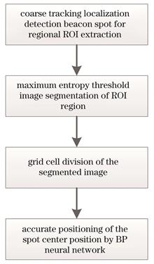
ObjectiveSpace optical communication has been rapidly developed in recent years because of its advantages, which include a high transmission rate, strong anti-interference, good confidentiality, and small equipment sizes. Although space optical communication has many advantages, there are also atmospheric factors, such as atmospheric scattering attenuation, turbulence flicker, and turbulence speckle, that cause various degrees of interference to lasers. Hence, the quality of the light spot received by the receiving end of the communication system will degrade, and the detection accuracy of the light spot will also be affected. Therefore, to enhance the stability of optical communication systems in the presence of atmospheric interference, it is imperative to explore the spot localization algorithm.MethodsA grid-based neural network localization algorithm for spot centers is proposed to improve the stability of optical communication systems under atmospheric interference. First, the region of interest (ROI) is extracted from the light spot detected by coarse tracking, and the image is segmented by the maximum entropy thresholding method. Then, the segmented image is divided into grid cells, and the effective response area of each grid cell is separately calculated. Finally, the sequence of the effective response area of each grid is inputted into a pre-trained BP neural network, and the accurate coordinates of the light spot center position are predicted.Results and DiscussionsTo verify the effectiveness of the algorithm proposed in this study, the centroid algorithm, circle-fitting algorithm, and proposed algorithm were used to perform comparative experiments on image spot positioning errors for two sets of images with different types of light spots. The absolute errors of two different types of light spots are shown in Figs. 7 and 8. The results of the absolute errors show that the absolute errors of the proposed algorithm are the smallest. The maximum error is associated with the circle-fitting algorithm, and this is followed by the centroid algorithm. The experimental results of the root mean square values of the absolute error are shown in Table 1. The average value of the root mean square values of the absolute error in the two sets of images using the proposed algorithm is only 70.11% of that of the centroid algorithm and only 52.27% of that of the circle-fitting algorithm. In the experimental results of the absolute error standard deviation in Table 2, the average value of the absolute error standard deviation in the two sets of images using the proposed algorithm is only 77.80% of that of the centroid algorithm and 65.73% of that of the circle-fitting algorithm. Compared with the traditional centroid algorithm and circle-fitting algorithm, the absolute error of the proposed algorithm is minimal, and the spot location accuracy is better.ConclusionsThis study proposes a method for the accurate location of the center of a light spot in space optical communication systems. The maximum entropy threshold image segmentation method is used to segment the ROI of a beacon light spot detected by coarse positioning, and the image is then divided into 2×2 grids. Next, the effective response area of each grid cell is computed and inputted into a pre-trained BP neural network to get the accurate coordinates of the spot center position. The experimental results show that the absolute error of the proposed algorithm is minimal and that the center position of the light spot can be accurately located. The proposed algorithm can effectively inhibit the influence of atmospheric interference on the positioning accuracy of the center of the spot and provide an effective guarantee for the stability of the space optical communication system. Hence, the proposed algorithm has significant practical application value.
Aug. 31, 2024Vol. 51 Issue 17 1706001 (2024)
Yao Zhang, Bohan Sang, Chen Wang, Jianyu Long, Kaihui Wang, Wen Zhou, Bo Liu, and Jianjun Yu
ObjectiveOwing to the rapid growth of Internet traffic, the demand for large transmission capacities has increased significantly. To address the issues of limited device bandwidths and high hardware-update costs, researchers have adopted expansion methods, including wavelength division multiplexing (WDM) and mode division multiplexing (MDM). Optical signal impairments caused by devices and fiber-optic channels render advanced digital signal-processing technology crucial for achieving high-speed fiber-optic communications. Parallel with the emergence and development of deep learning, machine learning-based equalization has been widely adopted in optical communications. Deep neural networks (DNNs), convolutional neural networks (CNNs), and recurrent neural networks (RNNs) have been applied for the nonlinear compensation of fiber-optic communication systems. In recent years, nonlinear equalizers (NLE) based on RNNs have been investigated extensively. Long short-term memory (LSTM) neural networks, as a type of RNN, can solve the issues of gradient disappearance and explosion during training. In this study, WDM, MDM, polarization multiplexing, and advanced digital-signal processing technology were used to construct a homodyne coherent transmission system based on an LSTM neural network equalizer (LSTM-NNE). We successfully equalized 80 channels of 48 GBaud 64-quadrature amplitude modulation (QAM) signals after transmitting 650 km of few-mode fibers (FMFs) on four modes: LP11a, LP11b, LP21a, and LP21b. The bit error rate (BER) of the MDM-WDM system can satisfy the 25% soft-decision forward-error correction (SD-FEC) threshold of 4×10⁻².MethodsAt the transmitter end, 50 GHz spaced 80-channel signals distributed at 1529.9?1561.4 nm are generated. The channels are separated into two groups, where each group used 40 external cavity lasers with 100 GHz spacing (corresponding to C20?C59 and H20?H59 in the ITU standards), and the optical carriers are coupled by two polarization-maintaining arrayed waveguide gratings (PM-AWGs). The coupled carriers are modulated using two independent IQ modulators. The modulators are driven by a four-channel, 64 GSa/s, arbitrary-waveform generator (AWG) programmed to generate 48 GBaud, 64-QAM signals that are pulse shaped using a 1% root-raised-cosine (RRC) filter. The transmitted symbols are generated using true random integers obtained via atmospheric noise such that overfitting caused by a pseudo-random binary sequence (PRBS) can be avoided. Two polarization multiplexing emulators (PMEs) are used to generate the PDM signals. The optical signal entering the PME is first split into two beams by a 1×2 coupler, decorrelated through optical fibers of different lengths, and then combined by a polarization beam combiner. The two 40-wavelength PDM signals are coupled and amplified using an erbium-doped fiber amplifier (EDFA), after which the coupled signal is split and delayed to generate four tributaries with a relative delay of 100 ns and then fed into four parallel path-length-aligned recirculating loops. Before adding the 100 ns relative delay, we fine-tuned the initial delay fiber length such that the mode sync peaks in frame synchronization appeared at the same location, thereby allowing the total delay spread to be reduced. The single-mode outputs of the four loops are amplified to 23 dBm and multiplexed using a mode multiplexer. The obtained four-mode signals are launched into a 50-km-long span of the FMF. The output of the FMF is demultiplexed, and the signals are amplified using four EDFAs. Four wavelength-selective switches operating within the C band with 50 GHz channel spacing are used to add independent attenuation for each channel to compensate for the uneven gain of the EDFA. At the receiver end, the outputs of the four loops passed through four wavelength-division demultiplexers (DWDMs). The output signals are received by four coherent receivers (CRs) for homodyne reception. We used a real-time digital storage oscilloscope (DSO) to capture the baseband electrical signal and perform offline DSP, which comprised resampling, CD compensation, frequency-offset compensation, frame synchronization, and the proposed LSTM-NNE, which is first initialized in the data-aided mode and then switched to the decision-directed mode for BER calculation.Results and DiscussionsFigure 4 shows the BER of the conventional MIMO-LMS (multi-input multi-output least mean square), NNE, and the LSTM-NNE proposed herein for different transmission distances. The BER yielded by the LSTM-NNE is approximately 0.01 lower than that yielded by the NNE, whereas it is even lower compared with that yielded by the conventional MIMO-LMS algorithm. Meanwhile, the LSTM-NNE enables the BER of the 64-QAM to be transmitted 650 km lower than the 4.0×10⁻² SD-FEC threshold. As shown in Figs. 5 and 6, the difference in BER of each mode under different wavelength subchannels is insignificant. Furthermore, the BER of each channel in the 650 km transmission is lower than the 4.0×10⁻² SD-FEC threshold.ConclusionsIn this study, we constructed a four-mode 80-wavelength dual-polarization homodyne coherent transmission system. At the receiving end, an LSTM neural network equalizer was used for channel equalization. When transmitting 650 km, the net rate of the transmission system reached 147.4 Tbit/s. By utilizing the LSTM-NNE, the BER of the MDM-WDM system can satisfy the 25% SD-FEC threshold of 4×10⁻². The experimental results confirmed the nonlinear equalization potential of the MIMO neural network equalizer for future high-capacity long-distance transmission systems.
Aug. 30, 2024Vol. 51 Issue 17 1706002 (2024)
Xiaoxue Kang, Na Chen, Shaoying Li, Zhenmin Liu, Shupeng Liu, Yana Shang, Wei Huang, Hongliang Lu, and Tingyun Wang
ObjectiveTemperature and electroluminescence spectra are critical for the reliability characterization of gallium nitride (GaN) devices. The traditional method of reliability characterization combines the existing temperature measurement and electroluminescence detection. The temperature measurement method is mainly used to measure the lattice temperature and Joule heating. Electroluminescence is primarily used to measure gate current leakage, thermal electrons, and electric fields, which complement each other. Because the electroluminescence spectrum is correlated with temperature, it is necessary to characterize the temperature simultaneously with the measurement of the electroluminescence spectrum to avoid the influence of lattice temperature on the electroluminescence spectrum. Therefore, the simultaneous characterization of the electroluminescence spectrum and in situ temperature is important for the reliability evaluation of GaN devices. Currently, the measurement of the electroluminescence spectrum mainly uses an electroluminescence spectrometer, and temperature characterization method includes micro-Raman spectroscope, thermoreflectance, and scanning thermal field microscope. However, these methods cannot achieve simultaneous in-situ measurement of the electroluminescence spectrum and temperature in micro-nano regions. The core component of scanning probe microscopy (SPM) technology is the fiber probe, which has the ability to transmit optical signals and collect near-field optical signals. However, the conventional fiber probe cannot be used for temperature measurement, whereas the cadmium selenide quantum dot (QD)-modified fiber probe is verified to be suitable for the nondestructive detection of the temperature of living cells. In this study, we propose a new near-field simultaneous measurement method for the electroluminescence spectrum and in-situ temperature using a cadmium selenide QD-modified fiber probe, which is used to characterize the electroluminescence spectra and near-field temperatures of GaN samples under different voltage excitations.MethodsBased on SPM technology, the QD fiber probe approaches an area of tens of nanometers on the surface of a sample under the control of tuning fork atomic force feedback, and heat is transferred from the sample surface to the QDs at the tip of the probe through the near field. The excitation light is injected through the pigtail of the fiber probe and transmitted through the fiber to the QDs at the tip of the probe, which excites the fluorescence of the QDs. The fluorescence peak of the QDs shifts with increasing temperature. The QD fluorescence signal, which carries temperature information, is collected backward by the fiber probe and then demodulated by the fluorescence spectra as a function of temperature. Simultaneously, the QD fiber probe collects the electroluminescence signal emitted by the surface of the GaN sample through the near field and transmits it to the spectrometer via the probe pigtail to obtain the near-field electroluminescence spectra of GaN. Because the probe tip size is on the order of tens of nanometers, it can achieve high-spatial-resolution near-field simultaneous detection of the electroluminescence spectrum and in-situ temperature. Figure 1(a) shows a schematic of the principle of the electroluminescence spectrum and in-situ temperature simultaneous measurement system based on the QD fiber probe, which is based on an atomic force microscope and Raman spectrometer. The QDs at the tip are excited by a 532 nm laser with an excitation power of 0.2 mW and integration time of 1 s. The calibration relationship between the fluorescence spectrum and temperature is shown in Figs. 1(b) and (c). The temperature sensitivity of the probe is 210 pm/℃, and the temperature measurement error is approximately 0.9 ℃.Results and DiscussionsA GaN sample is prepared on bulk single-crystal GaN material using vacuum evaporation technology; a schematic is shown in Fig. 2(a). To measure the surface height of the GaN sample, a QD fiber probe is used to scan the GaN surface over a large area with a scanning size of 100 m×50 m, as shown in Fig. 2(c). The height of the electrode region is approximately 358 nm, the GaN tends to be relatively flat, and the heights of a few uneven regions reach 705 nm. According to the scanning height, the average roughness of the electrode is approximately 56 nm. The electrode height and roughness are within the control range of the tuning fork spacing, and the probe can be used for the in-situ measurement of this area. To study the electroluminescence characteristics of GaN characterized by the QD fiber probes, the voltage excitation threshold of GaN samples is measured based on the method proposed in this paper, and the measurement results are shown in Fig. 3. When the excitation voltage reaches 9 V, GaN electroluminescence will cause its own impedance to change from 0.23 Ω to 0.10 Ω. Based on this, it is investigated whether the electroluminescence of GaN samples affects the local temperature rise of GaN samples. The measurement results of the GaN power change and surface temperature rise under different voltage excitations and the same voltage excitation time are shown in Fig. 5(a). The temperature gradient in the range of 9?12 V excitation voltage is significantly greater than that in the range of 0?9 V excitation voltage. Based on the analysis in Fig. 3, it can be concluded that this phenomenon is caused by the electroluminescence of the GaN sample. In addition, the temperature rise of GaN and metal electrodes under the condition of 12 V voltage excitation is monitored in real time, and the 1.9 ℃ temperature difference between GaN and metal electrode is measured at 150 s, as shown in Fig. 5(b).ConclusionsIn this study, we propose a method for measuring the electroluminescence spectrum and in-situ temperature of GaN materials in the micro-nano region based on tuning fork feedback QD fiber probes. The GaN samples are detected under different excitation voltages. The results show that the voltage excitation threshold for the electroluminescence of the GaN sample is 9 V, and the peak intensity of the electroluminescence spectra gradually increases with the increase of the excitation voltage. The central peak remains unchanged, and GaN electroluminescence causes its own impedance to change from 0.23 Ω to 0.10 Ω, which affects the change of GaN power. Moreover, the temperature gradient of the GaN surface is significantly greater than that in the excitation voltage range of 9?12 V, which is caused by the GaN electroluminescence. In addition, the temperature rise of GaN and metal electrodes under the power-on and power-off conditions is monitored in real time under the 12 V voltage excitation. The temperature of GaN samples tends to be stable at 150 s, and there is a temperature difference of 1.9 ℃ between GaN and metal electrode. The results show that this method can be used for the near-field simultaneous measurement of GaN micro-nano temperature and electroluminescence spectrum, which has more advantages than the traditional separate measurement methods of electroluminescence and temperature and has promising application prospects in the performance characterization of GaN high-electron-mobility transistors and other semiconductor materials in the future.
Aug. 29, 2024Vol. 51 Issue 17 1706003 (2024)
Weiqin Li, Qing Bai, Wei Zan, Xinyi Liu, Yu Wang, Xin Liu, and Baoquan Jin
ObjectiveTo address the problem of low signal-to-noise ratio (SNR) in long-distance sensing using a single-pulse Brillouin optical time-domain analyzer (BOTDA), a fusion method of pulse coding and denoising convolutional neural network (DnCNN) is proposed to improve the BOTDA SNR over long distances. This method can be widely used in long-distance engineering fields, such as long-distance oil and gas pipeline leakages, optical fiber composite overhead ground wire (OPGW) cable safety warnings, and submarine cable monitoring. When traditional single-pulse BOTDA performs long-distance sensing, it is generally necessary to increase the peak pulse power or the cumulative average number of measurements to obtain higher SNR. However, an excessively high peak input power causes a modulation instability effect, resulting in a decrease in the measurement accuracy of the system. An excessive cumulative average number significantly increases the measurement time of the system. Therefore, a fusion method of pulse code and denoising convolutional neural network (DnCNN) is used to improve the SNR of BOTDA. This method can effectively improve the SNR, extend the sensing distance, and accelerate the measurement speed, while maintaining the spatial resolution of the system.MethodsFirst, the signal strength enhancement principle of Golay coding BOTDA and the noise characteristics of the Brillouin gain spectrum (BGS) are analyzed, and the SNR enhancement scheme of the Golay coding fusion DnCNN is constructed. Under similar experimental conditions, the BGS along the fiber is acquired using single-pulse and Golay coding, and the BGS acquired using Golay coding is denoised using a trained DnCNN. Subsequently, the peak pulse power is increased to 110 mW, and single-pulse measurement signals averaged 2000 times are collected and compared with the signals obtained by the fusion method averaged 100 times. The results are compared at 5 m spatial resolution and root mean square error (RMSE) of the temperature change area of less than 0.2 MHz. The block-matching 3D filtering algorithm (BM3D), complete ensemble empirical mode decomposition with adaptive noise combined with wavelet threshold (CEEMDAN-WT), and DnCNN are used to reduce the noise of the data collected using the Golay coding, and the effects and running times of different noise reduction methods are compared. Finally, a gradient-temperature experiment is conducted to verify the effectiveness of the fusion method at different temperatures.Results and DiscussionsThe results of the experiments show that compared with the single-pulse modulation mode, at the same pulse peak power, the fusion method can increase the system sensing distance from 10.8 km to 100 km, and the SNR at 10.8 km is increased by 18.92 dB. Compared with the Golay coding modulation mode, the fusion method increases the SNR by 9.17 dB at the 100 km end (Fig. 9). It is further verified that at 5 m spatial resolution and RMSE of temperature change area of less than 0.2 MHz, the cumulative average times required by the fusion method decreases from 2000 times to 100 times, and the measurement time is shortened from 1056 s to 194 s compared with single-pulse modulation (Fig.12). Comparing the time required by BM3D, CEEMDAN-WT, and DnCNN to reduce the noise of the experimental data, DnCNN only took 4.62 s, whereas BM3D and CEEMDAN-WT required approximately 8 h and 27 h, respectively (Fig. 13). The Brillouin frequency shift (BFS) and temperature change in the BFS curve obtained by the fusion method maintains a good linear relationship, and the temperature information along the fiber can be accurately restored at different temperatures (Fig. 14).ConclusionsIn this study, a fusion method of pulse coding and denoising convolutional neural network (DnCNN) is proposed. This method can increase the sensing distance of the BOTDA system from 10.8 km to 100 km under a cumulative average of 100 times and a pulse peak power of 18 mW, and the SNR along the fiber is improved. At a measurement accuracy of 100 km sensing distance, 5 m spatial resolution, and RMSE of temperature change area of less than 0.2 MHz, the measurement time of the fusion method is shortened from 1056 s to 194 s compared with the single-pulse method. This fusion method can be used to measure the temperature in long-distance oil and gas pipeline leakages, OPGW cable safety warnings, submarine cable monitoring, and other engineering fields.
Sep. 10, 2024Vol. 51 Issue 17 1706004 (2024)
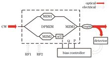
Xinyu Chen, Ren Zhu, Shaowen Lu, Xia Hou, Yaohui Du, Hui He, Xiaozhi Zhu, and Weibiao Chen
ObjectiveWith the continuous development of communication technology, the space laser communication system and standards are also constantly evolving and improving. The modulation technology types for space laser communication are varied. The traditional space laser communication generally adopts the intensity modulation/direct detection (IM/DD) mode, which is easy to implement and economical but has low detection sensitivity and is prone to interference. In contrast, laser communication systems with phase modulation/coherent detection have good wavelength selectivity, allowing for high-speed data transmission while maintaining high reception sensitivity. Most laser communication devices only have a single modulation communication method, which results in a single application scenario and poor interconnectivity among various engineering projects, and can no longer satisfy the requirements of satellite internet. Because different communication systems have different advantages and disadvantages, they are suitable for different application scenarios. If multiple modulation formats can be compatible with a single system and can be switched freely, then this system is suitable for various practical conditions, significantly improving the reliability, flexibility, and efficiency of space optical communication systems. Moreover, communication costs can be reduced by selecting the appropriate communication system. Therefore, many researchers have studied laser communication systems that are compatible and switchable with multiple modulation formats.MethodsThe multi-compatible system developed in this study is based on a double parallel Mach-Zehnder modulator (DPMZM). Multiple emission formats can be achieved by changing the bias voltage on the DPMZM electrodes to operate at different operating points. First, we introduce the bias control method, which combines power and pilot detection methods. It uses a stepwise control method, which is mainly divided into two steps: coarse scanning and fine tracking. In the coarse scanning process, the power detection method is mainly used with a large step value; in the fine tracking process, the pilot signal method is mainly used with a small step value. Second, a numerical simulation of the pilot signal method is conducted to demonstrate the feasibility of the bias control method. Subsequently, a multi-compatible optical emission system is designed using field programmable gate array (FPGA) to interact with multiple modules and achieve multiformat optical emission and coherent demodulation functions. Furthermore, we build a test block diagram for this system and test its transmission signal quality and receiver performance, and conduct thermal vacuum experiments. Finally, we conduct a simulated space environment experiment to verify the adaptability of this system to micro-vibrations in satellite laser communication environments.Results and DiscussionsThe simulation results confirm that the feedback signals of each branch in the pilot method of the bias control algorithm employed in this study exhibit a contrast exceeding 20 dB under ±0.05 Vπ offset (Figs. 5 and 6), thereby satisfying the system’s design requirements. During testing of emission performance in the multicompatible system, the quadrature phase shift keying (QPSK) transmission signal at a 5 Gbit/s rate is repeatedly tested at room temperature, yielding test results that consistently surpass 9%, with the lowest error vector magnitude (EVM) reaching 5.03% [Fig. 11(a)]. The binary phase shift keying (BPSK) transmission signal at a 2.5 Gbit/s rate exhibits the lowest EVM of 3.43% [Fig. 11(b)], whereas the on-off keying (OOK) transmission signal at the same rate has an EVM of 3.76% [Fig. 11(c)]. To assess the overall communication performance of the system, the transmitting system is integrated with the receiving demodulation system. Under an optical power of -50 dBm, the bit error rate (BER) measured by the system is 3.9×10⁻³ (Fig. 12). Additionally, the stability is verified in a thermal vacuum environment test. At an optical power of -47.5 dBm, the BER test results for 9 h of continuous operation exhibit an overall stability of 1×10⁻⁴ (Fig. 13). Furthermore, in the simulated space environment test, the system is loaded with NASDA spectrum, resulting in a BER higher than 8×10⁻⁶ (Fig. 15). These findings demonstrate the terminal’s adaptability to micro-vibrations in satellite laser communication environments.ConclusionsIn this study, we developed a multi-compatible system, which is based on a closed-loop bias control algorithm and is compatible with OOK/BPSK/QPSK. When transmitting QPSK signals with a communication rate of 5 Gbit/s, the receiver’s communication sensitivity reaches -50 dBm, the decoding BER is less than 1×10⁻⁷, and the transmission EVM is lower than 9%. It can provide high-speed and high-quality optical signal sources for space laser communication. Through experimental verification, the communication system has good vacuum and temperature adaptability as well as good adaptability to microvibrations in the space environment. It can effectively address the unification of different constellations and has important research significance.
Sep. 03, 2024Vol. 51 Issue 17 1706005 (2024)
Ningzhe Li, Jinsheng Jia, Min Zhang, Yuze Wang, Feng Xiao, Qing Huang, Shengchuang Bai, Shiryaev Vladimir, Shixun Dai, Qiuhua Nie, and Xunsi Wang
ObjectivePhotonic crystal fiber (PCF) has a variety of unique optical properties, such as single-mode transmission in all wavelength ranges, large effective mode area, high nonlinearity, and dispersion control, which make it have a wide range of applications. The transmission ability of a traditional PCF is restricted by air core collapse and structured cladding deformation during optical fiber fabrication. The all-solid-state structure can solve the problems of air hole collapse and cladding deformation of traditional PCF. The large mode area (LMA) PCF can solve the nonlinear effects such as four-wave mixing and Brillouin scattering caused by the small mode field area of the traditional PCF. Therefore, large mode area single-mode all-solid-state PCF is a good carrier for high-power fiber lasers and amplifiers and the only effective way to improve the power processing capability of chalcogenide fibers while maintaining beam quality. In this study, a large mode area single-mode all-solid-state chalcogenide PCF is prepared by extrusion-stacking method, which solves the problem that traditional fibers could not achieve high power transmission and high beam quality at the same time.MethodsIn this study, we first establish a theoretical model for large mode area single-mode all-solid-state chalcogenide PCF. Mid-infrared chalcogenide glass Ge10As22Se68 and As2S3 are chosen as high and low refractive index materials. The fiber is prepared by extrusion-stacking method. Firstly, the two materials are extruded into rods, and then the rods are stacked according to the theoretical model to obtain preforms. Finally, the preform is drawn into fiber. The cross section, mode area, near-field energy distribution, fiber loss and bending loss of the fiber are calculated and analyzed.Results and DiscussionsAccording to the simulation results, the optimal structural parameters of large mode area single-mode all-solid-state chalcogenide PCFs are obtained. The experimental results show that large mode area single-mode chalcogenide PCF can simultaneously achieve high power transmission and high beam quality. Based on the cross section of the large mode field single-mode all-solid-state chalcogenide PCF [Fig. 8(a)], the mode field area of the fiber is about 5400 μm2. From the spot diagram [Fig. 8(b)] and energy distribution diagram [Fig. 8(c)] measured by the near-infrared fiber field analyzer at 1.55 μm, it can be seen that the optical fiber transmission intensity distribution is Gaussian distribution, which proves that the large mode area all-solid-state chalcogenide PCF realizes single-mode transmission. The fiber losses of the prepared large mode area single-mode all-solid-state chalcogenide PCF and the cladding-free Ge10As22Se68 fiber are tested. The truncation method is used for multiple measurements and the average value is calculated. The fiber end face is kept intact with a precision fiber cutter to obtain the fiber loss diagram (Fig. 9). It can be seen that the PCF loss is much larger than the loss of the cladding-free fiber, that is, the loss of the matrix glass. The reason for this additional loss may be the leakage of light energy caused by the structural defects of the fiber and the defects formed by the stacking interface. Through the bending loss performance test of the large mode area single-mode all-solid-state chalcogenide PCF (Fig. 10), it is found that the loss in the fiber core increases with the decrease of the bending radius, and the change is obvious at 12 cm bending radius. The low bending loss of 1 dB is observed in the fiber with a bending radius of 14 cm, which is consistent with the simulation results of COMSOL. It can be seen that the prepared fiber has good bending resistance.ConclusionsAiming at the current problem that the high-power transmission and high beam quality are difficult to achieve at the same time in chalcogenide fiber, we simulate the properties of the fiber by COMSOL software, and design the structural parameters of PCF that satisfies single-mode transmission and has a large mode field area. The designed fiber satisfies the single-mode condition that the confinement loss ratio of the high-order mode (LP11) to the fundamental mode (LP01) is greater than 102 in the range of 1.5?10 μm, and the effective mode area of the fundamental mode is about 5362 μm2 at 2 μm. According to the structural parameters of the simulation, high-purity chalcogenide glass is prepared by a new combination of dynamic and static distillation. Combined with a novel extrusion-stacking method, an all-solid-state single-mode large-mode-area PCF is prepared based on chalcogenide glass. The optical energy distribution and intensity test results of the fiber at a wavelength of 1.55 μm confirm the single-mode transmission characteristics. At the same time, a low bending loss of 1 dB is observed in a 1.5 m long fiber with a bending radius of 14 cm, which is basically consistent with the simulation results. It is shown that this all-solid-state PCF has excellent single-mode transmission and bending resistance, and has the potential for mid-infrared high-power laser applications.
Aug. 30, 2024Vol. 51 Issue 17 1706006 (2024)
Xiang Tang, Jingtao Xin, Kun Li, Jun Wu, and Mingli Dong
ObjectiveVibration measurement plays essential roles in machinery fault diagnosis and structural health monitoring, and vibration sensors are the most important tools for measuring equipment. Electrical vibration sensor technology is relatively mature and inexpensive. However, there are drawbacks, such as poor circuit stability, poor signal noise, and easy electromagnetic interference. In contrast, fiber Bragg grating vibration sensors have numerous advantages, such as resistances to electromagnetic interference, high and low temperature resistance, and corrosion resistance. Hence, they are widely used in aerospace, large-scale structure monitoring, industrial propulsion, and so on. Miniaturization, multidimensional measurement, and high sensitivity remain as challenges that the sensor must overcome. Therefore, in this study, a three-axis vibration sensor is designed based on a four-core fiber grating. A four-core fiber is employed as an elastic component to detect vibrations in various directions. We anticipate that the issues of sensor miniaturization, multidimensional measurements, and high sensitivity can be resolved with the aid of our structural design.MethodsThe bending sensing principle of a multi-core fiber is analyzed theoretically, and a sensor model is constructed using software. The amplitude-frequency response characteristics of the sensor model are studied using finite element simulations, and the performance of the sensor is analyzed. Finally, a four-core fiber with a diameter of 0.125 mm is identified. The grating area of the four-core fiber is 1 mm long. Brass is used for the sensor mass block, and low-density aluminum serves as the material for the sensor casing. A nickel-titanium alloy tube is also inserted outside the grating region of the four-core fiber to protect it from damage and prevent the fiber from bending when vibration is detected. The sensor is packaged using the sensor packaging platform depicted in Fig. 7 after the sensor parameters are established. This platform ensures that the sensor is packaged with the line and angular positioning accuracies both exceeding 0.1°. The amplitude is shown in Fig. 9, and the amplitude-frequency response characteristics and sensitivity characteristics of the sensor are studied.Results and DiscussionsIn this study, a three-axis vibration sensor is designed based on a four-core fiber grating. A four-core fiber is used as the elastic element of the sensor. This principle is illustrated in Fig. 1. When the sensor detects external vibrations, the mass block inside the sensor is excited and vibrates, resulting in a four-core fiber bend. Inside the four-core fiber, the two cores are located on the plane in the vibration direction, with one being compressed and the other being stretched. The wavelength drifts of the two fiber gratings are the same, and their directions are opposite. Therefore, acceleration in the vibration direction can be calculated based on the real-time wavelength difference between the two gratings. Simultaneously, owing to the characteristics of the four-core fiber itself, a single four-core fiber grating can only achieve vibration monitoring in two directions. Therefore, when designing the sensor structure, the two four-core fibers are interleaved. One of the four-core fibers detects the vibration in the x- and z-directions, and the other four-core fiber detects the vibration in the x- and z-directions so that the sensor can achieve vibration monitoring in three directions. The final packaged sensor is shown in Fig. 8.ConclusionsIn this study, a three-axis vibration sensor based on a four-core fiber grating is designed. The size of the sensor is small: 15 mm×15 mm×15 mm. The performance of the sensor is analyzed via theory and finite element simulations, and a packaging platform and vibration test system are built to complete the packaging and performance testing of the sensor. The amplitude-frequency response and sensitivity characteristics of the sensor are tested using a sensor test system. The experimental results show that the operating frequency band of the sensor is 0?300 Hz, the characteristic frequency in the x, y and z directions is 450 Hz, and the sensitivities in the three directions are 30.5 pm/g, 32.07 pm/g, and 29.38 pm/g, respectively. The sensor designed in this study uses a four-core optical fiber as an elastic element, has a simple structure, and can be miniaturized. Simultaneously, two four-core optical fibers are combined to realize three-axis vibration monitoring in space, which has applications in remote-sensing satellites and other fields.
Sep. 01, 2024Vol. 51 Issue 17 1706007 (2024)
Yanrui Sun, and Yuan Ji
ObjectiveWith the continued popularity of the meta-universe and the advancement of virtual reality (VR) technology, users are more eager to get a perfect immersive experience. People enter the meta-universe mainly through near-eye displays. In contrast, the advantages of silicon-based organic light-emitting diode (OLED) microdisplays such as high resolution, small size and light weight can greatly improve immersion experience. At the same time, digitally driven microdisplays have the advantages of low cost, low power consumption, high refresh rate and high contrast. However, current device bandwidths cannot support the amount of data that increases with resolution and refresh rate. In order to ensure the subjective and objective quality of the image while greatly reducing the amount of data transmission, efficient data compression technology is the key to the application.MethodsIn the digitally driven subfield scanning method of silicon microdisplay, the total display time of an image frame is often divided into several different integer or fractional subfields, and the application of just noticeable difference (JND) model to the data compression of fractional subfields has become the main direction of research. The traditional JND model is mainly inspired by the working mechanism of the human vision system, and uses the relevant characteristics of human vision to extract image features through design formulas, so as to construct the model. At present, the distortion introduced by JND model established by subjective experiment is usually additive noise such as white noise. The flat region with low image gradient is more affected by it, and the distortion is more perceptible. The distortion in the edge region with large gradient is difficult to detect. However, multiplicative noise occupies a larger proportion in actual coding, and the block effect has a greater influence on the edge region than the flat region. Therefore, we further consider the masking effect of stereovision, and design masking characteristics experiments of foveal and block effects. Meanwhile, this paper presents a cruciate block (CB) compression algorithm based on variable number of bit-planes, which adopts different number of bit-plane compression for different number of subfields. The gray level of the original image is modified by the CB-FJND model, that is, the pixel gray value is adjusted upward or downward, and the difference should meet the minimum perceptible threshold determined by the CB-FJND model. In order to improve the subjective and objective quality of the image after data compression, a cruciate block compression algorithm based on row and column alternating encoding is proposed in this paper. The row and column encoding of the binary image is adopted successively, and the subfield weights are divided according to certain strategies.Results and DiscussionsIt can be seen from the 16th bit-plane distribution of the image corrected by the CB-FJND model and the change of run length according to the row run length encoding (Fig. 7 and Table 3) that, the numbers of consecutive zeros and ones increase significantly after model intervention, which could significantly improve the compression effect of subsequent run encoding. The higher 15 bit-planes in the bit-plane image present the outline of the original image, while the lower bit-planes corresponding to the fractional subfield present the details of the original image. The lower the bit plane, the more the noise and the less the details. The larger the first plane weight of the fractional subfield is, the higher the image quality is. The more dispersive the weight distribution is, the lower the image quality is. Therefore, the fractional subfield weights can be divided according to the optimal weight distribution strategy under the multi-subfield configuration, which can ensure the compression rate and improve the objective quality of the image (Tables 5 and 6). In the aspect of image coding, the CB compression algorithm using cruciate encoding method can greatly improve the subjective quality of image while ensuring the compression rate of image, and eliminate the phenomenon of horizontal and vertical stripes which may exist in the image compressed with other algorithms (Fig. 8, Fig. 11, and Table 7). Therefore, the cruciate block compression algorithm based on CB-FJND can provide better compression effect.ConclusionsIn this paper, based on the existing JND model of stereoscopic image, the influence factors of block effect are added, and the CB-FJND model is established to calculate the visual redundancy of the image more accurately. In order to meet the need of dynamic false contour (DFC) and gamma correction, multiple subfield bit-planes are introduced to compress the input data, and the optimal weight distribution strategy of the fractional subfield is proposed. According to the existing compression methods, a cruciate block compression algorithm is proposed. The hardware feasibility of the algorithm is verified on field programmable gate array (FPGA) platform. The experimental results show that the multiple bit-plane cruciate block compression algorithm based on CB-FJND model can greatly reduce the stereoscopic image transmission data in virtual reality to less than 40% and solve the distortion caused by excessive image data compression, ensuring the image quality, and providing a solution for increasing the user's visual experience and equipment bandwidth limitation in virtual reality.
Aug. 29, 2024Vol. 51 Issue 17 1709001 (2024)
Zuqiang Li, Qi Xiao, Xue Pan, Xinghua Lu, Jiangfeng Wang, Shengjia Zhang, Xiaochao Wang, Youen Jiang, Wei Fan, Xuechun Li, and Jianqiang Zhu
ObjectiveIn recent years, thin-disk lasers have been applied in various fields such as basic scientific research, industrial production, biomedicine, and defense. Owing to their significant advantages in terms of power scalability, thermal performance, and nonlinear effects, thin-disk lasers show promise for combining high average power and high peak power with excellent beam quality. Regenerative amplification is the technology that best suits thin disk lasers. The output power of the amplifier is increased by increasing gains and reducing the losses. Currently, regenerative amplifiers typically increase the gain by either enlarging the pump area or employing multiple thin-disk modules. However, in the former method, the amplified spontaneous emission (ASE) also increases simultaneously, whereas the latter method involves a more complex and uneconomical optical path. Double-pass regeneration is a promising technology in which a beam passes through a thin disk four times in a round trip, ultimately reducing the total loss by decreasing the number of round trips. In this study, we report a compact Yb∶YAG thin-disk double-pass regenerative amplifier. The amplifier has a maximum output power of 130 W and an optical-to-optical efficiency of 26%.MethodsThe thermal focal length of a thin-disk medium determines the mode distribution in the resonator cavity and should be measured before designing the cavity. Using a wavefront sensor based on the principle of four-wave lateral shearing interferometry, the thermal focal length is measured at various pump power levels. By applying the ABCD matrix theory, the optical resonator of the thin-disk regenerative amplifier is designed and optimized to ensure operation in the fundamental mode and insensitivity to cavity misalignment. The pulses are passed through the thin-disk medium twice at intervals longer than the pulse width. Additionally, the beam diameters in the medium are similar. The optical layout of the thin-disk double-pass regenerative amplifier is shown in Fig. 1. It includes a seed laser with a narrow spectral width, optical isolator, Faraday rotator, Pockels cell, thin-film polarizers, resonator cavity, and Yb∶YAG thin-disk module with a 24-pass pumping system. The thin-disk module consists of a doped Yb∶YAG thin-disk crystal with a 9 mm aperture and a thickness of 215 μm. The pump laser can deliver power up to 500 W at a wavelength of 969 nm. The multipass pump spot on the Yb∶YAG thin-disk crystal has a circular shape with a super-Gaussian distribution, and its diameter is approximately 3.9 mm. In addition, the particle rate equation is used to calculate the saturated output pulse energy values of the single-pass and double-pass regenerative amplifiers at a continuous pump power of 500 W. The results indicate a significant improvement in the output of the optimized cavity.Results and DiscussionsWhen a single longitudinal-mode seed laser with a pulse width of 3.4 ns, repetition rate of 10 kHz, and energy of approximately 1 nJ is injected for amplification, the regenerative amplifier delivers an average power of 130 W at a pump power of 500 W. This results in an optical-to-optical efficiency of 26%. The amplifier outputs a pulse close to the diffraction limit with beam quality factors of 1.20 and 1.15 in the horizontal and vertical directions, respectively. The near- and far-field patterns of the amplified beam are measured, and are shown in the insets of Figs. 5 and 8, respectively. Another advantage of double-pass regenerative amplification is the reduced impact of the cavity offset on stability. This is owing to the reduction in the number of round trips. The peak-to-valley values (PVs) and root mean square (RMS) of output power stability for the double-pass regenerative amplifier within 3.5 h are 5.77% and 0.77%, respectively. When amplifying the pulses with a repetition rate of 1 kHz, the amplifier delivers an average power of 67 W at a pump power of 500 W. The corresponding optical-to-optical efficiency is 13.3%. In addition, we measure the output powers of the pulses with multiple repetition rates at a pump power of 500 W, as shown in Fig. 9. The waveforms of the pulses with repetition rates of 1 kHz and 10 kHz at the maximum output power are measured, with some waveform distortion occurring in the former.ConclusionsIn this study, we present the results of our study on a double-pass regenerative amplifier that utilizes a single Yb∶YAG thin-disk module. When the pump power is 500 W, the amplifier delivers output powers of 67 W and 130 W at repetition rates of 1 kHz and 10 kHz, respectively. The corresponding optical-to-optical efficiencies are 13.4% and 26%. The output beam is close to the diffraction limit. The cavity type of the double-pass regenerative amplifier shows good stability, with PVs and RMS of output power stability measuring 5.77% and 0.77%, respectively, within 3.5 h. Thin-disk double-pass regenerative amplifiers demonstrate excellent performance. In the future, we will continue to increase the pump power or the mode diameter to achieve improved laser output. In addition, we will amplify the broadened nanosecond chirp pulse to obtain a high-repetition picosecond laser output.
Aug. 29, 2024Vol. 51 Issue 17 1701001 (2024)
Kuikui Li, Weiqiao Zhang, Fengxin Dong, Jianxin Zhang, and Xuyan Zhou
ObjectiveThe quest for high efficiency, compactness, and lightweight design in fiber-coupled laser diode modules is becoming increasingly prominent, particularly within the solid-state laser domain and other fields where high integration or portability is demanded. Given the considerations of cost and the complexities involved in mounting and tuning, laser diode stacks emerge as the preferred sources for high-power fiber-coupled laser diodes. Nonetheless, the pronounced disparity in beam quality across the fast and slow axes presents challenges in accomplishing efficient coupling. To bridge this quality gap, it is imperative to tailor the beam profile of the laser diode stack accordingly. Currently, geometric beam shaping is considered as the prevalent technique for modifying the output of laser diode stacks, enabling beam manipulation without altering the inherent output traits of the laser. This method primarily involves the cutting and reconfiguration of beams through the use of parallel plates or similar optical elements. However, this conventional approach leans on an extensive array of prisms, leading to cumbersome systems. A significant drawback is that optical components are limited to singular functions, lacking in integration. Thus, devising a cohesive beam-shaping strategy is vital for the advancement of integrated fiber-coupled laser diode systems.MethodsTo address the issues concerning the poor beam quality of the laser diode stack and the complexity of beam shaping elements, we propose a new cut-compression-rotation-rearrangement beam shaping method for the laser diode stack and design a stepped rotation rearrangement prism. First, to realize an efficient collimation effect, we collimate the beam by using fast and slow axis collimation lenses with effective focal lengths of 0.3 mm and 8 mm, respectively, resulting in a parallel beam. Subsequently, the designed stepped rotation rearrangement prism is utilized for cutting the beam in the direction of the slow axis in a staggered arrangement. The rotational rearrangement of the beam is realized through two total reflections of light to achieve a dense arrangement of light spots. Then, to effectively reduce the focused spot and obtain a higher energy density, by using beam expansion, a spot with a slow-axis beam width of 9 mm and a residual divergence angle of 4.65 mrad is produced. Finally, an aspherical lens with a focal length of 25 mm is selected for the purpose of focusing, facilitating the coupling of the spot into the target fiber.Results and DiscussionsThe beam parameter products in the fast and slow axis directions after collimation are 12.62 mm·mrad and 17.46 mm·mrad, respectively (Fig. 1). However, the filling factor in the fast-axis direction is low, and there is a large dark area. Subsequently, the collimated beam passes through the stepped rotation rearrangement prism to eliminate the dark area (Fig. 3). The entire beam shaping process of cutting, compression, rotation, and rearrangement of the beam is accomplished by utilizing two total reflections of the beam, without the need for a prism stack. The consideration of aberration and material effects on the beam-shaping process is deemed unnecessary. At this time, the beam parameter products in the fast and slow axis directions are 5.39 mm·mrad and 10.48 mm·mrad, respectively, which satisfy the conditions for fiber coupling. To effectively reduce the focused spot and obtain a higher energy density, the shaped spot must be expanded. A 3× Galilean beam expansion system is constructed using a flat concave cylindrical lens having an effective focal length of -6.35 mm and a flat convex cylindrical lens having an effective focal length of 19 mm. Following this beam expansion system, the slow-axis beam width increases to 9 mm, which is equivalent to a 4.65 mrad residual divergence angle (Fig. 4). After the beam is expanded and focused, it can be coupled into a fiber with a numerical aperture of 0.22 and a core diameter of 200 µm (Fig. 5).ConclusionsIn summary, we propose a new cut-compression-rotation-rearrangement beam shaping method for the laser diode stack. The stepped rotation rearrangement prism beam shaping device, created using this method, only requires the use of multiple identical stepped compression rotation rearrangement prisms to realize the entire beam shaping process, in contrast to traditional beam shaping devices. This significantly simplifies the beam shaping process and minimizes the overall system size. According to the simulation results, a laser diode stack consisting of eight bars can be coupled into a fiber with a core diameter of 200 µm and numerical aperture of 0.22 by using a stepped rotation rearrangement prism. The resulting fiber has an output power of 455.4 W and a fiber coupling efficiency of 94.9%. The system measures a mere 20 mm×60 mm×15 mm, making it compact and highly suitable for solid-state laser pumping.
Sep. 10, 2024Vol. 51 Issue 17 1701002 (2024)
Jinpeng Zou, Cong Yin, Jianbo Wang, Wenwen Bi, Mingyu Zhang, and Yixuan Zhu
To assess the long-term stability of the laser wavelength, a 14-h beat frequency experiment is conducted using an optical frequency comb as the reference laser. The experimental results are presented in Fig. 11. The findings indicate that over the 14-h measurement period, the average vacuum frequency value obtained is 473612353616 kHz, with a deviation of 12 kHz from the internationally recommended value by the International Committee for Weights and Measures. Without altering the analog PID parameters, the laser overall PID gain is adjusted through a digital potentiometer. The wavelength stability (Allan standard deviation) of the laser, as determined by the beat frequency with an optical frequency comb, before and after PID gain adjustment, is illustrated in Fig. 12. Maintaining the same PID parameters and appropriately adjusting the overall PID gain after locking contribute to an improvement in frequency stability. After gain adjustment, the frequency stability is measured as 7.3×10⁻¹¹ for 0.1 s, 1.4×10⁻¹¹ for 1 s, 3.0×10⁻¹² for 10 s, 8.5×10⁻¹³ for 100 s, 3.1×10⁻¹³ for 103 s, and 2.0×10⁻¹³ for 104 s. The experimental results demonstrate that the laser exhibits a high level of frequency stability.ObjectiveBased on the principle of iodine molecule saturation absorption for frequency stabilization, the 633-nm He-Ne laser holds considerable application value in geometric metrology, precision interferometric measurements, atomic spectroscopy, and gravity measurements. Recently, digital metrology has emerged as the future direction of metrology. Although 633-nm iodine-stabilized He-Ne lasers based on analog control systems offer high frequency stability and cost-effectiveness, their further development is constrained by limitations in intelligence and digitization levels. The 633-nm iodine-stabilized He-Ne laser, which is based on a digital control system, not only satisfies the demands of digitization but is also more suitable for miniaturization. However, due to the precision limitations of the employed analog-digital (AD) and digital-analog (DA) converters, the frequency stabilization performance of the 633-nm iodine-stabilized He-Ne laser based on digital circuits is often less ideal, with frequency stability typically lower than that of iodine-stabilized He-Ne lasers based on purely analog control systems. To address the aforementioned issues, in this study, a 633-nm iodine-stabilized laser is proposed based on a modulo-mixed control approach. It combines the advantages of high levels of digitization and stability.MethodsThe structure of the laser system is depicted in Fig. 1. The laser comprises two main components: the laser head and control system. The laser head incorporates a self-developed high-power iodine-stabilized He-Ne laser head, comprising a laser tube, iodine cell, high-reflectivity mirror, piezoelectric ceramic, photodetector, and thermoelectric cooling element. The control system consists of two parts: analog circuitry and digital circuitry. The analog circuitry section consists of three parts: a sinusoidal signal generator, an optical power signal demodulator, and a proportional-integral-differential (PID) controller. The sinusoidal signal generator employs a Wien bridge sinusoidal signal generation circuit. By selecting low-temperature drift precision components and finely tuning the component parameters, high-quality output can be realized. The optical power signal demodulator is realized via a mixer. The demodulated third harmonic signal used for locking realizes a satisfactory level, with a signal-to-noise ratio of 8∶1. The PID controller allows for gain adjustment through a digital potentiometer, which is managed by an mirco-controller unit (MCU), expanding the adaptability of laser frequency locking to different scenarios. The digital circuitry section, employing two absorption peak recognition algorithms, achieves automatic locking of absorption peaks. It enables the uploading of laser operational data to a computer, enhancing the digitization level of the laser system. Combining the aforementioned sections, the final design of the laser system is successfully implemented.Results and DiscussionsTo assess the automatic peak-locking functionality of the laser, the newly developed laser is compared with the iodine-stabilized He-Ne laser, a national length standard, with both locked onto the d-peak and g-peak. The frequency difference between the two peaks is set at 39.422 MHz. In the experiment, the newly developed laser is intentionally unlocked, and the locking process is monitored via beat frequency. The experimental results are depicted in Fig. 10. The results demonstrate that the system can successfully relock, with a relocking duration of 30 s. After locking, the laser remains positioned in a stable manner at the target absorption peak.ConclusionsThe 633-nm iodine-stabilized He-Ne laser proposed in this study, based on the modulo-mixed control method, exhibits crucial digital features such as automatic peak recognition. It satisfies the urgent demand in the metrology industry for digitally-enabled length measurement standards. Simultaneously, leveraging analog circuitry technology, the laser achieves high-precision locking of absorption peaks. Experimental results demonstrate a frequency stability of 1.4×10⁻¹¹ for 1 s and 3.1×10⁻¹³ for 103 s, satisfying the metrology industry requirements for high stability in 633-nm iodine-stabilized He-Ne lasers. The laser system presented in this study provides essential technical support for the application of the 633-nm iodine-stabilized He-Ne laser in precision measurements and digital metrology.
Aug. 29, 2024Vol. 51 Issue 17 1701003 (2024)
Benyong Chen, Yong Zhao, Yingtian Lou, Liping Yan, Jiandong Xie, Liang Yu, and Jianjun Tang
ObjectiveTo address the challenges of automatically identifying absorption peaks and the low sensitivity of error signals in the saturated absorption spectrum laser frequency stabilization technique, a method using convolutional neural network (CNN) is proposed for recognizing rubidium atomic absorption peaks. This approach is highly applicable in the realm of saturated absorption spectroscopy laser frequency stabilization. Traditional techniques are limited to identifying and locking onto specific absorption peaks within a narrow laser tuning range, necessitating manual pre-adjustment of the laser frequency close to the absorption peak. However, in practice, the initial laser operating point is often unknown, requiring broad frequency scans to locate the target absorption peak signal. This can result in detecting multiple groups of absorption peaks. Moreover, the process of deriving error signals is complicated with respect to the phase delay between the saturated absorption signal and local oscillator signal, impacting error signal sensitivity. Typically, phase adjustment of the local oscillator signal is manually performed and monitored with an oscilloscope to capture the most sensitive error signal. This method is inefficient and inaccurate, and thereby, fails to satisfy the demands of high-precision automatic laser frequency stabilization. Consequently, a CNN-based laser frequency stabilization method, which intelligently recognizes rubidium atomic absorption peaks and automatically adjusts for phase delay, is introduced to realize long-term precision stabilization of laser frequency.MethodsInitially, a one-dimensional convolutional neural network (CNN) was designed, incorporating a combination of five large and small convolution kernels. This design included “convolution-ReLU-maxpooling” modules followed by two fully connected layers. A linear sweep of the laser frequency was then performed to acquire a spectrum signal from rubidium atoms, containing 24 saturated absorption peaks. The sequence number of each absorption peak was extracted, and these numbers, along with the rubidium atomic spectral signals, were used as labels and data for CNN training, respectively. The trained CNN was then employed for the intelligent identification of absorption peaks. The quadrature demodulation technique was adopted to accurately extract the phase of the saturated absorption spectrum signal and match it with the phase of the local demodulation signal, thereby improving the sensitivity of the error signal. A laser frequency stabilization system, based on CNN intelligent peak search and integrating computer and real-time signal processing with a field-programmable gate array (FPGA), was developed. Locking tests and frequency stability experiments were conducted on this system. It was demonstrated through experimental results that the method of laser frequency stabilization, based on CNN intelligent recognition of rubidium atomic absorption peaks and automatic phase delay matching, can achieve long-term precision stabilization of laser frequency.Results and DiscussionsIn response to the challenges of automatically identifying multiple absorption peaks and the decreased sensitivity of error signals due to phase delay, a laser frequency stabilization method that utilizes convolutional neural network (CNN) to identify rubidium atomic absorption peaks is proposed. The designed one-dimensional CNN model (Fig.4) converges (Fig.5), enabling intelligent recognition of multiple absorption peaks within saturated absorption spectral signals (Fig.6 and Fig.7). Through automatic phase delay matching, the phase delay significantly reduces from 100.93° to 0.02°, leading to increases in both the zero-crossing slope and amplitude of the error signal. This in turn substantially enhances its sensitivity. A laser frequency stabilization system, incorporating CNN-based intelligent peak search with computer and real-time signal processing via FPGA, is developed (Fig.1). This system locks onto the cross peak 85Rb F=3→F′=CO3-4 for a locking test (Fig.11). The locked laser undergoes beat frequency experiments with an optical frequency comb to assess frequency stability. Experimental outcomes reveal that the minimum relative Allan variance over a span of 7500 s is 3.50×10⁻¹² @τ=64 s (Fig.14). This illustrates that the proposed CNN-based approach for intelligent identification of rubidium atomic absorption peaks, coupled with automatic phase delay matching for laser frequency locking, facilitates long-term precise stabilization of laser frequency.ConclusionsIn this study, a laser frequency stabilization technique utilizing CNN is introduced for the intelligent recognition of rubidium atomic absorption peaks. This approach not only facilitates the intelligent identification of multiple absorption peaks across a broad tuning range of lasers but also supports long-term precise laser frequency stabilization. Experimental evidence shows that a specially designed one-dimensional CNN model is capable of accurately identifying 24 absorption peaks within the rubidium atomic spectrum signal. Automatic phase delay adjustment from 100.93° to 0.02° significantly enhances the error signal’s sensitivity. Following the application of laser frequency stabilization, the minimum relative Allan variance decreases to 3.50×10⁻¹², when average time is 64 s. Consequently, this method holds potential for broad application in areas such as saturated absorption spectroscopy and laser frequency stabilization.
Aug. 31, 2024Vol. 51 Issue 17 1701005 (2024)
Zhonghai Yang, Zhen Zhang, Zhigang Zhao, Liangbi Su, and Zhaojun Liu
ObjectiveIn the mid-infrared region, erbium-doped lasers at 2.8 μm have attracted significant attention owing to their wide applications in the medical treatment, detection, and military fields. The phonon energy of erbium-doped crystalline oxides (e.g., Er∶YAG and Er∶YSGG) is high (860 cm-1 and 728 cm-1), which causes the self-termination phenomenon. The phonon energy of erbium-doped sesquioxides, such as Er∶Lu2O3 and Er∶Y2O3, is low (618 cm-1 and 597 cm-1) and the thermal conductivity of these materials is high. However, the fabrication of these active laser materials is complicated and expensive mainly due to their high melting temperature. Erbium-doped fluorides, such as Er∶YLF, Er∶CaF2, and Er∶SrF2, show lower phonon energy (560 cm-1, 322 cm-1, and 280 cm-1) than sesquioxides, which can effectively suppress the non-radiative transition. Especially, the doped Er3+ ions prefer to form clusters in CaF2 and SrF2 crystals. These spontaneous clusters can achieve strong energy transfer between Er3+ ions with very low doping concentration (approximately 1%), accordingly obtaining a high-efficiency and high-power continuous-wave (CW) laser at 2.8 μm. The emission spectrum of Er∶CaF2 and Er∶SrF2 crystals is wide, approximately 250 nm (from 2600 nm to 2850 nm), around 2.8 μm. Therefore, spectral tuning of the Er∶CaF2 laser output wavelength is viable.MethodsTo obtain high-power CW laser, a dual-end pumped Er∶CaF2 laser is demonstrated [Fig. 1(a)]. The two pumping sources are wavelength-stabilized 976 nm fiber coupled laser diodes (LD) with a fiber core diameter of 105 μm and a numerical aperture of 0.22. The pumping radiations are focused into the laser crystal by the optical coupling systems with a coupling ratio of 30∶60 (L1∶L2) and 30∶75 (L4∶L3), respectively. A plane-concave resonator with a cavity length of 23 mm is formed by a concave dichroic mirror (DM1) and a plane output coupler (OC). The DM1, with a radius of curvature of 50 mm, is AR coated (T=95%) for 960?980 nm and HR coated (R=99.8%) for 2.65?2.85 μm. An OC with T=3% at 2.65?2.85 μm is used. The DM2 is placed between the OC and the L3 lens to separate the laser from the pumping radiations. With a dimension of 2 mm×2 mm×20 mm, an uncoated 2%-doped Er∶CaF2 crystal is wrapped with indium foil and placed in a water-cool copper block with a temperature of 18 ℃ for heat dissipation. In addition, a tunable Er∶CaF2 laser is also demonstrated [Fig. 1(b)]. Uncoated MgF2 birefringent filters (BRF), with a diameter of 15 mm and three different thicknesses, 1, 2, and 4 mm, are mounted on a rotating frame and inserted between the Er∶CaF2 crystal and OC at a Brewster angle (θB=53.7°), respectively. The cavity length is approximately 67 mm. The spectral tuning is achieved by rotating the angle between the BRFs optical axis and the incident light.Results and DiscussionsIn the single-end pump scheme, the laser exhibits a saturation trend when the pump power reaches 19.7 W, and a CW output power of 3.54 W with a slope efficiency of 19.6% is obtained (Fig.2). In the dual-end pump scheme, there is still no saturation trend when the pump power reaches 32.5 W. However, to protect the crystal, the pump power is not further increased. The maximum achieved CW output power is 5.04 W with a slope efficiency of 16.5%, a central wavelength of 2799.27 nm, and a beam quality factor of Mx2=5.16 and My2=5.69 [Figs. 2(a) and (b)]. To the best of our knowledge, this is the highest CW output power among all reported LD-end-pumped erbium-doped fluoride crystal lasers at 2.8 μm. The dual-end pump scheme alleviates the saturation trend of the laser, which is an effective scheme to realize high-power CW laser. There is a slight red-shift of the central wavelength with increasing output power (Fig. 3): from 2749.85 nm at a CW output power of 0.5 W to 2799.27 nm at a CW output power of 5.0 W. In addition, the emission spectrum of the 2%-doped Er∶CaF2 crystal is wide, covering a range of approximately 250 nm, from 2600 nm to 2850 nm (Fig. 3). These observations lead us to believe that spectral tuning of the laser output wavelength is feasible. Based on MgF2 BRFs with thicknesses of 1, 2, and 4 mm, Er∶CaF2 lasers with tuning ranges of 168.89 nm (from 2682.55 nm to 2851.44 nm), 148.87 nm (from 2696.96 nm to 2845.83 nm), and 141.17 nm (from 2703.60 nm to 2844.77 nm) are achieved, respectively (Fig. 5). Owing to the strong absorption of the 2.8 μm laser by water molecules and other substances in the air, the tuning power curves are not smooth and the emission spectrum is modulated. A wider spectral tuning range can be obtained by using BRFs with a smaller thickness, but the processing difficulty and price cost will also be greatly increased.ConclusionsIn this work, high-power CW and tunable Er∶CaF2 lasers are demonstrated. In the single-end pump scheme, the output power reaches 3.54 W when pump power is 19.7 W. In the dual-end pump scheme, the CW output power reaches 5.04 W with a slope efficiency of 16.5% and a central wavelength of 2799.27 nm when pump power is 32.5 W. To the best of our knowledge, this is the highest CW output power among all reported LD-end-pumped erbium-doped fluoride crystal lasers at 2.8 μm. Er∶CaF2 lasers with tuning ranges of 168.89 nm, 148.87 nm, and 141.17 nm are achieved by using MgF2 birefringent filters with thicknesses of 1 mm, 2 mm, and 4 mm, respectively. To the best of our knowledge, this is the widest spectral tuning range among all reported erbium-doped fluoride crystal lasers.
Aug. 31, 2024Vol. 51 Issue 17 1701006 (2024)
Ji Shen, Fei Feng, Jie Ma, Peng Liu, Jun Wang, Zhipeng Qin, Guoqiang Xie, Deyuan Shen, and Dingyuan Tang
ObjectiveContinuous and wide-tunable laser sources in the mid-infrared range of 3?5 μm have attracted significant attention in fields such as spectral analysis, remote sensing, medical treatment, environmental monitoring, and optoelectronic countermeasures. Currently, the primary approach to achieve broadly tunable lasers in this wavelength range is nonlinear frequency conversion methods such as those using optical parametric oscillators (OPOs) and optical parametric amplifiers (OPAs). These methods have advantages, such as a wide tuning range and technological maturity. However, they typically require high-performance near-infrared pulsed lasers or narrow-linewidth lasers as pump sources, leading to challenges such as an extensive system volume, relatively complex resonators, low optical conversion efficiency, and high costs. In recent years, increasing attention has been paid to schemes that directly generate tunable mid-infrared lasers, including semiconductor quantum cascade lasers and mid-infrared oscillators based on mid-infrared laser gain media. Among them, the Fe∶ZnSe crystal exhibits broad absorption and emission spectra, large absorption and emission cross-sections, as well as low phonon energy, making it one of the best candidate materials for directly generating broadly tunable mid-infrared laser sources in the 3?5 μm spectral range. Since the first Fe∶ZnSe mid-infrared laser was reported by Adams et al. in 1999, many studies have been conducted on Fe∶ZnSe lasers. However, stable continuous-wave (CW) and wavelength-tunable Fe∶ZnSe lasers have seldom been domestically reported beyond 4 μm in the mid-infrared wavelength. In this study, pumped by a homemade Er∶Y2O3 ceramic laser, CW and wideband tunable Fe∶ZnSe lasers are demonstrated in the 3?5 μm spectral range.MethodsAccording to the Füchtbauer?Ladenburg (F?L) equation, the emission cross-section of a Fe∶ZnSe crystal is influenced by its fluorescence spectrum and spontaneous emission lifetime. Moreover, it has been demonstrated that there is a noticeable redshift in the central wavelength of the fluorescence spectrum of the Fe∶ZnSe crystals with increasing temperature. Therefore, the emission cross section of the Fe∶ZnSe crystals is temperature-dependent. By controlling the operating temperature of the Fe∶ZnSe crystals, it is possible to achieve a temperature-induced gain spectrum shift, enabling a wavelength-tunable output of the Fe∶ZnSe laser. In the experiment, the Er∶Y2O3 ceramic gain medium has a length of 10 mm and a diameter of 1 mm. The atomic fraction of doped Er3+ of the sample is 7%. The two end faces of the ceramic are laser-grade-polished and plated with antireflection films in the 3 μm wavelength band. A compact two-mirror plano?plano resonator is employed for the laser oscillation. The pumping source is a fiber-coupled semiconductor laser with a maximum output power of 100 W centered at 976 nm. The gain medium is mounted on a heat sink and directly water-cooled to remove the heat accumulated during pumping. The temperature of cooling water is maintained at 15 ℃. An output power of 3.77 W with a central wavelength of 2740 nm is obtained using an Er∶Y2O3 ceramic laser. Then, the 2740 nm laser is collimated by a convex lens F3. After being reflected by the two flat mirrors, M2 and M3, it is further focused on the Fe∶ZnSe laser resonator as the pump light through a lens F4. The Fe∶ZnSe crystal used in the experiment is 6.5 mm long and has a cross-section of 3 mm×3 mm, with an Fe2+ concentration of approximately 5×1018 cm-3. The Fe∶ZnSe laser resonator consists of a plano-concave input mirror (M4) with a curvature radius of 100 mm and a plano-plano output mirror (OC2). The output mirror has a transmissivity of approximately 5% in the 4?5 μm wavelength range. The total length of the laser resonator is approximately 68 mm. Based on the ABCD matrix, the laser beam waist radius at the Fe∶ZnSe crystal position is calculated to be ~258 μm. To achieve an effective CW laser operation, it is necessary to cool the Fe∶ZnSe crystal to ensure a sufficiently long upper-level lifetime. In this study, a low-temperature vacuum chamber cooled with liquid nitrogen is designed. The Fe∶ZnSe crystals are wrapped in an indium foil and mounted on a copper heat sink. The copper heat sink is installed on a Dewar inside the vacuum chamber. The vacuum chamber is equipped with CaF2 window plates on both sides. These window plates are coated with broadband antireflection coatings in the mid-infrared range, ensuring a transmissivity of over 96% for both pump and laser wavelengths.Results and DiscussionsFirst, the CW laser characteristics of the Fe∶ZnSe crystal are studied under liquid-nitrogen cooling at 103 K. In the experiment, the maximum output power of the Er∶Y2O3 ceramic laser is set to 3.0 W to ensure stable operation of the pumping source. The corresponding pump power incident on the Fe∶ZnSe crystal is approximately 2.17 W owing to the Fresnel reflection losses and absorption of the optical components. The output power of the Fe∶ZnSe laser is measured using a thermal sensor power meter. The laser threshold for the incident pump power is approximately 231 mW. The laser output power exhibites an approximately linear increase with the incident pump power. When the pump power reaches 2.17 W, a CW laser output of 352 mW is obtained, and the slope efficiency of the incident pump power is approximately 19.2%. The laser spectra are measured using a mid-infrared spectrometer. It exhibits a single-peak structure with a central wavelength of 4.17 μm and a spectral bandwidth of approximately 35 nm. Subsequently, the wavelength tuning performance modulated by the temperature of the Fe∶ZnSe laser is investigated. As the temperature of the Fe∶ZnSe crystal increases, the central wavelength of the laser shifts from 4170 nm at 103 K to 4553 nm at 173 K, resulting in a tuning range of 383 nm. In the experiment, the laser successfully achieves a wide spectral tuning range. When the temperature of the Fe∶ZnSe crystal exceeds 173 K, the upper-level lifetime of the Fe∶ZnSe crystal quickly decreases. Therefore, longer wavelengths are not used in this experiment.ConclusionsBy employing a homemade Er∶Y2O3 ceramic laser as a pump source, stable CW and wideband tunable Fe∶ZnSe lasers are demonstrated. An average output power of 352 mW is obtained at 4170 nm under liquid-nitrogen cooling to 103 K. Furthermore, the wavelength-tuning performance of the Fe∶ZnSe laser modulated by temperature is investigated, and a continuous tuning bandwidth of 383 nm (4170?4553 nm) is successfully achieved in the experiment.
Aug. 29, 2024Vol. 51 Issue 17 1701007 (2024)
Xinyu Liu, YanLin Zhang, Xuechen Cao, Jie Yang, Jing Su, and Huadong Lu
ObjectiveHigh-power, high-beam-quality, all-solid-state 355 nm ultraviolet lasers, with their short wavelengths, easy focusability, and high energy characteristics, are being widely applied in precision machining, biomedical, optical manufacturing, and optical sensing fields. The most common technique by which to achieve 355 nm ultraviolet output is the use of a master oscillator power amplifier (MOPA) to amplify 1064 nm seed light through single or multiple stages. This is followed by triple-frequency conversion outside the cavity. However, the overall complexity of the system is not conducive to the design of high-stability ultraviolet lasers. Compared to external frequency tripling technology, the intracavity frequency tripling process can fully utilize the high power density inside the cavity for nonlinear mixing, thereby improving the conversion efficiency, and its compact overall structure and high stability make it an effective means by which to realize the widespread application of high-power all-solid-state 355 nm ultraviolet lasers. To further improve the output power of the 355 nm ultraviolet laser achieved by intracavity frequency conversion technology and to reduce the beam quality factor to a value below 1.2, this study first examines the impact of walk-off on the output power of 355 nm lasers under the same and different optical axis orientations of two nonlinear crystals. Then, walk-off compensation technology between nonlinear crystals is used to effectively compensate for the walk-off phenomenon caused by the mixing of fundamental frequency light and harmonic light in the triple-frequency crystal, thereby increasing the output power of the 355 nm laser to 14.1 W.MethodsTo obtain a high-power, high-beam-quality, all-solid-state 355 nm ultraviolet laser, a solid-state intracavity Nd∶YVO4 laser is first designed and manufactured to significantly enlarge the spot radius of the fundamental frequency light at the tripling crystal while ensuring high power output, thereby extending the lifespan of the nonlinear crystal. Then, the second harmonic generated by the type I phase-matching nonlinear lithium triborate (LBO) crystal, has a polarization state perpendicular to that of the fundamental frequency light. The incident fundamental light and the generated second harmonic perfectly satisfy the type II phase-matching conditions of the triple-frequency LBO crystal, achieving the output of a triple-frequency 355 nm laser. On this basis, by comparing the output power of a 355 nm laser with different lengths of the second harmonic crystal, the optimal triple-frequency conversion efficiency is achieved. The study also explores the differences in 532 nm laser output power and beam quality of 355 nm laser under different lengths of the second harmonic crystal and the conditions of the same and different optical axis directions of two nonlinear crystals.Results and DiscussionsFirst, frequency conversion is achieved using LBO crystals with 19 mm and 11 mm in length, and the differences in the output power of a 355 nm laser under the same and different optical axis orientations of the two nonlinear crystals are recorded. When walk-off is compensated, the output power of the 355 nm laser reaches 14.1 W, which is 2 W higher than that observed before the walk-off is increased [Fig. 3(a)]. By adjusting the lengths of the different second harmonic crystals, the optimal triple-frequency conversion efficiency is achieved [Fig. 3(b)], indicating that the triple-frequency conversion efficiency is the best when the second harmonic crystal length is 11 mm. The transformation relationship of the 532 nm laser output power with the pump light power is also measured under different lengths of the second harmonic crystal (Fig. 4), similarly indicating that the second harmonic conversion efficiency is the highest under the same second harmonic crystal. Based on this, the differences in the beam quality of the 355 nm laser under compensated and uncompensated walk-off conditions are measured [Fig. 5(a) and Fig. 5(b)], showing that walk-off compensation technology effectively compensates for the walk-off phenomenon caused by the mixing of fundamental frequency light and harmonic light in the triple-frequency crystal, thereby improving both the triple-frequency conversion efficiency and beam quality. At the highest average 35 nm laser output power, the corresponding pulse width is 12.8 ns [Fig. 7(a)], and the beam quality is better than 1.18 (Fig. 5). The power stability (root mean square) at 14.1 W for 10 h is better than 0.9% [Fig. 7(b)].ConclusionsIn summary, this study describes the creation of a high-power, all-solid-state 355 nm ultraviolet laser by placing two LBO crystals inside a cavity for second harmonic generation (SHG) and third harmonic generation (THG), respectively. The walk-off compensation technique between the two nonlinear crystals inside the cavity structure is experimentally verified to enhance the output power and improve the beam quality of the 355 nm laser. This ensures that even when the fundamental frequency spot diameter at the triple-frequency crystal reaches 836 μm, the 355 nm laser can still achieve high power, high beam quality, and highly stable output. An output of 14.1 W for 355 nm pulsed light is obtained with a pump injection power of 96.8 W, corresponding to an infrared-to-ultraviolet light-to-light conversion efficiency of 32.1%, a pulse width of 12.8 ns, a pulse repetition frequency of 35 kHz, and a beam quality of better than 1.18. The power stability (root mean square) at 14.1 W over 10 h is better than 0.9%. The design proposed in this study features a simple system structure, high average power, and good beam quality. It also suggests that for other research using LBO crystals with double-ended vertical cross-sections for tripling frequency, adopting this design will yield higher 355 nm laser output power and conversion efficiency. These characteristics make the laser suitable for widespread commercial applications in fields such as light-emitting diode, liquid crystal display, ceramics, and glass cutting.
Sep. 01, 2024Vol. 51 Issue 17 1701008 (2024)
Meng Lv, De Song, Gangcheng Jiao, Ye Li, Liankai Wang, and Weijun Chen
ObjectiveElectron bombardment complementary metal-oxide-semiconductor (EBCMOS) is a new type of external photoelectric conversion image enhancement device that can realize digital imaging of targets under very low illumination. Unlike traditional low-light imaging devices, EBCMOS has the advantages of a small sensor size and weight, high sensitivity and dynamic range, fast response, and high contrast and resolution. The structure of an EBCMOS is mainly composed of a back-side bombarded complementary metal-oxide-semiconductor (BSB-CMOS), photocathode, and vacuum tube. The photogenerated electrons directly bombard the BSB-CMOS under the action of a strong electric field applied between the photocathode and BSB-CMOS anode. The photogenerated electrons then multiply, and the secondary electrons are collected in the BSB-CMOS. When incident electrons are accelerated to bombard the surface of a solid, some of these electrons are scattered back into the vacuum region between the photocathode and BSB-CMOS due to their interaction with atoms in the solid. Under the action of the near-focused electrostatic field, these scattered electrons re-incident onto the BSB-CMOS, resulting in backscatter noise, which affects the stability of the temporal and spatial distribution of the incident electrons and in turn affects the performance of the EBCMOS.MethodsBased on the principle of interaction between high-energy electrons and solids and the Monte-Carlo simulation method, this study simulated and studied the characteristics of backscattered electrons near the surface of BSB-CMOS during electron bombardment. We mainly studied the angular distribution (θB and ΦB), the ratio of the number of backscattered electrons to the number of incident electrons (RBI), and the distance distribution between the backscattered electrons and incident electrons (DBI). We then analyzed how these scattering characteristics are affected by the surface structure of the passivation layer, energy of the incident electrons, gating voltage, and diameter of the electron beam.Results and DiscussionsThe use of a high-density passivation material composed of elements with lower atomic numbers at the BSB-CMOS surface is beneficial in reducing the average scattering step, depth of incidence, and elastic scattering radius of elastic collisions, which in turn reduces the RBI (Fig. 2). Increasing the thickness of the passivation layer can reduce the emission range DBI of the backscattered electrons such that the elastic scattering of electrons is concentrated on the surface of the passivation layer and the RBI of the backscattering rate is reduced (Fig. 3). The backscattering rate of Si3N4 at different passivation layer thicknesses is very close to that of Al2O3 because of the atomic number factor (Table 1). The change in the diameter of the incident electron beam does not significantly affect the RBI. However, the difference between the maximum DBI and diameter of the incident electron beam is approximately 100 nm (Fig. 4). Choosing the energy of the incident electrons that matches the thickness of the passivation layer can yield a lower backscatter rate RBI (Fig. 5). The angular distribution (θB and ΦB) of the backscattered electron properties does not change with the aforementioned variables. Finally, when the passivation layer material, thickness, and incident electron energy are optimized and when only the influence of the passivation layer material on the RBI is considered, Al2O3 can be selected as the passivation layer, the incident electron energy can be set to 4.5 keV, and the minimum RBI can reach 19.0%. In addition, if the device gating voltage and backscatter characteristics are considered as a compromise, Si3N4 can be selected as the passivation layer material, the incident electron energy is set to 3.6 keV, and the minimum RBI can reach 21.2% (Fig. 6).ConclusionsBased on the electron-solid interaction principle and the Monte-Carlo simulation method, the characteristics of backscattered electrons near the surface of a BSB-CMOS in a complementary metal-oxide-semiconductor imaging device were studied. First, a calculation model for the characteristic parameters of the backscattered electrons was established by analyzing the trajectory of the incident electrons. The effects of different passivation layer materials, passivation layer thickness, incident electron beam diameter, incident electron energy, and gating voltage on the backscattered electron characteristics were then studied. The results show that when the surface structure of the BSB-CMOS without a passivation layer is modified with 50 nm passivation layer thickness of Al2O3 and the incident electron energy is optimized at 4.5 keV, the performance of the simulated optimized device is improved, and the backscattering rate is ultimately reduced from 33.0% to 19.0%. In addition, the performance of the simulated optimized device is improved when the surface structure of the BSB-CMOS without a passivation layer is modified with 50 nm passivation layer thicknes of Si3N4, and the incident electron energy is optimized at 3.6 keV. The backscatter rate is eventually reduced from 33.0% to 21.2%, which improves the resolution of EBCMOS and reduces the backscatter noise. This study thus provides a theoretical basis for studying EBCMOS backscatter noise.
Sep. 10, 2024Vol. 51 Issue 17 1703001 (2024)
Fasheng Qiu, Dong Li, Chaoyang Guo, Shukun Xiao, Yuting Kang, Zhongqi Hao, and Wenze Shi
ObjectiveThe stress concentration is an indicator for defect formation and final failure. The research on in-service inspection of stress status is an important criterion of healthy monitoring in metal components and structures. Laser ultrasonic is a promising method for stress measurement. In this paper, a laser ultrasonic system for stress measurement is built. In previous work, a single feature is used to evaluate the stress status of the component structure. There commonly are inherent limitations for stress analysis by using a single feature. Taking full advantage of features from different domains is promising to improve the accuracy of stress measurement. As different features may have high correlation with each other, it is significantly important to select features to eliminate the redundant information and reduce dimensionality of the dataset. Moreover, it is important to select the optimal machine learning method to build the stress prediction model. In this work, a multi-feature fusion network combining principal component analysis (PCA) and support vector machine (SVM) algorithm is proposed to analyze laser ultrasonic for assessing and predicting the stress status in materials. Besides, the performance of different regression models is compared.MethodsLaser is used to generate the ultrasonic wave. The principle of laser ultrasonic stress measurement is based on acoustic effect. The velocity of ultrasonic wave is highly correlated with the stress status of materials. The experimental setup includes laser generation device, data acquisition card and stress applying system, as sketched in Fig.1. YAG laser is used to induce ultrasonic wave. The acoustic emission sensor with frequency band between 60 and 400 kHz is used to collect the acoustic signal. By rotating the screw, a tension stress is applied on the sample. The amplitude of stress is shown by a stress indicator. The relationship between the laser ultrasonic and stress is obtained by applying different stress. To accurately evaluate the stress, a multi-feature fusion benchmark model is proposed for stress prediction, which is presented in Fig.2. The original signal is filtered by Chebyshev filtering. Five features extracted from time or frequency domain are used to construct j×5 feature maps. Then these 10 features are combined to establish a j×10 map. By using PCA, the dimensionality of feature matrix is reduced from 10 to 5. The five principal components are used as input of SVM model to build the stress prediction model. Compared with the traditional regression model of single feature, multiple linear regression, Bayes and radom forest, the R2 value of the proposed model is the highest.Results and DiscussionsThe filtered laser ultrasonic signal is presented in Fig.3(b). The envelope of ultrasonic signal is calculated and shown in Fig.4(a). The energy of frequency spectrum is concentrated between 150 and 500 kHz [Fig.4(b)]. The time delay of the wave packet is increased with the increase of tension [Fig.5(a)]. Although the relationship between delay time and stress is linear, the measurement result is unstable [Fig.5(b)]. Different features are extracted for stress characterization. As the features have multicollinearity, the PCA method is utilized to reduce the dimensionality of feature maps. The cumulative contribution rate of principal components is shown in Fig.6. Accordingly, we select the first five principal components to train the stress prediction model. It is a critical step to select an appropriate kernel function. By comparing the stress prediction results [Fig.7], the radial basis function (RBF) kernel function is found to be optimal. To verify the superior performance of the proposed method, the stress prediction results by using different regression models are shown in Fig.9. The errors of the stress prediction by using single feature model, multiple linear regression model, and Bayes model are relatively high. The random forest and SVM methods are more robust than other regressive approaches for stress measurement. From Fig.11(a), it is seen that the R2 values by using SVM model in the training set and test set are 0.996 and 0.96, respectively. Moreover, the root mean square error (RMSE) by using SVM model is the lowest among all the prediction models.ConclusionsIn this work, multi-order statistical characteristics of laser ultrasonic from time and frequency domain are investigated for stress characterization. Chebyshev filter is designed to reduce the noise of the laser ultrasonic signal. As a result, the signal-to-noise ratio of the signal and the reliability of the stress prediction model are significantly improved. The feature map is constructed by extracting different order statistical characteristics from time and frequency domain. The multicollinearity of different features is analyzed by correlation analysis. The dimensionality of the feature maps is decreased from 10 to 5 based on PCA method. The redundancy and complexity of the stress prediction model are reduced. A lightweight feature fusion network based on the combination of PCA and SVM is proposed to build the stress prediction model. It is verified that RBF is the optimal kernel function. High precision stress evaluation of metal components can be realized based on laser ultrasonic time-frequency statistical feature fusion combining PCA and SVM.
Aug. 29, 2024Vol. 51 Issue 17 1704001 (2024)
Chuang Feng, Mingling Luo, Gaoxu Deng, and Shiqian Wu
ObjectiveStructured light systems based on phase measurement profilometry (PMP) are widely used in industrial measurements because of their good reconstruction accuracy and speed. A multi-view structured light system composed of multiple single-view structured light systems can achieve real-time multi-view 3D reconstruction, but its reconstruction accuracy is affected by the overall calibration accuracy of the system. Traditional multi-view structured light calibration needs to ensure that there is a large overlap between adjacent cameras because this is the premise of the commonly used multi-camera calibration scheme. However, the calibration area of the structured-light system determines the reconstruction area, and an excessive number of overlapping visual angle shrinks the reconstruction range of the multi-view structured light system. To reconstruct more areas, the amount of equipment required must be increased. Multi-camera calibration without overlapping visual angle can be realized with the help of a stereo target, manipulator, or rotating platform. However, high-precision stereo targets are difficult to fabricate, and high-precision auxiliary equipment is difficult to obtain. To solve the above problems, a multi-view structured light 3D measurement method based on reference standard parts is proposed, and it can be used to obtain the initial values of the external parameters between multiple cameras when there is an error in the default stereo target. The error in the external parameters is optimized by reconstructing the standard parts. The system can overcome the limitations of overlapping views and realize multi-view 3D reconstruction with no or fewer overlapping views, and its reconstruction accuracy is suitable for multi-view industrial measurement scenes.MethodsThe basic idea of this study was to first use a stereo target to obtain the initial estimation of the external parameters of the multi-camera and then carry out the multi-view 3D reconstruction of the standard plate and sphere based on the external parameters. The information of the fused point cloud is used to specify the error of the rotation and translation vectors in the external parameters, and it is used as the minimization target to optimize the external parameters of the multi-camera. Before obtaining the external parameters of multiple cameras, it is necessary to calibrate the single structured light system, that is, to use a high-precision industrial calibration board to obtain the internal parameters and distortion coefficients of the equipment. Subsequently, based on the transitivity of the external parameters, the external parameters between multiple cameras are obtained using the stereo target. Finally, considering the error of the stereo target, after the standard plate was reconstructed based on the initial value of the multi-camera external parameters, one of the plane point clouds was taken as the reference plane, and the distance variance of all points on the other plane point cloud to the reference plane was calculated. This value represents the error in the rotation vector. After the rotation vector is optimized, the standard sphere is reconstructed from multiple perspectives, the center distance of two spherical point clouds is taken as the error of the translation vector, and more accurate multi-camera external parameters can be obtained.Results and DiscussionsOur proposed multi-view structured light measurement method overcomes the limitation that adjacent cameras require overlapping viewing angles and can carry out multi-view 3D reconstruction of a single object without overlapping visual angle while ensuring accuracy. Through the reconstruction of a standard plate and sphere, it is proven that the proposed error model and optimization scheme (Equations 9 and 10) can effectively reduce the error of the external parameter matrix (Fig. 10), and the entire process does not require other high-precision auxiliary equipment. The accuracy of the optimized external parameter matrix is proven through the multi-view reconstruction of spheres of other sizes (Tables 4 and 5). The spherical fitting error of a multi-view reconstruction of an 85 mm sphere is 0.26 mm. In addition, because overlapping areas are not required, the reconstruction range of the system is larger, the equipment can be placed more freely, and the method is more suitable for use in actual industrial measurement scenarios with complex working conditions.ConclusionsTo sum up, we propose a multi-view structured light 3D measurement method based on reference standard parts. The initial estimated values of the multi-camera external parameters are obtained using a stereo target, and a multi-view 3D reconstruction is realized. Subsequently, the standard plate and sphere are reconstructed to obtain the standard point cloud, and the errors of the rotation and shift vectors in the initial value of the external parameters are optimized based on the feedback constraint of the standard point cloud. The proposed system overcomes the limitation that the traditional multi-view structured light system requires large overlapping visual angle of adjacent cameras. The multi-view reconstruction accuracy also meets the requirements of the multi-view industrial measurement scene and can provide a feasible technical scheme in today’s industrial 3D measurement scene.
Aug. 31, 2024Vol. 51 Issue 17 1704002 (2024)
Online Calibration Method of Lidar‐Visual Sensor External Parameters Based on 4D Correlation Pyramid
Hui Liu, Liwen Meng, Yijian Duan, Danfeng Wu, Boru Huang, Jiachun Wu, and Yanmei Meng
ObjectiveIn the fields of robotic vision, 3D scene reconstruction, autonomous driving of unmanned vehicles and virtual reality, lidar and vision sensor fusion systems have become critical technologies, providing powerful perception capabilities for various application scenarios. In these systems, it is crucial to achieve high quality data fusion that requires accurate calibration of the external parameters of lidar and vision sensors. However, there are several problems with existing calibration methods. For example, target-based methods require additional preparation and are limited to offline use, target-free methods have low generalization capability, and learning-based methods ignore detailed information. Aiming at the above problems, the purpose of this research is to propose a new, end-to-end learnable online calibration method of lidar-visual sensor external parameters, which is based on the four-dimensional (4D) correlation pyramid. This method not only eliminates the need for manual intervention, but also is applicable to different initial error ranges with strong generalization capabilities, enabling the real-time estimation of six degrees of freedom (DOFs) lidar-vision sensor external parameters.MethodsFirstly, this method realizes texture information perception of sparse point clouds by introducing intensity information into feature extraction, thereby improving the ability to accurately capture object texture features and structural information. Secondly, by constructing a 4D correlation pyramid and adaptively merging features of different scales, it effectively handles the problem of large initial error values and loss of detailed information, improves the robustness of the algorithm, and makes it suitable for different initial error ranges. The design of the loss function takes into account the geometric structure information of the point cloud, achieves decoupling from the internal parameters of the visual sensor, and improves the generalization performance. In addition, the method of iterative refinement of multi-error-range networks is introduced to effectively improve the calibration accuracy by training multi-error-range networks.Results and DiscussionsThe proposed online lidar-visual sensor calibration method is significantly innovative and practical. By verifying different initial error ranges in KITTI Visual Odometry (KITTI VO), the single model calibration network achieves significant calibration error reductions in translation and rotation. The translation and rotation errors are 0.339 cm and 0.026°, respectively (Table 1), reduced by 6.09% and 13.33%, respectively, in comparison with those obtained by LCCNet network. On the other hand, compared with the existing learning methods, the proposed algorithm reduces the rotation error by 20.51% and 32.56%, respectively (Tables 3 and 4). The generalization experiment results show that the algorithm achieves satisfactory calibration results in each error range of the KITTI360 dataset (Table 5), and has strong generalization performance. Even under different untrained scenes and acquisition equipment conditions (Table 6), excellent calibration models can also be obtained by the proposed algorithm. The visualization results vividly demonstrate the excellent calibration performance of the algorithm within different error ranges (Fig. 7). The ability of network to gradually optimize the calibration results in multiple iterations is verified by error distribution diagram (Fig. 9) and the trend with the number of iterations. Finally, the accurate external parameters between the lidar and the visual sensor are successfully obtained by the online calibration network proposed in this paper, and a highly accurate three-dimensional (3D) color map (Fig. 10) is generated, demonstrating the excellent performance of the algorithm.ConclusionsIn summary, this paper proposes an online calibration method for lidar-visual sensors based on the 4D correlation pyramid. By introducing intensity information and 4D correlation feature pyramid modules, the problems in the calibration process including large initial error values, low texture features and poor generalization performance are effectively solved. It is shown that the proposed algorithm is superior to traditional methods in all aspects of performance, especially the calibration performance over a range of different initial errors. This algorithm has the characteristics of real time, high generalization capability and low network complexity. It provides a reliable and effective calibration solution to the application of lidar and visual sensor fusion systems, which has broad practical application prospects.
Aug. 29, 2024Vol. 51 Issue 17 1704003 (2024)
Zhenying Yang, Shunfan Yang, Jiani Ge, Zhigang Han, Qi Liu, Jian Su, Xiaodong Zhang, Yong He, and Rihong Zhu
ObjectiveA laser interferometer is the standard instrument for measuring the surface distributions and wave aberrations of different optical systems. As one of the most significant modules, the interferometric light source is used in conjunction with a beam expender, reference mirror, and imaging module to form stable and high contrast interferograms. The wide application of large-aperture optical devices has promoted the development of a large-aperture interferometer, and the wavelength tunable laser is the most popular light source for large-aperture interferometers. The high-power wavelength tunable interferometric light source with wide mode-hop-free (MHF) range requires a high-performance red gain chip. Domestic enterprises have made great progress in 650 nm semiconductor lasers. The wavelength tunable interferometric light source based on a 650 nm gain chip is crucial for the independent and controllable development of precision optical measurement equipment such as large-aperture interferometers.MethodsWe propose a wavelength tunable interferometric light source based on a 650 nm single angled facet (SAF) gain chip. The effects of the feedback strength at the output end and gain bandwidth of the gain chip on the laser stability and tuning characteristics are investigated based on the gain model of the external cavity laser. The influence of the waveguide tilt angle on the reflectivity of the chip output end is calculated. Relying on the mature technology, the 650 nm gain chip is rapidly verified. The Littman-type wavelength tunable laser is developed with this gain chip, and the main parameters, including the tuning range and resolution, are tested. We build a large-aperture interferometer consisting of the wavelength tunable interference light source, a Fizeau interferometer host, and a beam expansion system. The zero-order waveplates are used in the large-aperture interferometer to suppress the uneven contrast of the interferogram induced by the retardation differences at different wavelengths. Multiple interferometry measurements are conducted to study the repeatability of the large-aperture wavelength tunable interferometer.Results and DiscussionsThe longitudinal modes with different reflectivity at the output end of the gain chip are shown in Fig.2. Figures 2 (a) and (b) indicate that the resonance effect of the internal cavity is weak when the reflectivity value r2 is low. When the phase of the internal cavity does not match that of the external cavity, the longitudinal mode determined by the internal cavity can be ignored, as the longitudinal mode determined by the external cavity always dominates. When r2 is high and the phase mismatch between the internal and external cavities gradually increases, the longitudinal mode determined by the internal cavity gradually dominates, causing a significant mode hop, as shown in Figs.2(c) and (d). The simulation results in Fig.3 show that the mode-hopping probability increases with current and temperature when r2 exceeds 0.0041. The MHF range decreases dramatically when r2 increases , as shown in Fig.3. Figure 4 depicts that the laser can reach a MHF range of 0.2 nm when the chip gain bandwidth is greater than 7 nm. Figure 9 shows that the 3 dB bandwidth of the gain chip remains at 8 nm as the pump current increases, indicating that the chip remains in the spontaneous emission state and that the gain bandwidth is wide, which meets the requirements of the wavelength tunable interference light sources. A Littman-type wavelength tunable light source based on a 650 nm chip is developed, with a laser power of 7.5 mW. Figure 11 shows that the laser outputs multiple longitudinal modes and that the beam quality factor in the y-direction jumps from 1.25 to 1.35 when the current exceeds 65 mA. A possible reason is that the increase in current causes the multiple longitudinal modes, which leads to an increase in the proportion of transverse modes corresponding to the longitudinal frequency. Consequently, the bias current of the laser should be limited to the range of the single longitudinal mode to ensure the contrast of the interference pattern. In addition, the laser has a MHF range of more than 100 pm and a wavelength resolution of 10 fm, as shown in Fig.13. The light source is applied in the 600 mm aperture interferometer. Figure 11 shows that the contrast of the phase-shifted interferogram is good. Additionally, the peak valley value of the surface shape is less than 0.1λ. Multiple measurements indicate that the RMS repeatability is better than 0.0001λ.ConclusionsWe theoretically investigate the requirements of the wavelength tunable interferometric light source for a gain chip. A 650 nm SAF gain chip with a bandwidth of 8 nm and a power of 5 mW is realized. We propose a wavelength tunable interferometric light source based on the above gain chip. The results show that the light source has a power of 7 mW, a MHF range of more than 100 pm, and a resolution of 10 fm. The root-mean-square repeatability of the 600 mm aperture interferometer with this light source is better than 0.0001λ, indicating that the light source satisfies the requirements of large-aperture and high-precision wavelength tunable interferometers.
Sep. 01, 2024Vol. 51 Issue 17 1704004 (2024)
Jing Jin, Xudong Cheng, Yun Zhou, Zhenyu Xue, and Zhicheng Dong
ObjectiveSurface plasmon resonance (SPR) is the resonance of incident light waves at the metal-medium interface with collectively oscillating electrons. Gold nanoparticles exhibit a pronounced local surface plasmon resonance effect, where the position of the local surface plasmon peak is intricately linked to the geometry of the nanoparticles. The electromagnetic properties of non-spherical metal nanoparticles demonstrate excellent controllability as their shape and size undergo variations. In single-structure gold nanoparticle sensors, the increase of the aspect ratio of gold nanoparticles improves the sensitivities of the sensors. However, there is a lack of research on the regulation of surface plasmon resonance in the composite structure. Although recent studies have shown promising outcomes by incorporating gold nanoparticles into composite structures, they lack comprehensive investigations and summaries regarding the impacts of the transverse axis length, longitudinal axis length, aspect ratio, and spacing of gold nanoparticles with different shapes on the surface of gold nanocomposite structures. Fine-tuning the geometric parameters of gold nanoparticles in the composite structure can further elevate the practical value of the composite structure. Hence, this fine-tuning demonstrates significant application potential in areas such as biosensing and detection.MethodsIn this study, we establish a model for the dielectric functions of composite structures of non-spherical gold nanoparticles with different shapes. The structures consist of layers from bottom to top: a 700 nm thick SiO2 layer, a 100 nm thick gold film, a 200 nm thick dielectric matching layer, and gold nanoparticles. Using the finite-difference time-domain (FDTD) method, perfect matched layer (PML) absorbing boundary conditions are applied at the upper and lower boundaries in the z-axis direction, and periodic boundary conditions are applied in the x- and y-axis directions. Plane waves ranging from 400 nm to 900 nm are incident from the positive z-axis. We investigate the changes in transverse and longitudinal dimensions, aspect ratios, and spacings of different-shaped gold nanoparticles, revealing correlations among mode field distributions, local field enhancement amplitudes, and absorption response amplitudes to incident light. Through precise simulations, comprehensive regulation of the surface plasmon resonance peaks can be achieved in composite structures containing non-spherical gold nanoparticles.Results and DiscussionsSPR typically manifests in both far-field scattering enhancement and near-field localized enhancement. Thus, absorption spectra and electric field intensity distributions can be used to characterize SPR. The peak wavelength of absorption corresponds to the resonance absorption peak of surface plasmons. When light irradiates the metal surface, free electrons on the metal surface collectively resonate under the influence of the incident light, inducing a significant accumulation of electron energy. The extent of this accumulation can be precisely quantified by the numerical values of the electric field intensity. When the shape of gold nanoparticles deviates from spherical, the characteristics of the surface plasmon oscillation change. As a result, the absorption spectra of three composite structures mainly manifest two surface plasmon resonance modes: the vibration mode of free electrons along the long axis of the gold nanoparticles (transverse mode) and vibration mode perpendicular to the long axis (longitudinal mode). The electric field intensity at the longitudinal resonance peak is significantly higher than that at the transverse resonance peak, and the electric field is primarily concentrated near the edges or tips of the structures. Altering the transverse and longitudinal dimensions as well as the aspect ratios of gold nanoparticles with three different shapes has minimal effect on the transverse resonance peak, whereas the longitudinal resonance peak is more sensitive to these variations. Changing the particle spacing results in a redshift of the transverse resonance peak in all three structures, whereas the longitudinal resonance peak either redshifts or remains unchanged. The absorption spectra and two-dimensional cloud maps of absorption properties obtained from simulation calculations for the composite structures remain consistent. By adjusting the structural parameters of the composite structures that comprise gold nanoparticles with different shapes, the precise control of both transverse and longitudinal resonance peaks can be achieved, allowing for matching with specific laser wavelengths required for the desired composite structure.ConclusionsThis study primarily investigates the controllable arrangement of gold nanoparticles and their surface plasmons. By establishing dielectric function models for composite structures consisting of non-spherical gold nanoparticles with different shapes, the study quantitatively explores the transverse and longitudinal dimensions, aspect ratios, and spacings of gold nanoparticles within the wavelength range of 400 nm to 900 nm. The model is used to analyze changes in the structural parameters, revealing correlations among mode field distributions, local field enhancement amplitudes, and absorption response amplitudes to incident light. The precise control of both transverse and longitudinal resonance peaks can be achieved by varying the structural parameters of the composite structures comprising gold nanoparticles with different shapes. This capability enables the matching of laser wavelengths required for the fabrication of specific composite structures and holds significant promise for widespread applications in biochemical sensing, biological imaging, and medical diagnostics and therapeutics.
Sep. 01, 2024Vol. 51 Issue 17 1713001 (2024)
Aobo Jin, Jianhua Chang, Ziyi Hu, Yao Xu, and Ming Chen
ObjectiveThe refractive index (RI) of a material that varies with temperature is quantified as the thermal-optic coefficient (TOC), which is crucial for characterizing materials and performing chemical and biochemical analyses. The key challenge in TOC measurement is the simultaneous measurement of changes in temperature and RI. Traditional TOC measurement systems involve the separate detection of temperature and RI changes, resulting in inconsistent spatial and temporal data. This leads to measurement errors and low accuracy in the TOC due to nonuniform thermal conduction and convection in materials. Fiber-optic sensors have gained significant attention and research interest owing to their ability to measure multiple parameters, such as corrosion resistance, and their compact size, high sensitivity, and strong immunity to electromagnetic interference. With the increasing applications of fiber optic sensing, various temperature- and RI-sensitive fiber optic sensors have been developed to measure the TOC of liquid materials, including sensors based on surface plasmon resonance (SPR), interference, and fiber Bragg grating. However, achieving high-precision measurements remains challenging because of issues such as crosstalk and cross-sensitivity. A cascaded Fabry-Perot interferometer (FPI)-SPR all-fiber liquid TOC sensor is proposed to address these challenges. This sensor uses a single-mode fiber (SMF) with one end coated with polydimethylsiloxane (PDMS) and a no-core fiber (NCF) embedded in a capillary to construct a PDMS-air-PDMS nonintrinsic FPI structure. In addition, a silver-coated nanofilm on the side of the NCF forms an SPR sensing unit for high-sensitivity temperature and RI measurements. The FPI compensates for the temperature in the SPR sensing unit, eliminating the cross-sensitivity of temperature and RI in SPR.MethodsFirst, two segments of multimode and single-mode optical fibers are prepared. One segment of the multimode fiber is fused with a 15 mm long coreless fiber using a fiber-optic fusion splicer. Subsequently, the SMF and fused coreless fiber are sequentially dipped vertically into a PDMS solution with a depth of approximately 2 mm and slowly lifted to deposit the PDMS with a semi-ellipsoidal shape on the fiber end face. The fiber is then placed on a heating table at 80 ℃ for 2 h to cure the PDMS, resulting in an end-face thickness of approximately 30 μm. Subsequently, a quartz capillary tube with approximately 10 mm length is prepared. The fibers are inserted into the quartz capillary tube, and the distance between the PDMS end faces is controlled to be 50 μm using a micro-stage displacement platform. An ultraviolet-cured adhesive is used to secure the capillary tubes at both ends. Finally, the sensor assembly is placed in a magnetron sputtering machine and the 50 nm thick silver film with 10 mm length is deposited on the surface of the coreless fiber-optic cable.Results and DiscussionsThe proposed sensing structure exhibits high accuracy and sensitivity for temperature and RI sensing. Within the range of 1.333?1.371 RIU (refractive index unit), the SPR peak drifts with the change in the environmental RI, and the drift amount demonstrates a linear relationship with the RI variation (Fig. 6). The FPI is sealed in a capillary tube, isolated from the external environment, and sensitive only to temperature. The wavelength shift of the FP interference peak shows a linear relationship with temperature variation within the range of 20?80 ℃ (Fig. 7). In addition, temperature compensation is applied to the RI channel to eliminate cross-sensitivity effects. In the measurement of the ethanol TOC, as the environmental temperature increases from 25 ℃ to 55 ℃ in increments of 5 ℃, the SPR interference peak shifts towards shorter wavelength direction, while the FP interference peak shows a linear shift (Fig. 8). These characteristics demonstrate a sensitive response to changes in ethanol temperature and RI.ConclusionsThis study proposes and validates a full-fiber liquid TOC sensor based on a cascaded FPI-SPR structure. The temperature-sensing unit of the sensor adopts a sealed PDMS-air-PDMS structure, which has higher temperature sensitivity and stability. The RI sensing unit is realized by coating silver nanofilms on the side of an NCF to form a high-sensitivity SPR sensing unit. The crossover sensitivity between temperature and RI is eliminated by temperature compensation for the RI channel. The sensor has an RI sensitivity of 2913.13 nm/RIU and a temperature sensitivity of 597 pm/℃ within the RI range of 1.333?1.371 RIU and temperature range of 20?80 ℃. Linearity reaches 99.7%. Finally, the TOC of anhydrous ethanol is tested, obtaining a measurement error of 0.82%. The experimental results show that, compared with similar fiber liquid TOC sensors, the proposed sensor effectively solves the inherent crosstalk and crossover sensitivity problems and has higher sensitivity and measurement accuracy. This sensor has a broad range of applications in biomedicine and biochemistry.
Aug. 29, 2024Vol. 51 Issue 17 1710001 (2024)
Hongxiang Dong, Yi An, Lirong Xie, Zhiyong Yang, and Kai Zhang
ObjectiveTo improve the efficiency of coal mining and ensure production safety, the construction of intelligent coal mines is being vigorously promoted. With the rapid development of three-dimensional (3D) ranging technology, lidar can acquire high-density 3D laser point clouds in a short time. Semantic segmentation of 3D laser point cloud data can provide accurate environment perception for unmanned mining trucks and realize autonomous operation of those trucks. Point cloud data are characterized by disorder, unstructuredness, and sparsity, which brings difficulties to point cloud data processing and data analysis. To fully learn the local geometric features and the contextual information of mining point clouds and improve the accuracy of semantic segmentation, we propose a new local feature enhancement-based semantic segmentation network called LFE-Net for large-scale laser point clouds in mines.MethodsThe LFE-Net input is N×6 mining point cloud. Each point goes through a shared multilayer perceptron (MLP) to obtain eight dimensions as inputs to the encoder-decoder. The encoder-decoder consists of five encoding layers and five decoding layers. Each encoding layer consists of a dilated residual block and a random downsampling operation. The dilated residual block consists of two local feature extraction modules and two local feature aggregation modules, and it is used to enlarge the receptive field of each point. The local feature extraction module learns the spatial position information and surface orientation change information of a given point and its neighborhood points, and utilizes the spatial distance weights to enhance the semantic features of neighborhood points. The local feature aggregation module utilizes mixed pooling to aggregate the features of neighborhood points. Subsequently, we downsample the point cloud and reserve 1/4 of the point cloud for each downsampling. Each decoding layer contains an upsampling operation and an MLP. The decoding layers use upsampling operation to continuously restore the spatial resolution of point cloud features and connect with the intermediate features generated by the encoding layers through skip connections. Finally, the semantic segmentation results are output through three fully connected layers and a dropout layer. Moreover, to alleviate the problem of sample imbalance, a weighted cross-entropy loss function is adopted to make the network pay more attention to small sample classes to improve the accuracy of semantic segmentation.Results and DiscussionsTo conduct experiments on semantic segmentation of the mining point clouds, we utilize a mining truck equipped with lidar sensors to collect laser point cloud data from the open pit mine. We add real semantic labels to the collected point cloud data and create a 3D laser point cloud semantic segmentation dataset of the mine. To fully evaluate the effectiveness of the LFE-Net, we compare its experimental results with other large-scale point cloud semantic segmentation methods by using the mining dataset. The overall accuracy (OA) and the mean intersection over union (mIoU) of the LFE-Net are 97.92% and 87.578%, respectively, which are higher than those of other methods. Additionally, we conduct ablation experiments on the local feature extraction module and the local feature aggregation module to verify the effectiveness of each module.ConclusionTo fully learn the local geometric features and the contextual information of mining point clouds and improve the accuracy of semantic segmentation, we propose a new local feature enhancement-based semantic segmentation network LFE-Net for large-scale laser point clouds in mines. The main technical contributions of this paper are given as follows. 1) To solve the problem of difficulty in extracting the features of mining trucks, we propose a spatial position encoding unit in this paper. This unit encodes spatial position information of the point clouds and utilizes spatial distance weights to enhance the semantic features of neighborhood points to improve the segmentation accuracy of the algorithm. 2) To solve the problem of difficulty in extracting ground edge features, we propose a spatial normal vector encoding unit. By adding normal vector information, the network can enhance the perception ability of geometric structure features and improve the accuracy of ground edge segmentation. 3) To solve the problem of feature loss caused by max pooling, we propose a mixed pooling. The mixed pooling consists of max pooling and attention pooling, which enriches local features. The LFE-Net is tested on the mining dataset and excellent performance is achieved, with an OA of 97.92% and an mIoU of 87.578%. These experimental results validate the effectiveness of LFE-Net. The network proposed in this paper provides a theoretical basis for the application of unmanned mining trucks in open pit mines, which has significant implications for the unmanned operation of mining trucks.
Aug. 29, 2024Vol. 51 Issue 17 1710002 (2024)
Guoqing Liu, Chao Ma, Zongcun Zhang, Shufeng Liu, Huairong Kang, Yaohui Zhang, and Yunduan Li
ObjectiveDuring thermal infrared hyperspectral imaging detection, the thermal background radiation caused by the optical-mechanical structure of the detection load itself will directly cause the annihilation of the detection signal, making it impossible to obtain an excellent signal-to-noise ratio. Designing deep cryogenic environment for the optical-mechanical structure is the only way to achieve an excellent detection effect. However, in order to ensure that the single components do not need to be adjusted during the transition from room temperature assembly to deep cryogenic operation of the lens group, the impacts of the thermal forces on the lens assembly under large temperature differences must be reduced, and the offset of the displacement caused by the thermal deformation of the single component must be further reduced to enhance the reliability and stability of the system. Hence, these issues pose huge challenges in the design of optical mirror support structures. Therefore, we aim to design a flexible support structure that can not only adapt from normal operations at normal temperature to operations at deep hypothermia of 70 K but also withstand rocket launch vibration tests. We also aim to reduce the time required to seal the single mirror and assembly as well as adjust the components.MethodsAccording to the “zero” expansion design principle, the structural design of the optical system is carried out by individually sealing each lens and forming a lens group with multiple such single lenses. In designing and selecting materials, we consider using materials with similar thermal expansion coefficients for structures that directly match the mirror. For the lens support base and spectrometer base plate, “zero” thermal expansion coefficient materials are used (Table 1). After the materials are determined, a finite element simulation is used to obtain the test sample simulation results, and the thermal deformation and thermal stress of the single component are controlled through parameter adjustments. These data are combined with a range analysis of the test results to quickly identify changing trends of the effect curves of influencing factors, improve the design efficiency of single components, and ultimately form the global optimal design (Fig. 3).Results and DiscussionsFor the design of the flexible support ring, it is identified that the length L, thickness a, width b, and gap c of the flexible block are the key influencing factors on the design of the flexible block (Table 2). According to the results of the range analysis of the orthogonal test, the corresponding ranges of b, a, L, and c decrease in turn (Table 3). According to the finite element analysis results, the maximum thermal deformation of the optical mirror of the long-wave spectrometer during the transition from room temperature assembly to deep cryogenic operation of the lens group occurs on lens 1, which is 79 nm and thereby meets the requirement of the surface shape being less than λ/6. The maximum thermal stress occurs at the connection between the grating and the adhesive layer with a value of 12.8 MPa (Fig. 8), which meets the requirement of a safety margin greater than 0.25. The mechanical vibration results show that the inherent fundamental frequency of the thermal infrared long-wave spectrometer component is 376 Hz, the fundamental frequency drift before and after the test is less than 1%, and the system modulation transfer function (MTF) change before and after mechanics is 0.01 (Table 4), which meets the usage requirements. A system test platform is built for performance testing. The results show that the vacuum degree is better than 8.6×10⁻⁵ Pa, the final temperature is approximately 70 K, the temperature uniformity is better than 2.9 K (Fig. 11), and the system MTF is better than 0.4 (Table 5), thereby meeting the requirement of a product index MTF value greater than 0.15.ConclusionsThis paper studies and solves the problem that the flexible support structure of the lens can easily cause damage to the lens and cause the surface shape of the lens to degrade under large temperature differences. The results show that the optimal design parameters of a single flexible block are a=1 mm, b=3.5 mm, c=0.3 mm, and L=11 mm. Additionally, the minimum bonding area of the glue layer is 207.96 mm2, and the safety margin coefficient is 1.39. In a vacuum environment with an operating temperature of approximately 70 K, the MTF of the thermal infrared long-wave spectrometer imaging system is greater than 0.4, which meets the usage requirements. The designed flexible support structure also considers the role of optical reference transmission. It is a thermal infrared multi-lens structure in the context of large temperature differences. The lens support structure form provides the design basis.
Sep. 01, 2024Vol. 51 Issue 17 1710003 (2024)
Hao Wang, Jiawei Wu, Junjie Jiang, Shifei Wu, Xing Fu, and Qiang Liu
SignificanceLasers, or “light amplification by stimulated emission of radiation,” are one of the most important research areas in modern physics. The uniqueness of lasers lies in the multiple degrees of freedom (DoFs) of photons, including amplitude, frequency, orbital angular momentum, and polarization. Understanding and controlling these DoFs are central to laser applications. For a given photon’s DoF, we can define distinctive modes to distinguish different beam states. Gradually, our understanding of laser cavities has expanded, and laser control techniques have become more sophisticated, sparking interest in multimode lasers. Multimode lasers transcend the traditional limitation of single-mode operation, offering richer physical phenomena and expanding the applications of lasers. For example, when multiple longitudinal modes coexist in a resonant cavity and are correlated in phase, they lock in the frequency domain, producing ultrashort pulses (ranging from 10-12 to 10-15 s) in the time domain, which are valuable for scientific research and industrial applications. Similarly, multimode lasers in spatial DoFs have been garnering increasing interest, broadly bridging the fields of complex optics, wavefront shaping, optical simulators, computational imaging, and many-body physics.ProgressHere, we review research progress on the recent designs and applications of multi-transverse-mode lasers, with a focus on solid-state lasers. We begin with a brief introduction to the frequency-degenerate cavities used for generating complex structured light (Fig. 1), where stringent cavity boundary conditions must be satisfied. We place more emphasis on degenerate cavity lasers with a 4-F system within the resonators (Fig. 2), which are particularly interesting because arbitrary-shapes transverse modes are naturally supported in such a setup. The discussion is then expanded to include random multimode lasers, chaotic microcavities, and photonic network lasers (Figs. 3‒5), which differ but share the same property of multimode lasing. Alongside explaining their basic principles, we highlight several promising approaches for controlling them (Fig. 5); here, the pump beam profile is elaborately designed. Although these controlling strategies may be task-dependent, we envision that the existing demonstrations will be inspiring for further advancements in other multimode lasers. These unconventional laser designs enable numerous exciting applications, as summarized in Section 3. A notable example is speckle-free imaging, made possible by spatial-coherence-tunable degenerate cavity lasers (Figs. 6 and 7). In experiments, researchers could optimize the coupling strengths or distributions among the supported modes, thereby achieving the high-tunability of spatial coherence while preserving a decent laser power. Owing to the large bandwidth, fast dynamics, and high parallelism of light, such degenerate cavity lasers have been recently used in optical computing, such as in finding ultrafast solutions to iterative problems (Fig. 8) or acting as physical system simulators (Fig. 9). In particular, the dynamics of the cavity can be perfectly mapped to the Kuramoto model; the lasing output corresponds to a minimum Hamiltonian of an XY model, thus defining a solution to a combinatorial optimization problem. This is especially intriguing as the laser obtains the solution in an ultrafast and automated manner. Interestingly, by reverse conceptualizing the lasing process, degenerate cavity lasers have been extended to coherent perfect absorbers that can, in principle, absorb arbitrary wavefronts (Fig. 10). This innovative application of a laser has led to several creative absorber designs, such as random absorbers derived from anti-random lasers. We also introduce several application examples in random number generation, sensing, and topological self-healing (Figs. 11 and 12). Further developments in multimode laser control technologies, such as deep learning, and potential new applications are also discussed.Conclusions and ProspectsThis review focuses on advancements in multi-transverse-mode lasers, introducing the design principles of resonant cavities and their corresponding control techniques. By discussing the transition from single-mode to multimode lasers, we highlight the innovations and challenges involved. This review emphasizes five novel categories of multi-transverse-mode lasers and delves into their principles to explore the diverse applications of these unconventional lasers, providing readers with a fresh perspective on the evolution and new developments of laser technology. Finally, we offer a perspective on the promising research directions of the mode number, control, and applications of multimode lasers. Specifically, we believe artificial intelligence can play an important role in designing new multimode lasers, as evidenced by the exciting scientific discoveries made by these models. Likewise, it remains promising to optimize neural network models, acting as policy makers, to control the intermodal couplings of these lasers. In parallel, new technology breakthroughs, such as new laser materials and optoelectronic devices, are important to these applications. For example, spatial light modulators with ultra-number pixels, response speed, and high threshold power can potentially elevate laboratory investigations to real commercial scenarios. In conclusion, with the advancement of machine learning technologies, intelligent multimode laser systems are becoming a new trend in research and applications. This interdisciplinary integration spans laser physics, many-body physics, combinatorial optimization, nonlinear dynamic systems, and machine learning. Consequently, we believe customized laser designs through multidisciplinary collaboration will significantly advance intelligent laser technologies. This progress will overcome current challenges and bottlenecks, broaden the applicability of novel lasers in scientific research and industrial applications, and open new avenues for future development.
Aug. 31, 2024Vol. 51 Issue 17 1700001 (2024)
Song Han, Yongquan Zeng, Yihao Yang, Qijie Wang, and Hongsheng Chen
Progress Topology, a branch of mathematics, explores the properties of geometric shapes that remain constant under continuous deformations. In condensed matter physics, an intriguing application of topological concepts is the generation of one-way currents that are immune to backscattering caused by defects or disorders. This area of physics traces its origins to the discovery of the quantum Hall effect in electronics, a principle later extends to other physics domains including optics and photonics. In 2008, Haldane pioneered the concept of topological photonics, which introduced a new dimension for the design of photonic components. The first experimental demonstration of topological photonics was achieved in 2009. In this landmark experiment, researcher used a static magnetic field to manipulate a gyromagnetic photonic crystal lattice and observed one-way edge states propagating in the microwave spectrum. These states exhibit immunity to disorders and defects, underscoring the robust nature of topological phenomena in photonics. Since then, the study of topological states has emerged as a vital field of research in various classical wave systems.Furthermore, researchers have been diligently pursuing the practical applications of topological concepts. A significant breakthrough occurred in 2017 when a team successfully developed the first topological laser based on the quantum Hall effect. Although it featured a narrow topological bandgap, this laser maintained clean and single-mode operation, proving robust against sharp bends or irregular cavity geometries. Over the following years, topological lasers have evolved to incorporate various intriguing topological concepts, including 1D/2D topological edge states, topological defect states, and topological bulk states. This progress highlights the swift advancement of topological photonics, marking its shift from theoretical exploration to practical application and opening new avenues for novel applications and technological innovations.Conclusions and Prospects As a pivotal frontier in the realm of topological photonics, topological lasers have ushered in a new era for semiconductor lasers, presenting a myriad of opportunities for real-world applications. This study delves into the creation of topological photonic cavities, which leverage topological states, including defect, edge, and bulk states, to form the basis of topological lasers. Additionally, we offer an insightful examination of topological insulator lasers built on semiconductor gain platforms. Our review encompasses design principles, fabrication techniques, experimental measurements, and device performances across various topological insulator laser configurations. Despite significant strides in this domain, several key challenges persist in the development of semiconductor topological lasers. Primarily, while research has focused on validating the robustness, stability, and interference resistance of topological states in laser modes, translating these findings into practical applications is still challenging. Optimizing the global parameters of topological optical cavities and improving the practical performance of topological lasers are crucial for their real-world implementation. Additionally, there is significant interest in using photonic crystal structures to simulate and design novel topological states, which can lead to topological photonic microcavities with tailored optical properties. Addressing these challenges will not only advance the practical application of topological lasers but also drive broader progress in topological photonics, paving the way for transformative technologies and innovations.SignificanceIn recent years, there have been significant advancements in topological photonics. This has led to introduction of robust optical modes that offer a new dimension for developing advanced micro-nanophotonic devices. These devices span a range of applications, including waveguides, beamsplitters, and resonant cavities. Specifically, topological cavities, which have revolutionized semiconductor lasers, significantly boost their performance in several key areas. Topological cavities have transformed semiconductor lasers by improving laser mode stability, fabrication tolerance, monolithic integration, and single-mode operation across large areas. Furthermore, they enhance high directionality and the emission of vector/vortex beams. This study provides an overview of the latest progress in this emerging field and outlines potential directions for future research and development.
Sep. 19, 2024Vol. 51 Issue 17 1700002 (2024)
Zehui Wu, Zhilin Teng, Ke Xu, Xuhao Fan, Xinger Wang, Wei Xiong, and Hui Gao
With the continuous development of computer technology and holography, the wavefront recording of holography can be realized through computer-generated holography (CGH), avoiding complex optical path and material consumption, while the developed computational holography simplifies the recording process. This technique can create holograms of virtual objects that in reality do not exist. At present, the main devices loaded with CGH are digital micromirror devices (DMDs) and liquid crystal spatial light modulators (LC-SLMs). These optical elements have large cell sizes and thicknesses owing to the limited refractive index of natural materials. The pixel size of the device is usually a few micrometers, creating shortcomings such as the small field of view, low resolution, and high-order diffraction. Therefore, it is necessary to find an optical device with a sub-wavelength size in thickness and pixel size to improve the quality of holographic imaging.In recent years, with the continuous progress of micro? and nanomanufacturing technology, metamaterials and metasurface devices with sub-wavelength structures have created new possibilities for optical device design. Metamaterials are man-made structures with properties not found in natural materials. The study of metamaterials began with the exploration of a negative refractive index that included the realization of various optical functions, particularly the arbitrary control of light waves at the nanoscale. A metasurface, as a two-dimensional version of a metamaterial, is an artificial layered structure composed of a single-layer sub-wavelength meta-atom. A planar structure can be designed to modulate optical parameters such as the amplitude, phase, and polarization of light. Meta-holography combines metasurface and holography and is an important frontier application of nanotechnology. Owing to the small-period characteristics of a sub-wavelength structure, a metasurface has high resolution, overcomes high-order diffraction, and has a strong ability to regulate a light field. A metasurface has a higher degree of integration than that of bulky traditional optical components. Meta-holography has been applied in display, encryption, imaging, communication, and other fields. It is necessary to summarize the existing research of metasurface holography and clarify the possible development direction in the future.Progress The application fields of metasurface holography are summarized in Fig.1. First, we introduce the milestone research achievements of metasurface holography in the field of display. These include the realization of the control of the complex amplitude of a light field to improve the quality of a reconstructed image, the three-dimensional image reconstruction in the visible light range, and the color holographic image reconstruction. In the field of dynamic holographic display, the dynamic high frame-rate holographic display using space multiplexing and orbital angular momentum (OAM) multiplexing is described, including the utilization of different metasurface spaces and the modulation of incident beams with different topological nuclear charges. We then introduce metasurface holography combined with augmented reality (AR) technology to superimpose virtual information into the real world to improve imaging performance, field of view, and system compactness, to demonstrate the potential capabilities of metasurface in AR display, and to provide a reference route for the design of lightweight wearable AR displays. Second, the application of metasurface holography in information encryption is introduced. By means of optical field parametric multiplexing or the active metasurface combination of different information to interfere with decryption combined with single-pixel imaging, the security of information is greatly improved. Then, the application of metasurface holography in imaging is introduced, and a new method is provided for the design of metalenses by using a meta-hologram to design a multi-focus achromatic metalens. Finally, the application of metasurface holography in miniaturized spectrometers is introduced, where a metasurface demultiplexer focuses incident light with different wavelengths, polarizations, and topological nuclear charge numbers to different positions.Conclusions and Prospects Owing to its exceptional advantages in light-field regulation, metasurface holography has attracted the attention of researchers in many application scenarios outside the fields of display, encryption, and imaging. We believe that with the further development of micro? and nanomanufacturing technology and related theories, metasurface holography will play an important role in more fields.SignificanceOriginally invented by Dennis Gabor in 1948, holography records and reconstructs the complete wavefront information of an object. In optical holography, an object beam interferes when it meets a reference beam, and the three-dimensional information of the object is recorded on a plate and a hologram is obtained. A hologram records the amplitude and phase information of light waves, and the object with three-dimensional information can be reconstructed by illuminating the hologram with coherent light. While traditional photography only stores the intensity of light and loses the phase information, a hologram contains the complete information of an object beam. Because of its powerful ability to reconstruct an arbitrary light field, holography is used in many optical fields, including three-dimensional display, encryption, data storage, and component detection.
Sep. 23, 2024Vol. 51 Issue 17 1700003 (2024)
Tian Huang, Haonan Zhang, Yu Zhao, Zile Li, Guoxing Zheng, and Shaohua Yu
SignificancePolarization, as a fundamental dimension of light waves, plays an important role in the transmission of optical information. Utilizing the polarization information for multi-dimensional target detection has emerged as a prominent research trend in optical imaging. Polarization imaging technology enhances target detection capabilities by integrating spatial intensity and polarization data, thereby enriching the captured information. This augmentation leads to improved target detection and identification. Polarization imaging devices based on metasurfaces can overcome the limitations of traditional optics, offering high performance, simple structures, compact size, light weight, and easy integration. These advantages effectively meet the demand in fields such as aerospace and military reconnaissance.ProgressDue to the limitations imposed by nanofabrication techniques, early research on metasurfaces primarily involved metallic structures. However, because of the low transmittance of metallic structures, metasurface-based polarization imaging devices operated in reflection mode, which hindered further integration with detectors and imaging components. With the advancement of nanofabrication techniques and deeper understanding of the metasurface working mechanisms, highly efficient transmissive dielectric metasurfaces have been proposed. This transition from metallic to all-dielectric materials enhances structural transmittance, enabling polarization imaging devices to operate in transmission mode, thereby facilitating the development of integrated devices.Based on the number of detectable Stokes parameters, polarization imaging is divided into partial Stokes and full Stokes polarization imaging. Partial Stokes polarization imaging devices detect only a subset of Stokes components, typically orthogonal linear or circular polarization components. Owing to the relatively small number of detected polarization components, partial Stokes polarization imaging devices are characterized by their simplicity in structure and high imaging resolution. However, for certain scenarios, partial Stokes polarization imaging may not meet the application requirements, necessitating the use of full Stokes polarization imaging devices to obtain the complete polarization information of the target. The increase in the number of detected components poses challenges in the design of full Stokes polarization imaging devices, as they need more degrees of polarization control to meet the design requirements.From the perspective of polarization control freedom, the designed metasurfaces can achieve polarization filtering or polarization multiplexing functions. Polarization filtering functions only exert control over a single polarization state, with the corresponding orthogonal polarization states either absorbed by the structure or scattered into free space without participating in imaging, resulting in the loss of energy. The anisotropy of nanostructures introduces new degrees of freedom to the design of metasurfaces. Through the design of geometric and transmission phases, the functionality of metasurfaces transitions from achieving polarization filtering for single incident polarization states to achieving polarization multiplexing for multiple polarization states.Conclusions and ProspectsResearch on metasurface-based polarization imaging devices has achieved significant milestones. Meanwhile, further optimization of the efficiency, bandwidth, and cost of current metasurface polarization imaging devices can still be achieved for their practical application. By improving optimization algorithms, considering wavelength response characteristics comprehensively, and enhancing fabrication precision, the efficiency and broadband operation characteristics of full Stokes polarization cameras can be enhanced.Further expanding the functionality of polarization imaging devices to meet more application requirements is also a major trend in the future development of such devices. For example, on the basis of perceiving polarized information, incorporating perception of other dimensions such as spectrum can further enrich the acquired light field information. Overall, many new directions are still worth exploring in the field of metasurface-based polarization imaging devices, which have broad prospects for application.
Sep. 01, 2024Vol. 51 Issue 17 1700004 (2024)
Runtao Yin, Yifan Qiao, Jingjing Wang, Jianhong Zhang, Jiajia Hou, Gang Zhao, Ruyue Cui, Hongpeng Wu, Lei Dong, Weiguang Ma, Lei Zhang, and Wangbao Yin
ObjectivePhotons produced through laser-induced excitation of a sample typically encounter absorption by atoms or ions of the same class along the radiation path as they propagate outward. This self-absorption phenomenon not only induces a dip at the top of the spectral line intensity but also results in an expansion of the spectral line width. Consequently, the accurate representation of the elemental composition of a sample is compromised, leading to a potential deviation in the precision of quantitative analysis. Spectra significantly affected by self-absorption can have detrimental effects on laser-induced breakdown spectroscopy (LIBS) applications. The objective of this study is to obtain laser-induced breakdown spectra free from self-absorption. We employ a novel method to achieve a precise quantitative analysis of elements within a sample with the aim of mitigating the effects of self-absorption on the accuracy of the obtained results.MethodsIf the upper level transition states corresponding to different transition line wavelengths of a selected component element are the same (or approximately the same) in the ionized state Z, the intensity ratio of the doublet lines is linked solely to the physical parameters of the transition associated with the two spectral lines. This ratio remains independent of the experimental device, conditions, and time evolution. Assuming similar energy-level structures and wavelengths for the two selected lines, their changes in intensity are anticipated to be similar. Experimental measurements involve determining the actual intensity ratio at different delay time. When the experimental ratio at a specific moment equals or approximates the theoretical value, that moment is considered the point at which optical thinning of the plasma occurs. Theoretically, this represents the moment in the radiation spectrum of the plasma without self-absorption, enabling the acquisition of the intensity of the plasma radiation line in the self-absorption-free state. Utilizing spectral values in this state can significantly enhance the accuracy of elemental concentration inversion.Results and DiscussionsWe utilize aluminum as a representative element to validate the proposed method, specifically focusing on the spectral lines of Al 396.15 nm and Al 394.40 nm, where the upper energy levels of both lines are 3.143 eV. Utilizing the data provided in Table 1, the intensity ratio of these doublet lines is computed as 1.983. Precise control of the delay time following the emission of the laser excitation pulse is crucial for achieving accurate delay sampling, as shown in Fig. 1. The following experimental results are obtained: 1) The intensity ratio of Al 396.15 nm and Al 394.40 nm spectral lines decreases with time, indicating the occurrence of optical thinness (minimum self-absorption) between 200 ns and 400 ns of the acquisition time (Fig. 2). 2) Analyzing the relationship between the spectral signal-to-noise ratio (SNR) and the optimal time of the corresponding optically thin plasma under different integration time enables us to ensure the SNR before selecting the appropriate delay time (Fig. 3). 3) Samples with varying aluminum contents exhibit different time of optical thinness (minimum self-absorption), suggesting that samples with different aluminum contents require different delay time to minimize the self-absorption effects. This observation may explain the measurement errors associated with the fixed delay time method used in traditional LIBS (Fig. 4). 4) As the aluminum mass fraction increases from 0 to 19.5%, the occurrence time of optical thinness gradually decreases, approaching 0. This indicates that LIBS technology when is used to analyze samples with an aluminum mass fraction exceeding 19.5% will result in distorted spectra due to a significant self-absorption influence, thus rendering accurate aluminum content inversion unattainable (Fig. 5).ConclusionsThis study validates the technology for the precise quantitative analysis of aluminum using self-absorption-free laser-induced breakdown spectroscopy (SAF-LIBS). The theoretical intensity ratio IAl 396.15nm/IAl 394.40nm=1.983 is calculated using the Al spectroscopic parameters at 396.15 nm and 394.40 nm. This ratio serves as the optically thin criterion, and the temporal evolution of the experimental intensity ratio of Al 396.15 nm and Al 394.40 nm spectral lines is examined. Experimental results reveal the following: 1) The optimal spectral acquisition time depends on the elemental content of the sample. 2) The maximum element content that can be accurately measured by LIBS is constrained by the minimum optically thin time. Specifically, LIBS can precisely measure the aluminum mass fraction of samples ranging from 0 to 15.9%. However, for aluminum samples with mass fractions exceeding 19.5%, LIBS is unable to obtain spectra with minimal self-absorption effects, resulting in an inability to achieve precise measurements.
Sep. 01, 2024Vol. 51 Issue 17 1711001 (2024)
Xi Yang, Hua Xia, Zhirong Zhang, PangTao, Wenbiao Huang, Bian Wu, and Pengshuai Sun
ObjectiveNitrous oxide (N2O) is a greenhouse gas with a long lifetime and is a chemical that depletes the stratospheric ozone. N2O is mainly divided into natural sources (volume fraction of about 60%) and anthropogenic sources (volume fraction of about 40%). Anthropogenic emissions come mainly from the use of agricultural nitrogen fertilizers, animal manure emissions, fossil fuel combustion, and industrial processes. N2O has been present in the atmosphere for more than 100 years, and the current imbalance between its generation and disappearance will lead to a further increase in N2O concentrations. Although the N2O concentration in the atmosphere is at a low level, its potential to make the atmosphere warmer is about 300 times more than that of the same amount of CO2. Carbon monoxide also (CO) plays an important role in atmospheric chemistry, and its reaction with OH radicals can directly or indirectly affect the fate of some key greenhouse gases, such as methane (CH4) and ozone (O3). The amount of Earth infrared radiation absorbed by CO is limited, but the cumulative indirect radiation intensity cannot be ignored. Therefore, the real-time online monitoring of these two gases plays an important role in the analysis of their sources and their impact on global warming.MethodsThe rapid development of tunable diode laser absorption spectroscopy has made it become a commonly used method for gas monitoring, due to its advantages of high resolution, real-time in-situ measurement, fast response, and high sensitivity. This method has been widely used in the fields of environmental monitoring, industrial process analysis, and biological activity analysis. Hollow waveguides (HWGs) are a novel form of optical fiber with a hollow inner core that can be used as an absorption cell for gas measurements, and they are widely used in laser absorption spectroscopy technology. HWG is flexible and can be bent and folded. Moreover, it has the advantages of small size, light weight, high stability, and fast response speed compared with traditional gas absorber cells. Based on HWGs with a length of 5 m and using a quantum cascade laser at a center wavelength of 4.56 µm combined with the wavelength modulation technique, a two-gas sensing system based on mid-infrared laser absorption spectroscopy has been developed for the simultaneous measurement of N2O and CO.Results and DiscussionsFirst, by analyzing the effects of different coupling methods on the second harmonic background noise and signal-to-noise ratio, the optimal lens-focused coupling is chosen, and the basic principles of coupling a Gaussian beam into a hollow waveguide are discussed. Second, the concentration linear response of the system is experimentally tested , and the different concentration values are linearly fitted with the mean peak of their corresponding second harmonic signals. The linearity (R2) is over 99.9%, which shows there is a strong linear relationship between the two parameters. Third, analyzing the stability of the system, the Allan deviation indicates that the detection limits of N2O and CO can achieve 1.8×10⁻⁹ and 1.3874×10⁻¹⁰ at integration time of 74 s and 75 s, respectively. This system satisfies the monitoring requirements for N2O and CO, and it has important applications for evaluating concentration changes of these gases in the atmosphere.ConclusionsIn this study, a gas sensing system for N2O and CO via mid-infrared laser absorption spectroscopy is built based on a 5 m long HWG and using a quantum cascade laser with a center wavelength of 4.56 µm. The performance of the system is analyzed through a series of experiments, and the results show that the system has high sensitivity, which satisfies the requirements for the detection of the atmospheric greenhouse gases N2O and CO. Further, its simple structure is conducive to further integration and optimization. The use of a cage structure to simplify the system and the installation of a temperature control box for the system to cope with the effects of large changes in ambient temperature can be considered in the future.
Sep. 10, 2024Vol. 51 Issue 17 1711002 (2024)
Yanwei Yang, Lili Zhang, and Ruizhong Zhang
ObjectiveTo address the problem of the self-absorption of laser-induced breakdown spectroscopy affecting the quantitative detection accuracy of bauxite, a self-absorption correction method based on the plasma electron temperature and electron density is proposed, and a double self-absorption correction model is established to realize the self-absorption correction of the emission spectra of the main elements in bauxite.MethodsA laser-induced breakdown spectroscopy (LIBS) diagram is shown in Fig. 1. LIBS is used to excite the spectrum of bauxite elements. Before data acquisition, the surface of the sample is cleaned using a laser, and the cleaning number is set to five. The ablation acquisition spectra are obtained at nine different positions arranged in a matrix form on the bauxite sample. After five cleaning cycles, ablation is performed at each position. After excluding the abnormal data, the average value of the remaining data is used as the final spectral data value of the sample. The first correction is completed using the internal reference lines and electron temperature, and the second correction is completed using the spectral line broadening theory and electron density.Results and DiscussionsThe plasma emission spectrum of the bauxite sample covers the region from 190 nm to 980 nm (Fig.2). A Boltzmann curve is drawn using the spectral intensity and parameters of each element to obtain the plasma electron temperature. The self-absorption coefficient of the spectral line is then calculated. Boltzmann diagrams of Al, Si, Fe, and Ti before correction are shown in Fig 3. Al I 396.16 nm, Fe I 396.119 nm, Si I 288.158 nm, and Ti I 498.173 nm are used as the internal reference lines to correct the spectral lines. The Boltzmann diagram after the first correction is shown in Fig.4. Taking the corrected spectral peak as the highest point, the actual spectral line broadening in the case of self-absorption can be obtained via Lorentz fitting. At the same time, the electron density is calculated by using the Hα line, and the Hα line spectrum of bauxite is shown in Fig.5. The self-absorption coefficient is calculated using the electron density and actual spectral line broadening, and the spectral lines are corrected for a second time. The Boltzmann diagram is drawn using the intensity after the second correction. The Boltzmann diagram after the second correction is shown in Fig.6. The quantitative results for the main elements in the bauxite are listed in Table 2. As shown in Fig.6, after the second correction, the Boltzmann fitting coefficient of each element in the sample is significantly improved, and most of the data points are distributed on the fitting line. As shown in Table 2, after the first correction, the accuracies for the mass fractions of Al, Si, Fe, and Ti increase by 5.21%, 5.94%, 11.28%, and 5.62%, respectively. Simultaneously, the accuracies of the Al, Si, Fe, and Ti mass fractions after the second correction are further improved by 3.19%, 4.26%, 4.49%, and 3.37%, respectively.ConclusionsIn this study, a self-absorption correction method for bauxite based on the plasma electron temperature and electron density is studied, and the accuracy of LIBS detection is improved. The LIBS self-absorption phenomenon of Al, Si, Fe, and Ti in the bauxite samples is analyzed, and a correction model is established. The experimental results show that the Boltzmann fitting coefficient of each element in the sample significantly improves after two corrections. This analytical method can improve the quantitative detection accuracy of CF-LIBS to a certain extent without using standard samples.
Sep. 01, 2024Vol. 51 Issue 17 1711003 (2024)
Yi Guo, and Xuanxiong Zhang
ObjectiveIn our rapidly advancing electronic era, humans are becoming increasingly inundated with electronic devices, resulting in an unprecedentedly complex electromagnetic landscape. This has increased the demand for optical windows that can effectively shield against electromagnetic interference in fields such as aerospace, mobile communication, and optics. These optical windows must not only possess exceptional transmittance in the visible and near-infrared spectra, but also exhibit robust electromagnetic interference-shielding capabilities in the microwave range. The double-line ring metal mesh has attracted significant attention because of its superior transmittance in the visible and near-infrared spectra coupled with its formidable electromagnetic-shielding effectiveness in the microwave and radiowave ranges. Although grid metal meshes are widely used, they face inherent challenges in striking a balance between high optical transmittance and potent electromagnetic-shielding effectiveness. Additionally, periodic metal meshes can significantly affect the imaging quality of optical windows owing to the concentration of diffracted energy. To address these issues, we introduced an innovative random double-line ring metal mesh, which is based on a single-layer metal mesh design. Compared to a grid metal mesh, our proposed structure exhibits significantly improved electromagnetic interference-shielding effectiveness while ensuring a more uniform diffracted energy distribution. We believe that this novel structural design will significantly advance the practical application of metal meshes in the electromagnetic interference shielding of optical windows.MethodsThis study focused on the simulation analysis of a random double-line ring metal mesh. First, the shielding effectiveness of random double-line metal meshes with different degrees of randomness and gaps between the dual lines was simulated and analyzed. The shielding effectiveness of random double-line ring metal meshes with rings of different radii at different degrees of randomness were also examined. In addition, the effects of the period and line width on the shielding effectiveness of random double-line ring metal meshes and the influence of randomness on the shielding effectiveness and obscuration ratio of the metal meshes were compared. Furthermore, the diffraction energy distributions of square, double-line, and random double-line ring metal meshes with different degrees of randomness were compared and analyzed. Moreover, by restricting the random direction, the diffraction energy distribution of random double-line ring metal meshes in different random directions was analyzed.Results and DiscussionsRandom double-line ring metal mesh demonstrated exceptional shielding effectiveness against electromagnetic interference. A comparative analysis of the electromagnetic interference-shielding effectiveness between random double-line metal meshes at different double-line gap levels indicates a significant improvement of 7.7617 dB when expanding the metal double-line gap of the mesh from 0 to 110 μm. Furthermore, an evaluation of the electromagnetic interference-shielding effectiveness curves of random double-line ring metal mesh with varying ring radii reveals an increased improvement of 5.2512 dB as the ring radius increases from 130 to 210 μm. On average, the shielding effectiveness of the random double-line ring metal mesh reaches an impressive value of 29.232 dB, representing about twofold improvement over the square metal mesh (Fig.2). In particular, the effect of randomness on the shielding effectiveness of the metal mesh is minimal (Fig.4). The diffraction distribution characteristics indicate that periodic structures, such as square metal meshes, double-line metal meshes, and double-line ring metal meshes, often exhibit concentrated diffraction patterns. However, the introduction of randomness effectively mitigates this issue, resulting in a more evenly distributed diffraction pattern (Fig.6). In addition, the limitations imposed by the introduction of randomness in higher-order diffraction were further elucidated by restricting the random orientation of the random double-line ring metal mesh (Fig.7).ConclusionsIn this study, we propose a transparent random double-line ring metal mesh structure that exhibits high electromagnetic interference-shielding effectiveness and strong antidiffraction capabilities. Compared with square metal meshes, the proposed structure composed of a double-line metal mesh and a circular metal mesh significantly improves the electromagnetic interference-shielding effectiveness. In addition, because of its unique random mechanism, the normalized diffraction energy distribution of the structure is more uniform than that of square metal meshes, and the maximum high-order diffraction energy decreases significantly. The simulation results show that the electromagnetic interference-shielding effectiveness of the random double-line ring metal mesh remains above 25.5666 dB within the frequency range of 5?35 GHz, and the normalized maximum high-order diffraction energy decreases by more than 0.4 dB compared to square metal meshes while maintaining an obscuration ratio higher than 87%. These findings highlight the tremendous value of random double-line ring metal meshes in research on optically transparent electromagnetic interference-shielding optical windows.
Aug. 31, 2024Vol. 51 Issue 17 1703101 (2024)
© Copyright 2018-2021 | Chinese Laser Press.
All Rights Reserved 沪ICP备15018463号-20