


Please enter the answer below before you can view the full text.


2024
Volume: 51 Issue 18
26 Article(s)

Wenqi Qian, Haiyi Liu, Tengteng Gao, Xueying Wang, Fangxun Liu, Sihan Lin, and Pengfei Qi
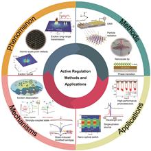
SignificanceIn the fields of modern information technology and optoelectronics, the exploration of new physical effects and their applications has become a key driving force for scientific and technological progress. As Moore’s law approaches its physical limits, it is particularly important to explore new materials and technologies that overcome the limitations of traditional semiconductor materials. Excitons, which are electrically neutral, hydrogen-like boson quasi-particles, are expected to combine the advantages of electrons and photons, thereby enhancing optoelectronic system interconnectivity. This makes them highly promising for next-generation optoelectronic devices. Two-dimensional (2D) transition metal dichalcogenides (TMDs) semiconductors, owing to quantum confinement and reduced dielectric screening, exhibit excitons with nanometer-scale Bohr radii and high binding energies (up to 500 meV). This facilitates device integration and room-temperature manipulation of excitons. Additionally, broken inversion symmetry and spin-orbit coupling in these materials introduce valley-spin degrees of freedom, offering new possibilities for information encoding and processing other than those based on charge and spin. Consequently, 2D exciton devices, such as circuits, switches, transistors, and sensors, based on semiconductor quantum well excitons, have garnered significant interest over the past decade.Typically, exciton dynamics in 2D materials are passively regulated into a steady state using fixed substrate patterns to modulate the surface of monolayer TMDs, or steady-state strain fields to alter the band structure and photoluminescence (PL) properties of the material. In contrast, active control enables real-time, dynamically customizable exciton manipulation through external fields such as electric fields, mechanical strain, or optical manipulation, allowing precise adjustment and real-time feedback.ProgressSurface acoustic wave (SAW) regulation is a method based on mechanical waves propagating along the surface of a solid to interact with 2D TMDs. By generating SAWs using interdigital transducers (IDTs), periodic piezoelectric and strain fields can be produced on 2D TMDs. These fields respond to the photoelectric properties of the 2D TMDs, thereby achieving dynamic regulation of exciton energy states and spatial positions (Fig. 2). The advantage of SAW regulation technology lies in its non-invasive, reversible, and real-time capabilities, enabling dynamic regulation without altering the intrinsic properties of the material. Particle irradiation introduces or regulates defects in TMDs using techniques such as ion irradiation, electron beams, gamma rays, neutrons, and lasers, significantly influencing the electronic and optical properties of the materials by creating atomic-scale defects. Specifically, these irradiation techniques introduce atomic-scale defects in 2D materials (Fig. 3), notably affecting the electronic and optical properties of the material (Fig. 4). Tip-induced regulation is a method that uses an atomic force microscopy (AFM) tip to precisely apply local strain to study and manipulate the dynamic behavior of excitons in 2D materials (Figs. 5‒7). By altering the strain state of the material, the bandgap of the material is affected, which then regulates its photoelectric properties. This method enables precise manipulation of exciton behavior in 2D TMDs at nanoscale and holds significant potential for the development of new optoelectronic and quantum devices. Phase transition regulation can cause variations in interface strain, electron density, and optical interference enhancement, which in turn affect the lattice vibration modes and PL emission intensity of the 2D TMDs semiconductor materials coated on top (Fig. 8). Phase transition regulation provides a new approach to control the physical properties of 2D TMDs without the need for chemical or mechanical treatment.Conclusions and ProspectsThis study explores active regulation techniques of excitons in 2D TMDs, including SAW control, particle irradiation, tip-induced strain control, and phase change regulation. These techniques significantly enhance the performance of TMD-based optoelectronic devices by precisely controlling the generation and recombination processes of excitons. Previous studies have shown that SAW control can achieve dynamic capture and transport of excitons; ionizing radiation techniques optimize the PL properties of materials by introducing defects; tip-induced strain control precisely manipulates the exciton behavior at nanoscale; phase change regulation affects exciton characteristics by altering the interfacial strain, electron density, and light field distribution. Despite significant progress in the active regulation of TMDs excitons, their short lifetime and limited mobility still restrict their long-range transport on a 2D plane. Therefore, fabricating high-quality monolayer TMDs semiconductor materials and optimizing the exciton transport mechanism remain hot research topics. Moreover, the precise construction of exciton transport paths depends on advanced micro-nano processing technologies. The development of high-precision and large-scale production-capable processing technologies is crucial for the commercialization and practical application of exciton devices. Likewise, a deeper understanding of the 2D exciton physical mechanism requires further exploration. Further research and technological innovations are necessary to overcome current limitations and promote the practical use of exciton technology in optoelectronics and beyond, driving device development in the post-Moore era.
Sep. 10, 2024Vol. 51 Issue 18 1801001 (2024)
Huifang Zhao, Zuohu Zhou, and Lei Zhang
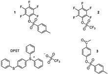
SignificancePhotoresist is a photosensitive material that exhibits changes in solubility upon exposure to light or radiation. Moreover, photoresist plays a key role in micro pattern processing in the field of microelectronics, which is characterized by high technological content, complex production processes, and long research and development cycles. Photoresist is widely used in flat displays, printed circuit boards, integrated circuits, microelectromechanical systems, and other fields. In the integrated circuit industry, the continuous development of photoresist materials provides an important guarantee for the continuation of Moore’s Law, and the continuous advancement of chip nodes puts higher requirements on the resolution of photoresist materials. Extreme ultraviolet (EUV) lithography is currently the most advanced chip manufacturing technology, and it is becoming increasingly prominent. Hence, the accompanying EUV photoresist is also receiving increased attention.ProgressFor an extreme ultraviolet light source, the photon corresponding to the wavelength of 13.5 nm for the radiation light has an energy of 92 eV, which is much higher than the ionization potential of the component atoms of the photoresist material. This leads to a significant difference in the reaction mechanism of extreme ultraviolet photoresist, compared with the previous generation of photoresists. Moreover, the glass transition temperature, thermal decomposition temperature, film-forming properties, extinction coefficient, refractive index, particle content, metal impurity content, and other parameters of the material also impact the performance of EUV photoresists. These factors make the development of extreme ultraviolet photoresists extremely challenging. To better promote the development of such key materials for integrated circuits, this study summarizes and discusses the latest domestic and international research progress on extreme ultraviolet photoresists. First, the research background and challenges faced by extreme ultraviolet photoresists are introduced. Then, a classification introduction is made from the perspectives of non-metallic and metal-based extreme ultraviolet photoresist materials. Four typical non-metallic EUV photoresists are presented: chemical amplification (Fig. 1), non-chemical amplification (Fig. 3), molecular glass (Fig. 7), and hydrogen sesquioxan (Fig. 9). Three metal-based EUV photoresists are presented: small metal-organic molecules (Fig. 10), metal oxides (Fig. 12), and metal oxo clusters (Fig. 13). A comprehensive summary and outlook are provided for the current technological route of metal oxide cluster type EUV photoresists, which has received widespread attention from both academia and industry. Overall, traditional organic photoresists, as represented by chemically amplified photoresists, are widely used in deep ultraviolet (DUV) and previous lithography technologies, and they show potential in EUV lithography applications. However, their inherent weak EUV photon absorption gives them a natural disadvantage in terms of EUV sensitivity. Correspondingly, introducing metal elements with high EUV photon absorption cross-sections can significantly improve sensitivity and reduce the output power requirements of EUV lithography machines, which are already extremely technologically complex. In addition, metal based EUV photoresists can enhance the etching resistance under low film thickness and thin lines, which is conducive to pattern transfer in advanced manufacturing processes.Conclusions and ProspectsConclusions and Prospects With the continuous development of EUV lithography technology, higher requirements are being put forward for EUV photoresists. In this context, various non-metallic and metal-based EUV lithography materials are reviewed, focusing on the latest research progress domestically and abroad. The results of a comparison of the lithographic performances of typical non-metallic and metal-based EUV photoresists indicate that metal-based EUV photoresists, especially metal oxo clusters, may become the mainstream technology route for the next generation of high-performance EUV photoresists. Research in this field has made good progress in recent years. However, considering the rich diversity and huge amount of known metal oxo clusters, research into their applications in EUV lithography is relatively limited, and the mechanism of solubility changes caused by photolithography reactions is still unclear. Therefore, it is crucial to develop new metal oxo cluster lithography materials using molecular design strategies. To achieve this goal, it is necessary to understand the inherent relationship between photolithography performance and the structures of metal oxo clusters. Therefore, lithography function-oriented structural design and the precise fabrication of metal oxo clusters are expected to greatly promote the development of EUV photoresists. In this process, the effects of metal cluster nuclei, coordination bonds between metals and ligands, and peripheral ligand layers on the performance of EUV lithography should be considered comprehensively.
Sep. 09, 2024Vol. 51 Issue 18 1801002 (2024)
Zhezhe Li, Jiangyong He, Jin Li, Shihai Wang, Congcong Liu, Yu Ning, Pan Wang, Yange Liu, and Zhi Wang
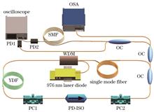
ObjectivePassively mode-locked fiber lasers, which are important for the development of fiber lasers, generate ultrashort pulses with wide spectral bandwidths and high peak power levels. They offer significant research value and are widely used in fields such as biosensing, communication, medicine, and military. The generation of dissipative solitons in these lasers requires a delicate balance among dispersion and nonlinear effects, gain and loss, spectral filtering effects of the gain medium, and saturable absorbers, thus rendering them an excellent platform for investigating nonlinear effects and soliton dynamics. Stimulated Raman scattering (SRS), which is a common nonlinear effect, has garnered widespread attention owing to its ability to significantly extend the wavelength range of ultrashort pulses. The development of time-stretch dispersive Fourier transform (DFT) techniques has enabled more dynamic soliton phenomena to be identified. Using DFT techniques, this study demonstrates double-soliton collisions in dissipative systems, as well as soliton collisions under SRS effects. The effect of SRS on the collision dynamics of solitons is demonstrated, thus expanding the study of nonlinear dynamic processes in soliton evolution dynamics.MethodsIn our experiment, we construct a ytterbium-doped passively mode-locked fiber laser with an entire laser cavity comprising positive-dispersion elements. We utilize a 50-cm-long ytterbium-doped fiber as the gain medium and exploit the birefringence filtering effect of the fiber as a filter. To provide a sufficient filtering bandwidth, we employ a 30-m-long single-mode fiber. A polarization-dependent isolator (PD-ISO) ensures the unidirectional transmission of pulses within the cavity and operates in conjunction with polarization controllers PC1 and PC2 to achieve nonlinear polarization locking. The cavity length is 40.5 m, with a net dispersion of approximately 0.99 ps2 and a repetition rate of 4.6114 MHz. We simultaneously measure the spectral, temporal, and real-time spectral characteristics using an optical spectrum analyzer, a high-speed oscilloscope, and DFT techniques. The dispersion required for DFT is provided by a 20-km-long single-mode fiber, which is a multimode fiber for the 1030 nm wavelength band, but higher-order modes can be effectively eliminated over long-distance transmission, thus ensuring reliable detection. The total dispersion is approximately 700.4 ps/nm. Using a fixed pump power, we successfully achieve dual-wavelength soliton collisions within a dissipative system by adjusting the polarization controller. Additionally, we achieve soliton collisions under Raman effects.Results and DiscussionsWe first analyze the results of soliton collisions in the absence of Raman effects (Fig. 3). By calculating the drift rate of the two solitons, we can determine that the collision is a dual wavelength soliton collision, and the corresponding transient evolution process is analyzed. The collision process shows pulses gradually approach each other until they overlap. After the overlap, the trailing pulse does not immediately vanish but continues to propagate before disappearing. Subsequently, the energy of the leading pulse increases, accompanied by broadening. After propagating for a certain duration, the pulse splits and drifts away from each other gradually, thus resulting in a decrease in the original soliton energy and an increase in the secondary soliton energy. Next, we illustrate soliton collisions under Raman effects (Fig. 5). The Raman effect influences the soliton collision, which causes both pulses to possess the frequency component of the main spectrum and the Raman-induced frequency-shift component. Consequently, the collision does not exhibit a significant relative drift, which is typically observed in conventional soliton collisions, owing to the approximate frequencies. Instead, constant pulse spacing is maintained during transmission. However, the frequency components of the two pulses are different, thus resulting in collision during propagation. Moreover, during the recovery after the collision, pulse reconstruction becomes difficult because of the partial energy gained by the Raman component during the collision, thus resulting in an unstable recovery.ConclusionsThis study presents the construction of a passively mode-locked ytterbium-doped fiber laser using a nonlinear polarization rotation (NPR) locking technique. Under certain pump power levels and polarization controller settings, soliton collisions are achieved and soliton collisions under Raman effects are reported. The differences between soliton collisions with and without Raman effects are elucidated to explain the influence of Raman effects on soliton collisions. The results of this study provide a clear understanding of soliton collisions and contribute to the understanding of the impact of Raman effects on complex nonlinear soliton dynamics. This understanding can further facilitate investigations into the potential applications of mode-locked fiber lasers.
Sep. 09, 2024Vol. 51 Issue 18 1801003 (2024)
Yifan Zhang, Zeliang Zhang, Pengfei Qi, Lu Sun, Nan Zhang, Lie Lin, and Weiwei Liu
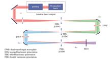
ObjectiveUltraviolet and deep-ultraviolet lasers offer short wavelengths and high photon energies. Thus, they are applicable to diverse fields such as fine processing, damage detection, and atomic spectral analysis. Deep-ultraviolet light-generation methods include synchrotron radiation, gas discharge lamps, excimer lasers, free-electron lasers, and nonlinear frequency conversion. Nonlinear frequency conversion uses nonlinear optical crystals to realize the output of deep-ultraviolet light via frequency doubling and frequency summing. Compared with other methods, it offers the advantages of low cost, simple structure, and continuous tuning. However, deep-ultraviolet lasers below 200 nm cannot be easily generated directly. Meanwhile, commonly used optical materials readily absorb deep-ultraviolet lasers, and the existing methods cannot offer both high efficiency and a wide tuning range.MethodsBy analyzing the coupled wave equation, the conversion efficiencies of the second, third and fourth harmonics in cascaded β?BBO crystals are discussed herein. The efficiency of nonlinear frequency conversion is positively correlated with the nonlinear polarization coefficient, and the nonlinear polarization coefficients of the third harmonic and above are much smaller than that of the second harmonic. Moreover, the shortest phase-matching range of the second harmonic of the β-BBO crystal is 409.6 nm, and the wavelength of deep-ultraviolet light is halted at 205 nm via direct frequency doubling. Therefore, we perform cascaded second-order nonlinear frequency conversion to achieve a high conversion efficiency for higher harmonics. The fundamental frequency light converges in the β-BBO crystal through the convex lens, and the second-harmonic wave perpendicular to the polarization direction of the fundamental frequency light is obtained. The two beams are collimated into parallel light using an off-axis parabolic mirror to avoid chromatic and spherical aberrations. After passing through a dual-wavelength waveplate (DWP), the polarization direction of the fundamental-frequency light rotates by 90°, the polarization direction of the second-harmonic wave remains unchanged, and the polarization direction of the fundamental-frequency light is the same as that of the second-harmonic wave. Subsequently, the fundamental frequency light and the second harmonic are converged in the second β-BBO crystal via an off-axis paraboloid mirror, whereas the third harmonic and fundamental frequency light are focused in the third β-BBO crystal via collimation and polarization adjustment, thus resulting in the fourth harmonic. Finally, a filter is used to filter the remaining wavelengths, and only the fourth harmonic is retained.Results and Discussions The simulation parameters are as followslaser output wavelength, 650?1050 nm; fundamental frequency power P0, 3.5 W; repeated frequency, 80 MHz; and pulse width, 150 ps. Additionally, fourth-harmonic crystal cooling to low temperature is performed to improve transmittance. The factors affecting the fourth-harmonic conversion efficiency are analyzed, and different crystal thickness conditions are simulated. The corresponding beam radius is calculated using the Rayleigh length formula, and a conversion-efficiency curve is obtained. The coupled wave equation is iterated step-by-step in the optical propagation direction using the Runge?Kutta method. Additionally, the beam radius and crystal thickness are obtained when the cascaded fourth-harmonic conversion efficiency is at its maximum. In practical application, the second-harmonic crystal length is 8.8 mm, the third-harmonic crystal length is 12.1 mm, the fourth-harmonic crystal length is 15.0 mm, and the laser radius is 33 μm (Fig. 5). The two-photon absorption coefficient of β-BBO crystal at 213 nm is 2.43 cm·GW-1, and the two-photon absorptivity of 15 mm long crystal is 6%, based on the simulation parameters. Under the fundamental optical condition with an output wavelength of 650?1050 nm and P0=3.5 W, the output power exceeds 100 mW in the range of 186?262.5 nm beyond the cascaded quadrupling frequency of the β-BBO crystal (Fig. 8). The maximum output power is 0.98 W at 227 nm, and the conversion efficiency is 28.6%. The results show that the cascaded output of the fourth harmonic of the deep-ultraviolet laser satisfies the requirements of wide tuning range and high conversion efficiency.ConclusionsBased on an analysis of the coupled wave equation, the conversion efficiencies of the second, third and fourth harmonics in cascade β-BBO crystals are discussed. The effects of beam radius, crystal thickness, and crystal temperature on the harmonic conversion efficiency are investigated. Additionally, the second-, third-, and fourth-harmonic conversion efficiencies and the fourth-harmonic conversion power at each wavelength are simulated. A fourth-harmonic power output exceeding 100 mW is obtained in the range of 186?262.5 nm, and the maximum conversion efficiency reaches 28.6% at 227 nm. The feasibility of a wide-range tunable ultraviolet light source is verified theoretically, and a reliable light-source scheme is provided for ultraviolet Raman-spectrum detection.
Sep. 10, 2024Vol. 51 Issue 18 1801004 (2024)
Jiahao Yang, Ruping Deng, Xianyou Wang, Yuquan Zhang, Xiaocong Yuan, and Changjun Min
SignificanceOptical tweezers are non-contact and high-precision particle trapping and manipulation tools that have been widely used in many scientific fields, such as physics, biology, and chemistry. However, traditional optical tweezers exhibit problems such as sample thermal damage caused by opto-thermal effects, which greatly limit the trapping ability and application range of samples. To solve these problems, opto-thermal tweezer technology has been proposed, which combines optical and heat effects for particle trapping and manipulation. Studies have shown that under certain conditions, the opto-thermal field can assist particle trapping through the optical heating or cooling effect of materials. Accordingly, various novel opto-thermal tweezer technologies have been proposed and developed. Compared with traditional optical tweezers, opto-thermal tweezers utilize the combined effect of optical and thermal fields to yield a lower laser power requirement, higher trapping accuracy, wider trapping region, and considerably reduced thermal damage of biomedical samples. To provide an overview and perspective on its development, this paper elaborates on the basic principle of opto-thermal tweezers, provides a detailed introduction to the development and application of some representative opto-thermal tweezer technologies, and discusses their future developmental prospects.ProgressOver the past decade, significant improvements and advancements have been achieved in the field of opto-thermal tweezer technology. Because most particles exhibit a “heat-averse” response to thermal effects, in 2018, Lin et al. proposed the concept of opto-thermoelectric nanotweezers. This involved the creation of a thermoelectric field within a solution by incorporating cetyltrimethylammonium chloride (CTAC), enabling the trapping of “heat-averse” particles (Fig. 3). In 2022, Wang et al. enhanced this technology by substituting an opto-thermal substrate with graphene, which possesses a much broader absorption spectrum. They also utilized a direct laser-writing technique to pattern the graphene substrate, achieving patterned traps and holographic manipulation of multiple particles (Fig. 4). To facilitate the application of opto-thermal tweezers in the biological field, in 2023, Chen et al. proposed a novel set of highly adaptable opto-thermal nano-tweezers that combines the principles of thermal penetration flow and dissipative force, where a dissipative force is used to trap various particles (Fig. 5). In 2021, Li et al. utilized the optical refrigeration effect for particle trapping. They employed laser irradiation on a ytterbium-doped yttrium lithium fluoride (Yb∶YLF) substrate to generate a localized laser cooling effect for particle trapping (Fig. 6). In 2023, Kollipara et al. invented a new type of hypothermal opto-thermophoretic tweezers that reverses the particle’s Soret coefficient by reducing the environmental temperature and utilizes laser irradiation of the substrate for opto-thermal trapping (Fig. 7). In 2022, Ding et al. proposed an opto-thermal manipulation method for light-driven micro/nanoscale rotors to achieve lateral rotation of particles along a direction perpendicular to the optical axis. By adding NaCl, PEG, and other reagents to the solution, they achieved a force balance at a specific distance from the light beam and provided lateral torque to the particles using an uneven charge distribution on the substrate (Fig. 8). In 2019, Li et al. successfully realized an opto-thermal control method capable of manipulating particles in air. They applied a thin CTAC layer onto glass and converted it into a quasi-liquid phase through laser irradiation using an optical scattering force to propel the particles (Fig. 9).The significant advantages of opto-thermal tweezers have been fully exploited in many fields such as materials science and biomedicine. In 2017, Lin et al. successfully achieved a low-power reconfigurable opto-thermoelectric printing technology using opto-thermal tweezers, enabling the printing and assembly of colloidal particles (Fig. 10). In 2022, Wang et al. utilized the highly efficient trapping ability of plasmonic-thermoelectric nano-tweezers for manipulating metal particles and combined it with a focused plasmonic enhancement effect to achieve super-resolution surface enhanced Raman spectroscopy (SERS) scanning imaging for two-dimensional material samples (Fig. 11). In the same year, Deng et al. manipulated silver nanoparticles into cells using graphene-based thermoelectric optical tweezers, which excited electromagnetic field hotspots and enabled in situ Raman spectroscopy detection at different positions within the cells (Fig. 12). In 2023, Chen et al. combined opto-thermal tweezer technology and clustered regularly interspaced short palindromic repeats (CRISPR) technology to propose an innovative CRISPR-driven opto-thermal nano-tweezer technology, which effectively aggregates biomolecules to meet the operational requirements of CRISPR technology (Fig. 13).Conclusions and ProspectsCompared with traditional optical tweezers, opto-thermal tweezer technology offers many advantages, such as a lower laser power requirement, higher trapping accuracy, stronger trapping force, and wider trapping region. These advantages enhance the performance of particle trapping and manipulation and significantly reduce the thermal damage experienced by the trapped sample particles. The development of opto-thermal tweezer technology has also included improved biocompatibility, and its application range has expanded to various fields. However, opto-thermal tweezer technology still faces challenges, particularly in the development of material substrates and surfactants and high-throughput large-scale particle manipulation. Despite these challenges, opto-thermal tweezers will be further developed as a major tool for particle trapping, and their application fields will continue to expand.
Sep. 10, 2024Vol. 51 Issue 18 1801005 (2024)
Hangjian Zhang, Boning Pang, Dahuai Zheng, Hongyun Chen, and Hongliang Liu
ObjectiveAs portable terminal devices become increasingly compact and lightweight in recent years, optical devices are gradually being miniaturized and integrated. However, conventional optical components based on lithium-niobate crystals are limited by their large optical volumes, which renders it difficult to satisfy the demand for the high-density integration of photonic chips; moreover, their further development is highly challenging. Breakthroughs in thin-film preparation technology offer a direction for overcoming these challenges. The lithium niobate-on-insulator (LNOI) platform provides the best comprehensive solution to address the long-standing low transmission loss, high-density integration, and low modulation power consumption requirements of photonic integrated chips, thus rendering it an ideal platform for photonic integrated chip technology. However, the current fabrication of photonic integrated devices based on the LNOI platform relies primarily on electron-beam lithography or ultraviolet lithography assisted by etching technology, which is characterized by complex fabrication processes, low processing efficiencies, and high processing costs. In this study, to investigate the potential application of femtosecond lasers in the fabrication of high-performance photonic integrated devices on an LNOI platform, we propose a method that uses femtosecond laser direct writing (FLDW)-assisted inductively coupled plasma (ICP) etching technology to fabricate Dammann grating structures on an LNOI platform.MethodsIn this study, the finite-difference time-domain (FDTD) method is used to guide the design of Dammann grating structures. First, the relationship between diffraction angle and grating period is obtained via simulation. Subsequently, the calculated parameters are introduced into the FDTD software as initial values for simulation optimization to determine the appropriate grating period and phase-transition point. For device fabrication, a layer of metallic chromium measuring approximately 600 nm thick is deposited on an LNOI platform using vacuum evaporation as a mask. FLDW is used to create a mask pattern of the Dammann grating on the chromium film. Subsequently, the mask pattern is transferred from the chromium film to the LNOI platform via inductively coupled plasma (ICP) etching. The expected depths of the Dammann gratings are obtained by varying the etching time. After removing the metal chromium film using a chromium etching solution, various Dammann grating structures are achieved based on the LNOI platform.Results and DiscussionsThe Dammann grating devices based on the LNOI platform fabricated via ICP etching exhibit high fidelity (Fig. 4), good anisotropic etching, and a high depth-to-width etching ratio (Fig. 5). The average etching depth of the grating is 250 nm and the grating exhibits good etching uniformity, thus satisfying the etching requirements. A 532 nm continuous laser is used as the excitation source inside the test system to characterize the diffraction performance of the grating structures (Fig. 6). The incident laser is expanded using a beam-expansion optical path composed of two lenses and then coupled to the surface of the Dammam grating through a small aperture. The output diffraction beam is obtained on the final charge coupled device (CCD) using an imaging objective lens to observe the intensity distribution of the light field diffracted by the Dammann grating. The test results show that the fabricated two-dimensional Dammann gratings can split beams effectively as well as diffract 2×2, 3×3, and 4×4 uniform light intensity arrays. The fabricated vortex Dammann grating is extremely efficient in generating a vortex beam and can diffract a 1×2 high-quality vortex beam array, which is consistent with the theoretical simulation result.ConclusionsIn summary, two-dimensional Dammann gratings and vortex Dammann grating devices are successfully fabricated on an LNOI platform via FLDW-assisted ICP etching. Compared with the conventional ultraviolet lithography or electron-beam lithography assisted by etching technology, mask-assisted etching technology using FLDW offers high processing freedom, good surface quality, a simple fabrication process, and high fabrication efficiency. Thus, it is extremely advantageous for the fabrication of large-scale high-performance micro-optical devices. This study demonstrates the potential of FLDW-assisted ICP etching technology for the fabrication of high-precision diffraction gratings on LNOI platforms, which can propel the development of high-performance photonic integrated devices on LNOI platforms.
Sep. 25, 2024Vol. 51 Issue 18 1801006 (2024)
Zhifang Wu, Yefen Wei, Jing Lin, Hupo Wang, Ruimin Huang, Xiaoyan Wang, and Jixiong Pu
Fiber-based curvature sensors, especially those capable of discerning the direction of curvature, have attracted more and more interest due to their promising applications in structural health monitoring, high-precision measurement, medical and biological diagnosis-treat instruments, and so on. Here, we propose and demonstrate a compact directional curvature sensor that comprises two bridged waveguides and three Bragg gratings in a section of three-core fiber (TCF). Both the waveguides and gratings are integrated by femtosecond laser micromachining method. The waveguides, connecting the TCF outer cores to the lead-in single-mode fiber core, function as beam couplers to realize simultaneous interrogation of all three gratings without any separate fan-in/out component. Owing to the spatial specificity, the outer-core gratings exhibit high and direction-dependent sensitivity to curvature, whereas the central-core grating is nearly insensitive to curvature but shows similar sensitivities to ambient temperature and axial strain as the outer-core gratings. It can be used to compensate the cross impact of temperature and strain when the outer-core gratings are applied for curvature detection. Moreover, the wavelength interval between two outer-core gratings is also proposed as an indicator for curvature sensing. It features with a much higher sensitivity to curvature and reduced sensitivities to temperature and axial strain. The corresponding maximum sensitivity to curvature is as high as 191.89 pm/m-1, while the sensitivities to temperature and strain are only 0.3 pm/℃ and 0.0218 pm/με, respectively. Therefore, our proposed device provides a compact and robust all-in-fiber solution for directional curvature sensing. It not only offers high sensitivity and accuracy but also immunity to temperature and axial strain fluctuations, making it a promising tool for a wide range of applications.
Sep. 18, 2024Vol. 51 Issue 18 1801007 (2024)
Wenzhe Chang, Yange Liu, Mao Feng, Xin Wang, Pan Wang, and Zhi Wang
SignificanceFew-mode long-period fiber grating (FM-LPFG), as a highly-integrated mode converter with few-mode fibers, has the advantages of high conversion efficiency, low insertion loss, strong robustness, simple fabrication, and inherent compatibility with fiber systems. These characteristics make it a highly promising candidate for a wide range of applications in optical communication transmission systems, fiber lasers, and optical sensors. In this study, the research progress of few-mode long-period fiber grating mode converter and its applications are summarized. We believe that this study is valuable for all researchers interested in FM-LPFG based devices and systems.ProgressIt has been more than 40 years since long-period fiber gratings were proposed. In contrast to single-mode long-period fiber gratings, researchers mainly focus on the conversion between the fundamental mode and core modes for FM-LPFG,which is achieved by satisfying the phase-matching conditions between the core modes in few-mode fibers. High conversion efficiency, low insertion loss, and wide bandwidth are the key performance indicators of FM-LPFG. The precision and efficiency of FM-LPFG have been significantly improved with the continuous advancement of fabrication technology, which has further inspired researchers to explore FM-LPFG with higher orders, wider bandwidths, and more channels. Significant progress and development have been achieved in these aspects. Researchers have proposed various techniques to fabricate FM-LPFGs, thereby achieving the generation of first- to fourth-order modes with high conversion efficiencies and low insertion losses, first- to third-order modes with a 15 dB bandwidth of more than 100 nm, and first- to fourth-order modes with multiple channels. These outstanding advances not only provide new perspectives and ideas for the research of FM-LPFG but also lay a solid foundation for the promotion of the development and application of related technologies.Conclusions and ProspectsThis study summarizes the research progress of a few-mode long-period fiber grating mode converter and its applications. First, the mode theory of few-mode fibers and the mode-coupling mechanism of long-period fiber gratings are introduced. Next, the characteristics and methods of the principal manufacturing techniques for few-mode long-period fiber gratings are described in detail. Subsequently, we focus on the progress in the development of higher-order, broadband, and multichannel few-mode long-period fiber gratings. A detailed summary is provided to introduce the applications of few-mode long-period fiber gratings in the fields of few-mode fiber lasers, sensing, and optical communication transmission systems. As the demand for high-capacity data transmission continues to grow, the development of new structures as well as high-performance and multifunctional few-mode long-period fiber gratings is expected to become an important direction of development for the new generation of fiber passive components.
Sep. 09, 2024Vol. 51 Issue 18 1801008 (2024)
Mingxia Ban, Zhaolin Chai, Manshi Wang, Nan Zhang, and Bing Liu
The dual-stage drilling scheme, i.e., first using polarization trepanning to process through holes and then using spinning beam to enlarge the hole diameter on the bottom surface, can process straight and inverted tapered holes with high efficiency. The experimental results show that this drilling scheme can decrease the processing time of straight hole by 17% compared with the conventional scheme.The quality of the holes affects the cooling efficiency of the blade film holes and the service life of the blades. Therefore, the roundness of the holes on the top and bottom surfaces must be further improved. During the processing, adding a circular mask with a diameter of 18 mm (Fig. 1) can effectively improve the roundness of the holes (Fig.7). Without using the mask, the holes roundness is significantly greater than 1. Using the mask, the hole roundness is approximately 1. An inverted tapered hole with a roundness of ~1, a diameter of 104 μm, an aspect ratio of 22, and a taper angle of -0.29° is successfully processed.ObjectiveHigh-aspect-ratio microholes are widely used in the film cooling of turbine-engine blades. The development of next-generation aviation turbine engines with higher thrust-to-weight ratios is an important topic related to national strategic security, and improvements to the thrust-to-weight ratio and efficiency rely on the further optimization of the engine intake temperature. Currently, gas film-cooling technology uses cooling holes with a diameter of ≥0.3 mm to form thermal protective gas films on the surface of hot components, and the cooling efficiency is typically less than 60%. The thrust-to-weight ratio of the next-generation aircraft engine can reach 15?20, which corresponds to an intake temperature greater than 2200 °C; thus, a cooling method that offers a higher cooling efficiency is necessitated. Studies show that film cooling holes with a diameter of ~100 μm and an aspect ratio of >20 can improve cooling efficiency significantly.MethodsLaser spinning is adopted in this study to process straight and inverted tapered holes with a diameter of ~100 μm and an aspect ratio of >20 on Inconel 718 alloy. The combination of polarization trepanning and spinning beam machining improves the drilling efficiency of the straight and inverted tapered holes (Fig. 1). A femtosecond-laser amplification system is used to output femtosecond-laser pulses with a center wavelength of 800 nm, a repetition rate of 500 Hz, a pulse width of 50 fs, and a maximum single pulse energy of 4 mJ. After passing through a tilted window and a half-wave plate, the femtosecond laser is focused onto the surface of the target material using a flat convex lens (L) with a focal length of 100 mm. The angle between the normal of the tilted window and the optical axis of the focusing lens is 15°. The target material used in the experiment is Inconel 718 alloy, with dimensions of 20.0 mm×20.0 mm×2.3 mm. The circular mask (aperture) at the exit of the laser amplifier is used to correct the cross-sectional profile of the femtosecond laser.Results and DiscussionsFigure 3(a) shows the dependence of the hole diameters on the top and bottom surfaces on the processing time of the laser-spinning drilling. As shown, the diameter on the top surface does not change significantly with time and remains 99?106 μm. Meanwhile, the hole diameter on the bottom surface increases as the processing advances. At the processing time of 3120 s, a straight hole with a diameter of ~100 mm and an aspect ratio of 22 is created. As the processing time increases to 3780 s, an inverted tapered hole with a taper angle of -0.17° is created.ConclusionsThis study proposes using spinning beam to process straight and inverted tapered holes with a diameter of 100 μm and an aspect ratio of >20. To improve the processing efficiency, polarization trepanning is first adopted to process through holes, followed by spinning beam to enlarge the hole diameter on the bottom surface. This dual-stage drilling method can reduce the processing time of a straight hole by 17% compared with the conventional method. By employing the circular mask to modify the cross-sectional profile of the femtosecond laser, an inverted tapered hole with a roundness of ~1, a diameter of 104 μm, an aspect ratio of 22, and a taper angle of -0.29° is successfully processed. The drilling method proposed herein can promote the application of high-aspect-ratio micro-holes in the fields of microelectromechanical systems (MEMS), engine fuel nozzles, and gas film-cooling holes.
Sep. 09, 2024Vol. 51 Issue 18 1801009 (2024)
Ailing Zhang, Ao Sun, Chaofan Zhen, Haozhe Chen, and Yanmei Shi
For the linear-cavity RFL, the pulse varies from a pulse-splitting state to a multi-period state as the modulation frequency increases (Fig. 10), whereas it varies from a multi-period state to a pulse-splitting state as the pump power increases (Fig. 11). P-22/1, P-6/1, P-3/1, and P-1/2 pulse states are obtained at modulation frequencies of 0.7, 2.0, 3.0, and 10.0 kHz, respectively, under a fixed pump power of 73 mW. P-1/2, P-3/1 and P-4/1 pulse states are obtained at pump powers of 73.0, 120.5, and 172.3 mW, respectively, under a fixed modulation frequency of 10 kHz. When an external laser with different wavelengths is injected, the number of pulses in one cycle increases with the pump power (Fig. 12), and its spectrum shows two lasing wavelengths (Fig. 13). In summary, the pulse evolution of the linear-cavity RFL is similar to that of the ring-cavity RFL. Regardless of the presence or absence of laser injection, as the pump power increases, the output pulses of the RFL transform from a multi-period state to a single-period state and then to a pulse-splitting state. Light injection does not fundamentally change the pulse evolution but only reduces the number of splitting pulses.ObjectiveOwing to the wide application of Q-switched random fiber lasers (RFLs) in numerous fields, such as medical and information encryption, the pulse characteristics and evolution of RFLs should be investigated comprehensively. Hence, the pulse characteristics and evolution of actively Q-switched random fiber lasers based on a random-phase-shift fiber Bragg grating (RPS-FBG) are investigated in this study. The pulse characteristics of the actively Q-switched RFLs with ring and linear cavities are compared. Results show that in the ring-cavity RFL, different pulse states such as multi-period, splitting, and chaotic pulses are obtained by adjusting the pump power and modulation frequency of the electro–optic modulator (EOM). In the linear-cavity RFL, pulse splitting and multi-period phenomena are similarly observed, which is consistent with the evolution of the ring-cavity RFLs. Moreover, external laser injection does not change the pulse evolution but only reduces the number of splitting pulses and generates a weak dark pulse.MethodsActively Q-switched RFLs with ring (Fig. 1) and linear cavities (Fig. 9) are investigated experimentally. The effects of pump power, EOM frequency, and external laser injection on the pulse characteristics of the RFLs and their evolution are analyzed. A photodetector (bandwidth of 200 MHz) and an oscilloscope (sampling rate of 2 GSa/s) are used to measure the pulse train of the RFLs, and an optical spectrum analyzer is used to characterize the RFL spectra.Results and DiscussionsFor the ring-cavity RFL, when the modulation signal is fixed, the output pulse is varied from a multi-period state to a single-period state and then to a pulse-splitting state with a chaotic state among different pulse-splitting states as the pump power increases (Fig. 3), while its spectrum remains relatively constant (Fig. 4). For example, the P-1/2 state is achieved at a pump power of 50 mW, whereas the P-1/1 state is obtained at a pump power of 80 mW. At pump powers of 140, 200, 240, and 270 mW, the pulse state evolves sequentially into the P-2/1, P-3/1, P-4/1, and P-5/1 states, respectively. When the pump power is fixed, the pulse varies from a pulse-splitting state to a multi-period state as the modulation frequency increases (Figs. 5 and 6), whereas its spectrum remains relatively constant (Fig. 7). For example, P-5/1, P-3/1, P-2/1, P-3/2, P-3/2, and P-1/1 pulse states are obtained at modulation frequencies of 1, 2, 3, 4, 5, and 6 kHz, respectively (Fig. 5); P-1/2, P-1/3, and P-1/4 pulse states are obtained at 19, 23, and 31 kHz, respectively; and P-1/4, P-1/3, P-1/2, and P-1/1 pulse states are obtained at 36, 48, 56, and 62 kHz, respectively (Fig. 6). In other words, the pulse characteristics and evolution of the multi-period, splitting, and chaotic pulses in the ring-cavity RFL vary with the pump power and modulation frequency, as shown in Fig. 8.ConclusionsThe experimental results indicate that the pulse parameters can be controlled by adjusting the pump power and modulation frequency under multi-period, splitting, and chaotic pulse states in both actively Q-switched RFLs with ring and linear cavities. Moreover, the pulse evolution with pump power and modulation frequency is highly consistent. External laser injection reduces the number of splitting pulses and generates weak dark pulses. In summary, the pulse characteristics of actively Q-switched RFLs based on an RPS-FBG are determined by the pump power, modulation frequency, and external injection. These RFLs are promising for applications in biological simulations and encrypted communication.
Sep. 25, 2024Vol. 51 Issue 18 1801010 (2024)
Zhen Xu, Bohan Liang, Longhai Liu, Man Luo, Jining Li, Kai Zhong, Yuye Wang, and Degang Xu
ObjectiveMicrostrip circuits are typically used to combine devices and circuits to improve the overall performance of a machine. They offer advantages of high reliability and integration; however, their cumbersome and complex processing process can easily cause breakage, bending, branching, and other inhomogeneity problems, thus causing adverse equipment operations. The classical microstrip-circuit defect-detection methods involve complex image post-processing, difficult to distinguish high-density alignments, long test cycles, and other shortcomings. Hence, a more efficient and convenient detection technology that can localize fault defects is required.MethodsTime-domain reflection is a technique that involves injecting a pulse signal into a test sample, and the impedance-change position in the line will reflect a portion of the pulse signal. The type and location of impedance change can be determined based on the peak characteristics of the reflected signal. The classical pulse time-domain reflection technique features large signal jitters and low resolutions, whereas the rise time of terahertz pulses is on the order of picoseconds and the signal jitter is on the order of femtoseconds. Applying terahertz pulses in the time-domain reflection detection of defects in microstrip circuits allows one to detect defects with high resolution and accurate localization. In this study, different lengths of microstrip wires, different numbers of branching wires, and “back” bent wires were designed to simulate three different types of inhomogeneous structures typically observed in broken wires, T-branches, and continuous right-angle bending microstrip circuits, respectively. First, the terahertz pulse time-domain reflection signals of the three different types of inhomogeneous wires were obtained using the ADVANTEST TS9001TDR system, and the distance error between the inhomogeneous position calculated based on the pulse signals and the actual position was analyzed. Subsequently, simulation software was used to establish a pulse time-domain reflection model for the inhomogeneous microstrip wires. Finally, the theory of equivalent-circuit models was utilized to analyze equivalent circuits corresponding to the different types of inhomogeneous structures, based on which the occurrence mechanism of pulse reflection-signal characteristics was explained.Results and DiscussionsFor different lengths of open wires, the upward positive pulse signal is reflected back to the location of the open-circuit fault. When the wire length is relatively short, the pulse signal is reflected multiple times between the test point and the fault location and gradually attenuates to 0. Meanwhile, the second and third reflection signals, which are two, four, and eight times the length of the wire of the first pulse time-domain reflection signal, coincide with the first reflection signal (Fig. 6). When the length of the wire is 50 or 100 mm, at the branch position of the wire, reflected signal with a peak downward will be generated. When a terahertz pulse signal is transmitted to the end of the wire, it is reflected back as an upward positive peak. Additional pulse signals are reflected when multiple branches exist; however, the fewer the number of branches, the more significant are the corresponding pulse time-domain reflection signals (Figs. 7 and 8). When multiple consecutive bends exist in the wire, negative pulse signals are reflected back at the bend locations, and the farther the bend location is from the test point, the weaker is the reflected signal (Fig. 9). Experimental results show that for the three different types of inhomogeneities, the greater the number of inhomogeneous locations on the wire and the longer the pulse transmission distance, the greater is the error (Fig. 10a). This is attributable to the experimental operation and the low precision of sample processing. The peak change states of the reflected signals in the time domain obtained from the simulation of the three different types of microstrip-circuit inhomogeneity models are consistent with the experimental results. Theoretical analysis shows that when a bend or T-branch occurs in the microstrip line, charges accumulate therein, which is equivalent to an increase in the capacitance, i.e., a decrease in the characteristic impedance, thus causing the reflection coefficient to be less than 0. Meanwhile, the reflection signal is shown as a downward reflection signal in the time domain, i.e., negative peaks at the location of impedance change, which is consistent with the experimental and simulation results.ConclusionsThe results show that the minimum errors between the impedance-change location calculated from the pulse correspondence time and the actual inhomogeneity-occurrence location are 1.2%, 0.2%, and 1.4%, and that a distance error of 10 μm can be detected. The terahertz pulse time-domain reflection technique can discriminate the type of microstrip-line inhomogeneity and locate it accurately; however, the detection effect for multiple inhomogeneities on the same microstrip line must be further optimized. Microstrip circuits, as a key device in radio equipment and modern integrated systems, contribute significantly to the rapid detection of microstrip-circuit wire inhomogeneity, thus providing a foundation for the research of more efficient detection of defects inside packaged chips.
Sep. 09, 2024Vol. 51 Issue 18 1801011 (2024)
Xiaoqin Meng, Ye Tong, Yan Xu, and Zhen Chai
SignificanceOptically pumped magnetometers (OPMs) are crucial in magnetic-field measurements. Its high sensitivity and low noise allow it to detect weak magnetic-field changes up to the nT level, thus significantly expanding human understanding into the micro-magnetic-field environment. OPMs are beneficial in various areas, including the precise mapping of Earth’s magnetic field, the detection of weak biological magnetic signals within biological tissues, quantum computing, and magnetic-material research.The main function of an OPM is to detect magnetic fields using specific polarized pump light and detection light. High-purity pump light, which is typically linearly or circularly polarized, interacts with atomic cells. The selective excitation of pump light causes the arrangement of atomic magnetic moments to align with the polarization direction of light, thus forming a magnetized region. This process is known as optical pumping, which effectively places atoms in specific magnetic quantum states, thereby enhancing their sensitivity to magnetic fields. This allows the detection of light passing through magnetized regions with different polarization states. Under the effect of a magnetic field, the energy levels of atoms undergo Zeeman splitting, which affects the absorption and scattering of detection light. By analyzing and detecting changes in light intensity or polarization rotation, the intensity and direction of the magnetic field can be inferred accurately. The polarization state must be controlled precisely as it determines the manner by which atoms are excited and their response to magnetic fields, thereby ensuring the high sensitivity and measurement accuracy of the equipment. This principle based on atomic magnetic resonance renders the OPM an ideal tool for detecting weak magnetic fields; thus, OPMs are widely used in scientific research and practical applications.Aided by the development of modern technology, researchers have comprehensively investigated vector lights with complex polarization states and gradually applied them to OPMs. In an OPM, particularly the component involving the interaction between vector light and atoms, dichroism and birefringence are two key optical phenomena. Dichroism refers to the different propagation characteristics of light in different polarization directions. This characteristic is used to selectively excite or manipulate atoms of specific energy levels in an OPM. Birefringence refers to the difference in the refractive index between vertically and horizontally polarized light in a medium, which causes a beam to separate when it passes through an atomic medium. By leveraging the properties above and examining the practical application of vector light in OPMs, we can further improve the sensitivity of OPMs. Compared with conventional OPMs, a new type of OPM based on vector light pumping/detection features rapid response, adaptability to more complex environments, and high sensitivity. Owing to the vector characteristics of vector light, this OPM can simultaneously measure multiple components of the magnetic field, thus achieving complete magnetic-field vector measurements without requiring additional optical paths. Therefore, it is more suitable for integration into complex optical systems in fields such as biomedical, material science, and space exploration.ProgressThis paper summarizes the development history of OPMs, describes their operating principle (Figs. 2 and 3), and explains the energy-level transition of optically pumped polarized alkali metal atoms based on a 87Rb atomic energy-level diagram (Fig. 4). As per the development history of OPMs, optical polarization is crucial to the entire process (Fig. 5). Vector light is a new type of beam that has emerged in recent years, and its polarization state is distributed in a certain pattern on the cross-section of the beam (Fig. 6). The measurement of vector light in a magnetic field has been investigated extensively (Fig. 7). In terms of light and matter, investigating the dichroism and birefringence in the interaction between vector light and alkali metal atoms is crucial for OPMs. Based on dichroism, when a beam of linearly polarized light is irradiated onto an alkali metal atomic-gas chamber, the absorption and scattering efficiency of light varies owing to the ultrafine structure of the atoms and the energy levels of different magnetic quantum numbers. By adjusting the polarization direction of light, atoms can be more effectively pumped into specific magnetic states, thereby enhancing their response to magnetic fields (Fig. 8). Based on birefringence, vector light is incident in the orthogonal pumping direction, and the relationship between the polarization rotation angle of the detected light and the external magnetic field after the light passes through the gas chamber can be derived (Fig. 9). In practical applications, vector light with complex polarization states can be used as pump/detection light not only for the real-time dynamic detection of the magnetic-field size (Fig. 10) but also for solving the “dead zone” problem in magnetometers, improving spatial resolution and sensitivity (Fig. 11), and achieving miniaturized OPMs.Conclusions and ProspectsComprehensive investigations into quantum optics and the development of micro- and nano-technology will refine the manipulation of vector light, which is expected to enable magnetic-field measurements with higher sensitivities and resolutions. New OPMs based on vector optical pumping/detection have gradually received the attention of researchers. Thus, the application of OPMs in biomedicine, geological exploration, quantum information processing, and other fields will be promoted. Additionally, the miniaturization and integrated design of OPMs render them more portable and will further broaden their practical use. In the future, the development of vector-light technology will significantly improve OPMs.
Sep. 09, 2024Vol. 51 Issue 18 1801012 (2024)
Mingming Luo, Caiyun Wang, and Jianfei Liu
SignificanceRayleigh scattering usually occurs at sub-wavelength scaled particles in an imperfect optical waveguide. The localized and unique “finger-print” like Rayleigh scattering spectrum could be used for spatial positioning and recognition. While the Fresnel reflection arises at the interface with a refractive index gradient, carrying the optical waveguide performances within the entire fiber segment. Moreover, the signal-to-noise ratio of the Fresnel probe light is much higher than that of the Rayleigh light, as the intensity of Fresnel reflection is 3‒4 orders higher than that of the background Rayleigh scattering. Thus, the optical fiber can be measured and characterized with the Rayleigh scattering and Fresnel reflection using polarized coherent optical frequency domain reflectometry (OFDR).OFDR, born from frequency modulated continuous wave (FMCW), was first utilized for fault positioning and diagnosis in all-fiber network. Thereafter, an auxiliary Michelson interferometer consisting of two Faraday rotation mirrors was used to calibrate scanning nonlinearity of the tunable laser source (TLS). Thus, its spatial resolution was improved to millimeter level within tens of meters. Besides, dual-polarization harvesting is also used for polarized intensity maintenance, where the spectral correlation along the fiber is free from the zero signals caused by orthogonal reference and measurement paths.In recent years, the improved dual-polarization coherent OFDR system was applied in different scenarios including extremely high/low temperature monitoring, large range of strain measurement in structuring engineering, as well as the mode group recognition and waveguide characterization. Particularly, mode groups in a few-mode optical fiber was further discussed with their appearances one by another, in which their differential mode delay can be quantified by the frequency difference between the Fresnel reflection peaks. Moreover, birefringence was measured and calculated in a dual-air-hole microstructured optical fiber using OFDR as well, with the result close to that given by the manufacturer. Additionally, the birefringence can also be regulated and observed by OFDR where two polarized modes exchange their group velocity at the zero points in frequency domain. The OFDR promises a good prospect in high-resolution distributed optical fiber sensing and waveguide characterization.ProgressA dual-polarization harvesting coherent OFDR was proposed and demonstrated as a sub-millimeter spatial resolution distributed optical fiber temperature and strain sensor. The 0.5 mm spatial resolution was not only calculated in theoretical analysis but also verified in experiment with deliberately introduced small scaled optical fiber segments with different axial strain distribution [Fig. 3(d)]. The high temperature monitoring was achieved from room temperature to 500 ℃ using a 23 m gold coated optical fiber [Fig. 4(a)]. The wind energy research group of the United States Department of Energy measured the strain distribution along the loaded CX-100 wind turbine blade, locating the fatigue area after repeated loading [Fig. 5(a)]. The OFDR distributed strain sensor was embedded in a reinforced concrete of a bridge over the Black River in Canada, where the loads were clearly recognized with the strain distribution [Fig. 5(b)]. Compared with S2 method as well as the low coherent interferometry, OFDR stands out for its high contrast and mode separation in frequency domain. Thus, the mode excitation from LP01 mode to LP12 mode in turn was observed and characterized in a 6.6 m six-mode optical fiber (Fig. 7). The demonstration provides a feasible and flexible method for mode group identification and characterization of all kinds of fibers. Similarly, LP01 mode to LP11 mode were observed in a dual-mode fluorine-trench optical fiber, and their differential mode delay can be realized by the beat frequency difference between two Fresnel peaks (Fig. 8). A special hybrid mode was found just between the two Fresnel peaks, which may be regarded as the mode convention at the optical fiber end. The birefringence in a dual-hole microstructured optical fiber was numerically calculated and characterized with an OFDR method (Fig. 10). Due to the asymmetric dual air-holes in the cross section, the polarized LP01X and LP01Y modes propagate with different group velocities and time delays. The group birefringence of -9.68×10⁻⁴ was obtained with a beat frequency difference of 50.03 Hz, which was in good agreement with that given by numerical analysis. Moreover, the birefringence could be further regulated with selective infiltration using a functional material with a high thermal-optic coefficient. Due to the co-effects of the filled and unfilled fiber segments, the twin critical zeros of the overall group birefringence were observed at 16.5 and 43.0 ℃, respectively (Fig. 11). The unique position exchange of LP01X and LP01Y presents at the twin critical zeros, which has been investigated via the OFDR technique as well.Conclusions and ProspectsThe OFDR technique is briefly reviewed in this paper with improved processes using hardware and software methods. This technique with excellent performances is applied not only in high-resolution sensing, but in waveguide measurement and characterization as well. Rayleigh scattering and Fresnel reflection in optical fibers carry abundant information, which are capable of characterizing mode components, purity, group velocity, birefringence in time/spatial/frequency domain. With an induced Fresnel reflection surface at a hollow-core fiber end, the OFDR method is also suitable for hollow-core microstructured optical fibers. The OFDR method promises possibility for group velocity measurement in hollow-core fiber close to that in vacuum as a compact high-resolution optical instrument.
Sep. 09, 2024Vol. 51 Issue 18 1801013 (2024)
Peng Wei, Yuehui Ma, Siyu Chen, Xiaolong Fan, and Yunqi Liu
ObjectiveFew-mode fiber (FMF) components can fully utilize multiple spatial modes to achieve multiparameter measurements while offering high accuracy and detection efficiency; thus, they are widely used in optical communications and fiber sensors. This study investigates long-period fiber gratings (LPFGs) inscribed in a tapered FMF with different waist diameters, both numerically and experimentally. The mode coupling, polarization-dependent loss, temperature, refractive index, and torsion characteristics of the tapered FMF-LPFGs with different waist diameters were investigated experimentally. The experimental results show that the torsion sensitivity of the core mode can be improved, whereas the refractive-index sensitivity and the torsion sensitivity of the cladding mode increase significantly, with maximum values of 12166.7 nm·RIU-1 and 0.72 nm·rad-1·m achieved, respectively, as the waist diameter decreases. The tapered FMF-LPFGs can be applied as a high-sensitivity refractive-index sensor and torsion sensor for fiber sensing.MethodsIn this study, we change the diameter of an FMF via fiber tapering and fabricate LPFGs in the tapered FMF using carbon-dioxide laser. We use the COMSOL Multiphysics simulation software to calculate the propagation modes and effective refractive indices supported by the FMF with different waist diameters in different wavebands. Based on phase matching, we plot the phase-matching curves for different modes of the tapered FMF-LPFGs. The fundamental mode is coupled to the higher-order core modes in the FMF with a larger waist diameter, whereas it is coupled to the cladding mode in the FMF with a smaller waist diameter. By reducing the waist diameter, the sensitivity of higher-order core modes and cladding modes can be improved.Results and DiscussionsWe fabricated tapered FMFs with different waist diameters using a carbon-dioxide laser glass-processing system. Subsequently, the LPFGs with different periods were inscribed in the tapered FMFs with different waist diameters using a carbon-dioxide laser. We observed the mode field distribution of the tapered FMF-LPFGs. The resonance wavelength and mode field distribution are consistent with the simulation results, as shown in Figs. 1 and 2. The tapered FMF-LPFG presents a lower polarization-dependent loss and temperature sensitivity. Figure 7 shows the refractive-index characteristics of the LP12 cladding mode. As the waist diameter decreases, the refractive-index sensitivity increases significantly. Figures 8, 9, and 10 show the torsion characteristics of the LP11 and LP21 core modes and the LP12 cladding mode, respectively. As the waist diameter decreases, the torsion sensitivities of the three abovementioned modes improve significantly.ConclusionsThe three core modes and the cladding mode can be excited by the tapered FMF-LPFGs. The refractive-index sensitivity and torsion sensitivity of the cladding mode can reach 12166.7 nm·RIU-1 and 0.72 nm·rad-1·m, respectively, which can benefit fiber sensing. Therefore, the proposed tapered FMF-LPFG can be used as a high-sensitivity refractive-index sensor and torsion sensor.
Sep. 06, 2024Vol. 51 Issue 18 1801014 (2024)
Yao Yao, Yangjun Mei, Li Lao, and Jiayu Zhao
In addition, the octagonal tube exhibits the lowest loss, whereas the circular and square tubes show slightly higher losses. This can be attributed to the fact that the octagonal tube combines the advantages of both circular and square tubes. First, the geometric shape matching between the input terahertz beam profile and the waveguide tube cross section is crucial. Considering that the terahertz Gaussian beam enters the waveguide tube and diverges from the center point before being reflected by the tube walls, an ideal cross section would be circular. In this case, all rays would reach the tube wall simultaneously and return to the origin, maintaining synchronization throughout the propagation along the waveguide. By contrast, for polygonal tubes with non-circular cross sections, the geometric shape mismatch leads to imperfect synchronization of the rays, with fewer sides resulting in poorer synchronization. Second, the core-antiresonance effect is generated by the oscillation of transverse electric (TE) polarized light between the waveguide’s tube walls. For a circular tube, the opposing tube walls are theoretically only two infinitesimal points within its cross section. However, in a polygonal tube, the opposing walls are much broader. Accordingly, polygonal tubes have an advantage over circular ones. The octagonal tube benefits from both aspects, which is the primary reason for its lower transmission loss. Moreover, the loss is reduced when the tube walls are made of magnetic paper than of ordinary paper. This is mainly because magnetic paper has a higher reflectivity for terahertz waves.Regarding the uncertainties associated with the octagonal tube and U-shaped tube devices, the former primarily derives from material fatigue induced by repeated deformations of the octagonal origami structure under magnetic force. Over time, the tube may struggle to return to its initial regular octagonal shape, leading to a gradual decline in the control accuracy and stability of the terahertz polarization state. By contrast, the U-shaped tube offers better stability, as the magnetic paper only needs to lift or lower under the influence of the magnetic field. However, environmental humidity can alter the elasticity and toughness of the paper, potentially reducing the device’s precision in controlling the terahertz polarization state. A future work will address these issues. Specifically, we will experiment with plastic magnetic materials to enhance the control accuracy and stability of the devices.Future research should focus on further optimizing the structural parameters and performance of these terahertz polarization conversion waveguides. In addition, exploring alternative control methods beyond magnetic fields, such as thermal and temperature control, is essential to meet the diverse requirements for terahertz polarization modulation under various scenarios.ObjectiveIn recent years, terahertz technology has garnered widespread attention and experienced rapid development. Among the key research areas in this field, terahertz polarization control is one of the most significant, as it holds broad application prospects in terahertz imaging, sensing, communication, and radar. Consequently, the efficient manipulation of terahertz polarization states has become a major focus of current research. Although many terahertz polarization conversion devices offer diverse control capabilities, they face challenges in terms of device fabrication complexity, terahertz wave losses, and the ability to continuously modulate polarization states. For example, terahertz polarization converters based on metasurfaces are difficult to fabricate and involve complex manufacturing processes. In addition, these devices often experience significant terahertz losses. In reflective polarization converters, the terahertz wave transmission efficiency can vary from 50% to 80%. More importantly, because most terahertz polarization control devices have a fixed wavefront modulation phase once they are fabricated, they are typically limited to switching between two specific polarization states, such as from linear to circular polarization. Consequently, they often lack the ability to achieve continuous polarization state control.MethodsTo address the aforementioned challenges, this study innovatively proposes a magnetically controlled terahertz polarization conversion waveguide based on the antiresonance mechanism of the waveguide core. The study first utilized magnetic paper and 3D printing technology to fabricate octagonal paper tube waveguides and U-shaped tube waveguides, which transmit terahertz waves via a core-antiresonance mechanism. Then, when a magnetic field was applied near the output port of the waveguide, the orthogonal inner diameters of the waveguide underwent relative changes. Finally, these changes in the orthogonal inner diameters led to variations in the relative time delay of the orthogonal terahertz polarization components as they propagated through the tube.Results and DiscussionThe results of this study show that the hollow-core waveguide device is capable of controlling terahertz polarization, thus offering several advantages: 1) the waveguide structure and fabrication process are simple; 2) the terahertz wave transmission loss is low; 3) continuous control of the terahertz polarization state can be achieved; 4) the proposed polarization conversion method is flexible. In addition to magnetic control, replacing the magnetic paper with ordinary paper or 4D printed materials allows polarization adjustment through force or thermal control.ConclusionsTo address the challenges of complex fabrication processes, low transmission efficiency, and difficulty in achieving continuous adjustment in terahertz polarization converters, this study innovatively proposes two types of magnetically controlled terahertz polarization conversion waveguides based on the core-antiresonance transmission mechanism. These devices can be fabricated using simple origami techniques or 3D printing, where transmission losses are as low as 0.04 cm-1 at peak frequencies. They also enable continuous adjustment and chirality switching among the three polarization states of linear, elliptical, and circular polarization under an applied magnetic field.
Sep. 06, 2024Vol. 51 Issue 18 1801015 (2024)
Yongfang Zou, Xinyong Dong, Zhikai Wu, Jianxiang Wen, Tingyun Wang, Song Wang, Yuncai Wang, and Yuwen Qin
To investigate the role of LPG in a high-gain EDFA with full coverage in the C+L band, the gain and noise are tested in two separate scenarios, with and without an LPG inserted between ports 1 and 3 of circulator 2. These two structures are referred to as “comparison structure 1” and “comparison structure 2,” respectively. The amplifier structure (shown in Fig. 1) is designated as the “reported structure.”ObjectiveIncreasing the gain bandwidth of optical fiber amplifiers is the simplest and most effective method for improving the transmission capacity of optical fiber communication systems. Currently, C+L-band erbium-doped fiber amplifiers (EDFAs) are typically formed by parallel C- and L-band EDFAs, without any gaps between the two bands. Therefore, the research and development for an EDFA with a high gain bandwidth that fully covers the C+L band, have always garnered attention. However, the initially designed C+L band EDFA either fails to cover the gain bandwidth within entire C+L band or suffers from low gain levels and high noise, unable to fully meet the requirements of long-distance transmission systems. In this study, a C+L-band full-coverage high-gain EDFA is realized using a Bi/Er co-doped fiber as the main gain medium in a two-stage double-pass amplification structure with a long-period fiber grating inserted to shave the gain peak and fill the valley with 25 dB and 20 dB gain bandwidths corresponding to 78 nm (1529?1607 nm) and 85 nm (1527?1612 nm), respectively. The maximum gain reaches 51.2 dB, and the minimum noise is 3.9 dB, achieving a sufficiently high gain in a broad gain bandwidth covering the entire C+L-band, indicating a high potential for widespread use in future high-capacity long-haul optical fiber transmission systems.MethodsTo increase the gain level and control noise, the amplifier uses a two-stage double-pass amplification structure. The main amplifier has an 8 m long bismuth/erbium co-doped silica fiber (BEDF ) as the gain medium, which is bidirectionally pumped by a pair of 1480 nm laser diodes. The BEDF is fabricated using the atomic layer deposition (ALD) method in conjunction with modified chemical vapor deposition (MCVD). In addition to the co-doped elements of Bi (mole fraction of 0.004%) and Er (mole fraction of 0.109 %), Al, P, and Ge are also included. This fiber exhibits a background loss of 0.02 dB/m at 1200 nm and an absorption coefficient of 22 dB/m at 1531 nm. For the pre-amplifier, a 2 m high-concentration EDF is used as the gain medium, which is forward pumped by a 980 nm laser diode (LD) with a pump power of 100 mW. A fiber ring mirror consisting of an optical circulator (circulator 2) is connected at the end of the main amplifier, which is used to route the amplified input signals and the forward-amplified spontaneous emission (ASE) back into the amplifier system to achieve double-pass amplification. The gain bandwidth is expanded by inserting a wavelength-matched long-period fiber grating between the main amplifier and fiber ring mirror.Results and DiscussionsThe experimental results on measurement gain and noise of the three EDFA structures under the same experimental conditions are displayed in Fig. 4. Clearly, the gain spectra of all three amplifier structures cover the C+L band region, extend to 1620 nm on the long-wavelength side, and provide a broader wavelength range than conventional EDFAs. Additionally, the gain level in the L-band, which is closely related to the broad-spectrum gain characteristics of the Bi/Er co-doped fibers, is enhanced. Among the three structures, the reported structure for the amplifier exhibits a significantly broader gain bandwidth than those of structures 1 and 2. Specifically, the 25 dB and 20 dB gain bandwidths reach 78 nm (1529?1607 nm) and 85 nm (1527?1612 nm), respectively, fully covering the entire C+L band. In terms of noise performance comparison, all three structures maintain a relatively low noise of below 6 dB within the wavelength range of 1545?1608 nm. This is primarily attributed to the incorporation of a preamplifier because the noise of the two-stage amplifier architecture is predominantly determined by the noise of the first-stage amplifier. Compared with the main performance parameters of C+L-band EDFAs reported in recent years (Table 1), the C+L-band EDFA demonstrated in this study exhibits the best comprehensive performance: a high gain level, low noise, and a 25 dB gain bandwidth that completely covers the C+L-band.ConclusionsUsing Bi/Er co-doped silica fiber as the primary gain medium and a two-stage double-pass amplification structure, this study employs long-period fiber gratings to expand the gain bandwidth. Consequently, a high-gain erbium-doped fiber amplifier with full coverage of the C+L band is achieved. The 25 dB and 20 dB gain bandwidths reach 78 nm (1529?1607 nm) and 85 nm (1527?1612 nm), respectively, with a maximum gain of 51.2 dB and minimum low noise of 3.9 dB. Compared with the Bi/Er co-doped fiber C+L band EDFA reported in recent years, this amplifier not only exhibits high gain and low noise but also achieves full coverage of the C+L band with 25 dB gain bandwidth. Its superior overall performance is expected to lead to important applications in future high-capacity long-haul optical fiber transmission systems.
Sep. 09, 2024Vol. 51 Issue 18 1801016 (2024)
Jie Lin, Ji Qi, Yuqi Zhang, Wei Zhang, Yuang Chen, Mingxia He, Qiuhong Qu, and Yizhu Zhang
Following layer classification, the Rouard model was applied to globally fit each layer’s thickness. This model, coupled with the genetic algorithm for parameter optimization, enabled accurate thickness determination even when the number of layers was initially unknown. The genetic algorithm iteratively adjusted the model parameters to minimize the difference between the measured and calculated THz signals. The feasibility and effectiveness of the proposed method were validated through experiments on curved multi-layer samples using a robotic arm-driven THz-TDS system.The THz-TDS system employed in experiments was shown to be capable of high-resolution measurements, covering a broad spectral range. The robotic-arm integration allowed for precise positioning and orientation of the THz probe, ensured accurate data collection from curved surfaces. This setup mimicked real-world industrial applications in which components often had complex geometries.The THz reflection data clearly depict the distinct characteristics of different layer structures. The layer thickness measurements using the Rouard model are highly accurate, with the first, second, and third layers of paint averaging (47.93±5.81) μm, (98.86±0.57) μm, and (57.20±0.79) μm, respectively. These measurements are consistent with the actual thickness values obtained using an eddy current thickness gauge.The KPCA-ISSA-SVM model also demonstrates robustness and efficiency in classifying the number of layers, which is crucial for subsequent thickness measurements. The improved classification and measurement accuracy underscore the potential of the proposed method in industrial applications in which precise and non-contact thickness measurements are required.The optimization of SVM parameters using advanced algorithms such as ISSA and WOA significantly improves the model’s ability to classify the number of layers accurately. The inclusion of KPCA for feature extraction from the THz spectral data enhances the model’s performance by reducing dimensionality and focusing on the most informative features. This combination of techniques results in a highly accurate and efficient classification model that can be applied to various industrial scenarios requiring precise layer thickness measurements.The experiment demonstrates the method’s capability in handling complex multi-layer structures on curved surfaces, which is a common challenge in practical applications. The robotic arm-driven THz-TDS system provides a versatile platform for accurate and repeatable measurements, further validating the method’s practicality and effectiveness. The system’s ability to adapt to different surface geometries and layer configurations highlights its potential for widespread industrial adoption.The study explores the effects of different optimization algorithms on the classification accuracy of the SVM model. The ISSA algorithm, with its adaptive parameter adjustment and dynamic population update strategies, shows superior performance in terms of convergence speed and accuracy. The WOA algorithm also demonstrates competitive results, although it is slightly less efficient than ISSA. Despite its accuracy, the traditional GS method is time-consuming and less practical for real-time applications.Future work will explore the integration of additional features and further improvements in algorithmic efficiency to enhance real-time capabilities. The potential for applying this methodology to other non-destructive testing scenarios, such as the evaluation of composite materials and detection of defects in layered structures, will also be investigated.ObjectiveTerahertz (THz) thickness measurement technology is widely recognized for its high precision and non-contact nature, making it a novel method for measuring the thicknesses of multi-layer structures. However, because the number of layers in some applications is often unknown, the accuracy and applicability of THz measurements are affected, and this poses a challenge to the technology’s further development. In many industrial scenarios, accurately determining the layer thickness is critical for quality control and material characterization. This study attempts to address this issue by optimizing a support vector machine (SVM) model to determine the number of layers and comparing the performances of different improved classification algorithms. The ultimate goal is to enhance the precision and applicability of THz thickness measurements in multi-layer structures with unknown layers, thereby improving the reliability of measurements in various industrial applications.MethodsThe proposed method used THz time-domain spectroscopy (THz-TDS) for thickness measurements. The kernel principal component analysis (KPCA) technique was first employed to extract THz spectral features. KPCA helped to reduce the dimensionality of the data while preserving the most informative features, thereby enhancing the performance of the classification model. Various advanced algorithms were then utilized to optimize the SVM for layer classification, including the grid search (GS), sparrow search algorithm (SSA), improved sparrow search algorithm (ISSA), and whale optimization algorithm (WOA). The optimal parameters for the SVM, including the penalty factor (C) and radial basis function (RBF) kernel parameter (g), were determined using these optimization techniques. The performances of these algorithms were then evaluated using five-fold cross-validation to ensure robustness and reliability.Results and DiscussionsExperimental results demonstrate the effectiveness of the proposed method. The optimized KPCA-ISSA-SVM model achieves the highest classification accuracy, reaching 98.33% on the test set. This method significantly outperforms other optimization techniques in terms of convergence speed and prediction accuracy. The detailed experimental setup involves scanning single-, double-, and triple-layer paint samples on a curved surface, with the THz-TDS system capturing time-domain spectral data.ConclusionsThis study presents a novel approach that uses an optimized SVM model to determine the number of layers in multi-layer structures. By integrating KPCA for feature extraction and employing advanced optimization algorithms for SVM parameter tuning, the proposed method significantly improves classification accuracy and efficiency. Subsequent application of the Rouard model for thickness measurement further enhances the precision of THz thickness measurement technology. The experimental validation on curved multi-layer samples demonstrates the feasibility and effectiveness of this approach, providing a robust solution for real-time high-precision thickness measurements in industrial settings.
Sep. 09, 2024Vol. 51 Issue 18 1801017 (2024)
Yong Ma, Zuoyue Zheng, Renpu Li, Xiaoyue Guo, Zhen Zhang, and Junqi Guo
ObjectiveTerahertz radiation yields electromagnetic responses when interacting with metamaterials, thus resulting in the reflection and transmission at specific frequencies. Currently, studies regarding terahertz demultiplexers based on metamaterials are few; most studies focus on photonic crystals and insulated silicon demultiplexers. However, photonic-crystal fabrication is challenging and expensive, which hinders its large-scale implementation. Silicon has a large thermo-optic coefficient, which changes the refractive index significantly even under slight environmental temperature variations, thus causing shifts in the center frequency. Moreover, the existing metamaterial demultiplexers can only achieve two-channel demultiplexing. Therefore, this study proposes a tunable three-channel terahertz demultiplexer based on metamaterials that utilizes the phase-transition characteristics of VO2. By employing the Drude model, we obtain simulated S parameters and the equivalent parameters, as well as analyze the group delay curves for two states. Subsequently, we analyze the operating mechanism of the demultiplexer. The proposed demultiplexer exhibits wave separation at 0.30, 0.46, and 0.50 THz within the communication window. Additionally, it exhibits isolation exceeding 22 dB, insertion losses of less than 0.40 dB, low group delays, and minimal sensitivity of performance indicators to parameter variations, thus satisfying the design requirements for operational performance. Compared with conventional photonic crystals and insulated silicon demultiplexers, the proposed demultiplexer exhibits higher isolation and lower insertion loss. Meanwhile, compared with existing metamaterial demultiplexers, it offers higher channel capacities and enables channel tunability. Its application prospects include multichannel transmission in terahertz wireless-communication wavelength-division multiplexing systems.MethodsThe metamaterial unit cell comprises an upper metal square ring and a metal line, an intermediate dielectric layer of polyimide, and a bottom VO2 rectangular line structure [Figs. 2(a) and (b)]. It is arranged along the x- and y-directions to form a 3×3 array [Fig. 2(d)]. The metal material is gold, with a conductivity of 4.56×10⁷ S/m; the relative dielectric constant of the intermediate dielectric polyimide is 3.4; and the loss tangent is 0.0027. The dielectric constant of VO2 is described using the Drude model. The angle between the incident-wave direction and the z-axis is 10°, and the array structure is simulated and analyzed using the CST 2022 software. First, a frequency-domain solver is used for analysis. The S-parameter curves of VO2 in the insulating and metallic states are obtained (Fig. 3), and the isolation and insertion losses are analyzed to satisfy the performance design requirements. Next, the electromagnetic parameters and group delay curve of the demultiplexer are derived via a reverse deduction of the S-parameters (Fig. 4) to investigate the resonant characteristics of the metamaterial. We use the field monitors in CST 2022 software to obtain the magnetic-field intensity distributions and surface current distributions at the corresponding frequencies to portray the mechanism of the demultiplexer (Fig. 6). Finally, we analyze the effects of structural parameters on the performance of the demultiplexer.Results and DiscussionsBased on the phase-transition characteristics of VO2 and the structural design of metamaterials, when VO2 is in the insulating state, the transmission and reflection frequencies are 0.302 THz and 0.460 THz, respectively (Fig. 3). This implies that at 0.302 THz, the terahertz wave and metamaterial structure are impedance matched, whereas magnetic resonance occurs at 0.460 THz [Figs. 4 (a) and (c)]. When VO2 is in the metallic state, the transmission and reflection frequencies shift to 0.298 THz and 0.500 THz, respectively (Fig. 3), thus indicating impedance matching at 0.298 THz and magnetic resonance at 0.500 THz [Figs. 4(d) and 4(f)]. Further analysis of the magnetic-field intensity and surface current distributions at these frequencies confirms the occurrence of magnetic resonance at specific frequencies. As the temperature increases from room temperature to 68 ℃, the conductivity of VO2 increases from 200 S/m to 2×10⁵ S/m. Consequently, the coupled resonance frequency between the wave and metamaterial shifts, thus causing the magnetic resonance frequency points to shift to the right. Simultaneously, the isolation, insertion loss, and group delay satisfy the communication requirements. Compared with existing photonic crystals and insulated silicon multichannel demultiplexers, this design offers higher isolation and lower insertion loss, thus addressing the performance limitations of photonic crystals and insulated silicon. It overcomes the current limitations of metamaterial-based demultiplexers, which can only achieve two-channel demultiplexing, thereby demonstrating potential for use in wavelength-decomposition multiplexing in future terahertz wireless-communication applications.ConclusionsIn this study, the different electrical conductivities of VO2 at different temperatures are employed to design a tunable tri-channel demultiplexer based on metamaterials. The multiplexer can separate waves at 0.30, 0.46, and 0.50 THz within the communication window. Additionally, it exhibits isolation levels of 28.35 dB, 37.93 dB, and 22.74 dB, with insertion losses of 0.11 dB, 0.10 dB, and 0.40 dB, respectively, thus reaching the design goals. The equivalent parameters of the metamaterial demultiplexer are obtained via S-parameter inversion. Next, the group delay of the demultiplexer is calculated, which shows minimal variation at both ports, thus ensuring undistorted signal transmission. Subsequently, the magnetic-field intensity and surface current distributions at the corresponding frequencies are analyzed to understand the mechanism of the demultiplexer. Finally, the effects of structural parameters on the demultiplexer performance are discussed. Variations in the structural parameters result in only slight frequency shifts at the two ports, with no significant effect on the insertion loss and isolation. The performance indicators of the proposed demultiplexer are superior to those of photonic crystals and insulating silicon demultiplexers; furthermore, the proposed demultiplexer can support more channels than the existing metamaterial demultiplexers.
Sep. 09, 2024Vol. 51 Issue 18 1801018 (2024)
Wei Xia, Tingting Han, Kuiyuan Tao, Wei Wang, and Jing Gao
ObjectiveIntravascular optical coherence tomography (IVOCT) is an advanced imaging technique that enables clear visualization of the contours and morphology of calcified coronary artery plaques, thus aiding in the diagnosis of coronary artery disease and the evaluation of percutaneous coronary intervention (PCI). However, each pullback scan generates 300?500 images. During PCI procedures, comprehensively analyzing such a large volume of images is challenging, and inconsistencies in annotations may exist between observers and the same observer at different times. Hence, a fast, accurate, and efficient approach for the automatic segmentation and evaluation of calcified plaques during surgery must be adopted. Therefore, this study proposes a convolutional neural network, named CAB-U-Net (context fusion transformer-atrous spatial pyramid pooling-bidirectional feature pyramid network), based on IVOCT images for the automatic segmentation of coronary artery calcified plaques via the integration of contextual information.MethodsThe proposed CAB-U-Net network for coronary artery calcified plaque segmentation is an improvement of the U-Net architecture. The network primarily comprises Conv2D Block, context fusion transformer (CFT), atrous spatial pyramid pooling (ASPP), and Bi-directional feature pyramid network (BiFPN) modules. The Conv2D Block comprises convolutional, batch normalization, and Sigmoid linear unit (SiLU) activation layers. It aims to enhance feature extraction, accelerate neural-network training, and improve model generalization. The CFT module accurately manages the contextual relationships within sequences via position encoding. It utilizes contextual information between input keys to guide the learning of dynamic attention matrices, thereby enhancing the feature-extraction capability. Additionally, the ASPP introduced in CAB-U-Net enlarges the receptive field through dilated convolutions to capture contextual information at different scales without increasing the network parameters and computational complexity. Furthermore, to strengthen the transmission and fusion of information between feature maps at different levels and reduce information loss, CAB-U-Net adopts a BiFPN module.Results and DiscussionsUsing the same experimental setup and a dataset comprising 2181 image samples, CAB-U-Net was compared with mainstream networks, including PSPNet, DeepLabv3, U-net, SwinUnet, and TransUnet. CAB-U-Net achieves an IOU of 0.9065, a precision of 0.9332, a recall of 0.9662, and an F1-score of 0.9494, which surpass the results of TransUnet, i.e., a suboptimal network, by 0.0228, 0.0240, and 0.0128, respectively. Although the precision of CAB-U-Net is slightly lower than that of SwinUnet by 0.0012, by comprehensively considering the four abovementioned metrics, CAB-U-Net offers outstanding segmentation performance. The superiority of CAB-U-Net over U-net and TransUnet in terms of segmentation is shown in Figs. 6 and 7, respectively. Compared with U-net, our network, which is constructed based on the CFT module, shows higher IOU, precision, recall, and F1-score by 0.0718, 0.0605, 0.2834, and 0.1768, respectively. This indicates that the proposed CFT module enhances the image feature-extraction capability, thereby improving the ability of the network in capturing calcified plaque lesions. After adding the ASPP module to the CFT module, the network model shows higher IOU, precision, and F1-score by 0.0262, 0.0301, and 0.0156, respectively, whereas its recall decreases by 0.0010. This suggests that the ASPP, which utilizes parallel dilated convolutions with multiple sampling rates, extends the receptive field and captures a wider range of contextual information, thereby acquiring multiscale object information. Furthermore, adding the BiFPN module to the CFT module increases the IOU, precision, and F1-score by 0.0299, 0.0354, and 0.0176, respectively, and reduces the recall by 0.0028. This indicates that the BiFPN can learn and transmit semantic and lesion-position features at different scales better, thus effectively fusing lesion-feature information at different scales and improving the networks segmentation performance for lesions of different scales. Finally, combining the CFT, ASPP, and BiFPN, CAB-U-Net yields superior overall performance. Incorporating the ASPP and BiFPN effectively enhances the extraction and fusion of multiscale information, enables the model to learn richer and more discriminative features, and improves precision. However, an increase in the model complexity may cause overfitting, thus deteriorating the recall. Based on the comprehensive metric F1-score, incorporating the ASPP and BiFPN strengthens the improvement in the F1-score.ConclusionsThe CAB-U-Net proposed herein is a convolutional neural network that integrates contextual information for the automatic segmentation of coronary artery calcifications. CAB-U-Net introduces the CFT module, which accurately manages contextual relationships within each position sequence and guides the learning of dynamic attention matrices to enhance feature-extraction capability. The ASPP module is incorporated to utilize dilated convolutions to expand the receptive field and capture contextual information at different scales. Additionally, the BiFPN is adopted to enhance the transmission and fusion of features between feature maps, thereby reducing information loss and achieving more effective feature propagation. Compared with U-net, CAB-U-Net yields higher IOU, precision, recall, and F1-score by 0.1073, 0.1037, 0.2781, and 0.1972, respectively. Compared with other mainstream segmentation networks, CAB-U-Net exhibits significant advantages. Results of correlation and Bland-Altman analyses show that the area and angle of calcified plaques segmented by CAB-U-Net are consistent with those annotated by experts. Therefore, the proposed CAB-U-net is suitable for the segmentation of calcified plaques in IVOCT images, thus providing objective evidence for the clinical diagnosis of calcified plaques, assisting in the comprehensive assessment of coronary artery calcification lesions, and providing guidance for stent implantation.
Sep. 06, 2024Vol. 51 Issue 18 1801019 (2024)
Yu Yin, Chaogui Liu, Shuhan Zhang, Lei Zhou, Anhang Liu, Chenyu Wan, Haichao Wang, Tao Jiang, Di Huang, Zhanshan Wang, and Xinbin Cheng
ObjectiveThe distinct band structure of monolayer graphene endows it with exceptional properties such as broadband response, high carrier mobility, and ultrafast response, thus rendering graphene highly promising in the field of optoelectronics. However, graphene exhibits isotropic optical responses owing to its high symmetry, which limits its application in devices for polarization detection, quantum communication, and optical sensing. This study proposes methods for the spontaneous curling of graphene to reduce its dimensionality and for forming graphene nanoscrolls, thereby breaking the high symmetry of graphene and achieving anisotropic optical responses. By optimizing the preparation and characterization processes of graphene nanoscrolls, we observed significant anisotropic optical responses in both the Raman and nonlinear processes, which indicates a change in the original lattice-structure symmetry of graphene during curling, thus resulting in lattice-symmetry breaking in the graphene nanoscrolls. By applying symmetry-breaking effects, we prepared an optoelectronic device based on graphene nanoscrolls with anisotropic responses and confirmed a photocurrent anisotropic ratio of 0.33. We further observed spatially dependent photocurrent responses in the device by comparing Raman spectra and near-field microscopy imaging results. We inferred that this spatial heterogeneity originates from defects, strain, and doping. This study is important for understanding the anisotropic properties of graphene nanoscrolls and their applications in optoelectronic devices.MethodsFirst, an appropriate monolayer of graphene was prepared on a silicon-dioxide layer via mechanical exfoliation. Subsequently, an isopropanol (IPA) aqueous solution (volume ratio of IPA to water is 1∶3) was deposited onto the graphene monolayer to induce spontaneous curling, thereby resulting in graphene nanoscrolls. We employed various spectroscopic and microscopic techniques to comprehensively characterize the anisotropic structure and optical response of the nanoscrolls. Additionally, we fabricated a graphene nanoscroll device via dry transfer and then investigated its optoelectronic response.Results and DiscussionsThe prepared graphene nanoscrolls feature a large central radius and a multilayered structure. As the lattice structure of graphene changes during curling, we observed the anisotropic lattice vibration mode of the graphene nanoscrolls using Raman spectroscopy. Specifically, the intensity of the G peak is maximized when the polarization of the incident light is aligned with the curling axis of the nanoscroll. Further spectral analysis shows the splitting of degenerate vibrational levels in the graphene nanoscrolls, which signifies variations in the phonon vibration symmetry in the anisotropic curling structure of the nanoscrolls. Subsequently, we performed a nonlinear spectroscopy mapping study, which shows that the graphene nanoscrolls exhibit stronger nonlinear signals than graphene. The presence of SHG (second harmonic generation) signals in the graphene nanoscroll regions further confirms the breaking of the intrinsic lattice symmetry of graphene during the formation of the graphene nanoscrolls. Subsequently, we fabricated optoelectronic devices based on the graphene nanoscrolls. By applying the symmetry-breaking effect, we measured the anisotropic optoelectronic response of the nanoscroll devices and obtained a photocurrent ratio of 0.33. Additionally, we observed a spatially heterogeneous photocurrent response within the device. This observation, in addition to confirmation based on advanced near-field microscopy imaging, suggests that the effect is attributed primarily to variations in the defect and doping distributions.ConclusionsIn this study, graphene nanoscrolls with anisotropic properties were successfully fabricated via the spontaneous curling of graphene. Atomic force microscopy (AFM) characterization of the graphene nanoscrolls shows their large central radius and multilayered structure. The Raman signal splitting and anisotropic Gpeak response of the graphene nanoscrolls indicate changes in the lattice symmetry. Further confirmation of symmetry breaking along the curling direction is indicated by the SHG of the graphene nanoscrolls. By applying the symmetry-breaking effect inherent in graphene nanoscrolls, we fabricated a graphene-nanoscroll device with significant anisotropic optoelectronic responses. This achievement underscores the potential of this device for diverse applications. By breaking the symmetry constraints of the original samples and artificially fabricating anisotropic nanoscroll materials, high carrier mobility and strong anisotropic magnetoresistance can be achieved. This approach offers numerous application advantages and can potentially further enhance device performance. By examining the anisotropy in both the lattice structure and optical responses of graphene nanoscrolls, this study provides critical insights that can facilitate the future advancement of innovative optoelectronic polarization detectors and the development of optically anisotropic nanomaterials derived from graphene nanoscrolls.
Sep. 09, 2024Vol. 51 Issue 18 1803001 (2024)
Lu Zhang, Quan Sheng, Shijie Fu, Xuewen Luo, Junxiang Zhang, Wei Shi, and Jianquan Yao
Sep. 18, 2024Vol. 51 Issue 18 1816001 (2024)
Nan Zhang, Zhiqi Huang, Zian Zhang, Cong He, Chen Zhou, Lingling Huang, and Yongtian Wang
SignificanceArtificial intelligence (AI) is one of the most extensively investigated fields currently and has been widely applied in various fields such as agriculture, healthcare, home automation, and military. As its applications become increasingly complex, AI demands higher requirements on computing hardware in terms of computing power and energy efficiency. Currently, mainstream AI computations rely on integrated circuit chips such as central processing units (CPUs) or graphics processing units (GPUs), which are designed and manufactured using conventional microelectronic technologies, thus limiting their computing performance by the level of hardware-circuit integration density. According to Moore’s law, the integration density of circuits approximately doubles every 18 to 24 months. As Moore’s law reaches its limits and the demand for computing power continues to increase, researchers should develop transformative technologies that can overcome these challenges and shift computing to new paradigms.Optical (or photonic) computing, which uses optical fields as information carriers and optical devices to perform computations, has emerged as a promising and innovative field that can revolutionize various aspects of computing and information processing. It offers parallel and high-speed computation with significantly less energy consumption. Recently, interest toward optical computing and its interdisciplinary applications, i.e., platforms, architectures, integrable hardware and protocols for storage, encryption, and data and signal processing, has increased. Optical computing paradigms can be categorized into two main types: optical operators and optical neural networks. For optical operators, the optical element functions as an independent optical computing unit to perform a specific operation. It can be combined with back-end electronic calculation components to form an optoelectronic intelligent computing architecture that jointly performs complex functions. For optical neural networks, similar to artificial neural networks, optical components are used to construct optical neural networks, thereby directly achieving complex functions. This review comprehensively describes the operating principles, characteristics, and system-architecture features of the two major types mentioned above. Finally, it provides an outlook on the challenges and future development trends of optical computing and optoelectronic intelligent computing.ProgressThis article comprehensively reviews the research progress and challenges in optical computing. Based on the functionalities achievable by optical computing components, the novel hardware architectures can be classified into two categories: optical operators and optical neural networks. First, this review summarizes the methods for implementing optical operators with different functionalities, such as optical convolution, optical Fourier transform, and differentiator (Figs. 3 and 4). Subsequently, for optical neural networks, we systematically review optical implementation methods corresponding to the two core processes (i.e., optical linear operation and nonlinear activation function) of optical neural networks. For the optical linear operation, we introduce plane light conversion (PLC) (Fig. 6), Mach-Zehnder interferometer (MZI) (Fig. 7), and wavelength division multiplexing (WDM) methods (Fig. 8). Table 1 shows a comparison of different implementations for the typical optical linear operations. Additionally, a specific optical linear operation using phase change materials (PCMs) (Fig. 9) is discussed. For the nonlinear activation function, we discuss various methods associated with free-space optical neural networks (Fig. 10) and on-chip optical neural networks (Figs. 11 and 12). Table 2 lists the all-optical and electro-optic types that achieve nonlinearity, in addition to a comparison between them in terms of reconfigurability, power consumption, speed, and other aspects.In general, a well-performing network requires deliberate training. Herein, we analyze and discuss the training methods for optical neural networks, including offline training, online training, and the transition method (Figs. 14 and 15). Finally, we discuss the wide range of applications realizable by optical neural networks, including image processing, pattern recognition, optimization, and quantum computing (Fig. 16).Conclusions and ProspectsOptical computing paradigms fully combine the advantages of multidimensional multiplexing, large bandwidths, and low power consumption of optics. Currently, the optoelectronic hybrid computing architecture is a universal morphology. Therefore, to further enhance the performance of optoelectronic hybrid computing architectures, comprehensive optimizations are required at both the hardware and algorithm levels. This involves integrating the flexibility of existing electronic computing with the bandwidth and speed of optical computing while minimizing the energy consumption associated with optoelectronic conversion, thereby preserving the low-power characteristics of optical approaches. In the future, integrated optical computing systems will become a development trend. Based on silicon photonics platforms, integrated computing systems provide numerous advantages such as compatibility with semiconductor processing and high integration density, thus rendering them the preferred solution and affording a diverse array of applications. Hence, heterogeneous integration processes must be improved to further increase system integration density and achieve device miniaturization.Additionally, all-optical architecture optical computing technologies should be investigated. This includes investigating nonlinear optical device schemes to realize all-optical neurons, analyzing optical interconnect technologies for flexible data transmission, and identifying optoelectronic memristor devices that can achieve low-power memory and real-time information processing.Whether in all-optical architectures or optoelectronic hybrid architectures, optical computing technologies should prioritize solving practical tasks. Therefore, reconfigurable optical devices must be analyzed to flexibly address various problems. Interdisciplinary collaborations and investments in cutting-edge technologies are expected to be key in revealing the full potential of optical computing and ushering in a new era of AI.
Sep. 09, 2024Vol. 51 Issue 18 1800001 (2024)
Teng Long, Yiming Li, Xiaoxuan Luo, Qing Liao, and Feng Li
SignificanceOne of the significant challenges in photonics is the on-chip integration of all-optical control, for which polaritonic fluids offer a promising solution. Polaritons enable the condensation of polaritons, which transforms a two-dimensional dilute photon gas into a high-density, highly coherent optical fluid with nonlinear interactions. Throughout the condensation process, the lifetime and coherence of polaritons improve significantly, thus facilitating the observation of their trajectories and the temporal evolution of their spin states. Furthermore, injecting photons with specific spin and momentum into microcavities via resonant excitation allows targeted investigation of photon transport and evolution processes, thereby realizing phenomena such as photonic topological insulators and the Hall effect.ProgressIn this paper, we systematically summarize studies pertaining to the spin‒orbit coupling effects of photons and excitons in Fabry‒Perot (F‒P) optical microcavities. Initially introduced in electronic systems, the concept of spin‒orbit coupling has been extended to cold atoms, free space, surface plasmons, metasurfaces, and finally to cavity polaritons. The second section briefly introduces F‒P optical microcavities and exciton polaritons. Subsequently, the third section focuses on the fundamental principles of TE‒TM mode splitting in microcavities, which generates an equivalent photon magnetic field, and summarizes a series of research advances pertaining to spin‒orbit coupling effects induced thereby. Subsequently, recent spin‒orbit coupling mechanisms are detailed, including those induced by external magnetic fields breaking time-reversal symmetry, material anisotropy, and their combined modulation with magnetic fields. These mechanisms yield diverse effective gauge fields corresponding to different photon physical processes and applications. An external magnetic field enhances the oscillator strength of excitonic components in polaritons, thus resulting in Zeeman splitting and breaking time-reversal symmetry; consequently, chiral symmetry breaking is realized via TE‒TM mode splitting. By contrast, anisotropy-induced Zeeman splitting in materials preserves time-reversal symmetry, thus resulting in emergent optical activity. In such microcavity systems, emergent optical activity, TE‒TM mode splitting, and linear birefringence from material anisotropy combine to form an effective photon gauge field. The subsequent section discusses the spin‒orbit coupling of polaritons in potential fields partitioned into confined potential fields, such as open microcavities. Notably, tunable open F‒P optical microcavity systems developed in recent years utilize concave and planar mirrors, thus facilitating their integration with emissive materials and realizing the dual tunability of resonance frequency and spatial position. Compared with two-dimensional photons in planar microcavities, confinement potential fields introduce orbital angular momentum, thus generating optical modes such as LG modes and the polar distributions of spin vortices. TE‒TM mode splitting in bound potential fields is coupled with photon spin, thereby resulting in the spin‒orbit coupling of photons and numerous new physical phenomena. The second section discusses periodic potential fields based on photonic-crystal topological insulators, which control polariton wave functions via spatially periodic optical structures in microcavities.Conclusions and ProspectsThe spin‒orbit coupling of polaritons in microcavities is affected by several key factors. First, the intrinsic TE‒TM mode splitting within the microcavity creates an effective photon magnetic field. Second, the applied magnetic fields induce Zeeman splitting in polariton excitonic components, thus breaking time-reversal symmetry. Material anisotropy further complicates spin‒orbit coupling by varying the photon gauge field. Additionally, confining and periodic potential fields within microcavities are crucial for manipulating spin‒orbit coupling, which can generate novel photon gauge fields. These factors collectively result in the complex behavior of spin‒orbit coupling in microcavity polaritons, thus offering abundant possibilities for on-chip optical systems.Notably, strong nonlinear interactions of polaritons enable all-optical manipulation of spin‒orbit coupling effects on-chip. Concentration gradients induce effective photon gauge fields that affect spin‒orbit coupling, thereby altering the system's Hamiltonian. Thus, the spatial modulation of pump light intensity enables the on-chip control of spin‒orbit coupling effects. After polariton condensation, the dissipation rates and concentrated energy are reduced, which can modify the original non-Hermitian system, thus potentially altering or eliminating singular points and achieving non-Hermitian properties in on-chip optical control systems.
Sep. 09, 2024Vol. 51 Issue 18 1800002 (2024)
Jiawei Wang, Pei Zhang, and Yin Cai
SignificanceQuantum entanglement, a crucial resource in quantum information science, describes a unique type of quantum correlation system. When two or more subsystems are entangled, their states are inseparable. The measurement results of this entangled system exhibit correlations that are fundamentally different from classical statistics, reflecting the non-local nature of quantum entanglement.In recent years, the rapid advancement of quantum information science has deepened our understanding of the interplay between quantum systems and information science. The concept of a quantum network has emerged in academic circles. A quantum network typically consists of multiple interconnected qubits. Nodes within the quantum network are responsible for generating, processing, and storing quantum information. These nodes are connected through quantum correlation or entanglement channels, enabling high-fidelity quantum state transmission and distributing entanglement across the network.Quantum entanglement is a key resource for constructing quantum networks and realizing quantum communication, quantum computing, and quantum precision measurement. To meet the demands of complex quantum information processing and quantum network construction, generating and regulating large-scale quantum entangled states across multimode of light, i.e., multimode quantum entanglement, has become a significant research challenge in quantum information science.ProgressThis review will focus on theoretical and experimental research regarding the preparation of quantum entangled networks, with a particular emphasis on continuous variable quantum optical systems. We provide an overview of three primary technical pathways for preparing the squeezed states in continuous variable quantum optics including optical parametric oscillator, parametric four-wave mixing, and related integrated quantum optical platforms.One of the most used approaches for preparing multimode entangled states involves using the optical beam splitter network to couple multiple squeezed sources. However, this technical pathway imposes high requirements for loss and coupling control among the multiple quantum sources and linear optical networks, making it challenging to prepare large-scale entangled states. As a result, researchers have shifted their focus to other multimode methods to prepare large-scale entangled states. The main preparation schemes are based on spatial, temporal, and frequency degree of freedom of light.Among the schemes based on various spatial modes, typical approaches include combinations of the spatial pixels, orbital angular momentum multiplexing, and cascading non-linear processes, with their quantum correlation characteristics primarily manifested in the spatial dimension. As to temporal modes, the time-domain multiplexing scheme is predominantly used to generate large scale entanglement with the correlation of time series. For frequency modes, optical frequency comb technology is primarily utilized to prepare multimode entanglement associated with the frequency domain.Conclusions and ProspectsWith the significant development of the field of quantum information and the ongoing progress in experimental technology, the quantum network composed of multimode entangled states has emerged as a crucial quantum resource in the fields of quantum precision measurement and quantum information processing. Such entanglement-based quantum network has demonstrated quantum superiority in numerous experiments and applications, underscoring its growing significance. Therefore, it is imperative to further advance the construction and application of versatile quantum networks.
Sep. 09, 2024Vol. 51 Issue 18 1800003 (2024)
Hongbo Zhu, Zhibo Zhao, Huidan Zhang, Xingchen Lin, Yongqiang Ning, Lijun Wang, Wenyu Ji, and Xulan Xue
SignificanceSince its advent, the laser technology has developed rapidly, injecting new vitality into traditional optical technology, and greatly advancing natural sciences. Since the birth of the first laser in 1960, research on this technology has garnered widespread attention worldwide. A laser primarily consists of three components: a pump source, a resonator, and a gain medium. The pump source provides energy to the gain medium, which upon reaching a certain energy level, undergoes stimulated emission to achieve light amplification. The amplified light propagates in the resonator, where it undergoes multiple reflections and further amplification, ultimately forming a laser. Therefore, the gain medium is the core of the entire laser structure, and its characteristics play a crucial role in the performance of the laser.With the high integration of optoelectronic devices, micro-lasers featuring miniaturization, easy integration, excellent beam quality, strong brightness, and fast response speed have attracted extensive attention and in-depth research. Micro-lasers typically use advanced low-dimensional semiconductor materials such as nanosheets, nanowires, nanofilms, and quantum dots as gain media. These novel low-dimensional materials possess excellent photoelectric properties such as wide optical response range, low optical gain loss, and relatively simple preparation methods. For the selection of gain media material, III-V/II-VI inorganic semiconductors and perovskites exhibit excellent optical gain characteristics, good stability, and the advantages of solution processing. These attributes open up new opportunities for the development of lasers.In laser manufacturing, the preparation method of the gain medium is crucial, given that it directly affects the quality of the film and ultimately determines the performance of the device. At present, commonly used gain medium preparation technologies mainly include vacuum evaporation, molecular beam epitaxy, chemical vapor deposition, and wet methods. Vacuum evaporation and molecular beam epitaxy are characterized by high-cost equipment and slow growth rate, which can lead to inefficient utilization and waste of materials. Chemical vapor deposition usually requires higher temperatures to facilitate chemical reactions, resulting in by-products that may be toxic or corrosive, posing certain safety and environmental hazards. Wet methods refer to a series of technical methods for the reaction or treatment of materials in solution or slurry, requiring low-cost equipment and a simple preparation process. These methods can uniformly deposit a film on a large area, making it highly advantageous for large-scale production.ProgressThis review summarizes the latest developments and achievements of low-dimensional nanomaterials prepared by wet methods as laser media. First, the excellent optical properties of nanosheets, nanowires, and quantum dots are reviewed, and the research status of optically pumped lasers based on them is described in detail. These low-dimensional structures, used as gain media, encompass not only traditional III-V and II-VI inorganic semiconductors, but also emerging perovskite materials. Their unique electronic structures and ease of processing bring new vitality to the development of laser technology. On the basis of previous research results, the performance of typical low-dimensional optically pumped lasers is summarized in Table 1, which shows important parameters such as emission peak value, line width, and threshold value of lasers with different dimensions. The review then discusses the research progress of electrically pumped lasers. Despite the working current density of electric-pumped laser devices with a light-emitting diode (LED) as the carrier exceeds the theoretical threshold, no electrically pumped laser or ASE has been observed. This can be attributed to various losses within the LED, such as charge imbalance within the device, non-radiative Auger effect, and Joule heating. Finally, the prospects for the application of low-dimensional nanometer materials in semiconductor lasers based on wet methods is discussed.Conclusions and ProspectsCurrently, low-dimensional semiconductor material lasers based on wet methods exhibit ultra-low threshold, high quality factor, and single mode output, demonstrating significant application potential in fields such as optical communication, optical information processing, and biomedicine. However, low-dimensional amorphous films treated by the solution method often exhibit surface defects that can hinder laser output. To reduce this loss, it is feasible to introduce passivating agents and doping heavy metal elements. Additionally, films prepared by wet methods may exhibit significant heterogeneity in thickness and composition, which needs to be addressed through continuous research and technological innovation.
Sep. 09, 2024Vol. 51 Issue 18 1800004 (2024)
© Copyright 2018-2021 | Chinese Laser Press.
All Rights Reserved 沪ICP备15018463号-20