 View fulltext
The image conceptually depicts the process of extracting basic target features, followed by deep and multidimensional information extraction through computational imaging and deep learning, enabling comprehensive, high-quality reconstruction.
The current state of traditional optoelectronic imaging technology is constrained by the inherent limitations of its hardware. These limitations pose significant challenges in acquiring higher-dimensional information and reconstructing accurate images, particularly in applications such as scattering imaging, super-resolution, and complex scene reconstruction. However, the rapid development and widespread adoption of deep learning are reshaping the field of optical imaging through computational imaging technology. Data-driven computational imaging has ushered in a paradigm shift by leveraging the nonlinear expression and feature learning capabilities of neural networks. This approach transcends the limitations of conventional physical models, enabling the adaptive extraction of critical features directly from data. As a result, computational imaging overcomes the traditional “what you see is what you get” paradigm, paving the way for more compact optical system designs, broader information acquisition, and improved image reconstruction accuracy. These advancements have significantly enhanced the interpretation of high-dimensional light-field information and the processing of complex images. This review presents a comprehensive analysis of the integration of deep learning and computational imaging, emphasizing its transformative potential in three core areas: computational optical system design, high-dimensional information interpretation, and image enhancement and processing. Additionally, this review addresses the challenges and future directions of this cutting-edge technology, providing novel insights into interdisciplinary imaging research.
Surface plasmons are collective excitations of conduction electrons situated at the metal-dielectric interface, resulting in markedly enhanced light–matter interactions. The high local field intensity has enabled a wide range of novel physical phenomena and innovative applications. However, the small mode volume and the femtosecond dynamics necessitate rigorous experimental conditions for complete characterizations. The demand for subwavelength resolution has outpaced the capabilities of conventional methods, prompting the development of novel characterization instruments. These instruments utilize two categories of probes with exceptional resolution: nanoscale tips and electron beams. The former has led to the emergence of scanning near-field optical microscopies, while the latter has resulted in electron nanoscopies. These technologies offer ultrahigh spatiotemporal resolutions in the multi-dimensional characterization of surface plasmons. Although advanced characterization technologies have promoted multi-dimensional manipulations of surface plasmons, quantum detection is still a challenge for them. This review article provides a comprehensive overview of the recent advances in plasmonics from the perspectives of near-field optics and electron nanoscopy. It introduces the latest characterization technologies and the manipulation of surface plasmons, including their spatial distribution, energy, momentum, and polarization. Additionally, the article describes advances and challenges in quantum plasmonics and the upgrade of characterization as a potential technical solution.
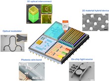
The ever-increasing demand for data capacity and information processing speed is driving the development of new techniques to break the performance limitations of current electronic-based data processing systems. Photonic integrated circuits (PICs) have been promising candidates for next-generation chip technology, featuring broad bandwidth, low power consumption, and ultrafast data processing speed. Recent advances in three-dimensional (3D) PIC fabrication and integration of two-dimensional (2D) materials with unique structures and distinctive properties have accelerated PIC development, yielding new possibilities for device realization with outstanding performance and new features. Advanced nanofabrication techniques are fundamentally important for device realization, among which laser nanofabrication, exhibiting one-step and maskless writing capability, has been widely used to fabricate 2D/3D PICs. Although there are several reviews about the fabrication of 2D or 3D PICs, none of them touched on the potential of integrating 2D materials with 3D PICs, which opens new avenues for integration and functionalities and will be substantially important for future development. This review provides a comprehensive overview of laser nanofabrication techniques in multidimensional structure manufacturing for PIC applications. Building on the recent advancements in 3D PIC fabrication and 2D-material-based functional devices, we highlight the potential of integrating 2D materials with 3D PICs. This integration paves the way for creating multidimensional structures with unprecedented optical properties and functionalities, unlocking opportunities that have yet to be explored. By highlighting these possibilities, this review aims to foster new insights and inspire novel directions in the field of PICs.
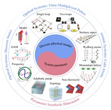
The concept of synthetic dimensions has emerged as a powerful framework in photonics and atomic physics, enabling the exploration of high-dimensional physics beyond conventional spatial constraints. Originally developed for quantum simulations in high dimensions, synthetic dimensions have since demonstrated advantages in designing novel Hamiltonians and manipulating quantum or optical states for exploring topological physics, and for applications in computing and information processing. Here, we provide a comprehensive overview of progress in synthetic dimensions across photonic, atomic, and other physical platforms over the past decade. We showcase different approaches used to construct synthetic dimensions and highlight key physical phenomena enabled by the advantage of such a framework. By offering a unified perspective on developments in this field, we aim to provide insights into how synthetic dimensions can bridge fundamental physics and applied technologies, fostering interdisciplinary engagement in quantum simulation, atomic and photonic engineering, and information processing.


