


Please enter the answer below before you can view the full text.
7+3=
Non-Hermitian physics, which studies systems with nonconservative interactions with the environment, has attracted growing interest. Unique phenomena such as enhanced sensing, the non-Hermitian skin effect, and novel topological behaviors have been extensively explored. Photonic systems serve as ideal platforms to investigate these effects because of inherent decoherence and loss of photons. Non-Hermitian photonics not only reveals intriguing physical effects but also offers new avenues for manipulating light and its associated information, enabling device-level applications. This review summarizes recent progress in non-Hermitian photonic systems. We begin by introducing key concepts and theorems, including the connection between master equations and non-Hermitian Hamiltonians, pseudo-Hermiticity, parity-time symmetry, conserved quantities, exceptional points, and biorthogonal theory. Based on this foundation, we discuss how various platforms—including bulk optics, waveguides, optical cavities, fibers, synthetic dimensions, and metamaterials—simulate non-Hermitian systems. Particular focus is given to the construction of effective non-Hermitian Hamiltonians and operators. We introduce the non-Bloch band theory through a photonic quantum walk platform, highlighting the roles of non-Hermitian topology under complex spectra, which may stimulate advances in both fundamental research and practical applications. Finally, we review unique phenomena and potential applications in sensing, chiral state transfer, quantum algorithms, and other emerging non-Hermitian photonic devices.
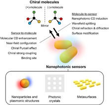
Nanophotonic chiral sensing enables the characterization of the optical activity of chiral molecules, even at ultralow concentrations, whereas conventional chiroptical spectroscopy is limited to bulk measurements requiring high concentrations. This review provides a comprehensive overview of nanophotonic chiral sensing, covering fundamental principles to practical experimental considerations. We first introduce the theoretical framework of chiral light-matter interactions, including the electromagnetic description of chiral molecules and the chiral structures of light. Discussion on the chiral structure of light encompasses spin angular momentum, optical helicity, optical chirality, and zilches. We then review various chiral sensing mechanisms, such as single-molecule circular dichroism enhancement, nanophotonically induced circular dichroism in sensor-molecule complexes, chiral spectral shifts, molecule-nanostructure Coulomb interactions, and the chiral Purcell effect, along with their experimental implementations. We also present guidance on chiroptical spectroscopy instrumentation, covering both conventional and emerging techniques. Finally, we provide our perspectives on future research directions in nanophotonic chiral sensing. We hope that this review will inspire further advancements in precise chiral sensing beyond current detection limits.
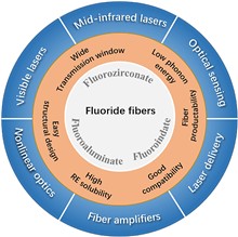
The mid-infrared (mid-IR) spectral region (2–25 µm) holds immense promise for applications in molecular spectroscopy, environmental sensing, biomedical diagnostics, and defense technologies. Among various enabling platforms, fluoride glass fibers stand out due to their broad transmission window, low phonon energy, and excellent rare-earth ion solubility, making them ideal candidates for high-efficiency mid-IR photonic systems. This review comprehensively examines the materials science, fabrication strategies, and laser applications of mid-IR fluoride fibers. We critically examine the structural and optical properties of leading glass systems—fluozirconate, fluoroaluminate, and fluoroindate—highlighting their roles in fiber design and mid-IR luminescence. State-of-the-art fabrication methods, including built-in casting, rod-in-tube, extrusion, and crucible-based fiber drawing, are analyzed in detail alongside the latest commercial fiber developments. Particular emphasis is placed on rare-earth-doped fluoride fiber lasers and supercontinuum sources, covering their physical mechanisms, system architectures, and emerging application scenarios. Finally, the current challenges in glass stability, fabrication scalability, and moisture resistance are discussed, and future research directions are proposed to advance fluoride fibers toward practical mid-IR photonic integration. This review aims to provide insights into the multidisciplinary progress driving the next generation of mid-IR fiber technologies.
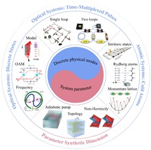
The concept of synthetic dimensions has emerged as a powerful framework in photonics and atomic physics, enabling the exploration of high-dimensional physics beyond conventional spatial constraints. Originally developed for quantum simulations in high dimensions, synthetic dimensions have since demonstrated advantages in designing novel Hamiltonians and manipulating quantum or optical states for exploring topological physics, and for applications in computing and information processing. Here, we provide a comprehensive overview of progress in synthetic dimensions across photonic, atomic, and other physical platforms over the past decade. We showcase different approaches used to construct synthetic dimensions and highlight key physical phenomena enabled by the advantage of such a framework. By offering a unified perspective on developments in this field, we aim to provide insights into how synthetic dimensions can bridge fundamental physics and applied technologies, fostering interdisciplinary engagement in quantum simulation, atomic and photonic engineering, and information processing.
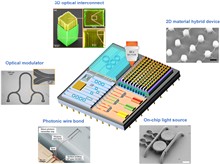
The ever-increasing demand for data capacity and information processing speed is driving the development of new techniques to break the performance limitations of current electronic-based data processing systems. Photonic integrated circuits (PICs) have been promising candidates for next-generation chip technology, featuring broad bandwidth, low power consumption, and ultrafast data processing speed. Recent advances in three-dimensional (3D) PIC fabrication and integration of two-dimensional (2D) materials with unique structures and distinctive properties have accelerated PIC development, yielding new possibilities for device realization with outstanding performance and new features. Advanced nanofabrication techniques are fundamentally important for device realization, among which laser nanofabrication, exhibiting one-step and maskless writing capability, has been widely used to fabricate 2D/3D PICs. Although there are several reviews about the fabrication of 2D or 3D PICs, none of them touched on the potential of integrating 2D materials with 3D PICs, which opens new avenues for integration and functionalities and will be substantially important for future development. This review provides a comprehensive overview of laser nanofabrication techniques in multidimensional structure manufacturing for PIC applications. Building on the recent advancements in 3D PIC fabrication and 2D-material-based functional devices, we highlight the potential of integrating 2D materials with 3D PICs. This integration paves the way for creating multidimensional structures with unprecedented optical properties and functionalities, unlocking opportunities that have yet to be explored. By highlighting these possibilities, this review aims to foster new insights and inspire novel directions in the field of PICs.
Surface plasmons are collective excitations of conduction electrons situated at the metal-dielectric interface, resulting in markedly enhanced light–matter interactions. The high local field intensity has enabled a wide range of novel physical phenomena and innovative applications. However, the small mode volume and the femtosecond dynamics necessitate rigorous experimental conditions for complete characterizations. The demand for subwavelength resolution has outpaced the capabilities of conventional methods, prompting the development of novel characterization instruments. These instruments utilize two categories of probes with exceptional resolution: nanoscale tips and electron beams. The former has led to the emergence of scanning near-field optical microscopies, while the latter has resulted in electron nanoscopies. These technologies offer ultrahigh spatiotemporal resolutions in the multi-dimensional characterization of surface plasmons. Although advanced characterization technologies have promoted multi-dimensional manipulations of surface plasmons, quantum detection is still a challenge for them. This review article provides a comprehensive overview of the recent advances in plasmonics from the perspectives of near-field optics and electron nanoscopy. It introduces the latest characterization technologies and the manipulation of surface plasmons, including their spatial distribution, energy, momentum, and polarization. Additionally, the article describes advances and challenges in quantum plasmonics and the upgrade of characterization as a potential technical solution.
The current state of traditional optoelectronic imaging technology is constrained by the inherent limitations of its hardware. These limitations pose significant challenges in acquiring higher-dimensional information and reconstructing accurate images, particularly in applications such as scattering imaging, super-resolution, and complex scene reconstruction. However, the rapid development and widespread adoption of deep learning are reshaping the field of optical imaging through computational imaging technology. Data-driven computational imaging has ushered in a paradigm shift by leveraging the nonlinear expression and feature learning capabilities of neural networks. This approach transcends the limitations of conventional physical models, enabling the adaptive extraction of critical features directly from data. As a result, computational imaging overcomes the traditional “what you see is what you get” paradigm, paving the way for more compact optical system designs, broader information acquisition, and improved image reconstruction accuracy. These advancements have significantly enhanced the interpretation of high-dimensional light-field information and the processing of complex images. This review presents a comprehensive analysis of the integration of deep learning and computational imaging, emphasizing its transformative potential in three core areas: computational optical system design, high-dimensional information interpretation, and image enhancement and processing. Additionally, this review addresses the challenges and future directions of this cutting-edge technology, providing novel insights into interdisciplinary imaging research.
Loss is usually considered a problem for photonics, which can seriously deteriorate the performance of most optical devices, and thus has to be suppressed. However, in non-Hermitian passive optical systems without gain, when both eigenvalues and eigenvectors coalesce to form exceptional points (EPs), the addition of loss may, counterintuitively, bring unique advantages, such as improved noise resistance and more stable operation. In this review, we first briefly introduce the underlying mechanisms leading to passive EPs and then examine several implementations based on different electromagnetic structures, including cavities, waveguides, and metasurfaces. We highlight the introduction of losses in each case and discuss their benefits. Finally, we also provide our thoughts on the current limits for those passive realizations as well as potential future projects.
Among super-resolution microscopy techniques, structured illumination microscopy (SIM) shows great advances in low phototoxicity, high speed, and excellent performance in long-term dynamic observation, making it especially suitable for live-cell imaging. This review delves into the principles, instrumentation, and applications of SIM, highlighting its capabilities in achieving high spatiotemporal resolution. Two types of structured illumination mechanics are employed: (1) stripe-based SIM, where the illumination stripes are formed through interference or projection, with extended resolution achieved through Fourier-domain extension; (2) point-scanning-based SIM, where illumination patterns are generated through the projection of the focal point or focal array, with extended resolution achieved through photon reassignment. We discuss the evolution of SIM from mechanical to high-speed photoelectric devices, such as spatial light modulators, digital micromirror devices, galvanometers, etc., which significantly enhance imaging speed, resolution, and modulation flexibility. The review also explores SIM’s applications in biological research, particularly in live-cell imaging and cellular interaction studies, providing insights into disease mechanisms and cellular functions. We conclude by outlining the future directions of SIM in life sciences. With the advancement of imaging techniques and reconstruction algorithms, SIM is poised to bring revolutionary impacts to frontier research fields, offering new avenues for exploring the intricacies of cellular biology.
Integrated microcombs bring a parallel and coherent optical frequency comb to compact chip-scale devices. They offer promising prospects for mass-produced comb sources in a compact, power-efficient, and robust manner, benefiting many basic research and practical applications. In the past two decades, they have been utilized in many traditional fields, such as high-capacity parallel communication, optical frequency synthesis, frequency metrology, precision spectroscopy, and emerging fields like distance ranging, optical computing, microwave photonics, and molecule detection. In this review, we briefly introduce microcombs, including their physical model, formation dynamics, generation methods, materials and fabrications, design principles, and advanced applications. We also systematically summarize the field of integrated optical combs and evaluate the remaining challenges and prospects in each aspect.
Spatiotemporal optical wavepackets refer to light fields with sophisticated structures in both space and time. The ability to produce such spatiotemporally structured optical wavepackets on demand attracted rapidly increasing interest as it may unravel a variety of fundamental physical effects and applications. Traditionally, pulsed laser fields are treated as spatiotemporally separable waveform solutions to Maxwell’s equations. Recently, more generalized spatiotemporally non-separable solutions have gained attention due to their remarkable properties. This review aims to provide essential insights into sculpting light in the space–time domain to create customized spatiotemporal structures and highlights the recent advances in the generation, manipulation, and characterization of increasingly complex spatiotemporal wavepackets. These spatiotemporally non-separable light fields with diverse geometric and topological structures exhibit unique physical properties during propagation, focusing, and light–matter interactions. Various novel results and their broad potential applications as well as an outlook for future trends and challenges in this field are presented.
Optical metasurfaces have emerged as a groundbreaking technology in photonics, offering unparalleled control over light–matter interactions at the subwavelength scale with ultrathin surface nanostructures and thereby giving birth to flat optics. While most reported optical metasurfaces are static, featuring well-defined optical responses determined by their compositions and configurations set during fabrication, dynamic optical metasurfaces with reconfigurable functionalities by applying thermal, electrical, or optical stimuli have become increasingly more in demand and moved to the forefront of research and development. Among various types of dynamically controlled metasurfaces, electrically tunable optical metasurfaces have shown great promise due to their fast response time, low power consumption, and compatibility with existing electronic control systems, offering unique possibilities for dynamic tunability of light–matter interactions via electrical modulation. Here we provide a comprehensive overview of the state-of-the-art design methodologies and technologies explored in this rapidly evolving field. Our work delves into the fundamental principles of electrical modulation, various materials and mechanisms enabling tunability, and representative applications for active light-field manipulation, including optical amplitude and phase modulators, tunable polarization optics and wavelength filters, and dynamic wave-shaping optics, including holograms and displays. The review terminates with our perspectives on the future development of electrically triggered optical metasurfaces.
Photoacoustic computed tomography (PACT) is a rapidly developing biomedical imaging modality and has attracted substantial attention in recent years. Image reconstruction from photoacoustic projections plays a critical role in image formation in PACT. Here we review six major classes of image reconstruction approaches developed in the past three decades, including delay and sum, filtered back projection, series expansion, time reversal, iterative reconstruction, and deep-learning-based reconstruction. The principal ideas and implementations of the algorithms are summarized, and their reconstruction performances under different imaging scenarios are compared. Major challenges, future directions, and perspectives for the development of image reconstruction algorithms in PACT are also discussed. This review provides a self-contained reference guide for beginners and specialists in the photoacoustic community, to facilitate the development and application of novel photoacoustic image reconstruction algorithms.
Structured light, also known as tailored light, shaped light, sculpted light, or custom light, refers to a series of special light beams with spatially variant amplitudes and phases, polarization distributions, or more general spatiotemporal profiles. In the past decades, structured light featuring distinct properties and unique spatial or spatiotemporal structures has grown into a significant research field and given rise to many developments from fundamentals to applications. Very recently, integrated structured light manipulation has become an important trend in the frontier of light field manipulation and attracted increasing interest as a highly promising technique for shaping structured light in an integrated, compact, and miniaturized manner. In this article, we give a comprehensive overview of recent advances in integrated structured light manipulation (generation, processing, detection, and application). After briefly introducing the basic concept and development history of structured light, we present representative works in four important aspects of integrated structured light manipulation, including multiple types of integrated structured light generation, many sorts of integrated structured light processing, diverse forms of integrated structured light detection, and various kinds of integrated structured light applications. We focus on summarizing the progress of integrated structured light manipulation from basic theories to cutting-edge technologies, to key devices, and to a wide variety of applications, from orbital angular momentum carrying light beams to more general structured light beams, from passive to active integration platforms, from micro-nano structures and metasurfaces to 2D photonic integrated circuits and 3D photonic chips, from in-plane to out-of-plane, from multiplexing to transformation, from linear to nonlinear, from classical to quantum, from optical communications to optical holography, imaging, microscopy, trapping, tweezers, metrology, etc. Finally, we also discuss in detail the future trends, opportunities, challenges, and solutions, and give a vision for integrated structured light manipulation.
Metasurfaces, composed of two-dimensional nanostructures, exhibit remarkable capabilities in shaping wavefronts, encompassing phase, amplitude, and polarization. This unique proficiency heralds a transformative paradigm shift in the domain of next-generation optics and photonics, culminating in the development of flat and ultrathin optical devices. Particularly noteworthy is the all-dielectric-based metasurface, leveraging materials such as titanium dioxide, silicon, gallium arsenide, and silicon nitride, which finds extensive application in the design and implementation of high-performance optical devices, owing to its notable advantages, including a high refractive index, low ohmic loss, and cost-effectiveness. Furthermore, the remarkable growth in nanofabrication technologies allows for the exploration of new methods in metasurface fabrication, especially through wafer-scale nanofabrication technologies, thereby facilitating the realization of commercial applications for metasurfaces. This review provides a comprehensive overview of the latest advancements in state-of-the-art fabrication technologies in dielectric metasurface areas. These technologies, including standard nanolithography [e.g., electron beam lithography (EBL) and focused ion beam (FIB) lithography], advanced nanolithography (e.g., grayscale and scanning probe lithography), and large-scale nanolithography [e.g., nanoimprint and deep ultraviolet (DUV) lithography], are utilized to fabricate high-resolution, high-aspect-ratio, flexible, multilayer, slanted, and wafer-scale all-dielectric metasurfaces with intricate nanostructures. Ultimately, we conclude with a perspective on current cutting-edge nanofabrication technologies.
Structural coloration generates colors by the interaction between incident light and micro- or nano-scale structures. It has received tremendous interest for decades, due to advantages including robustness against bleaching and environmentally friendly properties (compared with conventional pigments and dyes). As a versatile coloration strategy, the tuning of structural colors based on micro- and nanoscale photonic structures has been extensively explored and can enable a broad range of applications including displays, anti-counterfeiting, and coating. However, scholarly research on structural colors has had limited impact on commercial products because of their disadvantages in cost, scalability, and fabrication. In this review, we analyze the key challenges and opportunities in the development of structural colors. We first summarize the fundamental mechanisms and design strategies for structural colors while reviewing the recent progress in realizing dynamic structural coloration. The promising potential applications including optical information processing and displays are also discussed while elucidating the most prominent challenges that prevent them from translating into technologies on the market. Finally, we address the new opportunities that are underexplored by the structural coloration community but can be achieved through multidisciplinary research within the emerging research areas.
An optical micro/nanofiber (MNF) is a quasi-one-dimensional free-standing optical waveguide with a diameter close to or less than the vacuum wavelength of light. Combining the tiny geometry with high-refractive-index contrast between the core and the surrounding, the MNF exhibits favorable optical properties such as tight optical confinement, strong evanescent field, and large-diameter-dependent waveguide dispersion. Meanwhile, as a quasi-one-dimensional structure with extraordinarily high geometric and structural uniformity, the MNF also has low optical loss and high mechanical strength, making it favorable for manipulating light on the micro/nanoscale with high flexibility. Over the past two decades, optical MNFs, typically being operated in single mode, have been emerging as a miniaturized fiber-optic platform for both scientific research and technological applications. In this paper, we aim to provide a comprehensive overview of the representative advances in optical MNFs in recent years. Starting from the basic structures and fabrication techniques of the optical MNFs, we highlight linear and nonlinear optical and mechanical properties of the MNFs. Then, we introduce typical applications of optical MNFs from near-field optics, passive optical components, optical sensors, and optomechanics to fiber lasers and atom optics. Finally, we give a brief summary of the current status of MNF optics and technology, and provide an outlook into future challenges and opportunities.
Optical bound states in the continuum (BICs) have recently stimulated a research boom, accompanied by demonstrations of abundant exotic phenomena and applications. With ultrahigh quality (Q) factors, optical BICs have powerful abilities to trap light in optical structures from the continuum of propagation waves in free space. Besides the high Q factors enabled by the confined properties, many hidden topological characteristics were discovered in optical BICs. Especially in periodic structures with well-defined wave vectors, optical BICs were discovered to carry topological charges in momentum space, underlying many unique physical properties. Both high Q factors and topological vortex configurations in momentum space enabled by BICs bring new degrees of freedom to modulate light. BICs have enabled many novel discoveries in light–matter interactions and spin–orbit interactions of light, and BIC applications in lasing and sensing have also been well explored with many advantages. In this paper, we review recent developments of optical BICs in periodic structures, including the physical mechanisms of BICs, explored effects enabled by BICs, and applications of BICs. In the outlook part, we provide a perspective on future developments for BICs.
Diffractive optical elements (DOEs) are intricately designed devices with the purpose of manipulating light fields by precisely modifying their wavefronts. The concept of DOEs has its origins dating back to 1948 when D. Gabor first introduced holography. Subsequently, researchers introduced binary optical elements (BOEs), including computer-generated holograms (CGHs), as a distinct category within the realm of DOEs. This was the first revolution in optical devices. The next major breakthrough in light field manipulation occurred during the early 21st century, marked by the advent of metamaterials and metasurfaces. Metasurfaces are particularly appealing due to their ultra-thin, ultra-compact properties and their capacity to exert precise control over virtually every aspect of light fields, including amplitude, phase, polarization, wavelength/frequency, angular momentum, etc. The advancement of light field manipulation with micro/nano-structures has also enabled various applications in fields such as information acquisition, transmission, storage, processing, and display. In this review, we cover the fundamental science, cutting-edge technologies, and wide-ranging applications associated with micro/nano-scale optical devices for regulating light fields. We also delve into the prevailing challenges in the pursuit of developing viable technology for real-world applications. Furthermore, we offer insights into potential future research trends and directions within the realm of light field manipulation.
Free-electron light sources feature extraordinary luminosity, directionality, and coherence, which has enabled significant scientific progress in fields including physics, chemistry, and biology. The next generation of light sources has aimed at compact radiation sources driven by free electrons, with the advantages of reduction in both space and cost. With the rapid development of ultra-intense and ultrashort lasers, great effort has been devoted to the quest for compact free-electron lasers (FELs). This review focuses on the current efforts and advancements in the development of compact FELs, with a particular emphasis on two notable paths: the development of compact accelerators and the construction of micro undulators based on innovative materials/structures or optical modulation of electrons. In addition, the physical essence of inverse Compton scattering is discussed, which offers remarkable capability to develop an optical undulator with a spatial period that matches the optical wavelength. Recent scientific developments and future directions for miniaturized and integrated free-electron coherent light sources are also reviewed. In the future, the prospect of generating ultrashort electron pulses will provide fascinating means of producing superradiant radiation, promising high brilliance and coherence even on a micro scale using optical micro undulators.
Ultra-broadband, intense, coherent terahertz (THz) radiation can be generated, detected, and manipulated using laser-induced gas or liquid plasma as both the THz wave transmitter and detector, with a frequency coverage spanning across and beyond the whole “THz gap.” Such a research topic is termed “plasma-based THz wave photonics in gas and liquid phases.” In this paper, we review the most important experimental and theoretical works of the topic in the non-relativistic region with pump laser intensity below 1018 W/cm2.
Light carries energy and momentum, laying the physical foundation of optical manipulation that has facilitated advances in myriad scientific disciplines, ranging from biochemistry and robotics to quantum physics. Utilizing the momentum of light, optical tweezers have exemplified elegant light–matter interactions in which mechanical and optical momenta can be interchanged, whose effects are the most pronounced on micro and nano objects in fluid suspensions. In solid domains, the same momentum transfer becomes futile in the face of dramatically increased adhesion force. Effective implementation of optical manipulation should thereupon switch to the “energy” channel by involving auxiliary physical fields, which also coincides with the irresistible trend of enriching actuation mechanisms beyond sole reliance on light-momentum-based optical force. From this perspective, this review covers the developments of optical manipulation in schemes of both momentum and energy transfer, and we have correspondingly selected representative techniques to present. Theoretical analyses are provided at the beginning of this review followed by experimental embodiments, with special emphasis on the contrast between mechanisms and the practical realization of optical manipulation in fluid and solid domains.
Advancements in micro/nanofabrication have enabled the realization of practical micro/nanoscale photonic devices such as absorbers, solar cells, metalenses, and metaholograms. Although the performance of these photonic devices has been improved by enhancing the design flexibility of structural materials through advanced fabrication methods, achieving large-area and high-throughput fabrication of tiny structural materials remains a challenge. In this aspect, various technologies have been investigated for realizing the mass production of practical devices consisting of micro/nanostructural materials. This review describes the recent advancements in soft lithography, colloidal self-assembly, and block copolymer self-assembly, which are promising methods suitable for commercialization of photonic applications. In addition, we introduce low-cost and large-scale techniques realizing micro/nano devices with specific examples such as display technology and sensors. The inferences presented in this review are expected to function as a guide for promising methods of accelerating the mass production of various sub-wavelength-scale photonic devices.
Low symmetry 2D materials with intrinsic in-plane anisotropic optical properties and high tunability provide a promising platform to explore and manipulate light–matter interactions. To date, dozens of in-plane anisotropic 2D materials with diverse band structures have been discovered. They exhibit rich optical properties, indicating great potential for novel applications in optics, photonics, and optoelectronics. In this paper, we thoroughly review the anisotropic optical properties and polaritons in many kinds of low symmetry 2D materials, aiming to elicit more research interest in this field. First, the optical properties of anisotropic 2D semiconductors, including interband absorption, photoluminescence, excitons, and band structure engineering for tuning optical responses, are introduced. Then fundamentals and advances in experiments of hyperbolic polaritons in anisotropic 2D materials, including phonon, plasmon, and exciton polaritons, are discussed. Finally, a perspective on promising research directions is given.
Surface plasmons (SPs) are electromagnetic surface waves that propagate at the interface between a conductor and a dielectric. Due to their unique ability to concentrate light on two-dimensional platforms and produce very high local-field intensity, SPs have rapidly fueled a variety of fundamental advances and practical applications. In parallel, the development of metamaterials and metasurfaces has rapidly revolutionized the design concepts of traditional optical devices, fostering the exciting field of meta-optics. This review focuses on recent progress of meta-optics inspired SP devices, which are implemented by the careful design of subwavelength structures and the arrangement of their spatial distributions. Devices of general interest, including coupling devices, on-chip tailoring devices, and decoupling devices, as well as nascent SP applications empowered by sophisticated usage of meta-optics, are introduced and discussed.
The refractive-lens technique has been well developed over a long period of evolution, offering powerful imaging functionalities, such as microscopes, telescopes, and spectroscopes. Nevertheless, the ever-growing requirements continue to urge further enhanced imaging capabilities and upgraded devices that are more compact for convenience. Metamaterial as a fascinating concept has inspired unprecedented new explorations in physics, material science, and optics, not only in fundamental researches but also novel applications. Along with the imaging topic, this paper reviews the progress of the flat lens as an important branch of metamaterials, covering the early superlens with super-diffraction capability and current hot topics of metalenses including a paralleled strategy of multilevel diffractive lenses. Numerous efforts and approaches have been dedicated to areas ranging from the new fascinating physics to feasible applications. This review provides a clear picture of the flat-lens evolution from the perspective of metamaterial design, elucidating the relation and comparison between a superlens and metalens, and addressing derivative designs. Finally, application scenarios that favor the ultrathin lens technique are emphasized with respect to possible revolutionary imaging devices, followed by conclusive remarks and prospects.
Epitaxial quantum dots formed by III–V compound semiconductors are excellent sources of non-classical photons, creating single photons and entangled multi-photon states on demand. Their semiconductor nature allows for a straightforward combination with mature integrated photonic technologies, leading to novel functional devices at the single-photon level. Integrating a quantum dot into a carefully engineered photonic cavity enables control of the radiative decay rate using the Purcell effect and the realization of photon–photon nonlinear gates. In this review, we introduce the basis of epitaxial quantum dots and discuss their applications as non-classical light sources. We highlight two interfaces—one between flying photons and the quantum-dot dipole, and the other between the photons and the spin. We summarize the recent development of integrated photonics and reconfigurable devices that have been combined with quantum dots or are suitable for hybrid integration. Finally, we provide an outlook of employing quantum-dot platforms for practical applications in large-scale quantum computation and the quantum Internet.
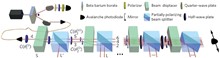
The four-wave mixing process in atomic ensembles has many important applications in quantum information. We review recent progress on the generation of optical quantum states from the four-wave mixing process in hot atomic ensembles, including the production of two-beam, multi-beam, and multiplexed quantum correlated or entangled states. We also review the applications of these optical quantum states in implementing quantum information protocols, constructing SU(1,1) quantum interferometers, and realizing quantum plasmonic sensing. These applications indicate that the four-wave mixing process in hot atomic ensembles is a promising platform for quantum information processing, especially for implementing all-optical quantum information protocols, constructing SU(1,1) interferometers, and realizing quantum sensing.
Recent interest in developing fast spintronic devices and laser-controllable magnetic solids has sparked tremendous experimental and theoretical efforts to understand and manipulate ultrafast dynamics in materials. Studies of spin dynamics in the terahertz (THz) frequency range are particularly important for elucidating microscopic pathways toward novel device functionalities. Here, we review THz phenomena related to spin dynamics in rare-earth orthoferrites, a class of materials promising for antiferromagnetic spintronics. We expand this topic into a description of four key elements. (1) We start by describing THz spectroscopy of spin excitations for probing magnetic phase transitions in thermal equilibrium. While acoustic magnons are useful indicators of spin reorientation transitions, electromagnons that arise from dynamic magnetoelectric couplings serve as a signature of inversion-symmetry-breaking phases at low temperatures. (2) We then review the strong laser driving scenario, where the system is excited far from equilibrium and thereby subject to modifications to the free-energy landscape. Microscopic pathways for ultrafast laser manipulation of magnetic order are discussed. (3) Furthermore, we review a variety of protocols to manipulate coherent THz magnons in time and space, which are useful capabilities for antiferromagnetic spintronic applications. (4) Finally, new insights into the connection between dynamic magnetic coupling in condensed matter and the Dicke superradiant phase transition in quantum optics are provided. By presenting a review on an array of THz spin phenomena occurring in a single class of materials, we hope to trigger interdisciplinary efforts that actively seek connections between subfields of spintronics, which will facilitate the invention of new protocols of active spin control and quantum phase engineering.
The quest for realizing novel fundamental physical effects and practical applications in ambient conditions has led to tremendous interest in microcavity exciton polaritons working in the strong coupling regime at room temperature. In the past few decades, a wide range of novel semiconductor systems supporting robust exciton polaritons have emerged, which has led to the realization of various fascinating phenomena and practical applications. This paper aims to review recent theoretical and experimental developments of exciton polaritons operating at room temperature, and includes a comprehensive theoretical background, descriptions of intriguing phenomena observed in various physical systems, as well as accounts of optoelectronic applications. Specifically, an in-depth review of physical systems achieving room temperature exciton polaritons will be presented, including the early development of ZnO and GaN microcavities and other emerging systems such as organics, halide perovskite semiconductors, carbon nanotubes, and transition metal dichalcogenides. Finally, a perspective of outlooking future developments will be elaborated.
The geometric phase concept has profound implications in many branches of physics, from condensed matter physics to quantum systems. Although geometric phase has a long research history, novel theories, devices, and applications are constantly emerging with developments going down to the subwavelength scale. Specifically, as one of the main approaches to implement gradient phase modulation along a thin interface, geometric phase metasurfaces composed of spatially rotated subwavelength artificial structures have been utilized to construct various thin and planar meta-devices. In this paper, we first give a simple overview of the development of geometric phase in optics. Then, we focus on recent advances in continuously shaped geometric phase metasurfaces, geometric–dynamic composite phase metasurfaces, and nonlinear and high-order linear Pancharatnam–Berry phase metasurfaces. Finally, conclusions and outlooks for future developments are presented.
Originally a pure mathematical concept, topology has been vigorously developed in various physical systems in recent years, and underlies many interesting phenomena such as the quantum Hall effect and quantum spin Hall effect. Its widespread influence in physics led the award of the 2016 Nobel Prize in Physics to this field. Topological photonics further expands the research field of topology to classical wave systems and holds promise for novel devices and applications, e.g., topological quantum computation and topological lasers. Here, we review recent developments in topological photonics but focus mainly on their realizations based on metamaterials. Through artificially designed resonant units, metamaterials provide vast degrees of freedom for realizing various topological states, e.g., the Weyl point, nodal line, Dirac point, topological insulator, and even the Yang monopole and Weyl surface in higher-dimensional synthetic spaces, wherein each specific topological nontrivial state endows novel metamaterial responses that originate from the feature of some high-energy physics.
Metamaterials and metasurfaces have inspired worldwide interest in the recent two decades due to their extraordinary performance in controlling material parameters and electromagnetic properties. However, most studies on metamaterials and metasurfaces are focused on manipulations of electromagnetic fields and waves, because of their analog natures. The concepts of digital coding and programmable metasurfaces proposed in 2014 have opened a new perspective to characterize and design metasurfaces in a digital way, and made it possible to control electromagnetic fields/waves and process digital information simultaneously, yielding the birth of a new direction of information metasurfaces. On the other hand, artificial intelligence (AI) has become more important in automatic designs of metasurfaces. In this review paper, we first show the intrinsic natures and advantages of information metasurfaces, including information operations, programmable and real-time control capabilities, and space–time-coding strategies. Then we introduce the recent advances in designing metasurfaces using AI technologies, and particularly discuss the close combinations of information metasurfaces and AI to generate intelligent metasurfaces. We present self-adaptively smart metasurfaces, AI-based intelligent imagers, microwave cameras, and programmable AI machines based on optical neural networks. Finally, we indicate the challenges, applications, and future directions of information and intelligent metasurfaces.