


Please enter the answer below before you can view the full text.
3-2=
The polarization properties of light are widely applied in imaging, communications, materials analysis, and life sciences. Various methods have been developed that can measure the polarization information of a target. However, conventional polarization detection systems are often bulky and complex, limiting their potential for broader applications. To address the challenges of miniaturization, integrated polarization detectors have been extensively explored in recent years, achieving significant advancements in performance and functionality. In this review, we focus mainly on integrated polarization detectors with innovative features, including infinitely high polarization discrimination, ultrahigh sensitivity to polarization state change, full Stokes parameters measurement, and simultaneous perception of polarization and other key properties of light. Lastly, we discuss the opportunities and challenges for the future development of integrated polarization photodetectors.
To enhance the net photoelectric conversion efficiency of quantum well infrared photodetectors, this study investigates the matching conditions between radiative dissipation and coupling strength in devices operating in the strong light-matter coupling regime. A critical coupling model distinct from the conventional intrinsic and radiative dissipation matching is proposed. Through an analytical model, the contributions of intrinsic thermal dissipation and coupling strength to the critical conditions are quantified. The results indicate that, with optimized matching parameters, the net photoelectric absorption efficiency, excluding thermal dissipation, can exceed 95%. Moreover, under the synergistic regulation of the strong coupling mechanism and critical coupling conditions, the photodetection response can be enhanced by up to 160%. This work highlights the importance of optimizing dissipation and coupling parameters under strong coupling conditions, providing theoretical and design guidance for improving photoelectric conversion efficiency and enhancing the performance of quantum well infrared photodetectors.
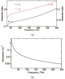
Electro-Optic Sampling (EOS) detection technique has been widely used in terahertz science and technology, and it also can measure the field time waveform of the few-cycle laser pulse. Its frequency response and band limitation are determined directly by the electro-optic crystal and duration of the probe laser pulse. Here, we investigate the performance of the EOS with thin GaSe crystal in the measurement of the mid-infrared few-cycle laser pulse. The shift of the central frequency and change of the bandwidth induced by the EOS detection are calculated, and then the pulse distortions induced in this detection process are discussed. It is found that this technique produces a red-shift of the central frequency and narrowing of the bandwidth. These changings decrease when the laser wavelength increases from 2 μm to 10 μm. This work can help to estimate the performance of the EOS detection technique in the mid-infrared band and offer a reference for the related experiment as well.
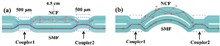
A novel near-infrared all-fiber mode monitor based on a mini-two-path Mach-Zehnder interferometer (MTP-MZI) is proposed. The MTP-MZI mode monitor is created by fusing a section of (no-core fiber ,NCF) and a (single-mode fiber ,SMF) together with an optical fiber fusion splicer, establishing two distinct centimeter-level optical transmission paths. Since the high-order modes in NCF transmit near-infrared light more sensitively to curvature-induced energy leakage than the fundamental mode in SMF, the near-infrared high-order mode light leaks out of NCF when the curvature changes, causing the MTP-MZI transmission spectrum to change. By analyzing the relationship between the curvature, transmission spectrum, and spatial frequency spectrum, the modes involved in the interference can be studied, thereby revealing the mode transmission characteristics of near-infrared light in optical fibers. In the verification experiments, higher-order modes were excited by inserting a novel hollow-core fiber (HCF) into the MTP-MZI. When the curvature of the MTP-MZI changes, the near-infrared light high-order mode introduced into the device leaks out, causing the transmission spectrum to return to its original state before bending and before the HCF was spliced. The experimental results demonstrate that the MTP-MZI mode monitor can monitor the fiber modes introduced from the external environment, providing both theoretical and experimental foundations for near-infrared all-fiber mode monitoring in optical information systems.
Unmanned Aerial Vehicles(UAVs) have a wide range of applications in agriculture, logistics, rescue and disaster relief because of their compactness, lightness and flexibility. However, if they are used improperly or mismanaged, they may not only cause personal privacy leakage and property loss, but also pose a threat to public safety and even military security. Therefore, real-time and accurate detection and warning of UAVs in the airspace play an important role. In this regard, a multi-channel interactive attention mechanism and edge contour enhancement (MCIAECE) method for infrared UAV detection is proposed. Firstly, the shallow and deep features of the infrared image are extracted by a dual-channel consisting of a multi-channel interactive attention mechanism module and an edge contour enhancement module, after which the attention mechanism enhances the target features while the edge contour enhancement obtains more detailed information. Then the extracted features of each layer are fused and enhanced using the multilevel feature fusion module to obtain the detection results. The experimental results show that better results can be achieved with the MCIAECE method on all three datasets. Among them, the best results are obtained on the NUDT-SIRST infrared dataset, with the detection probability and intersection over union of 98.83% and 85.11% respectively, which increased by 1.95% and 6.88% compared to the baseline network,and the effect is significant in the edge contour restoration of the target compared with other methods.
This paper investigates the punch-through characteristics of separate absorption, charge and multiplication avalanche photodetector (SACM APD). By analyzing the device's spectral response, capacitance characteristics, and I-V characteristics at various operating temperatures, and combining these with simulated internal electric field and energy band distributions from the SILVACO platform, we analyzed examined the performance of the SACM APD before and after punch-through and established a corresponding mathematical model. Through structural and process parameter optimization for silicon-based SACM APD devices, simulations revealed that when the ion implantation energy of the field-control layer was 580 keV, the optimized device exhibited a punch-through threshold voltage of -30 V and a capacitance reduction to one-third of the pre-punch-through value. Subsequently, a silicon SACM APD device was fabricated using the complementary metal-oxide-semiconductor (CMOS) process. Measurements confirmed a punch-through threshold voltage of -30 V, a 2.18-fold increase in photocurrent at 808 nm (punch-through), a redshift of the peak responsivity wavelength from 590 nm (pre-punch-through) to 820 nm (post-punch-through), and an elevation of the peak responsivity from 0.171 A/W@590 nm to 0.377 A/W@820 nm. The capacitance was also reduced to one-third of the pre-punch-through value at 1 MHz.
Lasers with wavelengths around 2 μm are located in the atmospheric transmission window and at the strong absorption peak of water, and have important applications in medicine, LIDAR, material processing, and pump sources for mid-infrared lasers. The thulium-doped fiber laser (TDFL) stands out as a critical light source capable of delivering high power outputs at this wavelength. In this paper, to address the problems of relaxation oscillation and inter-modal four-wave mixing in a quasi-continuous wave (QCW) TDFL, the time and frequency-domain output characteristics of the laser are optimized by increasing the bias current, optimizing the length of the gain fiber, and changing the diameter of the fiber coiling, etc. The effects of different gain fiber structures on the fiber transmission modes are also investigated. The developed QCW-TDFL achieves a peak power of 894 W and an average power of 89.4 W at a central wavelength of 1 939.2 nm with a pulse width of 100 μs, a repetition frequency of 1 kHz and a duty cycle of 10%, and obtains stable and controllable pulse output waveform and spectral characteristics.
The preparation of quantum dot thin films and the accurate measurement of optical constants are particularly important for the development and application of quantum dot devices in optoelectronic fields. At present, the optical constants of MoTe2 single-crystal films prepared by mechanical exfoliation and chemical vapor deposition are relatively mature. However, the optical constants of 2H-MoTe2 quantum dot films are rarely reported.In this work, 2H-MoTe2 quantum dots were prepared by ultrasonic assisted liquid phase exfoliation, and of 2H-MoTe2 quantum dots with two sizes were acquired via adjusting the type of solvent and the order of ultrasonic process. The optical constants such as refractive index, extinction coefficient and dielectric constant of quantum dot films of two sizes were studied by B-spline model and Tauc-Lorentz model using ellipsometry. The results demonstrate that the 2H-MoTe2 quantum dots with two sizes have similar refractive index, extinction coefficient and a wider spectral absorption in the visible to near infrared band. And compared with MoTe2 bulk material, 2H-MoTe, quantom dots have a lower dielectric constant.
The sensitivity of the detector is the core technical indicator of the infrared detector. Short-wave infrared detector has low dark current and the sensitivity will be limited by the inherent read-out circuit noise of the detection system. Therefore, it is an effective way to further enhance the sensitivity by introducing internal gain into the detector. The heterogeneous phototransistor has advantages of high gain, low operating bias, and low excess noise, which provides novel approach for high-sensitive detection. This paper mainly focuses on the simulation design of InGaAs/GaAsSb type-II superlattice short-wave infrared phototransistor, and studies the dependence of the device size on the optoelectronic characteristics. The results show that a higher gain, a lower dark current, and a faster response can be achieved by a smaller base size. Based on the optimization design of size structure, a noise equivalent photon lower than 10 can be achieved, which provides a new technical approach to achieve high-sensitive heterogeneous phototransistor detector.
Colloidal quantum dots (CQDs) are affected by the quantum confinement effect, which makes their bandgap tunable. This characteristic allows these materials to cover a broader infrared spectrum, providing a cost-effective alternative to traditional infrared detector technology. Recently, thanks to the solution processing properties of quantum dots and their ability to integrate with silicon-based readout circuits on a single chip, infrared detectors based on HgTe CQDs have shown great application prospects. However, facing the challenges of vertically stacked photovoltaic devices, such as barrier layer matching and film non-uniformity, most devices integrated with readout circuits still use a planar structure, which limits the efficiency of light absorption and the effective separation and collection of photo-generated carriers. Here, by synthesizing high-quality HgTe CQDs and precisely controlling the interface quality, we have successfully fabricated a photovoltaic detector based on HgTe and ZnO QDs. At a working temperature of 80 K, this detector achieved a low dark current of 5.23×10⁻⁹ A cm-2, a high rectification ratio, and satisfactory detection sensitivity. This work paves a new way for the vertical integration of HgTe CQDs on silicon-based readout circuits, demonstrating their great potential in the field of high-performance infrared detection.
In the realm of optoelectronics, photodetectors play pivotal roles, with applications spanning from high-speed data communication to precise environmental sensing. Despite the advancements, conventional photodetectors grapple with challenges with response speed and dark current. In this study, we present a photodetector based on a lateral MoTe2 p-n junction, defined by a semi-floating ferroelectric gate. The strong ferroelectric fields and the depletion region of the p-n junction in the device are notably compact, which diminish the carrier transit time, thereby enhancing the speed of the photoelectric response. The non-volatile MoTe2 homojunction, under the influence of external gate voltage pulses, can alter the orientation of the intrinsic electric field within the junction. As a photovoltaic detector, it achieves an ultra-low dark current of 20 pA, and a fast photo response of 2 μs. The spectral response is extended to the shortwave infrared range at 1550 nm. Furthermore, a logic computing system with light/no light as binary input is designed to convert the current signal to the voltage output. This research not only underscores the versatility of 2D materials in the realm of sophisticated photodetector design but also heralds new avenues for their application in energy-efficient, high-performance optoelectronic devices.
With the development of remote sensing technology, the detection sensitivity of infrared system is increasingly required. The infrared imaging detection technology based on linear avalanche device can effectively improve the detection sensitivity in high frame frequency applications. Based on the short-wave infrared linear avalanche detector assembly of 512×512, a small-aperture and lightweight infrared imaging system is designed and its performance is tested under low reverse bias. The test results show that the increase of SNR of the imaging system based on the linear avalanche infrared detector is basically linear with the multiplication factor M under short integration time, and the SNR of the system is 3 times that of the traditional camera of the same caliber.
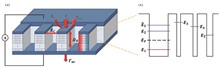
Dual-band thermal emitters with narrow bandwidths are important in various applications in the infrared field, such as in infrared sensing and infrared imaging. However, conditions for narrowband emission in different wavelengths can conflict with each other, making it difficult to achieve dual-band emitter. In this paper, a new type of lithography-free infrared dual-band thermal emitter is proposed, which consists of alternately deposited Ge and YbF3 films on Al films. The narrowband emission characteristics stem from the Tamm plasmon polaritons (TPP) that can be excited by the distributed Bragg reflector and the Al substrate under certain conditions. The geometric parameters are optimized using multi-objective particle swarm optimization. The experiment results confirm that dual-band emitter can simultaneously exhibit narrowband emitter characteristics in both mid-wave infrared (MWIR) and long-wave infrared (LWIR) regions. The proposed method can be used in the design of multi-band emitssion modulation applications, which can be applied in the fields of multi-gas sensing and multi-band infrared camouflage.
Organic semiconductor materials have shown unique advantages in the development of optoelectronic devices due to their ease of preparation, low cost, lightweight, and flexibility. In this work, we explored the application of the organic semiconductor Y6-1O single crystal in photodetection devices. Firstly, Y6-1O single crystal material was prepared on a silicon substrate using solution droplet casting method. The optical properties of Y6-1O material were characterized by polarized optical microscopy, fluorescence spectroscopy, etc., confirming its highly single crystalline performance and emission properties in the near-infrared region. Phototransistors based on Y6-1O materials with different thicknesses were then fabricated and tested. It was found that the devices exhibited good visible to near-infrared photoresponse, with the maximum photoresponse in the near-infrared region at 785 nm. The photocurrent on/off ratio reaches 102, and photoresponsivity reaches 16 mA/W. It was also found that the spectral response of the device could be regulated by gate voltage as well as the material thickness, providing important conditions for optimizing the performance of near-infrared photodetectors. This study not only demonstrates the excellent performance of organic phototransistors based on Y6-1O single crystal material in near-infrared detection but also provides new ideas and directions for the future development of infrared detectors.
In this work, we investigate the impact of the whole small recess offset on DC and RF characteristics of InP high electron mobility transistors (HEMTs). Lg = 80 nm HEMTs are fabricated with a double-recessed gate process. We focus on their DC and RF responses, including the maximum transconductance (gm_max), ON-resistance (RON), current-gain cutoff frequency (fT), and maximum oscillation frequency (fmax). The devices have almost same RON. The gm_max improves as the whole small recess moves toward the source. However, a small gate to source capacitance (Cgs) and a small drain output conductance (gds) lead to the largest fT, although the whole small gate recess moves toward the drain leads to the smaller gm_max. According to the small-signal modeling, the device with the whole small recess toward drain exhibits an excellent RF characteristics, such as fT = 372 GHz and fmax= 394 GHz. This result is achieved by paying attention to adjust resistive and capacitive parasitics, which play a key role in high-frequency response.
This paper discusses the influence of Sb/In ratio on the transport properties and crystal quality of the 200 nm InAsxSb1-x thin film. The Sb content of InAsxSb1-x thin film in all samples was verified by HRXRD of the symmetrical 004 reflections and asymmetrical 115 reflections. The calculation results show that the Sb component was 0.6 in the InAsxSb1-x thin film grown under the conditions of Sb/In ratio of 6 and As/In ratio of 3, which has the highest electron mobility (28 560 cm2/V·s) at 300 K. At the same time, the influence of V/III ratio on the transport properties and crystal quality of Al0.2In0.8Sb/InAsxSb1-x quantum well heterostructures also has been investigated. As a result, the Al0.2In0.8Sb/InAs0.4Sb0.6 quantum well heterostructure with a channel thickness of 30 nm grown under the conditions of Sb/In ratio of 6 and As/In ratio of 3 has a maximum electron mobility of 28 300 cm2/V·s and a minimum RMS roughness of 0.68 nm. Through optimizing the growth conditions, our samples have higher electron mobility and smoother surface morphology.
The master oscillator power amplifier (MOPA) laser is receiving increasing attention due to its ability to achieve high power and beam quality output. In order to improve the polarization degree of MOPA laser and reduce the efficiency loss during polarization combining, InGaAs/AlGaAs compressive single quantum well was used in the active region. The optical confinement factor of TE-mode in ridge waveguide was improved by 1.35 μm deep etching, whereas the TE optical gain in tapered amplifier was increased through on-chip metal stress regulation. Combining the two schemes not only improves the degrees of polarization (DOP) of two sections, but also reduces the polarization angle difference. Finally, 11W@15A continuous output and over 90% DOP of the MOPA have been achieved by standard process fabrication.
The pursuit of ultra-small pixel pitch InGaAs detectors necessitates a meticulous approach to addressing challenges associated with crosstalk reduction and dark current minimization. By developing the fabrication process technology of micro-mesa InGaAs detector, a test structure featuring a micro-mesa InGaAs photosensitive chip with 10 μm and 5 μm pixel pitch was successfully prepared. Subsequently, a comprehensive investigation was conducted to analyze the impact of the micro-mesa structure on crosstalk and dark current characteristics of the InGaAs detector. The obtained results revealed the efficacy of the micro-mesa structure in effectively suppressing crosstalk between adjacent pixels when the isolation trench etches into the absorption layer. However, a noteworthy challenge emerged as the fabrication processes induced material damage, leading to a considerable increase in recombination current and Ohmic leakage current. This adverse effect, in turn, manifested as a dark current escalation by more than one order of magnitude. The significance of these findings offers a novel perspective for the manufacturing of ultra-small pixel pitch InGaAs focal plane detectors.
The response wavelength of the blocked-impurity-band (BIB) structured infrared detector can reach 200 μm, which is the most important very long wavelength infrared astronomical detector. The ion implantation method greatly simplifies the fabrication process of the device, but it is easy to cause lattice damage, introduce crystalline defects, and lead to the increase of the dark current of detectors. Herein, the boron-doped germanium ion implantation process was studied, and the involved lattice damage mechanism was discussed. Experimental conditions involved using 80 keV energy for boron ion implantation, with doses ranging from 1×10¹³ to 3×1015 cm-2. After implantation, thermal annealing at 450 °C was implemented to optimize dopant activation and mitigate the effects of ion implantation. Various sophisticated characterization techniques, including X-ray diffraction (XRD), Raman spectroscopy, X-ray photoelectron spectroscopy (XPS), and secondary ion mass spectrometry (SIMS) were used to clarify lattice damage. At lower doses, no notable structural alterations were observed. However, as the dosage increased, specific micro distortions became apparent, which could be attributed to point defects and residual strain. The created lattice damage was recovered by thermal treatment, however, an irreversible strain induced by implantation still existed at the high doses.
Hexagonal boron nitride (h-BN) is found to have widespread application, owing to its outstanding properties, including gate dielectrics, passivation layers, and tunneling layers. The current studies on the fundamental physical properties of these ultrathin h-BN films and the electron tunneling effect among them are inadequate. In this work, the effective mass in h-BN was successfully determined through a combined approach of experimental and theoretical research methods by fitting the current-voltage curves of metal/insulator/metal structures. It was observed that within a range of 4~22 layers, the effective mass of h-BN exhibits a monotonic decrease with an increase in the number of layers. Precisely ascertain the physical parameters of the Fowler-Nordheim tunneling model in the context of electron tunneling in h-BN by utilizing the extracted effective mass. Additionally, the impact of fixed charges at the metal/h-BN interface and various metal electrode types on Fowler-Nordheim tunneling within this structure was investigated utilizing this physical parameter in Sentaurus TCAD software. This work is informative and instructive in promoting applications in the fields of h-BN related infrared physics and technology.
In this paper, the research results of 12.5 μm long-wavelength infrared InAs/GaSb superlattice focal plane arrays were reported. The superlattice structure was grown on GaSb substrate using molecular beam epitaxy (MBE) technology. The respective structure of absorption region is 15ML ( InAs) /7ML ( GaSb). The detector adopts PBπBN double barrier structure to suppress the dark current. A long-wave focal plane detector with the size of 1 024×1 024 and the pixel center-to-center distance of 18 μm was developed. The detector is packaged by a metal dewar, and a superlattice long-wavelength detector cryocooler assembly is formed by coupling with a refrigerator. At 60 K measurement, the detector has 50% cut-off wavelength of 12.5 μm. The detector has a peak detectivity of 6.6×1010 cm?Hz1/2/W, dead pixels rate of 1.05% and a noise equivalent temperature difference (NETD) is 21.2 mK. The Infrared images of the test have been taken clearly using the infrared imaging detector.
An enhancement of mid-wavelength infrared absorbance is achieved via a cost-effectively chemical method to bend the flakes by grafting two types of alkane octane (C8H18) and dodecane (C12H26) onto the surface terminals respectively. The chain-length of alkane exceeds the bond-length of surface functionalities Tx (=O,-OH,-F) so as to introduce intra-flake and inter-flake strains into Ti3C2Tx MXene. The electronic microscopy (TEM/AFM) shows obvious edge-fold and tensile/compressive deformation of flake. The alkane termination increases the intrinsic absorbance of Ti3C2Tx MXene from no more than 50% down to more than 99% in the mid-wavelength infrared region from 2.5 μm to 4.5 μm. Such an absorption enhancement attribute to the reduce of infrared reflectance of Ti3C2Tx MXene. The C-H bond skeleton vibration covers the aforementioned region and partially reduce the surface reflectance. Meanwhile, the flake deformation owing to edge-fold and tensile/compression increase the specific surface area so as to increase the absorption as well. These results have applicable value in the area of mid-infrared camouflage.