


Please enter the answer below before you can view the full text.


2025
Volume: 54 Issue 3
22 Article(s)

Yi YAN, Chenyue LV, Jiajing LANG, Yongsen ZHAO, Mei QI, Baole LU, and Jintao BAI
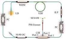
Passively mode-locked fiber lasers, featuring a compact structure, narrow pulse width, and rich nonlinear phenomena, provide an ideal platform for ultrafast laser research owing to their wide range of biomedicine, generation of terahertz radiation, investigation of attosecond dynamics, and communication. Following years of research, a variety of passively mode-locked techniques have been developed and successfully employed to generate ultrashort pulses, such as nonlinear polarization rotation, nonlinear multimode interference, nonlinear amplifying loop mirrors, Mamyshev oscillator, semiconductor saturable absorber mirror, and two-dimensional material. As a typical nonlinear system, the passive mode-locked fiber laser produces pulses that are subject to many factors, including gain, loss, dispersion, nonlinear effects, and spectral filtering. Examples of such phenomena include dissipative solitons or conventional solitons generated under normal or anomalous group velocity dispersion conditions, respectively, and dissipative soliton resonances arising from inverse saturable absorption effects. Similarly, spectral filters, which enable the manipulation of pulses by limiting spectral broadening and promoting intracavity dissipation, are of crucial importance in the context of mode-locked fiber lasers. The state of solitons can be controlled to evolve towards soliton molecules and pulse splitting by bandpass filters or fiber Bragg gratings. The utilization of Lyot filters or multimode interference filters facilitates the generation of sinusoidal spectral filtering within the cavity, which in turn enables the formation of h-shaped pulses, multi-wavelength pulses, and pulses with high repetition frequency. Nevertheless, the majority of the above reports pertain to a singular evolutionary route of pulse, which significantly restricts its applicability in many application scenarios. To move the pulses towards different evolutionary routes within the same laser configuration, we constructed a hybrid mode-locked ytterbium-doped fiber laser based on NPR and SESAM. The saturable absorption effect provided by SESAM enables pulse generation and the sinusoidal spectral filtering provided by NPR enables pulse shaping. Adjusting the polarization controller changes the strength of the spectral filtering. When the spectral filtering is weak, a dissipative soliton mode-locked pulse with a central wavelength of 1 036.64 nm, a 3-dB bandwidth of 1.96 nm, and a pulse width of 17.97 ps is produced. Further adjustment of the polarization controller results in the generation of asynchronous dual-wavelength pulses with central wavelengths of 1 033.22 nm and 1 037.06 nm, corresponding to a repetition frequency difference of 720 Hz. When spectral filtering is strong, it limits the soliton broadening, and the laser is capable of outputting multi-wavelength synchronized mode-locked pulses, with the number of wavelengths switchable from a single wavelength up to seven wavelengths. The analysis of the two pulse evolution routes serves to enhance our comprehension of hybrid mode-locked fiber lasers and offers a novel avenue for the generation of ultrashort pulses exhibiting multiple wavelengths or high repetition frequency.
Mar. 25, 2025Vol. 54 Issue 3 0314001 (2025)
Peng ZHANG, Jianwen WENG, Qing KANG, and Jianjun LI
Obtaining accurate, resolved and traceable reference solar spectral irradiance variations is of great research significance and application value in the fields of solar physics, atmospheric physics and environmental science. However, the high-precision solar spectral irradiance data available domestically and internationally generally has a low resolution, while the high-resolution reference solar spectral irradiance has a low precision, and the acquisition of high-resolution solar spectral irradiance data usually faces the problems of sampling difficulty, time-consuming sampling, and limited data precision.To address this problem, we propose a deep learning-based approach to reconstruct high-resolution spectral irradiance by analyzing a large amount of low-resolution spectral irradiance data. Our approach is based on a novel end-to-end fully convolutional residual neural network architecture that employs a new loss function, and by training the CNN model, we can learn the spectral features of the solar radiation to achieve high-resolution reconstruction of the solar spectral irradiance. This method utilizes the advantage of CNN in spectral feature extraction, which can fully exploit the feature information of high-resolution spectra. In our experiments, we first select the visible band (311.4~949.4 nm) of the HSRS high-resolution spectral dataset to add noise to expand the data to 5 000 spectra, and then convolve all the data with the Line Shape Function (LSF) with the SIM instrument to resample them into spectral data consistent with the low-resolution spectral resolution of the TSIS-1 SIM. Our CNN model is designed with some key improvement strategies to better accommodate the feature extraction requirements of high-resolution spectral reconstruction. The CNN spectral super-resolution network consists of a fully connected layer, a one-dimensional convolutional layer, a nonlinear layer, eight residual blocks, a one-dimensional convolutional layer and a cascade of nonlinear layers. The network was trained and tested on an Intel i7-12650H 2.30 GHz processor and an NVIDIA RTX 4060 graphics card, and the TensorFlow was used as a development framework for neural networks. In the training phase, a new loss function was used to better reconstruct the features of the spectra, which is a weighted sum between the Euclidean distances of the original and reconstructed spectra as well as their first and second order derivatives. The loss function was optimized using the Adam optimizer to optimize the loss function, with every 8 sets of spectral data as a batch, and every 1 000 batches for validation. If there is no improvement after more than 10 validation attempts, stop the training. Validation was performed on a randomly selected batch of spectra in the validation set and the average Spectral Angle Mapping (SAM) between the input and the reconstruction was used as a metric for validation loss. The reason for using the average SAM rather than the Root Mean Square Error (RMSE) as a measure of validation performance is that the SAM better compares the metric of spectral shape. During the testing phase, the reconstruction was performed using the average of the TSIS-1 SIM solar spectral irradiance measurements in the visible band from December 1-7, 2019, fed into a neural network. The reconstructed 0.1 nm solar spectral irradiance essentially overlapped with the official 0.1 nm solar spectral irradiance curve reconstructed using the spectral ratio method, with a SAM of 0.002 1, a MAPE of 0.636 6%, and the reconstruction time is only 0.942 1 s. This study shows that the proposed convolutional neural network can learn the solar spectral irradiance and its measurement instrument features well, which is conducive to accelerating the reconstruction speed of the solar spectral irradiance and expanding the scope of application of the solar spectral irradiance for high-precision space-based observation.
Mar. 25, 2025Vol. 54 Issue 3 0330001 (2025)
Qingyan HAN, Shixing FAN, Bochao ZHAO, Zihan LIU, Hao ZHANG, Wei GAO, Chengyun ZHANG, Zhiyu ZHANG, Sicong LIU, and Jun DONG
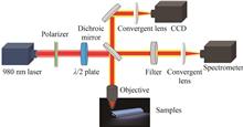
Lanthanide-doped Upconversion Luminescent (UCL) materials have attracted significant attention due to their distinctive optical properties, including excellent photostability, large anti-stokes shifts, high signal-to-noise ratios, and long emission lifetimes. These characteristics make UCL materials highly suitable for a wide range of applications, such as white light-emitting diodes, solid-state laser, and liquid crystal displays. Recently, white light emission from lanthanide-doped UCL materials has exhibited significant potential for applications in three-dimensional backlight technology. Upconversion white light is generally achieved by fine-tuning the emission intensities of red, green, and blue light. The red and green emission can be effectively modulated by varying the concentrations of Er3+ or Ho3+ ions, while the blue emission intensity is directly influenced by the concentration of Tm3+ ions. However, the effective regulation of the UCL spectrum and a deep understanding of its emission mechanisms remain significant scientific issues. Most researches on UCL have focused on the optical properties of micro/nanoparticle ensembles, where the collected spectra reflect an averaged emission effect from a large number of luminescent particles. Due to interparticle interactions, these measurements cannot accurately represent the emission behavior of individual crystal particles, making it even more challenging to uncover the fundamental photophysical mechanisms at the single-particle level. Therefore, exploring the luminescent properties of single lanthanide-doped upconversion crystal is crucial for the development of new materials and the optimization of their performance. In this work, we fabricate β-NaYF4:20% Yb3+/x%Er3+/0.2%Tm3+ (x=0.2,0.4,0.6,0.8,1.0) microcrystals the uniform morphology and size, featuring a natural hexagonal cross-section and wedge-shaped on both top vertexes. The microcrystals have an average length approximately 40.2 μm. Based on a selt-built confocal microscopy system, the upconversion luminescence performance of a single β-NaYF4:20% Yb3+/x%Er3+/0.2%Tm3+ (x=0.2,0.4,0.6,0.8,1.0) microparticle is detected and studied. A gradual shift in the UCL color of a single β-NaYF4 microcrystal from yellow-green to white was observed as the doping concentrations of Er3+ ions increased under 980 nm laser excitation. The upconversion luminescence emission of individual microcrystal primarily originates from the transitions of Er3? ions: 2H11/2/4S3/2→4I15/2 (520 nm and 539 nm, green) and 4F9/2→4I15/2 (653 nm, red), and the transitions of Tm3? ions: 1D2→3F4 and 1G4→3H6 (450 nm and 475 nm, blue), 1G4→3F4 and 3F3→3H6 (650 nm and 696 nm, red). In β-NaYF?:20% Yb3?/x% Er3?/0.2% Tm3? (x=0.2,0.4,0.6,0.8,1.0) microcrystals, the intensities of red and green emissions increase with the increasing Er3? ion concentration, while the blue emission intensity decreases rapidly with higher Er3? ion concentration. Ultimately, white light UC emission was successfully realized mainly due to competitive energy transfer between Yb3+→Er3+ and Yb3+→Tm3+, as well as cross-relaxation process between Er3+ and Tm3+ ions. Furthermore, the UCL polarization characteristics of a single β-NaYF4:20%Yb3+/0.2%Er3+/0.2%Tm3+ microcrystal were systematically investigated under the linearly polarized light excitation. As the polarization angle varies from 0° to 360°, the upconversion luminescence intensity of a single β-NaYF4:20%Yb3+/0.2%Er3+/0.2%Tm3+ microcrystal exhibits periodic changes. When the laser polarization direction aligns parallel or perpendicular to the long axis of the microcrystal, the upconversion luminescence intensity of the single microcrystal reaches maximum and minimum, respectively. Additionally, by tuning the excitation light focused on different positions of a single microcrystal, the UC white light emission intensity exhibited obvious periodic variations as the excitation polarization direction and the angle between the microcrystal’s wedge-shaped end and the slide were adjusted. These results demonstrate the strong dependence of the UCL intensity on the polarization of excitation light in the single β-NaYF4:20%Yb3+/0.2%Er3+/0.2%Tm3+ microcrystal. This research provides valuable insights into the spatial orientation and luminescence mechanisms of single anisotropic upconversion micro/nanocrystals and holds significant implications for advancing applications in anti-counterfeiting technologies and efficient fluorescent probes for bioimaging.
Mar. 25, 2025Vol. 54 Issue 3 0330002 (2025)
Huibin ZHAO, Yanli LI, Wensi LV, Xiangdong KONG, Li HAN, and He ZHANG
Atomic Layer Deposition (ALD) is a gas-phase deposition technique based on surface self-limiting chemical reaction. Thin film is deposited on the substrate by streaming precursor and purge gas into the chamber alternatively. Compared with other film growth method such as chemical vapor deposition or physical vapor deposition, due to the self-limiting growth characteristic of ALD, it can realize the deposition of thin film on curved substrate with good conformality and uniformity without additional operations including rotating the substrate. ALD is expected to enable the growth of high-quality film on curved substrate. For example, glass X-ray monocapillary is an important X-ray optics and is a hollow tubular structure with the advantages of drawing into required shape easily and small roughness of inner surface. X-ray focusing beam can be obtained by the total reflection of incident X-rays on the inner surface of monocapillary. It, has been widely used in synchrotron radiation large-scale scientific system and X-ray analytical instruments. According to its working principle, the preparation of a uniform, smooth film with density higher than that of glass on the inner surface of monocapillary can further expand the application of the monocapillary in the field of high-energy X-rays.Although ALD has the potential to grow uniform film on the inner surface of monocapillary, the ALD process has to be optimized specially to achieve uniform film growth due to the large aspect ratio of monocapillary. It can be known that the key to preparing high-quality film on the inner surface of monocapillary is to ensure that the chemisorption of precursor is saturated on the entire inner surface and that the excess precursor or by-product is purged away by analyzing the process of growing thin film by ALD. Therefore, prolonging the precursor streaming time and purge time are commonly used. However, due to the fact that only a small portion of the precursor gas is used for film growth and a large portion of the precursor is discharged from the chamber outlet, prolonging the precursor streaming time will lead to a long preparation time and a waste of precursor.In this paper, we investigated a different way to obtain high-quality film on the inner surface of monocapillary without prolonging the precursor pass-through time. Firstly, three coating models were designed by adjusting the number of inlet and outlet in ALD chamber and the connection of monocapillary tube to the outlet. In Model 1 the monocapillary tube was placed in the center of the chamber without any other treatment. In Model 2 the monocapillary tube was placed on the outlet side of the chamber and connected to one of the outlets so that some of the gases had to pass through the monocapillary tube before being extracted from the connected outlets. In Model 3, the monocapillary tube was placed on the outlet side of the chamber and connected to two of the outlets and the rest of the outlets are all covered, that is, all of the extracted gases must pass through the monocapillary tube before leaving the chamber. Secondly, Fluent was used to numerically simulate the flow of gases through the monocapillary tube under three different models and the distribution, diffusion process of gases in the monocapillary were discussed respectively. Each ALD cycle of HfO2 was carried out through a 9∶1 mixture of nitrogen and TDMAH pulse of 0.02 s, nitrogen purge of 30 s, a 9∶1 mixture of nitrogen and DI water pulse of 0.02 s and nitrogen purge of 30 s. Lastly, a model for the growth of high-quality HfO2 film on the inner surface of monocapillary was obtained. Besides that, HfO2 coated-monocapillary were prepared by ALD technique based on the three models and morphology of the films was characterized and analyzed.In brief, the process of growing HfO2 thin film on the inner surface of monocapillary tube with large aspect ratio by ALD method was investigated using Fluent simulation. The flowing process of gases inside the monocapillary tube was simulated and analyzed under three different models. The steady-state simulation results show that compared with Model 1, there are enough precursors in Model 2 and 3 to realize the saturated chemisorption on the whole inner surface along the monocapillary and HfO2 film with uniform thickness probably be obtained. The transient simulation results show that, compared with Model 3, excess precursors or by-product can be purged completely during the 30 s purging process in Model 2 and HfO2 film with smooth surface probably be obtained. Therefore, the simulation results show that Model 2 is a better coating model suitable for growing high-quality film on the inner surface of monocapillary with large aspect ratio. It lays theoretical foundation for growing HfO2 film by ALD method. The experimental results show that the HfO2 film prepared under Model 1 has a smooth surface but uneven thickness, the HfO2 film prepared under Model 2 has a smooth surface and a uniform thickness and the HfO2 film prepared under Model 3 has a uniform thickness but a very rough surface. They are in agreement with the simulation results and analysis. It can be known that changing the number of inlets and outlets as well as the connection of monocapillary to the outlet is an effective and cost-saving way to improve the film quality on inner surface of monocapillary.
Mar. 25, 2025Vol. 54 Issue 3 0331001 (2025)
Yonggang PAN, Youde WANG, Xiuhua FU, Zhaowen LIN, Xin DU, Haifeng XIE, and Peng SHI
Quantum communication is to construct protocols and algorithms using the Heisenberg Uncertainty principle of quantum mechanics, the No-Cloning theorem of quantum states and quantum entanglement properties to realize confidential communication in the real sense. Quantum communication is mainly divided into two kinds of quantum invisible transmission and quantum key distribution, of which the quantum key distribution technology is the most mature development, has been verified by researchers in various countries, and realized engineering applications. Restricted by the curvature of the earth and the loss of optical fiber, the ground-based quantum communication method can not achieve a wide range of quantum communication network coverage, so people will focus on the satellite platform, through the establishment of a highly stable and low-loss quantum channel between the satellite platform and the optical ground station, it can realize the ultra-long-distance quantum key distribution. The reflection element is an important part of the quantum key distribution system, which has the roles of efficiently transmitting optical energy and folding the optical path. When light is incident obliquely to the reflection element, the effective refractive index of the membrane layer for the p-polarized component and the s-polarized component is different, which generates the polarization effect and phase difference, leading to an increase in the quantum bit error rate; and when the light passes through the reflection element with the surface shape error, the different optical ranges experienced by the reflection on the surface lead to the distortion of the phase such as the wavefront, which influences the quality of coherent mixing and the efficiency of the communication coupling. Therefore, in order to improve the communication quality and reduce the bit error rate, the reflection element is particularly important to reduce the phase difference and surface shape error under the premise of ensuring higher reflectivity. In this paper, a low-sensitivity film system structure is designed to realize the preparation of high surface shape phase modulation reflective elements by stress compensation and so on.Based on the basic theory of thin film design, the relationship equation of phase difference Δ with respect to the incident angle θ, refractive index n and film thickness d at the wavelength λ position of a single-layer film is deduced. According to the principle of equivalent layer, the multilayer dielectric film can be equivalent to a single-layer dielectric film, and the phase difference Δ of the multilayer film can be calculated by changing the number of layers of the film system and the thickness of the film layer to obtain different equivalent refractive indices and equivalent phase thicknesses, so as to realize the precise regulation of the phase difference; combined with the optimization methods of the Essential Macleod software, such as Optimac, Nonlinear Simplex, etc., the spectra and phase difference Δ are designed and optimized. The phase-regulated reflective elements with spectra and phase difference meeting the usage requirements were designed.Based on the sensitivity analysis method, the sensitivity of the film thickness to the phase difference is studied, and the analysis shows that the sensitivity of the first 32 layers of the film is low, and the sensitivity of the 33rd and 34th layers is very high, and then ±1% of the film thickness error is introduced to the 33rd and 34th layers, respectively, and the phase difference still meets the requirements, which determines the feasibility of the design of the film system preparation.Film preparation using electron beam ion-assisted deposition method, the test can be obtained reflective element at 45° incidence, 632.8 nm ± 5 nm band reflectivity of 87.92%, 1 540 nm band p-reflectivity is 99.73%, s-reflectivity is 99.80%, the phase difference of 0.16°, 1 563 nm band p-reflectivity 99.74%, s-reflectivity 99.78%, phase difference of 0.16°, 1 563 nm band p-reflectivity 99.74%, s-reflectivity 99.78%, phase difference of 0.16°, the reflection element in the 45° incident. 99.74% p-reflectivity, 99.78% s-reflectivity, and 0.88° phase difference at 1 563 nm, which meets the spectral and phase difference requirements.Based on the stress balancing method, the same stress film layer is deposited on the back side to balance the stress of the front surface layer, which can realize the correction of the surface shape without affecting the spectra and phase difference of the deposited phase modulation reflective film. Combined with the SiO2 deposition experiment, the mathematical model of the change of reflective surface shape and the thickness of SiO2 deposition is established by linear fitting, and the thickness of SiO2 deposited on the backside of the reflective element is calculated for the optimal reflective surface shape, and the RMS of reflective surface shape error is corrected to 0.004 94 λ by depositing 4 805 nm SiO2 on the backside of the reflective element to realize the high-precision correction of the reflective surface shape. The calibration was realized with high precision reflective surface shape.According to the standard of GJB2485A-2019, the environmental adaptability test of the reflection was conducted, and the prepared reflection element passed the corresponding environmental adaptability test, which meets the requirements of the quantum key distribution system.However, there are still some problems in the development, and how to further reduce the sensitivity of the film layer to obtain a lower phase difference is the focus of the next step.
Mar. 25, 2025Vol. 54 Issue 3 0331002 (2025)
Shijie GAO, Zhen WANG, Xingxin FU, Wei LIU, Yongming MAO, and Jingtai CAO
To address the limitations of conventional optimization algorithms in Sensor-less Adaptive Optics (SLAO) systems, particularly the slow convergence and limited global search efficiency of Stochastic Parallel Gradient Descent (SPGD) algorithm and meta heuristic optimization algorithms, an Improved Dung Beetle Optimizer (IDBO) algorithm proposed by combining the Dung Beetle Optimizer (DBO) algorithm and the Osprey Optimization Algorithm (OOA) to significantly enhance wavefront correction in SLAO systems, achieving effective atmospheric turbulence suppression without the need for wavefront sensors. While the DBO algorithm is known for its strong optimization ability and fast convergence speed, it suffers from an imbalance between global exploration and local exploitation. To address this issue, we incorporate the Osprey optimization algorithm strategy to improve global exploration and enhance the local exploitation ability.The proposed methodology involves a model of an adaptive optics system using a 32-element deformable mirror for wavefront correction. The IDBO algorithm integrates the OOA to enhance the traditional Dung Beetle Optimizer (DBO), increasing population diversity and global search capabilities. Performance evaluations were conducted under various turbulence levels, utilizing wavefront aberrations as correction targets. We performed comprehensive comparisons of DBO, SPGD, and SA-SPGD algorithms, focusing on convergence speed, correction efficiency, and local extrema resistance. To evaluate the dynamic correction performance of the IDBO algorithm under different intensities of atmospheric turbulence, we conducted 20 simulations of the IDBO algorithm for atmospheric turbulence correction, with each numerical simulation introducing initial atmospheric turbulence of varying intensities.Numerical simulations results show notable improvements at an initial RMS value of 0.825 4, the IDBO algorithm achieves wavefront correction speeds that are approximately 14.0, 3.5, and 1.3 times faster than DBO, SPGD, and SA-SPGD, respectively. Under higher turbulence (initial RMS of 1.772 1), IDBO maintains superior performance with speeds 7.4, 1.1, and 0.8 times faster than the same algorithms. The system consistently delivers an 80% improvement in correction speed across different turbulence conditions while ensuring equivalent correction efficacy. IDBO also demonstrates enhanced convergence stability and robustness, significantly reducing the likelihood of entrapment in local extrema. The IDBO algorithm performs excellently under both weak and strong turbulence conditions. This hybrid algorithm has the advantage of rapidly correcting aberrations caused by turbulence of different intensities, resulting in better adaptive correction capability. The qualitative simulation results show the phase distribution before and after correction under weak and strong turbulence conditions.The integration of the OOA algorithm crucially improves algorithm performance by preserving diversity in the dung beetle population, averting premature convergence to local optimum solutions. The numerical simulations validate that the IDBO-based SLAO system outperforms mainstream algorithms in real-time control applications. With convergence speed, robustness, and dynamic correction performance amidst evolving turbulent conditions, IDBO algorithm presents a viable solution for wavefront correction in SLAO systems. This advancement offers a new approach to overcoming challenges in sensor-less adaptive optics, highlighting potential applications where traditional systems may falter. In the future, we intend to develop a high-performance processing platform based on FPGA and GPU, and apply the IDBO algorithm to dynamic aberration correction experiments.
Mar. 25, 2025Vol. 54 Issue 3 0306001 (2025)
Xinghua TU, and Haiyang ZHAO
Positioning algorithms based on visible light communication can help solve the problem of insufficient positioning accuracy in some special occasions such as indoors, basements, and underground. However, the accuracy of existing visible light positioning algorithms is difficult to improve further, and most of them remain in the simulation stage without experimental verification. In the previous visible light positioning algorithms based on deep learning, such algorithms can be divided into positioning algorithms based on received light signal intensity and positioning algorithms based on light source images according to the source of data. The positioning algorithm based on received light signal intensity receives the light signal intensity from each LED light source in turn, and obtains the positioning result based on the characteristics of the light signal intensity. Similarly, the positioning algorithm based on light source image receives the LED light source image and obtains the positioning result by analyzing the characteristics of the light source. This article proposes a positioning algorithm (MIF-VLP) based on the attention mechanism to fuse light Signal Intensity Information (RSS) and image information. The MIF-VLP algorithm uses ResNet-18 as the backbone network of the image, and maps RSS into a vector through word embedding, and then adjusts the output of ResNet-18 to make them have the same dimension. The fusion method of the attention mechanism is based on the image, so the input of the attention layer is multiple vectors, and the output is only one vector. The advantages of the algorithm are that, firstly, the algorithm uses both the light signal intensity information and the image information, which makes up for the overfitting problem caused by the single data, improves the generalization ability of the model and the final positioning accuracy. Secondly, the algorithm performs a permutation and combination preprocessing on the received light signal intensity, treats the input light signal intensity as a sequence, ignores the order and number of light signal intensities from multiple LEDs, and reduces the dependence on the environment to a certain extent. The traditional positioning algorithm based on the intensity of received light signals has strict requirements on the input order and number of data, because each light signal intensity represents the characteristics of an LED. In addition, the MIF-VLP algorithm can expand the size of the data set under the same experimental environment, so that the model can converge in fewer epochs and improve the generalization performance of the model. In comparison, the article selected the RSS-BP algorithm based only on RSS data and the CNN algorithm based only on light source images in the experimental stage. The CNN algorithm also uses ResNet-18 as the backbone network. The experimental results show that in the experimental environment of 2 m×2 m×1.8 m, the average positioning error of the MIF-VLP algorithm reaches 5 mm, which is 80.7% higher than that of the RSS-BP algorithm based on RSS information and 87.5% higher than that of the convolutional neural network algorithm based on image information; the maximum positioning error of the MIF-VLP algorithm reaches 8.9 cm, which is 41.4% lower than that of the RSS-BP algorithm based on RSS information and 19.1% lower than that of the convolutional neural network algorithm based on image information. The minimum positioning error of the MIF-VLP algorithm reaches 0.5 mm, which is much lower than the 1cm positioning error of the RSS-BP algorithm and the 2 mm positioning error of the CNN algorithm. Overall, among all the positioning points, the MIF-VLP algorithm has only one point with an error greater than 2 cm, which shows the stability of the MIF-VLP algorithm. Analysis shows that the reason for the large error at this point may be due to reflection or measurement error, because this point is located at the edge and is easily affected by reflected light.
Mar. 25, 2025Vol. 54 Issue 3 0306002 (2025)
Yi CHEN, Bo GAO, Linlin FU, Xiaowei WANG, Haijun ZHU, Jiangtao LIU, Zhentao ZHONG, Yongzheng LI, Linfeng GUO, and Xiaomin XU
With the continuous development of distributed optical fiber sensing technology, the Brillouin Optical Time Domain Reflectometry (BOTDR) system, due to its single-ended monitoring characteristics, electromagnetic interference immunity, and real-time sensing capabilities for temperature/strain changes, has become increasingly applied in structural health monitoring fields, particularly in large infrastructures such as bridges, dams, and subway tunnels. However, the weak spontaneous Brillouin scattering limits the performance of the BOTDR system. Increasing the input optical pulse energy enhances the scattering effect; however, if the energy exceeds a certain threshold, stimulated Brillouin scattering can deplete the pulse energy rapidly, reducing the sensing distance and impacting the system's performance. Factors such as the length, type, and condition of the distributed sensing fiber, as well as the linewidth and power of the light source in the BOTDR system, affect the stimulated Brillouin scattering threshold. Therefore, how to optimize the system's detection performance under varying stimulated threshold conditions is a key issue for compact and cost-effective BOTDR systems in practical engineering applications. This paper presents an automated detection method for identifying stimulated Brillouin scattering in optical fibers. The technique leverages Short-Time Fourier Transform (STFT)?-based optoelectronic demodulation and advanced signal processing. Its primary goal is to optimize the sensing distance for localized Stimulated Brillouin Optical Time-Domain Reflectometry (BOTDR) systems.The method uses an optoelectronic demodulation device to collect the raw time-domain Brillouin scattering signal along the fiber to be tested, applying STFT processing to obtain the Brillouin Gain Spectrum (BGS). By analyzing the peak intensity distribution of the BGS, a Brillouin peak intensity map along the fiber is plotted. A moving average method is used to remove random noise, followed by polynomial fitting to obtain the first- and second-order derivative curves. The zero-crossings of the second-order derivative are identified to locate the potential stimulated Brillouin scattering points. The first-order derivative values at these points are compared with a preset threshold σ to confirm the actual location of stimulated Brillouin scattering. To improve accuracy, the RMSE of the Brillouin peak intensity distribution in the denoised fiber section is calculated. The difference between the maximum and minimum values is computed and then divided by the window length h to derive the error threshold σ for linear fitting.In a 2 000 m fiber with a 20 ns pulse width and 20 kHz frequency, when the EDFA1 output power is 0.69 mW, stimulated Brillouin scattering occurred at a specific location of 1 230.2 m. The root mean square error of the Brillouin Frequency Shift (BFS) along the fiber indicated a deterioration in the signal-to-noise ratio after stimulated scattering, validating the effectiveness of the proposed signal processing method. The study further investigated the effects of pulse width, frequency, and fiber length on the location of stimulated scattering. Using a 2 000 m fiber with a 50 ns pulse width and 20 kHz frequency, with EDFA1 output power at 0.876 mW, the stimulated scattering occurred at 1 500.2 m. For a 2 000 m fiber with a 20 ns pulse width and 10 kHz frequency, with EDFA1 output power at 1.197 mW, the stimulated scattering occurred at 1 090.2 m. For a 1 009 m fiber with a 20 ns pulse width and 20 kHz frequency, with EDFA1 output power at 0.69 mW, the stimulated scattering occurred at 780.2 m. The results indicate that reducing pulse width or frequency advances the stimulated scattering position. Additionally, temperature experiments were conducted with a 2 000 m fiber, heating it to 50 °C in a water bath at 300 m and 800 m locations. The specific location of stimulated scattering was found to be 1 170.2 m.Using this method, it is possible to further determine the optimal sensing distance for low-cost BOTDR systems that utilize localized stimulated scattering, specifically for applications at construction sites. It can guide the configuration of the optimal sensing fiber length, determine the stimulated scattering threshold for the system, and fully leverage the performance of low-cost BOTDR systems. It overcomes the cost and applicability limitations of traditional technologies in practical applications, providing an economic, efficient, and adaptable monitoring solution for Brillouin fiber sensing technology in engineering applications. This method meets the needs of various standard construction monitoring applications.
Mar. 25, 2025Vol. 54 Issue 3 0306003 (2025)
Yinxiang ZHANG, Yan FENG, Yilin ZHOU, Bo QU, Fengzhi ZHAO, and Hua ZHANG
The tactile perception of a flexible humanoid robotic finger is essential for advancing applications in the fields of intelligent robotics, human-computer interaction, and prosthetics. This work presents a novel multi-parameter sensing method using fiber Bragg grating embedded in a cantilevered robotic finger structure. It aims to address the challenges posed by strain and temperature cross-sensitivity in tactile sensing systems. By embedding a differential sensing array of fiber Bragg grating sensors into the robotic finger, the design achieves accurate, real-time measurement of tactile force, contact temperature, and contact position while maintaining robustness and flexibility.The robotic finger is designed to closely replicate the structural and functional characteristics of a human finger, providing both dexterity and adaptability. The cantilevered finger bone is fabricated from polylactic acid through 3D printing, ensuring lightweight and high-strength properties. Six fiber Bragg grating sensors are symmetrically embedded within the cantilevered structure in pairs to form a differential sensing array. This differential configuration allows for the temperature compensation by sensing the same temperature and the opposite strain. This design effectively decouples strain and temperature effects, significantly improving the reliability of the sensor readings under varying environmental conditions.To ensure high precision, each fiber Bragg grating sensor in the array was carefully calibrated. Calibration experiments were performed to determine the stress and temperature sensitivities of the fiber Bragg grating sensors. The experimental results revealed that the embedded fiber Bragg grating array achieved a stress sensitivity of 112.898 pm/N and a temperature sensitivity of 81.185 pm/℃. Furthermore, the sensors demonstrated excellent accuracy and stability across a wide temperature range (10~50 ℃), with a minimum average measurement error of -0.025 6 nm. These results confirm the effectiveness of the differential sensing array in distinguishing between the effects of strain and temperature, making the system suitable for the tactile sensing tasks in practical applications.In addition to force and temperature sensing, the robotic finger can accurately detect the contacting position. By extracting the standard deviation features of the central wavelength shifts from the fiber Bragg grating sensors, we employed a support vector machine algorithm to classify different contact locations. The classification model was trained on data collected from multiple contact points across the finger's surface. The dataset is divided into a 70% training set (105 samples) and a 30% test set (45 samples) to ensure that the model's generalization ability. The support vector machine-based model achieved a contact position classification accuracy of 95.5%, demonstrating the system's capability to perform precise contact detection. This high level of accuracy is critical for applications that require fine manipulation, such as robotic surgery, where precise tactile feedback ensures safe and effective operation, and advanced prosthetic devices, where accurate sensory information enhances the user experience.In conclusion, this work demonstrates that fiber Bragg grating sensing technology, when integrated into a flexible robotic finger structure, provides a highly effective solution for multi-parameter tactile sensing. The system can accurately measure force, temperature, and contact position, featuring a lightweight design and high flexibility. This technology holds broad potential applications, particularly in scenarios where precise and reliable tactile feedback is essential. These include not only robotic surgery and advanced prosthetics but also collaborative robotics and human-computer interaction systems. Future research will focus on refining the design of the sensor array, optimizing the algorithmic approaches for data processing, and exploring additional applications in environments that demand precise tactile sensing.
Mar. 25, 2025Vol. 54 Issue 3 0306004 (2025)
Zhen ZHOU, Shuna YANG, Bo YANG, and Hao CHI
Broadband Radio Frequency (RF) Arbitrary-waveform Generation (AWG) plays an important role in modern information systems, like high-speed optical communications, biomedical imaging, chemical coherence control, and advanced radar applications. Benefiting from a large bandwidth and compact configuration, the Time-domain Pulse Shaping (TPS) system provides possibilities for generating RF arbitrary waveforms based on the Fourier transform relationship between the input-output waveform pair. However, limited by the relatively low sampling rate and bit resolution of the Employed Electronic Arbitrary-waveform Generator (EAWG), the diversity and fidelity of the realized waveforms as well as its reconfiguration speed are constrained. To remove the EAWG′s limitation and realize dynamic real-time reconfiguration of RF waveforms, we propose and demonstrate a novel approach of RF arbitrary-waveform generation based on an improved TPS system with an integrated Dual Parallel Mach-Zehnder Modulator (DPMZM) and multi-tone inputs in this work. Different from the conventional TPS system, the proposed system is built using a mode-locked laser, a DPMZM, and a pair of conjugate dispersive mediums. One major difference lies in the employment of DPMZM, which can realize the Carrier-suppressed Single-sideband (CS-SSB) modulation mode to guarantee the one-to-one mapping from each frequency element to the output optical pulse. Another difference is the generation of the multi-tone RF inputs, which is provided by commercial sinusoidal signal generators instead of EAWG. Based on the Fourier transform relationship between the RF input signal and the output optical waveform, the spectrum of the applied multi-tone signals is linearly mapped into the temporal profile of the output optical signal, i.e., a list of discrete optical pulses with adjustable amplitudes and time intervals are generated. The following Photodetector (PD) and Low-pass Filter (LPF) detect and smooth the temporal envelope of optical pulses to realize the RF waveform generation. Note that the output optical pulses serve as the sampling points of the desired RF waveforms. In this design, by simply configuring the frequency spacing and amplitudes of the multi-tone RF inputs, the desired RF arbitrary waveform can be generated and reconfigured in real time.In order to verify the proposed RF AWG approach, a proof-of-concept experiment was successfully carried out. Firstly, the system dispersion matching was performed to ensure the fidelity of the output RF waveform. Secondly, the amplitude values of the three-tone input signals have been adjusted, a variety of customized waveforms were generated. Meanwhile, the frequency interval between adjacent frequency elements has been separately set as 4 GHz and 5 GHz, two square waveforms with different sampling rates up to 20 GSa/s have been achieved. The obtained results validate that the proposed approach can realize independent controlling over each sampling point of the desired output waveform by properly configuring the amplitudes, frequency interval or frequency values of the multi-tone inputs. In addition, the effects of higher-order dispersion from the dispersion medium on the fidelity of the output waveforms have been investigated. The simulation results show that as the input frequency increases, the peak amplitudes of the output pulses will decrease and the pulse width may slightly grow up. However, the amplitude deviation introduced by higher-order dispersion can be easily compensated by properly adjusting the power settings of the multi-tone inputs.In summary, a novel approach of RF arbitrary-waveform generation via TPS with an integrated DPMZM and multi-tone inputs has been proposed and experimentally demonstrated. By properly adjusting the DC bias of DPMZM, the CS-SSB modulation of RF input can be achieved, which guarantees the one-to-one linear mapping from each frequency element of RF input to the output pulses. Any desired waveform can be obtained by simply adjusting the frequencies or the amplitudes of the multi-tone inputs. Proof-of-concept experiments on different waveforms generation have been successfully carried out. Additionally, the impacts of higher-order dispersion on waveform diversity and fidelity are also investigated.
Mar. 25, 2025Vol. 54 Issue 3 0306005 (2025)
Shujun ZHENG, Hongjie LIU, Xianmiao XU, Junchao JIN, Jinyu WANG, Dakui LIN, Yi YANG, Xiao LIN, and Xiaodi TAN
Dennis Gabor's groundbreaking contributions in the 1 940 s initially illuminated the enigmatic and potentially boundless field of holography. Over the subsequent decades, through his relentless perseverance, he continuously deepened and refined the theoretical framework of this technology. Holography, once perhaps confined to the realm of scientific fancy, gradually evolved into a pivotal tool for exploring new horizons in information storage, led by Gabor's visionary guidance. As the 1960s dawned, the rapid advancement of science and technology paved the way for Van Heerden, who, with his prescient vision, boldly foresaw the vast potential applications of holographic technology in data storage. This idea, akin to a seed, swiftly germinated and flourished with the nourishment provided by laser technology. The emergence of lasers furnished the crucial light source necessary for holographic data storage technology, thereby transitioning holographic data storage from theoretical discourse to practical implementation and gradually positioning it as a shining star in the landscape of next-generation optical storage.The unique advantage of holographic optical data storage resides in its unprecedented capacity to store information in a three-dimensional space within the recording medium. This distinctive feature allows for the parallel writing and reading of data, in stark contrast to traditional two-dimensional data transmission methods. By adopting this three-dimensional storage approach, holographic data storage technology not only vastly enhances storage capacity but also markedly boosts data transmission speed. Consequently, holographic data storage demonstrates unparalleled superiority in addressing the challenges posed by the big data era. The core of holographic data storage technology hinges on the volumetric recording of spatial light wave distributions, ushering in an entirely novel mode of data page storage. Leveraging the selective properties of thick holograms, holographic data storage facilitates parallel data processing and multiple recordings within the same medium area, resulting in faster data transmission rates and higher storage densities. This technology not only transcends the confines of traditional optical disc storage but also pioneers new avenues in the realm of data storage.To date, the domain of holographic data storage has delved into a variety of devices and technical solutions, with off-axis and coaxial systems emerging as the two most central system architectures. Furthermore, technologies rooted in computer-generated hologram and self-referencing have sequentially emerged, providing fresh momentum to the advancement of holographic data storage technology. As research continues to deepen, holographic data storage technology has made significant progress in multiple dimensions, including data recording density, data transmission rate, data storage security, environmental tolerance, and rewritable media. To further enhance the recording density of holographic data storage, researchers have proposed various innovative methods, among which multiplexing technology is key to achieving high storage density.Volume holographic data storage technology, leveraging the Bragg selectivity of volume holographic gratings, enables the storage of multiple sets of data at the same location within the storage medium, with each data page being individually readable. The implementation of this technology hinges on two primary categories of methods: spatial multiplexing and orthogonal/incoherent multiplexing. Spatial multiplexing techniques, specifically angle multiplexing and shift multiplexing, accomplish multi-address storage of information by adjusting either the angle or the relative position between the reference light and the object light. This approach effectively harnesses the storage volume, ultimately enhancing storage density and efficiency. To address the significant crosstalk noise issue in spatial multiplexing technology, researchers have introduced orthogonal/non-correlated coding multiplexing strategies for reference light. This strategy, based on the fundamental physical properties of light waves, has promoted the development of amplitude coding, phase coding, and polarization coding multiplexing technologies. By adjusting the pattern parameters of the reference light, multiple holograms can be stored in a superimposed manner, and through carefully designed grating superposition, only a specific diffraction efficiency is maximized, thereby effectively reducing crosstalk noise and enhancing the storage efficiency of the system.It is noteworthy that these multiplexing technologies do not exist in isolation but can be integrated and applied together to further promote the increase in storage density. When combined with multi-dimensional modulated data information, holographic data storage technology is expected to achieve unprecedented storage densities. Looking ahead, with the continuous progress of materials science, optical engineering, and information technology, holographic data storage multiplexing technology will continue to make new breakthroughs and contribute more to the informatization process of human society. Beyond the traditional application field of data storage, holographic multiplexing technology also exhibits broad application prospects in areas such as three-dimensional display, augmented reality, and optical communications. These emerging applications will not only further enrich the connotation of holographic data storage technology but also inject new vitality into the development of the world economy. Therefore, we have reason to believe that holographic multiplexing technology will play an increasingly important role in the future, becoming an important force in driving scientific and technological progress and economic development.
Mar. 25, 2025Vol. 54 Issue 3 0309001 (2025)
Zedong HUANG, Shaolan ZHU, Yiyi ZHAO, Jinyou TAO, and Jianfeng YANG
The rapid development of LiDAR technology has made the accuracy and stability of waveform decomposition critical factors limiting its practical application. Traditional waveform decomposition optimization algorithms face challenges such as sensitivity to initial conditions and insufficient fitting stability, which hinder the in-depth application and widespread use of full-waveform LiDAR across various fields. This paper focuses on optimizing the waveform decomposition algorithm for full-waveform LiDAR. The primary objective is to address key issues, such as sensitivity to initial values and poor fitting stability, present in traditional algorithms, thereby significantly enhancing the accuracy and stability of waveform decomposition.Regarding the research methodology, a decomposition model based on the Gaussian function is initially constructed. For the collected LiDAR echo data, a multi-step preprocessing procedure is applied. A wavelet denoising algorithm is employed to eliminate background noise, and the five-point cubic smoothing method is used to enhance the smoothness of the data. Building on this, the Gaussian inflection point method is implemented to provide a preliminary estimation of the initial parameter values. Following this, the parameter optimization process begins. This paper introduces the Differential Evolution and Levenberg-Marquardt (DELM) optimization algorithm for waveform decomposition. The Differential Evolution (DE) algorithm is first used for preliminary optimization. After determining the population size and dimensionality, the DE algorithm randomly generates individuals in the decision space, and through iterative processes such as mutation, crossover, and selection, it converges toward the optimal solution. Subsequently, the Levenberg-Marquardt (LM) algorithm is applied for secondary optimization of the DE algorithm results. The LM algorithm calculates the iteration step size based on critical components such as the objective function, Jacobian matrix, and damping factor, accurately updating the parameters, and decides whether to accept the update based on predefined criteria. This iterative process continues until the termination condition is met. The entire process is guided by the objective function, which minimizes the gap between the fitted and the collected waveforms.To collect abundant echo data, a fixed plate and target plates with different reflectivity are positioned at specific distances in front of the LiDAR, and the position and reflectivity of the target plates are adjusted. Additionally, to simulate a more complex and realistic application scenario, multiple obstacles are introduced between the fixed plate and the target plate, successfully collecting multi-target composite echo waveform data.The experimental results indicate that, in terms of fitting accuracy, the DELM algorithm demonstrates superior performance, far exceeding that of both the LM and DE algorithms. In most cases, the fitting correlation coefficient surpasses 0.97, and for selected representative echo waveform datasets, the fitting evaluation index exceeds 0.99. This strongly supports the ability of the DELM algorithm to accurately restore the waveform. In terms of stability, the standard deviation of the fitting correlation coefficient for the DELM algorithm is exemplary. Regardless of varying reflectivity or distance conditions, the DELM algorithm consistently achieves stable, high-quality waveform fitting. With respect to ranging accuracy, the DELM algorithm achieves an accuracy of 70 mm, which can be further reduced to 40 mm under optimal conditions. In contrast, the LM algorithm achieves an accuracy of 1 cm, and the DE algorithm achieves 90 mm, highlighting the significant advantage of the DELM algorithm.The proposed DELM optimization algorithm effectively addresses the inherent limitations of traditional algorithms, achieving a breakthrough in both fitting accuracy and stability. Fully validated through rigorous experimentation in both simple and complex environments, this algorithm offers substantial improvements in the ranging performance of LiDAR.
Mar. 25, 2025Vol. 54 Issue 3 0312001 (2025)
Daqi ZHANG, Yun ZHONG, Tao CHEN, Yu ZHANG, Yubin SHI, Jinhai SI, and Xun HOU
Hard and Brittle Materials (HBMs) such as diamond, sapphire, and quartz glass are employed in many applications within the aerospace, military, integrated circuits, biomedicine, and optoelectronic devices sectors. This is due to their high hardness, high thermal stability, chemical inertness, and excellent optoelectronic properties. In particular, hard and brittle materials play an indispensable role in the extreme environment of strong radiation and easy corrosion. Moreover, due to its high hardness and chemical inertness, employing traditional processing techniques to fabricate micro-nano structures is challenging. The pulse duration of femtosecond lasers is significantly shorter than the time scale of electron-lattice interaction, which enables the preparation of micro-nano-structures in a nearly heat-affected region. The existence of the femtosecond Laser Damage Thresholds (LDT) effect enables the spatial resolution of laser processing of hard and brittle materials to be greatly enhanced. Consequently, the study of the LDT of materials is of great significance, as it allows the spatial resolution of femtosecond laser processed materials to be enhanced and provides a reference for the processing scheme.There are three principal methods for obtaining LDT the direct measurement method, the model calculation method and the extrapolation method. The direct measurement method is well-suited to initial material LDT testing due to its simplicity of operation and the ability to obtain data quickly. However, the LDT of the material is related to the parameters of the laser, such as wavelength, pulse width, repetition frequency and the type of focusing objective of the laser process, which requires a significant amount of measurement work. Furthermore, the presence of local defects or inhomogeneities in the material can lead to early damage, introducing uncertainty into the results of experiments conducted using the direct measurement method. Consequently, a significant number of experiments are required to verify the results. Additionally, the discontinuity of processing parameter settings necessitates a substantial number of experimental determinations to accurately obtain the LDT. The model calculation method, which predicts the LDT by computer simulation of the laser-material interaction process, circumvents the necessity for extensive experimental validation, provides precise prediction of the LDT and elucidates the underlying physical mechanism. However, the mechanism of femtosecond laser-material interaction is complex, and it is challenging to develop an accurate physical model. Furthermore, the intricacy of the physical model renders it costly to compute, while its high demand for parameter precision renders it more challenging to align with the actual processing environment. Extrapolation is a method of deriving the LDT by discovering the relationship between laser processing parameters and damage morphology. One of the most commonly used methods is the method of extrapolating the LDT from the diameter of the damage. The extrapolation method combines the advantages of the direct measurement method, which avoids the problem of the existence of an early ablation area of the material by measuring the diameter of the damage area with a certain area, with the simplicity of operation of the extrapolation method. This method then uses the relationship between the processing parameters and the diameter of the damage area to predict the LDT of the material, which avoids a large number of experiments and reduces the cost of measurement. Nevertheless, in the event of manual measurement, there is a risk of inconsistency in measurement standards and manual reading errors, which may result in a reduction in the efficiency, reliability and comparability of threshold results.In this paper, a novel methodology for the automatic measurement of femtosecond laser damage threshold is proposed. The proposed methodology is based on image recognition algorithm and is designed to meet the demand for laser damage threshold measurement on the surface of diamond and other materials. The methodology involves the use of microscopic images of the damage structure in grey scale, the application of a binary Fourier filter to denoise the images, and the automatic extraction of the damage region's boundary. This is achieved by means of an algorithm. The damage structure is then identified automatically, and its area is measured. The damage area and laser power logarithmic curve are then fitted, and the damage threshold value is extrapolated. Utilizing this methodology, the single-pulse damage threshold of the 50-fs femtosecond laser is determined to be 3.1 J/cm2 for single-crystal diamond, and the single-pulse damage threshold of microcrystalline diamond is established as 0.55 J/cm2 for microcrystalline diamond film. The reliability of the method was verified by the comparison of field emission scanning electron microscope, atomic force microscope and identification results. The method is deemed suitable for materials exhibiting uniform and stable surface morphology and laser damage features that differ from the original surface. The adoption of a uniform and controllable identification standard has been demonstrated to significantly reduce randomness and instability in the measurement process, thereby improving the credibility of the measurement results. Furthermore, the automation of the data processing process enhances measurement efficiency and reduces costs, providing a valuable reference framework for femtosecond laser processing of materials. The development of deep learning, real-time monitoring and high-speed imaging technologies is expected to lead to more intelligent recognition, more efficient real-time feedback and a wider range of material applicability, providing strong support for high-precision processing and quality control of femtosecond lasers in scientific research and industry.
Mar. 25, 2025Vol. 54 Issue 3 0312002 (2025)
Hongyang WANG, Zijing ZHANG, Hao LIU, Xinran LYU, Jiayu SONG, Chengshuai CUI, and Yuan ZHAO
In the remote detection of the rotational velocity of a target, the vortex beam is easily affected by the random atmospheric turbulence, which causes the phase distortion of the beam and the dispersion of OAM spectrum, resulting in the deterioration of the performance of rotational velocity measurement. Since Wirtinger flow algorithm was proposed, its remarkable feature is that it can complete iterative convergence without any prior information and only one input, without falling into local optimal solutions. Relevant studies have theoretically shown that Wirtinger Flow algorithm has the ability of high precision and absolute convergence to the global optimal solution. The current research has improved the performance of the algorithm by enhancing the traditional WF algorithm. However, the analysis of improving the rotational velocity measurement metrics through compensating the beam distortion in complex environments is still insufficient.To solve this problem, this work enhances the traditional WF algorithm by improving the initialization and gradient descent rules, and proposes Truncated Weighted Wirtinger Flow (TWWF) algorithm. In this algorithm, the median value of the sample is introduced into the truncation rule in the initialization stage to make the initial estimation closer to the global optimal. The weight adjustment strategy of the weighted gradient descent algorithm is used to calculate the weight coefficient according to the results of adjacent iterations, and the distorted vortex beam is compensated to improve the optical field and the rotating Doppler frequency shift characteristics.Firstly, a vortex light field recovery and rotation velocimeter performance improvement system based on TWWF algorithm is designed. The input is simplified into one path. The probe beam then passes through the coded aperture of a programmable LCD screen, simulating a coded diffraction pattern, and then the CCD measures the light intensity for algorithm calculation, and finally the generated compensated phase screen is loaded on the spatial light modulator. The results show that when the atmospheric turbulence intensity Cn2 is 1×10-14 m-2/3, the purity, RDS peak-to-maximum sideband ratio and velocity measurement accuracy can reach 0.99, 2.18, 0.80 rad/s. When Cn2 is 1×10-12 m-2/3, it can reach 0.74, 2.09, 0.83 rad/s, and the phase relative error can reach the order of 3×10-16, which demonstrates the powerful compensation ability of TWWF algorithm. In addition, the influence of mask number, superposition state of optical field and other factors on the algorithm metrics is discussed. More masks can provide more phase information, accelerate the convergence speed and prevent the algorithm from falling into the local minimum, improve the global search ability of the algorithm, make the algorithm more accurate and reliable phase recovery, and improve the stability and accuracy of phase recovery. Considering that more masks increase the computational complexity and time cost, it is appropriate to choose L=40, it balances these factors effectively, the purity is 25 times that of L=5, and the velocity measurement error is 57.76% of that of L=5. For vortex beam superposition state, TWWF algorithm also shows excellent compensation ability, P, SMSR, σ can be stable at 0.49, 3.19, 0.54 rad/s. This study further broadens the application of WF type algorithm in the direction of turbulence distortion compensation, and provides a method to improve the remote velocity measurement performance of vortex beams.
Mar. 25, 2025Vol. 54 Issue 3 0312003 (2025)
Huiling LIU, Xingxing HAN, Bei ZHAO, Bing GAO, and Jiajie WANG
The physical and chemical properties of particle materials are closely related to their particle size that the measurement of particle size distribution plays an important role in a wide of applications in chemical industry, environmental protection and other fields. Among the various particle size measurement methods, the forward laser scattering technique has been widely used because of its advantages, including high efficiency, high precision, good repeatability and non-intrusive measurement. The problem of retrieving particle size distribution based on spatial distribution of light scattering intensity belongs to the first Fredholm integral problem, which is difficult to give an analytical solution, which was typically solved by numerical inversion methods. Due to the influence of ambient light noise and circuit noise on light energy distribution signal, the inversion of particle size distribution with high accuracy is one of the key issues in this technique. The inversion methods are generally divided into two kinds: independent mode method and non-independent mode method. The independent model method does not need to know the particle size distribution information in advance, which can theoretically obtain the particle size distribution of any particle system. However, such methods suffers from its sensitivity to noise and the width of the particle size distribution, which might cause distortion in the results. The non-independent mode method needs to assume that the particle size distribution meets a certain distribution function based on the prior information of particle size distribution, and then solve the problem on the basis of the set distribution function model. Compared to the independent mode method, this kind of method has advantages in computation efficiency and anti-noise ability. The traditional intelligent algorithm can obtain good inversion results when dealing with unimodal distribution particle system. However, for the cases where the particle size distribution of the particles presents a bimodal or multimodal pattern, the optimization parameters in the inversion process increases a lot, resulting in an exponential increase in inversion computation. Traditional inversion algorithms suffer from problems such as rapid decline in optimization efficiency, rapid deterioration of robustness and inversion accuracy. Regarding the inversion problem of particle size distribution in the forward laser scattering measurement technique, an improved whale optimization algorithm was proposed in this paper by using a logarithmic form of adaptive probability threshold and non-linear convergence factor, which balancing its ability in global search and local optimization in the inversion optimization process. By using reverse learning method for initialization and greedy principle for individual updates, an accurate and fast inversion of particle size distribution can be achieved. The simulation results show that the algorithm has a good robustness and inversion accuracy for unimodal and multimodal distributions that follow normal distribution, Rosin-Rammler distribution, or Johnson's SB distribution under different levels of random noise. The proposed algorithm was applied to the practical experimental measurement using standard spherical polystyrene particles, very good inversion results were obtained, verifying the effectiveness of the algorithm in terms of noise resistance and measurement accuracy.
Mar. 25, 2025Vol. 54 Issue 3 0312004 (2025)
Lili GUO, Zhenhuan HAN, Xuezhu LIN, and Lijuan LI
Traditional laser projection systems face significant challenges when projecting onto large objects, mainly due to their limited projection range. Projection errors are positively correlated with parameters such as projection angle and projection distance, and it is not advisable to increase the projection distance to extend the projection range. Furthermore, if the projection environment is relatively narrow, it is impossible to extend the projection range by increasing the projection distance. Frequent station changes and repeated calibration are required. This limitation leads to the need for multiple recalibrations to position the projected object, which requires the arrangement of complex cooperative target points and increases the calibration time, which greatly reduces the overall efficiency. To solve these problems, this study introduces an innovative omnidirectional industrial laser projection positioning system that integrates a dual-axis turntable, which can project 360° without the need for repeated calibration, thereby improving projection efficiency and expanding the effective projection range. For the omnidirectional industrial laser projection positioning system integrating a dual-axis turntable constructed in this paper, a calibration method based on the four-axis rotation angles of both the dual-axis galvanometer and the dual-axis turntable is proposed. First, a calibration model is established for the system construction parameters, which are the relative poses between the 3D laser projection system and the dual-axis turntable. In principle, calibration only needs to be performed before the unit leaves the factory or when accessories are replaced, and does not need to be repeated in the field. Specifically: 1) use a laser tracking system to separately position the dual-axis turntable and the multi-parameter integrated calibration plate to obtain the relative pose of the laser tracker with respect to each of the two; 2) use the laser 3D projection system to position and calibrate the multi-parameter integrated calibration plate to obtain the relative pose between the two; 3) the relative pose between the dual-axis turntable and the laser 3D projection system, i.e. the system construction parameters, can be obtained from the above relative pose relationship. Next, three sets of cooperative target points were set up in three different directions, with two cooperative target points in each set. The rotation angles of the dual-axis galvanometer of the laser 3D projection system and the pitch and roll angles of the dual-axis turntable were recorded when calibrating each set of cooperative target points. Based on the four-axis rotation angles of the dual-axis galvanometer and dual-axis turntable corresponding to different cooperative target points, a system external parameter calibration model is established. Based on the dual-axis turntable coordinate system, the relative pose between the laser 3D projection system coordinate system and the projected object coordinate system is obtained and the pose change is monitored in real time. Finally, an objective optimisation function is constructed for the calibration model, and a sequential least squares optimisation algorithm is used to solve for the calibration parameters. According to the working characteristics of the omnidirectional industrial laser projection system, such as the projection range and the distance of the projector, the starting point is chosen close to the feasible solution domain. A multi-start strategy and the current value of the objective function are used to find the global optimal solution, ensuring accurate determination of the calibration parameters. For the above strategy, the RMS value of the error calculated by the six cooperative target points is used as a reference. The results of 100 repeated calculations using the above algorithm show that the above strategy is sufficient to allow the algorithm to find a solution with global optimal properties for the problem given in this paper, and the calculation meets the accuracy requirements of the simulation. The accuracy of the calibration model was verified by simulation, and the simulation results showed that the theoretical accuracy reached 10^-6 mm. Under the simulation of normal distribution errors, the average calibration accuracy of the system was maintained at 0.242 mm. The experiment of system construction parameter calibration verified the stability and accuracy of the verification system construction parameter calibration. By causing the dual-axis turntable to rotate a fixed angle, the relative pose between the laser 3D projection system and the dual-axis turntable after the rotation of the dual-axis turntable was calibrated and the dual-axis turntable, comparing it with the relative pose between the laser 3D projection system and the dual-axis turntable after the rotation of the dual-axis turntable obtained by solving the system construction parameter calibration model, and calculating the absolute deviation (translation matrix and rotation matrix) between the two. The experimental results show that the absolute deviation of the rotation matrix of the two positions can reach the level, and the absolute deviation of the translation matrix can reach 0.023 mm. To verify the omnidirectional projection accuracy, a system external parameter calibration experiment was designed. Three multi-parameter integrated calibration plates were used to simulate the scene of projection and positioning of a large projected object. The experimental results further proved that the system can dynamically adjust the posture of the 3D laser projection system relative to the projected object through the dual-axis turntable, thereby achieving omnidirectional projection (360°). The maximum position deviation is about 0.30 mm, which meets industrial accuracy standards.
Mar. 25, 2025Vol. 54 Issue 3 0312005 (2025)
Hao MIAO, Yang ZHANG, Xianghua YU, Dan DAN, Junwei MIN, Yanlong YANG, Jia QIAN, and Baoli YAO
The observation of three-dimensional (3D) structures of objects provides much more specific information to the biomedical research. As a new kind of 3D fluorescence microscopy, Light-Sheet Fluorescence Microscopy (LSFM) uses a thin light-sheet to selectively excite the fluorescence signal of samples from the side, and collects the signal in the orthogonal direction, enabling its intrinsic optical sectioning ability. Compared to the conventional Epi-fluorescence microscopy, LSFM only illuminates the in-focus area and minimizes the phototoxicity and photobleaching, making it very suitable for long-term imaging for living specimens. Besides, LSFM uses CMOS or CCD sensors to capture the image plane-by-plane, possessing the merit of high-speed imaging rate. Therefore, LSFM has been broadly applied in the fields such as cell biology, neuroscience, developmental biology, etc. However, commercial light-sheet fluorescence microscopes are normally bulky and expensive, and thus are usually placed in the shared equipment center where researchers have to queue up for their time-consuming experiment appointments. The delicate biological samples may degrade or expire during transportation, which is negative to the investigation. What's more, to improve the image resolution of LSFM, many researches have managed to combine LSFM with other super-resolution microscopies, such as Structured Illumination Microscopy (SIM), Single-Molecule Localization Microscopy (SMLM), but at the cost of further increasing the size and the expense of the system.In this paper, we designed and built a compact multicolor light-sheet fluorescence microscope. In the illumination path, a 1D scanning galvanometer is used to scan the Gaussian beam to generate the Gaussian light-sheet, and a Dove lens is added to change the orientation of the light-sheet to make it coincide with the focal plane of the detection objective. In the detection path, a detection objective and a tube lens are used to collect and image the fluorescence signal with the sCMOS camera. The volume of the system is only 30 cm(L)×30 cm(W)×40 cm(H), which is merely about 1/5 of that of the Zeiss's Lightsheet7 light-sheet fluorescence microscope. To improve the spatial resolution of the system, we used the Mean Shift Super Resolution (MSSR) algorithm to process the acquired data. As a computational super-resolution method, MSSR can recover a super-resolution image from a single frame of fluorescence image without the need of additional optical and mechanical components, facilitating the spatial resolution improvement of the compact light-sheet fluorescence microscope. The lateral resolution of the system is 530 nm, which can be improved to 330 nm after using the MSSR algorithm. We conducted imaging experiments on the spinach root slice and the rat intestine slice. With the 3D multiple field-of-view stitching technique, a dual-color 3D fluorescence image of the rat intestine slice is achieved with the field-of-view of 2.75 mm×3.35 mm×1.55 mm (4 180×5 100 pixels@850 slices). The results show that the system can realize super-resolution fast multicolor 3D fluorescence imaging of biological samples, providing a useful microscope for the biomedical researchers.
Mar. 25, 2025Vol. 54 Issue 3 0318001 (2025)
Taiyuange LOU, Chengxiang GUO, Tong YANG, Lei YANG, and Hongbo XIE
To address the specific requirements of particle image velocimetry systems in microscopic imaging applications, particularly focusing on the challenges encountered when commercial microscopes fail to meet the demands for long working distance, high resolution, and integrated design, a novel 30×fluorescence detection microscope with a long-working-distance apochromatic objective lens specifically tailored for micro-PIV measurements is developed.The design process employs refractive design principles and an infinity-corrected structure to ensure high-quality imaging across a broad visible light spectrum (400~800 nm). The illumination system is designed to provide uniform and stable light, which is critical for capturing high-quality fluorescence images. The imaging components, including the objective lens, tube lens, and filters, are meticulously arranged to achieve a compact and user-friendly system. The optical design has been optimized to minimize various aberrations, including chromatic and spherical aberrations, ensuring that the overall imaging performance approaches the diffraction limit. Methods for increasing the working distance and techniques for apochromatic correction are proposed. The main way to increase the working distance is to adjust the focal length and interval of the negative light group and the positive light group. The method of apochromatism is mainly replacing glass materials and combining them. After optimization, a numerical aperture of 0.35, a working distance of 17.3 mm, and a microscopic objective with a magnification of 30 times were formed, which exceeded the limitations of conventional microscopic objectives. Additionally, the mechanical design of the microscope emphasizes robustness and ease of use, with the entire system weighing approximately 17.29 kg and measuring 360 mm×300 mm×300 mm. The entire microscope system is designed to be portable and lightweight, enabling remote operation capabilities. It features excellent sealing properties, allowing it to be deployed in complex environments while minimizing stray light interference. Additionally, the displacement stage provides a user-friendly interface for observing various microfluidic channels, enhancing the system's versatility and usability in diverse experimental settings.Upon completion of the optical and mechanical designs, the optical lens and mechanical structure of the complete system are manufactured. After assembling and building, the system undergoes rigorous testing and evaluation. Initial tests involve imaging a USAF standard resolution target to assess the optical resolution of the microscopic system. The results demonstrate that the microscope achieves a resolution greater than 228 lp/mm, corresponding to a line width of 2.2 μm, which meets the required specifications for micro-PIV applications. Subsequently, the system is employed in micro-PIV experiments on a microfluidic chip containing fluorescent particles with a velocity of nearly 1 m/s. The particles are illuminated with a 532 nm laser, and a double-exposure camera captured the resulting fluorescence at 613 nm through a 550 nm high-pass filter. The captured images display clear and distinct particle images, even for particles as small as 1 μm in diameter, confirming the high resolution and sensitivity of the system. These particle images are then processed using a Fourier transform-based cross-correlation algorithm to analyze the velocity field within the microfluidic chip. The algorithm calculates the displacement of particles between two consecutive frames and derives the velocity vectors based on the time interval and magnification factor. The velocity distribution obtained from the experiments shows excellent agreement with theoretical simulations, with a deviation of less than 6% between the measured velocities and the simulated values.The optical and mechanical design of the proposed microscope meets the stringent requirements for high resolution, long working distance, and integrated functionality. The experimental results validate the feasibility and effectiveness of the system, demonstrating its capability to provide clear and accurate particle images and reliable velocity measurements. This work can offer a valuable reference for the development of specialized microscopic imaging systems.
Mar. 25, 2025Vol. 54 Issue 3 0318002 (2025)
Huimin HONG, and Wenjun HE
Micro-LED, renowned for its exceptional brightness, energy efficiency, and rapid response times, has shown immense potential in the display technology sector, particularly in light of the ongoing advancements within the semiconductor industry. The detection of defects in the wafer is a crucial step in the production of Micro-LED, as it guarantees the dependability and excellence of the final product. The core technology underpinning the wafer defects detection system, which is microscopic visual online inspection, aids in the stable detection of product defects. Regrettably, the limitations in spectral range, field of view, and spatial resolution of current commercial microscopic objectives present a significant challenge in meeting the stringent high-precision and rapid detection demands for Micro-LED wafer defects. Based on our analysis of the system's operational requirements, the microscopic objective for the automatic optical inspection system intended for detecting defects in Micro-LED wafer must encompass a wide spectral range, offer a large field of view, achieve high spatial resolution, and maintain a considerable working distance. We established the design specifications and selected the camera based on the resolution and field of view criteria of the microscopic objective, aligning with international standards for microscopic objective. Considering the design priorities of a large field of view and a long working distance, the microscopic objective is structured as a retro-telecentric system, comprising three optical groups with positive, positive, and negative focal lengths for the front, middle, and rear groups, respectively. The angle ratios between the optical groups were established as Δu1: Δu2: Δu3=0.8∶ 0.7∶ -0.5, in order to minimize the considerable light deviation between lenses and to ease the structural design and adjustment. Utilizing the multi-group combination calculation formula, we calculated the focal lengths of the optical groups to be φ1=0.025 mm-1, φ2=0.020 mm-1, and φ3=-0.017 mm-1. Considering that the front group introduces a Schmidt surface to reduce spherical and coma aberrations while avoiding excessive field curvature and astigmatism; the middle group uses single lenses and cemented lenses, with the cemented lenses incorporating anomalous dispersion glass to eliminate chromatic aberrations and secondary spectra, and a meniscus lens to correct field curvature while also compensating for the spherical and coma aberrations introduced by the front group; the rear group uses a combination of positive and negative cemented lenses to further compensate for the field curvature, coma and astigmatism introduced by the front and middle groups, and other off-axis aberrations. The coordinated interaction of the front, middle and rear groups achieves the correction and balance of aberrations. Based on the focal power distribution and the characteristics of the components in each optical group, we designed the initial optical system. We then used Zemax to perform preliminary optimization on the system to ensure that the first-order performance metrics met the design specifications. However, due to the influence of secondary spectra, MTF values across different fields of view were rather modest and did not reach the diffraction limit when accounting for wide-spectrum chromatic aberration correction. To address this, we employed the Buchdahl dispersion model, which converges faster than the standard Sellmeier and Schott models, to investigate the dispersion properties of glass. Dispersion coefficients of CDGM glass were computed using Matlab. The dispersion vector sum G0 was utilized to assess the level of chromatic aberration correction in the optical system. Ray tracing of the initial optical system was used to determine the modulus of the dispersion vector sum of the initial structure, which guided the replacement of glass materials and achieved chromatic aberration correction in the initial optical system design. Ultimately, we developed a wide-spectrum, large-field microscopic objective composed of 11 easily manufactured, high-frequency glass components. It has a spectral range of 420 nm to 1 064 nm, a field of view on the object side of 3.3 mm, a focal length of 20 mm, a numerical aperture of 0.34, a working distance of 8 mm, a resolution of 0.88 μm in the visible light band and a resolution of 1.35 μm in the near-infrared band. A performance comparison with five typical 10× microscopic objectives from companies such as Mitutoyo and Olympus reveals that the developed wide-spectrum, large-field of view objective offers significant benefits in spectral breadth, imaging field of view, and numerical aperture. Image quality evaluation results indicate that the microscope objective corrects chromatic aberration over the entire spectral range and has a flat field of view with overall image quality near the diffraction limit. The tolerance study confirms that the objective meets both image quality and manufacturing standards for microscope objectives. This microscopic objective covers the spectrum from the visible light band to the near-infrared band, and with its large field of view and high-resolution imaging capabilities, it can effectively enhance the detection accuracy and efficiency of surface and subsurface defects in Micro-LED wafers.
Mar. 25, 2025Vol. 54 Issue 3 0318003 (2025)
Manzhuo WANG, Zhentao YAO, Chaoyang SUN, Yue ZHANG, Jimin FANG, Xiaoqiang SUN, Yuanda WU, and Daming ZHANG
Optical communications have advantages of low-loss long-distance transmission, large bandwidth and capacity. However, due to the existence of nonlinearity and dispersion, the Single-mode Fiber (SMF) communication networks is closing to the theoretical upper limit (~100 Tbit/s). Some multiplexing technologies, including Wavelength Division Multiplexing (WDM), Polarization Division Multiplexing (PDM), and Space Division Multiplexing (SDM) are adopted to increase the capacity. Due to the bandwidth restriction of optical amplifier and nonlinear effect of fiber, the WDM technique is approaching its capability ceiling. The limited polarization states in the PDM technique cast barriers to further enlarge the capacity, too. Recently, the SDM technology has been considered as a growing solution to expand the volume of fiber communications. Among SDM technologies, the Mode Division Multiplexing (MDM) can provide favorable data channels in one Few-mode Fiber (FMF) or multicore fiber. Different from the fiber transmission mechanism, the on-chip MDM technique has merits of compact size and functions integration.As a key device of on-chip MDM application, the mode switches play the role of mode conversion and routing. Due to the merits of compact size, large manufacturing tolerance and high mode Extinction Ratio (ER), the Multimode Interference (MMI)-based mode switches have been investigated, in which data exchange between different spatial channels can be implemented. These are considered as the Mode Selector Switch (MSS). Compared to reported mode switches that are implemented on the silicon or polymer platforms, silica technology has advantages of long-time stability, wideband transparence, compatibility to CMOS fabrication, and low-loss coupling with fiber. Therefore, silica waveguide is adopted in this work.According to the effective refractive index theory of the waveguide and the principle of MMI self-imaging, a silica waveguide mode selector switch constructed by cascading a 1×3 Multimode Interference (MMI) coupler and a 3×3 MMI coupler is proposed and fabricated. MMI-based mode switches have attracted wide attention due to their small size, large process tolerance, high Extinction Ratio (ER) and large bandwidth. The phase of the optical signal input to the 3×3 MMI coupler is changed by thermo-optic modulation, which can achieve the conversion from the input of the first-order mode (E10) to the output of the fundamental mode (E00) and selectively output from the target port. When the input is fundamental mode (E00), E00 can be output directly from the selected port. In addition, in order to enhance the efficiency of thermo-optical modulation and reduce thermal crosstalk, an air trench is used to concentrate the thermal field and increase the phase transformation amplitude, so that the heat can be concentrated in the waveguide core layer and reduce the additional power consumption caused by thermal diffusion.The switch is designed and optimized using the Beam Propagation Method (BPM) and fabricated using standard CMOS techniques including ultraviolet lithography, plasma etching and Plasma Enhanced Chemical Vapor Deposition (PECVD). The test results show that the first-order mode (E10) switches between the two output ports when the drive power is 170 mW and 395.3 mW, respectively. In the wavelength range of 1 523 nm to 1 556 nm, the insertion losses, crosstalks, and extinction ratios of the three output ports are≤10 dB, ≤-15 dB, and ≥15 dB, respectively. The switch has a rise time of 0.941 8 ms and a fall time of 1.042 ms. The proposed switch has a higher extinction ratio and lower crosstalk, which is mainly attributed to the cascaded MMI design and the precise waveguide fabrication process, so that the actual waveguide size matches the theoretical design value. In addition, the biggest advantage of silica waveguide switch is its long-term stable operation reliability, which is of great significance for the practical application and large-scale production of devices. The proposed mode selector switch has good potential in on-chip signal routing applications.
Mar. 25, 2025Vol. 54 Issue 3 0323001 (2025)
Yongchang DING, Xueyan LI, Yijian WU, Lieshan ZHANG, and Di CHANG
The large size of traditional optical lenses limits their application in compact image sensors. In recent years, graphene oxide metalens have promoted the development of optical lenses toward miniaturization and integration. Since the inherent diffraction properties of graphene oxide metalens lead to the phenomenon of chromatic aberration, optical zoom based on wavelength modulation can be realized by using chromatic aberration as a new dimension, which can achieve the effect of continuous repeatable zoom without moving the optical components and only by changing the wavelength of the incident light.In this paper, a wavelength-modulated axial zoom super-resolution graphene oxide metalens system design method based on a genetic algorithm is proposed. By utilizing the phase-amplitude dependence of graphene oxide and reduced graphene oxide materials, phase and amplitude are simultaneously modulated to achieve super-resolution focusing based on incident light wavelength modulation. In the operating wavelength range of 432~632 nm, the objective function is set to the incident light of different wavelengths has the maximum optical field intensity at the preset focal length, and the wavelength-modulated optical zoom can be realized by using this objective function. During the optimization design process, the radius of the graphene oxide metalens is fixed at 150 μm, and the numerical aperture can be increased by decreasing the focal length, which in turn improves the imaging resolution, so the optimization constraints of the minimum numerical aperture requirement are introduced, and by setting the minimum numerical aperture to 0.4, the super-resolution focusing can be achieved in the operating wavelength range of 432~632 nm. Genetic algorithms were then used to inverse design the ring structure parameters of the graphene oxide metalens based on the predefined objectives and optimization constraints. During the optimization process of the genetic algorithm, selection, crossover and mutation are continuously performed, and the algorithm will stop iterating when the convergence condition that the distribution of the radius of the reduced graphene oxide ring has not changed for 50 consecutive generations is satisfied. The final output is the optimal solution of the evolved population, that is, the best ring radius distribution, which not only meets the design requirements but also has stability and reliability. By utilizing the proposed genetic algorithm inverse design theory, we designed compliant zoom super-resolution graphene oxide metalens with a maximum ring radius of 150 μm, a total of 67 reduced graphene oxide rings, a graphene oxide film thickness of 200 nm, a reduced graphene oxide film thickness of 100 nm, a width of 0.8 μm for each ring, and a center distance of at least 0.9 μm between two neighboring rings to ensure that graphene oxide and reduced graphene oxide regions are distributed alternately. The simulation results show that the designed radial resolution of the zoom super-resolution graphene oxide metalens exceeds the diffraction limit of over the working wavelength range, while the focal length is adjustable with the working wavelength in the range of 201.6~318.8 μm, and the zoom range reaches 117.2 μm, and the simulation results are in favorable consistency with the theoretically pre-determined results. The maximum focusing efficiency is 82.07% and the average focusing efficiency is 57.53% over the whole working wavelength range, with favorable focusing spot uniformity, high focusing intensity and favorable consistency in the bandwidth from 442 nm to 592 nm. The designed zoom super-resolution graphene oxide metalens achieves fast, continuous, repeatable zooming and super-resolution focusing effects through precise modulation of the phase and amplitude of the incident light, which can be further applied to the study of micro-and nano-optics, and provides a new way for miniaturized, integrated, and non-mechanically movable optical zoom systems.
Mar. 25, 2025Vol. 54 Issue 3 0323002 (2025)
Shengxi JIAO, Xu YANG, and Hanrui YANG
The issue of energy has now risen as a key topic that human society needs to urgently address. Among these problems, solar energy is a common sustainable and environmentally friendly energy source. If solar energy is effectively tapped and applied, it can not only significantly reduce our dependence on conventional energy sources, but also help to alleviate the problem of environmental pollution. Solar absorber is an important component of solar energy utilization system that absorbs solar energy radiation and is essential to achieve high photothermal conversion efficiency. In this paper, a metamaterial solar absorber with a stacked circular nested cylinder is proposed, which is structured by a bottom metal and dielectric layer and a stacked circular nested cylinder in the upper layer. The absorption spectrum and electromagnetic field energy distribution of the absorber are studied and analyzed by the finite time domain difference method, as well as the effects of polarization angle and incidence angle on the absorption performance, and then analyzed by comparing the experiments for the effects of the structural dimensions of the absorber on the absorption rate. This design has potential application value in the field of solar energy absorption and utilization, and also provides research ideas for the design of broadband absorber. In summary, a solar absorber was designed by combining stacked and nested structures and its absorption characteristics were investigated. The FDTD method is used to investigate the effect of different geometrical parameters on the absorption properties. When applying the FDTD method to the calculation, the periodic boundary conditions in the x and y directions are set, while the boundary condition in the z direction is a Perfectly Matched Layer (PML), and the mesh step is set to be 10 nm. With regard to the dielectric constants of the materials, the dielectric constants of Ti, W, and SiO2 are referred to the experimental values of Palik. The substrate of the designed absorber is chosen as the substrate of the absorber, which is the most suitable for the absorber. In this paper, the substrate of the absorber is chosen as Ti, and the thickness of Ti is chosen as 300 nm, mainly because the thickness exceeds the skinning depth of light in Ti, so that the transmittance of the incident sunlight is 0, and then the absorbance size of the absorber is only related to the reflectance size. Then the optimum dimensional parameters of the other parts of the absorber are determined, and the optimized optimum parameters are the period P=50 nm, the inner radius of the metal ring R1=100 nm, the outer radius R2=190 nm, the lower SiO2 medium H1=H2=50 nm, the lower W-metal D=100 nm, the thickness of the upper metal ring t=d=40 nm, and the height of the medium cylinder h=220 nm. In order to analyze and verify the advantages of the stacked circular nested structure, comparative experimental verification is carried out. When the absorber has no nested cylindrical structure, there is a large downward fluctuation in its low band, and the average absorption rate in the whole band decreases to 92.21%; when the absorber has no stacked metal rings, there is a significant decrease in the whole band, and the lowest absorption rate decreases to 39.64%, and the average absorption rate is 74.82%; when the absorber is only set with a group of W/Ti rings, the absorber in the whole band absorption rate there is a decrease, the lowest absorption rate is 71.28%, and the average absorption rate is 91.35%. Comparative experimental results show that the designed solar absorber exhibits more efficient and stable absorption in a wide band. Under the optimal parameters of the structure, the absorber can maintain more than 88.51% absorption in the wavelength from 300 to 2 500 nm with an average absorption of 94.34%, and the relative bandwidth of the absorber is 156%. The results show that the absorber has polarization insensitivity and wide-angle absorption characteristics, and its average absorption is 88.81% under the tilted incidence condition of 60°. By comparing with other literature studies, although the average absorption rate of the absorber designed in this paper will be slightly lower than that of the absorber mentioned in the comparison, the large enough relative bandwidth can be more favorable for practical applications, and a comprehensive comparison of the average absorption rate and the relative bandwidth can be concluded that the absorber designed in this paper has an excellent performance. Combined with the electromagnetic field distribution, the analysis shows that the combination of stacked and nested structures has a certain degree of superiority, which can realize the broadband high absorption of solar radiation energy in the main concentration band. The broadband high absorption is mainly attributed to the nested structure of rings and cylinders, the surface plasmon resonance effect between the bottom dielectric layer and the metal layer, and the mutual coupling of multiple resonant modes. The fabrication of such nanodevices has become feasible with the continuous advancement of deposition and lithography technologies. This study provides an important reference for the optimization of the design of ideal absorbers, cloaking devices, and photovoltaic cells, and provides a new research direction for the effective absorption and conversion of solar energy.
Mar. 25, 2025Vol. 54 Issue 3 0323003 (2025)
© Copyright 2018-2021 | Chinese Laser Press.
All Rights Reserved 沪ICP备15018463号-20