


Please enter the answer below before you can view the full text.


2024
Volume: 44 Issue 11
36 Article(s)

jin Wang, feng Zhao, Yanqun Zuo, Yunfei Duan, Lingjie Kong, Qiang Qian, and Shuaishuai Hou
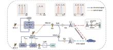
ObjectiveWith the continuous development of 6G technology and a series of high-speed new services such as big data, cloud computing, and autonomous driving, data can only be transmitted for a higher transmission rate and a lower transmission delay. Meanwhile, it is necessary to pursue high transmission quality to ensure sound communication performance, and high-precision speed measurement, ranging, imaging, and wide-area perception are also required. Under different application scenarios and changes in various performance indicators, further breakthroughs should be achieved in communication, with better results yielded than traditional communication systems. The terahertz frequency band integrates the advantages of microwave communication and optical communication and features a high transmission rate, large capacity, strong directionality, high security, and good penetration. On the one hand, in radar applications, since its wavelength is very short at about 30 μm-3 mm, much smaller than the wavelength of microwave and millimeter waves, it can be employed to detect smaller targets and realize more accurate positioning. On the other hand, it has a wide range of frequencies and a very broad bandwidth to transmit nanosecond and picosecond pulses at thousands of frequencies. As a new sampling theory, compressed sensing needs to be quickly applied to various fields, such as speech coding, image processing, and radar detection. By taking advantage of the sparsity of the signal, the signal sampling frequency will be much smaller than the minimum signal sampling rate required in Nyquistian’s theorem, and then a discrete sample of the signal will be obtained by random sampling. Finally, the signal is reconstructed by a nonlinear algorithm. Among them, the field of compressed sensing and millimeter wave channel estimation has also yielded good results. To achieve higher spectral efficiency and restore high-quality signals, we adopt the compressed sensing method to process the integrated signals in the integrated communication and sensing system to achieve high-speed and high-quality signal transmission and sensing.MethodsDigital signal processing is performed via MATLAB to generate communication signals and radar perception signals, which are converted into analog signals using digital-to-analog conversion devices, with the converted analog signals utilized to drive I/Q modulators. The I/Q modulator consists of two parallel Mach-Zehnder modulators. Then, the modulated signal is coupled with the external cavity lasers by the optically neutralized coupler, and the coupled signal is beaten via the photodiode. In the communication part, the signal is mixed with the local oscillator to downgrade the signal to the mid-frequency domain. The generated IF signal is converted into a digital signal via an analog-to-digital converter, and then the communication signal is recovered after digital signal processing. In the radar perception part, the integrated signal modulated by frequency division multiplexing is divided into upper and lower beams by the optical beam splitter, the upper beam is transmitted from the transmitter to space, and the receiver receives the echo signal. The echo signal and the downbeam signal are mixed and deskewed to obtain a single-frequency signal, which is adopted to drive the first MZM. Meanwhile, the pseudo-random sequence is employed to drive the second MZM modulator, and then the modulated signal is beaten and filtered to realize the Nyquist sampling process of the deoblique signal. Finally, the signal is reconstructed by the orthogonal matching pursuit algorithm to obtain the original signal.Results and DiscussionsIn the experiment, the communication transmission of 16QAM signal under 8 Gbaud or the communication rate of 32 Gbit/s is realized (Fig. 11). When the measurement distance is no more than 1.6 m, the error distance is kept within 2 cm (Fig. 16). In the 1 m wireless simulation experiment, when the power ratio of the communication signal to the sensing signal is 7, the power of the communication signal is much greater than that of the sensing signal. Thus, the performance of the communication link is the best, the bit error rate is 0.0093, and the distance measurement error is large because the power of the sensing signal is too low with an error of 4.12 cm. Under the power ratio of 0.125, the power of the perception signal is much greater than that of the communication signal, and the measurement distance error is 0.413 cm. However, due to the low power of the communication signal currently, its performance is poor with a bit error rate of 0.0633. The power ratio at the intersection of the two curves is 0.75, which is the best coexistence of communication and perception in the simulation experiment (Fig. 18).ConclusionsWe propose an integrated optical terahertz synaesthesia system based on compressive sensing and theoretically analyze the principle of integrated signal generation and reception based on compressed sensing. Based on the joint simulation of MATLAB and VPI, the communication and perception performance of the integrated signal, the performance boundary of the integrated synaesthesia, and the influence of the compressed sensing algorithm on the perception accuracy are analyzed. The results show that the 16QAM-LFM signal can achieve a communication rate of 32 Gbit/s, and the bit error rate is lower than the soft decision threshold of forward error correction. In the compressive sensing simulation experiment, when the data compression ratio is 4 and the measurement distance is less than 1.6 m, the distance measurement error is less than 2 cm. Meanwhile, due to the data volume compression, the performance requirements of the analog-to-digital converter are lowered.
Jun. 10, 2024Vol. 44 Issue 11 1106002 (2024)
Huiqin Wang, Weiyu Zhou, Qihan Tang, Zhen Wang, Pengfei Wu, Qingbin Peng, and yue Zhang
ObjectiveOptical orthogonal frequency division multiplexing index modulation (OOFDM-IM) is a novel multicarrier technique that achieves higher transmission rates by additionally adding mode order indexing via loading two different modes of constellation symbols on the active subcarriers and retaining the silent subcarriers. At the same time, the presence of silent subcarriers improves the bit error rate (BER) performance of the system. However, the presence of silent subcarriers also brings a waste of spectrum resources. Therefore, in this paper, a zero-padded dual-mode optical orthogonal frequency division multiplexing index modulation (ZDM-OOFDM-IM) is proposed to improve the transmission rate. Meanwhile, in order to solve the problem of excessive system detection complexity, a three-level stepwise detection algorithm based on K-mean clustering algorithm (KMC++) is proposed by combining the greedy (GD) algorithm, log-likelihood ratio (LLR) algorithm, and KMC++ algorithm.MethodsIn the ZDM-OOFDM-IM system, the active subcarrier was selected by the subcarrier index, and the constellation symbols of two different modes were mapped by the symbol information. Then, the modulation symbols were loaded on the active subcarriers according to the order index to complete signal modulation. After orthogonal frequency division multiplexing (OFDM) data block merging, inverse fast Fourier transform, non-zero clipping, and other processing, the light source sent it out. The optical signal transmitted through the atmospheric turbulence channel was received by the detector and could be restored to the original signal after processing by fast Fourier transform, subcarrier recovery, and maximum likelihood (ML) detection. According to the subcarrier index, constellation pattern order, and different characteristics of constellation symbols in the ZDM-OOFDM-IM system, GD, LLR, and KMC++ algorithms were used to detect the proposed detection algorithm, so as to reduce the complexity of the receiver signal detection. Finally, the feasibility of the system and the proposed algorithm were verified by the Monte Carlo method and experimental equipment.Results and DiscussionsIn this paper, the ZDM-OOFDM-IM system and its low-complexity novel detection algorithm are proposed, and its feasibility is verified through simulation and experimental devices. In addition, the influence of the key parameters of the system on the BER is analyzed. The results show that the ZDM-OOFDM-IM system can effectively improve the transmission rate, which gradually approaches the dual-mode OOFDM-IM with the increase in the subcarrier block length and the number of active subcarriers (Fig. 2). Moreover, at all modulation orders of 4, the signal-to-noise ratio (SNR) of the proposed system is improved by about 4.02 dB compared to DM-OOFDM-IM at BER of 3.8×10⁻³ (Fig. 4). In addition, when the subcarrier block length is fixed, increasing the number of active subcarriers can significantly increase the transmission rate but inevitably results in BER loss. When the number of active subcarriers is constant, an increase in subcarrier block length leads to an improvement in BER performance. For example, compared to the (4,2,1,2,4) system, the transmission rate of one frame of the (4,3,1,2,4) and (4,3,2,2,4) systems is improved by 64 bit/s and 128 bit/s, respectively, while their SNRs are lost by 2.17 dB and 2.26 dB at BER of 3.8×10⁻³, respectively. Compared with the (4,2,1,2,4), (4,3,1,2,4), and (4,3,2,2,4) systems at BER of 3.8×10⁻³, the SNRs of the (8,2,1,2,4), (8,3,1,2,4), and (8,3,2,2,4) systems are improved by 4.53 dB, 3.72 dB, and 2.50 dB, respectively (Fig. 5). The proposed algorithm achieves a BER that approximates the ML detection and eliminates the “plateau effect” of the conventional KMC algorithm (Fig. 6). Under the proposed algorithm, it is concluded that the increase in the modulation order leads to a significant increase in the transmission rate although it brings a smaller BER loss. For example, when ML detection is employed at BER of 3.8×10⁻³, the SNRs of the (4,2,1,2,2) and (4,2,1,4,4) systems lose 3.41 dB and 5.56 dB, respectively, compared to the (4,2,1,2,2) system, whereas the transmission rates of their one-frame signals are enhanced by 64 bit/s and 128 bit/s, respectively (Fig. 7). Moreover, in the experimental setup, the system BER and the performance of the proposed algorithm also achieve results consistent with the simulation (Fig. 9 and Fig. 10). Finally, the computational complexity of the proposed algorithm is given and compared with several classical decoding algorithms to demonstrate its computational complexity advantage (Fig. 11).ConclusionsIn order to solve the problem of unsatisfactory transmission rate and BER performance in the traditional wireless OOFDM-IM system, a ZDM-OOFDM-IM system is designed in this paper, which effectively enhances the transmission rate. Compared with the OOFDM-IM system, its transmission rate is increased by 96 bit/s for one frame of information when the number of subcarriers is 16, and the number of active subcarriers is 8. Meanwhile, in order to solve the problems of excessive ML decoding complexity and poor BER performance of other traditional detection algorithms, a three-stage stepwise detection algorithm is proposed by combining the GD, LLR, and KMC++ algorithms, which obtains a complexity close to that of linear decoding algorithms under the premise of guaranteeing the BER performance. Finally, the system successfully realizes wireless optical communication transmission with a BER of lower than 3.8×10⁻³ through the constructed indoor transmission experimental device, which verifies the feasibility of the system and the proposed algorithm.
Jun. 10, 2024Vol. 44 Issue 11 1106003 (2024)
Guoxiang Weng, Qinghua Tian, Fu Wang, Feng Tian, Qi Zhang, Leijing Yang, and Xiangjun Xin
ObjectiveWith the rapid development of optical communication technology toward high capacity, large bandwidth, and high speed, the multi-dimensional multiplexing technology is widely researched and adopted. Polarization multiplexing technology is an important multiplexing technique. However, polarization introduces damage to polarization multiplexing systems. In extreme weather conditions such as lightning near optical cables, the Kerr effect, and the Faraday effect, rapid rotation of the polarization state of the signal can be caused. This rotation disrupts the orthogonality of the two polarization states, thus increasing the bit error rate. Therefore, it is significant to trace and compensate for polarization state rotation. Currently, equalization algorithms for rotation of the state of polarization (RSOP) include the constant modulus algorithm (CMA), the Kalman filtering algorithm, and its derivative algorithms. The CMA is simple to implement but becomes ineffective when RSOP changes rapidly. In recent years, the focus has been realized by the Kalman filter and its derivative algorithms, including the extended Kalman filter (EKF), covariance Kalman filter (CKF), and square root covariance Kalman filter (SCKF). The EKF yields high tracking and compensation accuracy for RSOP but requires the calculation of the Jacobian determinant, which results in high algorithm complexity. The CKF avoids the computation of the Jacobian determinant, significantly reducing algorithm complexity. Although the SCKF avoids the positive definite decomposition of the state error covariance matrix in CKF, during the adaptive SCKF implementation, the process noise matrix still needs to calculate out positive definite decomposition, which cannot be fully guaranteed during the actual algorithm execution. We propose a new RSOP equalization algorithm based on adaptive square root cubature Kalman filtering. This algorithm avoids the positive definite decomposition of Q and exhibits adaptive updating of the noise covariance matrix in various scenarios, thus enhancing the algorithm’s robustness.MethodsA residual decision-adaptive square root cubature Kalman filtering based on the square root of Q(RD-ASCKF-SQ) algorithm is proposed for equalizing RSOP. This algorithm initiates a time update by calculating cubature points using the square root matrix of the state error covariance from the k-1 time or the initialized state parameter prediction. Subsequently, cubature points after the state transition are computed based on the state transition function to obtain the predicted state vector and the predicted square root of the state error covariance for the current time k. The next step is to proceed to a measurement update. The new cubature point set is calculated again from the state prediction in the previous step. Then the propagation cubature point is calculated according to the measurement transfer equation. Meanwhile, the predicted measurement values and the square root of the innovation covariance matrix at time k are calculated. Finally, by computing the square root of the self-covariance and cross-covariance matrices, the Kalman gain is obtained. The innovation is then calculated based on the error between the actual and predicted measurements. Additionally, combining the Kalman gain for signal recovery can yield the final state estimation, and residual decision detection can help decide whether the process noise Q should be updated.Results and DiscussionsWe conduct numerical simulations on a 112 Gbit/s PDM-QPSK system to validate the performance of the RD-ASCKF-SQ algorithm. Meanwhile, we perform simulation analyses to assess the performance differences between ACKF and RD-ASCKF-SQ under varying rates of RSOP changes. For RSOP azimuthal angle change rates ranging from 10 Mrad/s to 120 Mrad/s, the average bit error rate of RD-ASCKF-SQ is lower than that of ACKF. Additionally, the bit error rates of RD-ASCKF-SQ at different RSOP change rates all meet the 7% forward error correction threshold. Simulation analyses also examine the bit error rate curves of SCKF and RD-ASCKF-SQ under different signal-to-noise ratios (SNRs). In the statement of RSOP azimuthal angle change rate of 40 Mrad/s and low SNR, the SCKF algorithm fails to converge when the diagonal elements of Q are set to 10-2 and 10-4, and it achieves convergence only when the values are set to 10-6. In contrast, RD-ASCKF-SQ converges with Q diagonal elements set to 10-2, 10-4, and 10-6. RD-ASCKF-SQ exhibits greater tolerance to different initial Q values than SCKF, converging adaptively to appropriate values for RSOP equalization. The introduction of square root coefficients is analyzed for its influence on the convergence probability and average bit error rate of the ASCKF algorithm. Before the introduction of square root coefficients, ASCKF yields a convergence probability of 95% at RSOP azimuthal angle change rate of 70 Mrad/s and 94% at 80 Mrad/s. In contrast, RD-ASCKF-SQ consistently achieves a convergence probability of 99%. RD-ASCKF-SQ avoids the positive definite decomposition of Q, reducing algorithm complexity and further enhancing stability. Furthermore, we analyze the adaptive update counts of ASCKF and RD-ASCKF-SQ for RSOP azimuthal angle change rates ranging from 10 Mrad/s to 120 Mrad/s. RD-ASCKF-SQ exhibits fewer update counts at lower RSOP values, gradually increasing as RSOP values rise. Meanwhile, traditional ASCKF requires adaptive updates at every time step, and the update counts are independent of the algorithm’s convergence status. Compared to traditional ASCKF, RD-ASCKF-SQ reduces unnecessary adaptive updates, thereby improving algorithm runtime speed.ConclusionsWe propose an RSOP equalization algorithm based on RD-ASCKF-SQ. The basic idea of this scheme is to update the square root of the error covariance matrix directly by the square root coefficient. It avoids the positive definite decomposition of Q in each adaptive process. Additionally, it combines a residual decision detector to impose constraints on parameter updates. The algorithm updates Q when it diverges and stops updating when it converges, thereby improving running speed and reducing running time. The algorithm performance is validated by numerical simulations in a 112 Gbit/s PDM-QPSK system. The proposed algorithm demonstrates adaptive capabilities, showing higher robustness under improper Q selection than the SCKF algorithm. Additionally, compared to the ASCKF algorithm without square root coefficients, it exhibits superior stability. These characteristics hold across different scenarios, highlighting the algorithm’s commendable generalization performance.
Jun. 10, 2024Vol. 44 Issue 11 1106004 (2024)
Jianzhi Li, Yucheng Shi, Zhe Ji, Fei Xu, and Yanliang Du
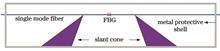
ObjectiveRailway transport is an important part of China’s transportation strategy and is still in the high-speed construction stage, with its total operation mileage reaching 1.59×10⁵ km. As the direct carrier of train operation, the inside and surface of rails will have a variety of defects and damages due to long-term operation and vibration shock. What’s worse, this will directly endanger the safety of trains and passengers if defects or damages are not found and repaired in time. At present, piezoelectric sensors are usually employed to detect ultrasonic rail damage and each of them needs a power line connection, which makes it difficult to achieve multi-point multiplexing detection. In contrast, optical fiber Bragg grating (FBG) has the unique advantages of electromagnetic interference resistance, easy reuse, and corrosion resistance, which makes it suitable for damage detection of long-distance structures such as steel rails in harsh environments. To detect ultrasonic waves, we propose and design a high-sensitivity FBG ultrasonic sensor based on a coupled dual-slant cone structure. Meanwhile, the optimal size of the sensor is analyzed and determined, with the sensor object made. The dynamic characteristics of the sensor are tested experimentally, with a new approach provided for long-distance structure ultrasonic detection.MethodsFirst, the optimal sensor size is obtained. Based on the mechanism of FBG and ultrasonic waves and the principle of slant conical energy accumulation, the slant conical sensor is modeled and solved by COMSOL simulation software 6.0. The amplitudes of ultrasonic signals detected by non-conical, positive conical, and slant conical structures are analyzed and compared respectively. The influence of slant conical structure parameters β, d, H, and i on the sensor performance is studied in detail. Then, three-dimensional (3D) printing technology is adopted to make the entity of the sensor device. After that, a narrow-band light source demodulation system is built to detect ultrasonic signals of different frequencies. Finally, the performance of PZT, bare FBG, and mono-clinic cone sensing devices is tested and compared.Results and DiscussionsSensor structure size is analyzed and optimized. The verification effect of angle β on the performance of the slant cone shows that when β=25°-35°, the pressure and x-axis displacement at FBG have larger values. The effect of the bottom diameter d on the performance of the slant cone shows that when β=30° and d=10 mm, the maximum pressure and displacement are 707 Pa and 1.7×10⁻⁷ mm respectively. The effect of base height H on the performance of the slant cone shows that when β=30°, d=10 mm, and H=12.5mm, the pressure and displacement have maximum values of 880 Pa and 2.4×10⁻⁷ mm respectively. Meanwhile, it is found that the slope i of the slant cone is also an important factor affecting the structure energy concentration. When i=1.138, the pressure at the tip of the cone is the maximum. By comparing the maximum and minimum values of different parameters, we find that each parameter has a great influence on the sensor performance. The maximum pressure is 880 Pa, and the minimum pressure is 47 Pa, with a difference of about 18.6 times. The maximum displacement is 2.4×10⁻⁷ mm, the minimum is 1.1×10⁻⁸ mm, and the difference is about 21.8 times. It is determined that the ideal size of the sensor is β=30°, d=10 mm, H=12.5 mm, and i=1.138. In this case, the cone has a strong ultrasonic focusing ability and a greater effect on ultrasonic detection improvement by FBG. A narrow-band light source system is built to detect sinusoidal ultrasonic signals. The experimental results show that the dual-slant cone FBG sensor has strong resolution and the ability to detect ultrasonic waves in the range of 20-150 kHz, and the response voltage has a good linear relationship with the drive voltage. In the detection frequency range of 40-60 kHz, the detection amplitude is 90-230 mV, the signal-to-noise ratio is 10-19 dB. The signal-to-noise ratio characteristics of bare FBG, single-slant cone ultrasonic sensing device, piezoelectric sensor, and dual-slant cone ultrasonic sensing device are compared. The test results show that the dual-slant cone and single-slant cone FBG ultrasonic sensors have a higher signal-to-noise ratio of ultrasonic signals than piezoelectric sensors in the frequency range of 40-70 kHz. The noise of piezoelectric sensors is relatively small at about 1-2 mV, which can achieve a high signal-to-noise ratio. In detecting sinusoidal ultrasonic signals above 80 kHz, the signal-to-noise ratio reaches a maximum of 30 dB, and the signal-to-noise ratio is higher than that of the ultra FBG sensing device. Compared with piezoelectric sensors, the slant cone FBG ultrasonic sensing device has significant advantages in detecting frequencies of 40-70 kHz.ConclusionsTo enhance the sensitivity and reuse of FBG ultrasonic sensors, we propose an FBG ultrasonic sensor based on a focusing coupling slant cone structure. Based on the analysis, a physical sensor prototype is fabricated and the dynamic properties of the sensor are experimentally tested. The research results reveal that the encapsulated dual-cone FBG ultrasonic sensor significantly improves the sensitivity of FBG in detecting ultrasonic waves within the frequency range of 20-130 kHz, and the detection amplitude is increased by about 21 times at 50 kHz. Additionally, the dual-cone sensor has remarkable characteristics of double-end output and strong reuse, which is suitable for applications in long-distance structural damage monitoring such as rails and bridges.
Jun. 10, 2024Vol. 44 Issue 11 1106005 (2024)
Xinyu Liu, Liping Chen, Yuming Chen, Yongzheng Li, Qiuming Huang, Yingkai Chen, Linfeng Guo, and Xiaomin Xu
ObjectiveThe distributed Brillouin optical time domain reflectometry (BOTDR) sensing system is based on the linear relationship between the frequency shift of spontaneous Brillouin scattering (SpBS) and temperature/strain on the optical fiber. It utilizes a convenient structure of single-ended incident light detection to measure temperature and strain along the fiber over long distances, reducing measurement complexity and application costs. Meanwhile, it allows for continued fiber detection even when the optical fiber is broken on an engineering construction site, avoiding the limitations associated with employing a double-ended loop Brillouin optical time domain analysis (BOTDA) sensing system after the fiber loop breakage. This makes the BOTDR system more practical in engineering applications. However, due to limitations imposed by stimulated Brillouin scattering (SBS), if only SpBS occurs in the system,the power can not exceed SBS’s threshold power. Consequently, the low incoming fiber optical power results in weak signal energy and a low signal-to-noise ratio (SNR) within the system, affecting overall detection accuracy. To improve the SNR without increasing complexity or detection costs, we propose a method that enhances the compactness and affordability of BOTDR systems by local stimulated scattering excitation.MethodsTo validate the method’s feasibility, we conduct three experiments. Firstly, a 20 ns pump pulse is utilized at room temperature with a pulse frequency of 40 kHz to measure the 1009 m optical fiber under test. By comparing the root mean square error (RMSE) of the frequency shift distribution at different positions and various current levels, it is confirmed that increasing the operating current of EDFA can enhance the SNR of the BOTDR system in the absence of SBS occurrence. Subsequently, by setting the pulse cycle frequency to 10 kHz, we measure a 2019 m optical fiber under test. The RMSE of the optical fiber’s frequency shift distribution is calculated in segments. Comparison between eight segments with different current levels verifies that appropriate SBS can improve the SNR of the BOTDR system. Finally, by employing an optimized system configuration, temperature measurement experiments are conducted. At room temperature (23 ℃), SOA modulation enables a pulse width modulation to 50 ns and sets a frequency of 20 kHz. In these conditions, the maximum detection distance reaches up to 5000 m with a tested optical fiber length of 2 km obtained. A section consisting of two separate portions (nearby distances: approximately 300 m and 800 m) within this range is heated to reach temperatures as high as 50 ℃ using a water bath technique, which achieves temperature measurement accuracy of 0.33 ℃.Results and DiscussionsThe accuracy of system frequency shift detection is a crucial metric for evaluating the BOTDR system, primarily determined by the system’s frequency resolution. The resolution is influenced by factors such as the SNR, short-time Fourier transform (STFT) frequency step, central frequency of Brillouin gain spectra, and full width at half-maximum. Traditional BOTDR systems rely on spontaneous Brillouin scattering for temperature and stress measurements along the fiber. However, this method is characterized by low scattered light signal strength and limited detection accuracy. In contrast, stimulated Brillouin scattering offers higher scattered light signal strength but results in significant energy loss of the pump pulse. By employing locally stimulated scattering to enhance the detection accuracy of compact low-cost BOTDR systems, we achieve temperature measurement accuracy of 0.33 ℃ in short-distance measurements (Table 3). This success validates the feasibility of our approach while requiring a relatively simple system structure, lower detection costs, and improved engineering practicality (Fig. 3).ConclusionsWe propose a method to enhance the detection accuracy of BOTDR systems by utilizing local SBS. When SBS occurs in the optical fiber, temperature measurement accuracy of 0.33 ℃ is achieved on the sensing fiber ranging from 20 to 900 m. This indicates that although SBS may reduce the sensing distance of BOTDR systems, it can improve the measurement accuracy. Based on a simple single-ended incident light structure, our approach employs local SBS to improve the detection accuracy of BOTDR systems over short distances. Compared with traditional BOTDR systems, our method features higher SNR and more accurate detection without increasing complexity or application costs. Meanwhile, it enables continued detection even under fiber breakage. These advantages further enhance the engineering utility of compact and low-cost BOTDR systems.
Jun. 10, 2024Vol. 44 Issue 11 1106006 (2024)
Yuting Xiong, Pengxing Guo, Jiahao Zhou, Weigang Hou, and Lei Guo
ObjectiveMach-Zehnder interferometer (MZI)-based optical switches are widely integrated into data-center optical switching networks owing to their exceptional performance in terms of bandwidth and temperature sensitivity. However, conventional electronically or thermally controlled MZI optical switches exhibit disadvantages of volatility, high insertion loss, and substantial footprint, thus complicating the scaling of the switching network. Hence, this study introduces a novel low-loss all-optical switch and an optical switching network structure based on nonvolatile phase-change materials to facilitate the implementation of large-scale data-center optical switching networks.MethodsWe propose a 2×2 all-optical switch structure based on nonvolatile phase-change material Sb2Se3 and an MZI [Fig. 1(a)]. By optically reconfiguring the state of Sb2Se3 within this structure, one can realize switching between the cross and bar states of this optical switch [Figs. 1(b) and 1(c)]. The 2×2 optical switches were interconnected by optimized low-insertion loss-crossing waveguides [Fig. 4(a)] to form an 8×8 reconfigurable nonblocking optical switching network based on the Benes topology (Fig. 3). To minimize loss in the optical switching network, the 2×2 optical switch and cross-waveguide structures were optimized using the Lumericalsimulation platform.Results and DiscussionsWe constructed an 8×8 low-loss reconfigurable nonblocking optical switching network to simulate and verify the functionality of reconfigurable optical switching using the Lumerical INTERCONNECT simulation platform. Initially, we analyzed the state of each 2×2 optical switching unit of single-input light from ports I1 and I2 into the switching network from ports O1, O2, …, O8 (Table 1). Subsequently, we obtained the simulation results for the insertion loss and crosstalk noise in the 8×8 optical switching network under different input and output ports. The simulation results indicate that the overall insertion loss of the optical switching network ranges from 0.296 dB to 0.463 dB, whereas the crosstalk is between -64.33 dB and -49.6 dB (Fig. 5). We further analyzed the state of each 2×2 optical switching unit within the network by inputting light into all eight ports under various multi-input states (Table 2). Subsequently, we simulated the insertion loss of each output port under multiple multi-output states at an operating wavelength of 1550 nm (Fig. 6). Additionally, we simulated a single-channel eye diagram with a data rate of 25 Gbit/s and obtained the extinction ratio, rise time, and fall time (Fig. 7), which show relatively clear eye-diagram results under all states. Finally, we compared the proposed architecture with those of conventional 8×8 optical switching networks. The results show that the optical switching network based on Sb2Se3-MZI features a low insertion loss, low crosstalk, a compact footprint, and nonvolatile static zero power consumption (Table 3).ConclusionsWe present a reconfigurable 8×8 low-loss nonblocking optical switching network based on nonvolatile phase-change material Sb2Se3 and an MZI. This network comprises 20 Sb2Se3-MZI-based 2×2 optical switches and 16 optimized crossing waveguides interconnected via the Benes topology. Notably, a 2×2 optical switch unit is achieved through optically controlled Sb2Se3 phase states, thus obviating the conventional method of using an external voltage to control the phase state of the upper and lower arms in the MZI via electrode patches. This design offers low loss, minimal power consumption, and a compact chip area. Simulation results indicate that the proposed optical switching network enables parallel data exchange among all nodes while maintaining low insertion loss and crosstalk noise. This advancement contributes significantly to the development of large-scale data-center optical switching networks.
Jun. 10, 2024Vol. 44 Issue 11 1106007 (2024)
Long Li, Wei Wang, Zhirui Cao, Qingyu Meng, and Chenghao Li
ObjectiveSince the Hubble space telescope (HST) was successfully launched in 1990, wide field of view (FOV) and high-resolution sky surveys have become a hotspot in the development of space telescopes under the guidance of the research on dark matter, dark energy, and gravity theory. In large space telescopes with wide FOV, such as the James Webb space telescope (JWST) and the ultraviolet/optical/infrared surveyor (LUVOIR), fast steering mirrors (FSMs) are usually employed in optical systems as the execution mechanism of high-accuracy image stabilization due to their small inertia moment, high positioning accuracy, high bandwidth, and fast response speed. Finally, the vibration and pointing errors reduced by the attitude controlling system of the satellite platform are compensated for additionally to adjust the transient location of the image on the focal plane. However, due to the FSMs located near the exit pupil and in a convergent optical path, the tip-tilt process will also cause the inclination between the optical focal plane and the detector plane, resulting in projection distortion effects. As a result, the motion of the image points caused by the tip-tilt of the FSM at different FOV angles will lose the synchronization, while an additional distortion has been involved, which means decreasing image stabilization precision. Therefore, we theoretically analyze the processing mechanism and influencing factors of the projection distortion effects to determine mitigating methods during the telescope design and further improve the image stabilization accuracy in precise image stabilization.MethodsOur analyses are based on the imaging principle of geometric optics. The image point displacement at different FOVs caused by the tip-tilt of FSM is analytically modeled by adopting the ray-tracing method, and the effects of shift, rotation, and projection distortion are demonstrated respectively. Meanwhile, all these parameters involved in the analytical model are determined to be the same coordinate system (focal plane coordinate system) by employing the homogeneous coordinate transformation method. Then the image motion calculation results of this model are compared to those given by CODE V by taking the parameters of the China space station telescope (CSST) as an example. Finally, the projection distortion effects are separated from the image motion caused by the tip-tilt of FSMs, and possible factors that may influence the projection distortion effects are analyzed, including the FOV of the optical system, motion range of the FSM, location of the FSM, and incident angle on the focal plane.Results and DiscussionsThe projection distortion effects are caused by different directions of the principal rays incident on FSMs in different FOVs, and this is reflected in the analytical model for image motion. The analytical model for image motion is demonstrated to be accurate enough in most telescope conditions, which only shows errors less than 0.01 μm compared to the results given by CODE V (Table 1). Thanks to this model, the FOVs (Fig. 4), motion range of the FSM (Fig. 5), and incident angle on the focal plane (Fig. 8) are identified as the major factors in the projection distortion effects, and the projection distortion effects increase with the rising factors, while the locations of the FSM have few relations, including the distance from the center of rotation of the FSM to the center of the FOV of the focal plane (Fig. 6), and the initial pitch and azimuth angles of FSMs (Fig. 7). Since the FOVs are determined according to the astronomical observation requirements, it is impossible to reduce the projection distortion effects by decreasing the FOV size. However, we can reduce the projection distortion effects by reducing the motion range of the FSM and incident angle on the focal plane.ConclusionsWe analyze the projection distortion effects caused by the tip-tilt of the FSM. The calculation accuracy of the built analytical model for the image motion can meet the practical application needs. The analytical model for the image motion and the analysis results for the influencing factors of projection distortion effects will provide valuable references for designing image stabilization systems of space telescopes. The most effective ways to reduce the projection distortion effects caused by the FSM are lowering the tip-tilt range of the FSM by improving the accuracy of the first-stage pointing control and reducing the incident angles on the focal plane.
Jun. 10, 2024Vol. 44 Issue 11 1108001 (2024)
Huatao Zhao, Xinqiao Tang, and Zhenning Chen
ObjectiveFull-field thickness-direction strain measurement within a large deformation range is of significance for mechanical performance testing of materials. Based on a multispectral digital image correlation compact setup, we measure the full-field thickness-direction strain of transparent hyperelastic materials. By pre-fabricating two different fluorescent speckle patterns on the front and back surfaces of the transparent sample and combining them with an auxiliary prism and a single color camera assembly, synchronous observation of thickness deformation on one side of the sample is achieved by employing four virtual cameras. To accurately calculate thickness deformation, we firstly adopt refraction distortion correction based on Snell law and the positional relations of the four virtual cameras to reconstruct and unify the surface topography coordinates of the front and back surfaces of the sample. Furthermore, by utilizing the inverse distance weighting interpolation method, the frontal and back surface three-dimensional scattered data in a local coordinate system in any loading condition is interpolated to generate uniformly and symmetrically distributed interpolation points, establishing a one-to-one correspondence between points on the front and back surfaces. Finally, strain within the thickness is calculated point by point to determine the distribution of full-field thickness-direction deformation. This method is successfully applied to the large deformation stretching experiment of an upconversion fluorescence-responsive disulfide crosslinked polyurethane (DSPU) elastomer.MethodsWe research a single-camera multispectral digital image correlation system. First, as shown in Fig. 1(a), the object’s image is projected onto the left and right sides of the sensor by adjusting the position and angle of the outer flat mirror. Different colored fluorescence speckle patterns are applied to the front and back surfaces of the transparent sample, and two corresponding color channels of the 3CCD camera are adopted to record the images of the two relative surfaces, thus achieving the operation of a four-virtual-camera stereo perspective imaging system. Then, we leverage the 3D-DIC algorithm to reconstruct the front and back surfaces of the 3D object. Furthermore, for the convenience of statistical and computational analysis of thickness information, as shown in Fig. 4, we transform the 3D data in the global coordinate system into a new local coordinate system. In the new coordinate system, to determine the one-to-one correspondence between the point cloud coordinates of the front and back surfaces, we employ a 3D discrete data interpolation method. During the interpolation, we adopt the same parameters to generate uniformly and symmetrically distributed interpolation points. By performing statistical analysis and calculations on all interpolation point coordinates, we obtain the full-field thickness-direction strain distribution of the material.Results and DiscussionsWe characterize the uniform and non-uniform full-field thickness of transparent thin plates and semicylinders. The results show that the system has excellent accuracy, with a relative error of less than 1%. By carrying out uniaxial tensile experiments, we obtain the full-field thickness-direction strain distribution of an upconversion fluorescence-responsive DSPU elastomer and establish the corresponding strain variation trend at calculation points. The feasibility of a single-camera multispectral digital image correlation compact device for measuring full-field thickness-direction strain in transparent hyperelastic materials is verified. As shown in Fig. 8, the material’s thickness undergoes a maximum variation of 62% before rupture, and throughout the process, the thickness-direction strain is uniformly distributed without distinct necking features. As shown in Fig. 9, the full-field thickness-direction strain curve displays nonlinearity, including an elastic stage and a hardening stage. In the elastic stage, the thickness-direction strain rapidly increases with the rising load, while in the hardening stage, when the load reaches a certain value, the material starts to harden, which results in lower growth of thickness-direction strain and ultimately failure.ConclusionsWe propose a single-camera multispectral three-dimensional digital image correlation measurement device, which features low cost, compact design, and easy implementation. The relative error in thickness measurement accuracy verification experiments is less than 1%. By conducting uniaxial tensile experiments, we obtain the full-field thickness-direction strain distribution characteristics of DSPU elastomers. Although local issues such as internal material defects and defocusing of back surface speckles lead to slight non-uniformity in the overall strain distribution, the proposed compact multispectral digital image correlation device overcomes the limitation of traditional 3D-DIC techniques that can only provide the deformation information of a single surface. Additionally, by combining fluorescent speckles and multispectral imaging technologies, low-cost and high-precision full-field thickness-direction deformation measurement is achieved to provide accurate and reliable thickness deformation information for transparent hyperelastic materials. Meanwhile, since the system utilizes a single camera and prism combination imaging, the spatial resolution of sampled images is somewhat reduced. Therefore, optical system improvements are required to enhance imaging resolution.
Jun. 10, 2024Vol. 44 Issue 11 1112001 (2024)
Yanjie Wei, and Yao Xiao
ObjectiveDefects such as debonding, bulges, pores, pits, delaminations, and inclusions in composites commonly occur during manufacturing and service. These defects not only reduce strength and stiffness but also result in structural failures. Reliable non-destructive testing methods are required for evaluating the quality of composite materials. Lock-in thermography (LIT) is a full-field, non-contact, and non-destructive testing method based on image visualization, providing an efficient approach to assessing defect quality. However, the depth resolution of LIT subsurface defects is limited by the excitation frequency. A single excitation frequency can only detect defects within a specific depth range. Thus, if the range of defect depths within the specimen is extensive, inspectors are susceptible to leakage and misdetection of defects when this technique is employed. To overcome the limitations of traditional LIT, we propose a multi-frequency fused method. This method leverages optimal excitation frequency selection, phase extraction, phase enhancement, and phase image fusion to enhance the depth resolution of defects in composite materials. The defect information at different depths within the sample can be integrated into a single fused phase image by employing the proposed algorithm. Meanwhile, this method facilitates clear delineation of defect edges and accurate measurement of defect sizes. Our approach and findings are expected to make significant contributions to both qualitative and quantitative measurements in the non-destructive testing of composite structures.MethodsWe put forward a muti-frequency fused LIT method to enhance defect visibility and improve the depth resolution of subsurface defects. This approach consists of four steps: optimal excitation frequency selection, phase extraction, phase enhancement, and image fusion. The optimal thermal wave excitation frequencies and the number of excitation frequencies are initially determined according to the theoretical solution of thermal conduction. The selection of excitation frequencies considers both detection efficiency and quality. Subsequently, the phase images at different frequencies are derived using a correlation algorithm and phase enhancement technique. The phase variable which better reflects the defect information inside the specimen is obtained by transforming the temperature information of the surface during the heating period. The best detection results of defects at different depths within the specimen should be reflected in the phase image corresponding to a specific excitation frequency. Finally, the best detection results of all the defects are integrated into a fused image by adopting a principal component analysis algorithm.Results and DiscussionsTo assess the effectiveness of the proposed method, we conduct an experiment to detect defects of various depths and sizes within glass fiber reinforced polymer (GFRP) laminates. A homemade infrared non-destructive testing system is employed for the experiment. The effectiveness of this method is validated by both qualitative and quantitative analyses, with additional discussion on the influence of experimental parameters. The raw thermal image is shown in Fig. 9(a). Only six defects, which range in depth from 1 to 2 mm and in diameter from 10 to 20 mm and are located in the upper-right corner of the GFRP specimen, can be identified in the raw thermal image due to non-uniform heating. Fig. 7 illustrates the phase images at different excitation frequencies without enhancement processing. Despite significant improvement in non-uniform heating, the contrast of defects remains low, and their edges are blurred due to simple linear stretching. The enhanced phase images at different excitation frequencies are shown in Fig. 8. Enhanced phase images reveal a greater number of defects, although they are distributed across different excitation frequencies due to variations in depth and size. For instance, defects with a depth of 4 mm can only be detected in Figs. 8(c) and (d), while those with a depth of 1-2 mm exhibit higher contrast in Figs. 8(a) and (b). This confirms that the optimal frequency for defect detection correlates with the depth of the defects. Fig. 9(b) shows the fused image. Fifteen defects are detectable, except for one with a diameter of 5 mm and a depth of 4 mm in the lower-left corner, which results in a detection rate of 94%. Additionally, two thermal excitation methods of long pulse thermography and digital frequency modulated thermal wave imaging are also compared. Figure 10 and Table 1 highlight the superiority of the proposed method from qualitative and quantitative perspectives respectively. Figure 11 and Table 2 compare four different image fusion methods, with the principal component analysis method exhibiting the best performance. To balance computational efficiency and detection effectiveness, Figs. 12 and 13 discuss the effect of different thresholds on selecting the optimal excitation frequency. Additionally, the phase difference threshold for this algorithm is determined to be 80% of the peak value.ConclusionsWe introduce a multi-frequency fusion detection method, which involves optimal excitation frequency selection, phase extraction, phase enhancement, and image fusion to improve the depth resolution of subsurface defects and enhance defect contrast. Phase images at different excitation frequencies are extracted by multiple LIT detection and integrated into a fused image. The fused result exhibits greater defect contrast and clearer defect edges than phase images obtained at a single excitation frequency. Additionally, it encompasses information about defects of varying depths within the specimen, thus minimizing misdetection and defect leakage. Experimental results demonstrate the superior detection performance of the proposed method compared to LPT and DFMTWI. Defects with a depth of 4 mm are observable in a sample with a thickness of 5 mm. Furthermore, the influence of critical parameters in the proposed method, such as threshold values, is discussed. The performance of four data fusion algorithms is also evaluated by employing two quantitative image fusion evaluation metrics. The findings suggest that the principal component analysis method is more suitable for the multi-frequency fusion detection strategy. Finally, we provide practical guidance for non-destructive inspection of composite structures.
Jun. 10, 2024Vol. 44 Issue 11 1112002 (2024)
Zhao Guo, Ze Yang, Yongjie Ren, Yanbiao Sun, and Jigui Zhu
ObjectiveIn high-end equipment manufacturing, aerospace, shipbuilding, and other industrial fields, tasks such as precise localization of industrial robots, assembly of large components, and target docking rely heavily on the ability to obtain real-time six-degree-of-freedom (6DoF) pose information. Visual measurement methods have been widely used in simultaneous localization and mapping (SLAM) due to their non-contact, low power consumption, and rich information acquisition characteristics. However, existing visual SLAM algorithms based on natural features can easily suffer from tracking interruption and accumulated errors when facing texture feature loss. Although some researchers have improved the robustness of the system by introducing artificial planar markers, it is still difficult to meet the high-precision measurement requirements in industrial environments. To address these issues, we introduce industrial high-reflective markers to replace natural features, providing visual observation information and improving resistance to environmental interference, dynamic stability, and measurement accuracy. Based on the introduction of industrial reflective features, we focus on high-precision global map construction and high-precision real-time localization to achieve more accurate and stable pose estimation.MethodsTo achieve high-precision real-time localization in unstructured industrial environments, we introduced industrial directional high-reflective markers. By recognizing and extracting the centers of encoded features, we obtained high-precision visual feature data and decoded the feature IDs to enable feature matching between frames. Recognizing that the localization of reflective features can be easily disturbed by manual factors, resulting in uneven distribution, we improved the accuracy and stability of global localization. With directional reflective markers as observation features, we divided the entire measurement process into two stages: map construction for reconstructing a high-precision map and 6DoF real-time pose measurement for recovering high-precision poses. The global a priori information from the former stage provided global auxiliary constraints for the latter, enabling more accurate and stable pose estimation. During the rapid construction of the global map, we relied on the visual sensors to fully observe the reflective features in the environment, performing pose estimation and initial map construction of the reflective features simultaneously. To improve the real-time efficiency of the system while maintaining high accuracy, we optimized the distribution of the key frame network structure to select the best key frames. External constraint information was utilized to introduce global scale information, and global optimization was performed based on bundle adjustment (BA). In the visual-inertial real-time localization section, we integrated the visual sensor with an inertial measurement unit (IMU). The IMU provided an initial pose estimate, ensuring continuity in areas where reflective encoded features were absent. We utilized the pose of key frames and map point information from the global information as global a priori constraints. These constraints were combined with the current image frame containing common observation points for tightly coupled visual-inertial joint optimization. Throughout this process, the map was updated with the latest observations.Results and DiscussionsTo verify the constraint effect of the improved key frame selection strategy on the map in this paper, we use the map points obtained after BA optimization with all images as the measurement benchmark to analyze the three-dimensional coordinate accuracy of the generated global map points. At the same time, we compare the method in this paper with the image network design (IND) method in Ref. [19] to verify the impact of the improved method (Fig. 10, Table 2, and Table 3). The results show that the proposed method improves the translation accuracy by 25.29% compared to the method in Ref. [19], reduces the maximum outliers by 64.72%, and decreases the proportion of bad points with an error greater than 1 mm by 4.74%. To validate the localization accuracy of the designed system in this article, we use the T-Mac 6DoF measurement device of the laser tracker as the comparison benchmark. We also verify that after adopting reflective features, ORB-SLAM3 improves its accuracy by 74.5% compared to natural features (Fig. 11 and Table 4). Subsequently, we compare the proposed method with ORB-SLAM3 using reflective features and the PnP based on the global map in terms of accuracy through four sets of experimental data. The results indicate that the proposed method outperforms ORB-SLAM3 using reflective features and the PnP algorithm by an average of 66.72% and 12.93% (Table 5) in localization accuracy, respectively. The absolute trajectory errors of the experimental results are all less than 2 mm, and the relative attitude errors are less than 0.03° (Table 6), achieving high-precision real-time localization in unstructured industrial environments.ConclusionsAgainst the backdrop of high-precision real-time localization in unstructured industrial environments, we propose a visual SLAM method based on industrial high-reflectance features. This method employs optimal network optimization to select a certain number of best key frames and performs global optimization on the selected key frames and encoded map points to obtain a global a priori map. During subsequent real-time localization, real-time global pose estimation is carried out based on global a priori information and inertial odometry information, and the confidence of each map point is assigned through an information matrix. More accurate map point information is obtained through continuous updating during subsequent localization and fed back to the 6DoF pose. Finally, experimental results are analyzed based on the T-Mac benchmark. Under the assistance of global information, the estimated pose of the proposed method exhibits better localization accuracy and robustness compared to the ORB-SLAM3 algorithm and PnP algorithm using reflective features.
Jun. 10, 2024Vol. 44 Issue 11 1112003 (2024)
Mingzhe Chen, Wenbing Jiang, Jia Du, Boyu Zhang, Weibiao Chen, and Libing Zhou
ObjectiveIn the optical fiber transmission system, an optical amplifier emerges to compensate for the device loss and attenuation caused by long-distance optical fiber transmission. Traditional erbium-doped fiber amplifiers (EDFAs) often require tens of meters of fiber, and the larger footprint is increasingly unable to meet the trend of integrated and miniaturized communication systems. Thus, erbium-doped optical waveguide amplifiers (EDWAs) with smaller volume and lower energy consumption have been proposed by researchers. However, EDWA also faces many challenges. For a mature chip foundry, the waveguide design is particularly critical, and second, when the chip is employed in a communication system, the coupling problem between the fiber and the chip should be solved. Thus, we propose an accurate design model for the waveguide width of EDWA based on a 400 nm silicon nitride platform. This model takes into account the fiber-chip coupling problem and obtains the waveguide parameters with the best gain effect based on the interaction between signal light and pump light. We hope our research can help design a high-gain EDWA and provide ideas for implementing EDWA on different platforms.MethodsThe waveguide cutoff condition and single mode condition of signal light are obtained by the semi-vector finite difference method, with the range of waveguide width determined. Considering the coupling between the optical fiber and the waveguide, and different excitation effects of the pump light by the edge coupler in different modes, the double-layer edge coupler of 980 nm pump light is simulated. By analyzing the power distribution coefficients corresponding to different waveguide widths, the model of the pump optical mode field is built accurately. Finally, considering the interaction between 1550 nm signal light and 980 nm pump light, the rate-transfer equation of EDWA is optimized. The effects of different waveguide widths, lengths, and distances between waveguides on EDWA gain are systematically analyzed. With the interaction between signal light and pump light considered, the waveguide width, length, and distance between waveguides with the best gain effect are selected and compared with the simulation without the interaction between signal light and pump light.Results and DiscussionsA model optimization of on-chip EDWA is proposed. First, based on the recent excellent results of ultra-low insertion loss of silicon nitride waveguide, silicon nitride becomes the preferred material for waveguide. Second, previous studies on EDWA tend to treat EDWA as a single entity on the chip, and then obtain information about the effect of various EDWA design parameters on the gain effect. By taking EDWA as a part of the optical signal transmitting and receiving system and considering the connection between EDWA and optical fiber, we design and simulate an edge coupler suitable for 980 nm pump light (Fig. 2), whose coupling efficiency is greater than 80%. The excitation of the pump optical mode field after the light from the fiber enters the waveguide is precisely solved (Table 1). Then, we modify the overlap factor term of the transmission equation, add the influence of the interaction between the pump light and signal light to the rate-transmission equation, and compare with the situation without considering the interaction between the pump light and signal light (Fig. 5). It is found that considering the overlapping effect of signal light and pump light will decrease gain and the optimal waveguide width is selected to be 0.8 μm. Finally, in the actual design of an optical waveguide amplifier, we often design it into a spiral shape to minimize the optical waveguide amplifier’s chip area. However, the spiral optical waveguide amplifier requires us to obtain two parameters, including the length of the waveguide and the distance between waveguides. The influence of these two parameters on the gain effect of the optical waveguide amplifier is analyzed in Fig. 6, which indicates that there is an optimal waveguide length of 20 cm. If the length is greater or less than this value, the gain effect will decrease. Additionally, the distance between waveguides should be greater than 4 μm, and then the waveguides will not interact with each other.ConclusionsWe propose an accurate model of EDWA on the chip, which not only can be employed based on the silicon nitride platform but also is compatible with other platforms. Meanwhile, we take the 400 nm silicon nitride platform as an example, design a 980 nm edge coupler with coupling efficiency greater than 80%, and accurately model the pump optical mode field. Additionally, we correct the overlap factor term in the rate-transfer equation and compare the gain simulation results before. After correction, it is found that this correction will decrease the gain effect. The effects of waveguide width, length, and distance between waveguides on gain are analyzed, and selected waveguide width of 0.8 μm, waveguide length of 20 cm, and distance between waveguides of 4 μm are the optimal parameter. As a result, the calculation model lays a foundation for the design of an EDWA waveguide with a high gain coefficient in the future and provides a new idea for further improving the EDWA gain effect.
Jun. 10, 2024Vol. 44 Issue 11 1113001 (2024)
Ke Li, Jiahao Chen, Xiao Wei, Lu Chen, Peihong Cheng, Zhuoyuan Wang, Yuhong Zhou, Ping Yu, Jing Jin, and Bin Lian
ObjectiveWe aim to explore a novel optical resonator that diverges from the traditional symmetric Lorentzian line shape in optical cavities. Instead, an asymmetric Fano spectral line is produced to exhibit significant intensity variations with wavelength changes. This distinctive feature of Fano resonance with the sharp and asymmetric line profile has a high potential for applications in sensitive sensors, photodetection, and low-power optical switches. The principle behind its application in sensing is based on changes in the surrounding environment of the sensors, which alters the effective refractive index of the waveguide. This alteration causes a shift in the transmission spectral line, leading to substantial changes in the output light intensity at the working wavelength. The sensitivity of resonant sensors is characterized by the steepness of the transmission spectral line’s slope. A steeper slope indicates greater changes in light intensity for the same spectral line drift, thereby enhancing the sensor’s detection sensitivity. Therefore, the Fano resonance with the capacity for high sensitivity finds broad applications and catches research attention from various fields. In recent years, optical devices with Fano characteristics have been extensively studied. Examples include the metal-insulator-metal (MIM) waveguide structure with branched resonators and square ring open resonators. By varying the branch height, the geometric dimensions of the open rings, and the symmetry of the structure, the Fano resonance’s transmission characteristics are altered to yield high sensitivity up to 1500 nm/RIU and a quality factor exceeding 1800. Another example is the MIM waveguide structure with concentric double ring resonators, where a maximum sensitivity of 1400 nm/RIU and a quality factor of 1380 are obtained. We propose the research methodology in this paper involves a comprehensive approach combining theoretical analysis and experimental validation, and utilizes a dual-path interference structure within a microring cavity to create the Fano resonator.MethodsWe employ the transfer matrix method to analyze the phase conditions that lead to the generation of an asymmetric spectral line. This method is instrumental in understanding how various parameters influence the shape of the asymmetric spectral lines in the Fano resonator. Meanwhile, it allows for an in-depth examination of the phase conditions responsible for creating the distinctive asymmetric line profile of the Fano resonance. The design and analysis of the device modal patterns are conducted by adopting the finite difference-time domain (FDTD) method. This method is pivotal in determining the modal distribution and behavior of the device in different operational conditions and is helpful for device parameter fine-tuning to achieve the desired optical characteristics. The device is fabricated on a silicon-on-insulator (SOI) platform using electron beam lithography (EBL) etching technology. This technology is chosen for its precision and ability to create finely structured optical components, essential for the accurate realization of the Fano resonator. Following fabrication, the device’s features are characterized to validate the theoretical predictions. This involves testing the device in various conditions to observe its performance and confirm the theoretical models. The combination of these theoretical and experimental methods provides a robust framework for us. The proposed innovative Fano resonator structure opens new avenues for the design of high-performance devices in applications such as high-resolution optical sensing, low-power optical switches, and high-contrast optical detection.Results and DiscussionsThe theoretical framework utilizing the transfer matrix method allows for an in-depth analysis of the phase conditions leading to the asymmetric line shape of the Fano resonance. The results show that for a coupling coefficient of 0.242, a loss coefficient of 0.995, and a phase difference of 94° between the two light paths, the Fano resonance spectrum can achieve an extinction ratio as high as 41.54 dB and a spectral slope as steep as 2372 dB/nm. These theoretical predictions are significant as they indicate the potential of the Fano resonator to yield high performance in optical applications. The research also provides formulas for calculating the wavelength shift at the spectral dip and conditions for complete extinction under ideal circumstances. These calculations are crucial for predicting and fine-tuning the resonator’s performance in practical applications. For device fabrication and validation, the experimental part involves fabricating the devices on an SOI platform using EBL. A multi-mode interference (MMI) structure is employed for combining the two light paths with varying phase differences to observe their effects on the asymmetric line shape of the Fano resonance. The experimental results are highly encouraging, demonstrating an extinction ratio of nearly -25 dB and a spectral slope of 1997 dB/nm in the described process conditions. Meanwhile, they nearly align with the theoretical predictions, revealing the practical viability of the proposed resonator design. The successful demonstration of the Fano resonator with such high-performance metrics underscores its potential in high-resolution optical sensing, low-power optical switches, and high-contrast optical detection. Additionally, we highlight the ability of this resonator-interferometer structure to manipulate the light phase and power distribution, opening new pathways for integrated optoelectronics. Finally, we conclude by emphasizing the Fano resonator’s superior performance in sensing capabilities, highlighting its applicability in nanobiological sensing and densely integrated nanophotonic devices.ConclusionsWe successfully propose, analyze, design, and validate a new type of Fano resonator assisted by a micro-ring cavity. This resonator exhibits a sharp, asymmetric Fano resonance, and a notable deviation from traditional resonator designs. A crucial finding is the ability to effectively control the spectral symmetry and slope by adjusting the phase difference between two light beams within the resonator. This capability to manipulate the spectral features is pivotal for various applications. Meanwhile, we observe that the spectral line shape of the Fano resonance is sensitive to phase noise, which plays a significant role in determining the resonator’s performance and potential applications. The experimental results show an impressive extinction ratio of up to -25 dB and a spectral slope of 1997 dB/nm, marking an improvement of nearly 20 dB in extinction ratio compared to traditional microring resonators in similar process and coupling conditions. The spectral line characteristic study reveals that the Fano resonator possesses excellent sensing capabilities. The resonator’s structure is highly suitable for applications in nanobiological sensing and densely integrated nanophotonic devices, highlighting its broad applicability in various fields of optical technology. Additionally, this shows its potential in advancing the design of high-performance devices in fields including high-resolution optical sensing, low-power optical switches, and high-contrast optical detection.
Jun. 10, 2024Vol. 44 Issue 11 1113002 (2024)
Jiayi Wang, Minglu Cai, Tianyi Li, Xujia Zhang, Jianping Chen, and Kan Wu
ObjectiveWith the increasing amount of information in today’s world, optical signal transmission and correlation devices are becoming increasingly important. Photonic chips miniaturize and integrate various photonic devices with the advantages of low cost and low power consumption. When a photonic chip works, it must couple the optical signal between the chip and the outside fiber. The edge coupling scheme has the benefits of a large working bandwidth and low packaging difficulty, which makes batch manufacturing easy, and has promising application prospects. In the edge coupling process, the size difference between the fiber and the waveguide leads to a large mode field mismatch between them, which is the main factor of the coupling loss. The coupling structure designed on the chip to expand the spot can effectively improve mode overlap. Many schemes have been proposed and implemented on the silicon-on-insulator (SOI) platform, such as three-dimensional amplification waveguides, inverse taper designs, and subwavelength gratings. Lithium niobate is an excellent material for manufacturing optical devices that exhibits outstanding electro-optic, acousto-optic, and nonlinear properties. The lithium niobate on insulator (LNOI) platform is also an ideal solution for optoelectronic chip integration systems. The edge coupling structure of lithium niobate thin-film chips mostly adopts layered etching and an inverse taper structure to guide spot diffusion into the cladding, thereby improving the mode overlap. However, owing to the difficulty in processing lithium niobate, there is still room for improvement in this research area. To improve the efficiency and stability of the edge coupler on thin-film lithium niobate chips, this study designed and studied a double-layer multi-tip inverse taper structure based on the etching process conditions.MethodsIn this study, the characteristics and parameter selection schemes of double- and triple-tip inverse taper structures were explored using simulation calculations, parameter sweeping, and comparative analysis. The edge coupling process can be divided into two stages. At the end face of the chip, the light emitted from the fiber strikes the sidewall of the chip. Part of the energy is dissipated into the surrounding air owing to reflection and scattering, while the remaining light incident on the chip matches the waveguide mode. Only the qualified parts successfully enter the waveguide. After the mode-matching stage, the light coupled into the waveguide gradually changes the mode field shape with the width variation of the waveguide, and finally connects with the ordinary straight waveguide in the chip. Combined with this process, the simulation was completed using step-by-step and overall methods. First, the finite-difference eigenmode (FDE) and finite-difference time-domain (FDTD) methods were used to calculate the mode at the edge and its evolution in the transition waveguide to explore the influence of the structural size and parameter selection. Then, an overall simulation was performed to obtain performance indices, such as the working bandwidth and alignment tolerance of the structure.Results and DiscussionsLithium niobate chips are often not completely etched during processing. In this study, a two-step etching scheme was introduced to perform a second etching near the edge of the chip to form a thinner waveguide structure in the lower layer. Therefore, this study adopted single-tip and multi-tip inverse taper designs and deposited a silicon oxide cladding onto the waveguide. When the optical signal is transmitted to the edge of the chip, it cannot be constrained in the narrow waveguide. Therefore, the spot diffuses into the cladding with a lower refractive index and finally achieves a higher mode overlap with the fiber. The multi-tip design can guide the expansion of the mold field at the end face, thereby reducing the requirements for machining accuracy. Subsequently, fork-shaped structures are used to guide and converge the spot. The converged light then completes the coupling of the upper and lower layers through the transition waveguide and connects to the ordinary waveguide on the chip. The simulation results for the end face showed that the mode overlap decreased rapidly with an increase in the taper tip width. The double- and three-tip designs can alleviate this decreasing trend [Fig. 2(a)]. In the face of larger incident light spots, multi-tip designs are significantly better than single-tip designs. The realization effect of the small tip is limited by the level of the manufacturing process. A higher level of manufacturing accuracy can improve the smoothness of the transition part of a structure. The overall simulation results show that under the process conditions of sidewall inclination angle of 62° and minimum width of 150 nm, the ideal double-tip and three-tip structures can achieve single-end coupling loss of 0.47 dB and 1.04 dB at 1550 nm, respectively, also with large working bandwidth and alignment tolerance (Fig. 5). After determining the main parameters, the device was fabricated and tested on the x-cut thin-film lithium niobate chip. We used electron beam lithography to create mask patterns and processed a double-layer lithium niobate structure via twice etching. Finally, PECVD (Plasma enhanced chemical vapor deposition) was used to deposit silica as the upper cladding. The test results indicate that the coupling efficiency of the device is affected by the process level. Owing to the roughness of the etching surface, the tip width must be appropriately large, and the best results are achieved at 150-250 nm. The spectrum results show that the coupling loss of the three-tip structure is less affected by the wavelength.ConclusionsThis paper investigates the edge coupling structure of thin-film lithium niobate chips. The FDE and FDTD algorithms were used for simulation calculations. The differences in the coupling efficiencies of the single-tip, double-tip, and three-tip structures were compared. A set of feasible coupling structure designs and parameter selection strategies were proposed, and manufacturing test experiments were conducted to supplement the simulation results. The multi-tip inverse taper design can guide spot diffusion at the edge of the chip, leading to more stable performance in the face of insufficient manufacturing accuracy or a large fiber mode field. The coupling structure described in this paper can achieve a low loss and large alignment tolerance using a simple process, and the three-tip coupling structure exhibits outstanding wavelength insensitivity.
Jun. 10, 2024Vol. 44 Issue 11 1113003 (2024)
Xiankai Meng, Weiyu Chen, Chunyan Wang, Zilong Cheng, Zhehe Yao, Kun Wang, Fuyang Song, and Ke Lin
ObjectiveIN718 alloy is commonly adopted in the manufacturing of components such as turbine engine hot-end parts, blades, discs, and critical fasteners due to its high strength, oxidation resistance, and weldability at high temperatures. With the development of new coating technologies, high-temperature-resistant coatings have reduced the actual service temperature of IN718 components. However, the enhancement of equipment performance and deterioration of operating environments have gradually made the surface structure and properties of nickel-based alloys cannot meet the high-end equipment demands. Currently, laser shock peening (LSP) technology has been employed to improve the surface properties of IN718 components. Nevertheless, the short interaction time of LSP with the material surface has caused limitations in enhancing the material surface properties. Meanwhile, LSP induces fish-scale-like plastic deformation pits on the material surface, thus increasing the surface roughness of processed workpieces. To mitigate surface roughness, existing studies often reduce laser energy density to decrease plastic deformation on the sample surface, which significantly reduces LSP enhancement performance. We utilize the ultrasonic-assisted LSP (ULSP) technique to treat the surface of the IN718 nickel-based alloy. The combination of laser shock waves and ultrasonic shock waves is employed to regulate the material surface structure and properties. The microstructural characteristics induced by ULSP and their evolution are analyzed, with their effects on microhardness and residual stress investigated. The surface strengthening mechanism of ULSP on IN718 nickel-based alloy is elucidated to provide support for enhancing the service life of IN718 nickel-based alloy in extreme environments such as fatigue and wear.MethodsThe material selected for this experiment is IN718 nickel-based alloy, which is machined into specimens with the dimension of 10 mm×10 mm×2 mm using a wire cutting machine. The LSP experiments are conducted using a Nimma2000 device with a wavelength of 1064 nm and a pulse width of 9 ns. The laser energy density is set at 9 GW/cm2, with a laser spot diameter of 1.5 mm, a frequency of 1 Hz, a scanning speed of 0.5 m/s, and an overlap rate of 50%. Subsequently, ultrasonic peening (UP) experiments are performed using custom ultrasonic impact equipment, with a frequency of 20 kHz, a preload of 50 N, an ultrasonic amplitude of 15 μm, a scanning speed of 0.5 m/s, and an overlap rate of 50%. Both LSP and UP utilize an S-type scanning strategy. After the specimen processing, surface morphology measurements are conducted using laser scanning confocal microscopy, while hardness and stress are measured using a microhardness tester and an XRD (X-ray diffraction) stress analyzer respectively. Finally, microstructural testing is carried out using transmission electron microscope (TEM) and XRD. In summary, the characterization includes assessments of surface roughness, surface hardness, residual stress, phase structure, and microstructural evolution of the material.Results and DiscussionsThe surface protrusions of the prepared ULSP specimens become relatively flat, and the surface roughness reduces to 2.19 μm, which decreases by 26.0% compared to UP specimens and by 44.0% compared to LSP specimens (Fig. 2). From the perspective of microstructural evolution, the combined action of laser shock waves and ultrasonic shock waves promotes the evolution of dislocations towards low-energy state structures, thus forming numerous subgrain boundaries, twin boundaries, and a large number of smaller-scale subgrains. Meanwhile, the duration of ultrasonic shock waves is significantly increased compared to laser shock, leading to more precipitation of γ' phases within the IN718 nickel-based alloy. Additionally, high-density dislocation entanglements exist within the grains of ULSP specimens, with dislocation lines distributed perpendicular to them for forming numerous dislocation walls within the grains (Fig. 5). Regarding the phase structure, no new phases are generated after LSP and ULSP, but the diffraction peaks significantly broaden, which indicates a higher dislocation density. Furthermore, the main diffraction peak shifts to the right, further proving that ULSP has a better grain refinement effect than LSP (Fig. 6). Under different laser energies, the microhardness of ULSP specimen surfaces ranges from 352.7 HV to 377.5 HV with a maximum increase of 10.4% compared to the LSP-1.6 J specimen, and the microhardness of ULSP specimens increases with the rising laser energy (Fig. 7). Analysis suggests that the induction of higher dislocation density, smaller grain size, and more γ' phases are the main reasons for the increase in microhardness. Under the same laser energy, the residual stress of ULSP specimens is significantly higher than that of LSP specimens, with the surface residual stress of ULSP-1.6 J specimens reaching up to 344.6 MPa, an increase of approximately 31.4% compared to LSP-1.6 J (Fig. 8). Analysis suggests that ULSP can significantly increase the amplitude of residual stress on the specimen surface by inducing greater plastic deformation, and the residual stress increases with the rising laser energy.ConclusionsWe adopt ULSP technology to perform surface enhancement on IN718 nickel-based alloy. Meanwhile, we conduct a comparative study on the surface roughness, phase structure, dislocation proliferation, microhardness, and residual stress of untreated specimens, LSP specimens, UP specimens, and ULSP specimens to reveal the organizational evolution and strengthening mechanism of ULSP on IN718 nickel-based alloy. The study finds that due to the plastic deformation induced by shock waves, the surface roughness of ULSP and LSP specimens is significantly higher than that of untreated specimens. However, ULSP utilizes the rolling effect of ultrasonic shock waves on laser-induced craters, significantly reducing the surface roughness Ra compared to LSP specimens. Additionally, under the combined action of laser shock waves and ultrasonic shock waves, ULSP can form a high-density dislocation structure and γ' strengthening phase on the specimen surface, while promoting dislocation evolution and generating a large number of twins and subgrains. Finally, a significant refinement of the specimen surface grains compared to LSP specimens is realized. Furthermore, based on the effects of dislocation proliferation, grain refinement strengthening, and precipitation strengthening, ULSP increases the microhardness and residual compressive stress of the material surface compared to LSP at the same laser energy level.
Jun. 10, 2024Vol. 44 Issue 11 1114001 (2024)
Yueyang Zhuo, Zian He, Tao Liu, He Wang, Zhaohe Liu, Xiaoqiang Xiong, Xiaolong Chen, and Bing He
ObjectiveAs a new type of material with carbon fiber as the reinforcing material and epoxy resin as the matrix, carbon fiber/epoxy resin composite materials have been widely employed in aerospace, automotive manufacturing, and other fields in the past decade. Laser technology serving as a novel material processing means has found widespread applications in various fields. However, the mechanism of laser interaction with carbon fiber/epoxy resin composite materials, such as irradiation and material processing, is not fully understood. Therefore, research on the resistance of carbon fiber/epoxy resin composite materials to laser irradiation has emerged. Currently, research on laser irradiation of carbon fiber/epoxy resin composite materials both domestically and internationally is mainly experimental. However, the anisotropy of the physical properties of composite materials and the differences in material component physical properties make it challenging to build theoretical models that accurately represent the materials. Consequently, existing theoretical models are often simplistic and do not fully align with the actual behavior of carbon fiber/epoxy resin composite materials under laser irradiation, resulting in difficulties in studying the effects of laser irradiation on these materials. Therefore, we aim to address the physical structure and properties of carbon fiber/epoxy resin composite materials by building a novel stepped variation model in physical parameters such as thermal conductivity. The research focuses on simulating the laser irradiation of carbon fiber/epoxy resin composite materials from two dimensions of parallel fiber orientation and vertical fiber orientation to provide insights into the behavior of these materials under laser irradiation.MethodsWe propose and build a novel stepped variation model for laser irradiation of carbon fiber/epoxy resin composite materials based on their complex internal woven and stacked structures. This model constructs new expressions for thermal conductivity, density, and specific heat capacity of the composite materials, with partial material decomposition before and after heating taken into account. Additionally, the physical process of continuous laser irradiation and ablation of carbon fiber/epoxy resin composite materials is established based on the principles of laser energy absorption and heat conduction equations. The absorption coefficient of the materials for laser radiation is derived based on their physical properties. Finally, by adopting this model and combining it with COMSOL simulation, we analyze the laser irradiation behavior on the materials. The analysis includes simulations of the temperature field, ablation depth, and heat response resulting from Gaussian continuous laser irradiation from two dimensions of parallel and vertical fiber orientations.Results and DiscussionsWe build a stepped variation model for the physical parameters of carbon fiber/epoxy resin composite materials. By taking thermal conductivity as an example, the core expression is represented by k=k1?ε(T-TC)+k2?1-ε(T-TC), where k1 and k2 are the stepped variations of thermal conductivity in the material’s stacking direction, and embedded within a step function to realize physical parameter changes of the material before and after the thermal decomposition of epoxy resin. A general expression for the material’s absorption coefficient of laser is derived based on the material’s physical properties, thereby determining the numerical value of the absorption coefficient of carbon fiber/epoxy resin composite materials for laser. Simulation studies are conducted based on the built model for Gaussian laser irradiation of materials in the parallel and vertical fiber orientations. The results show that when the laser irradiation spot diameter is 10 mm and the irradiation time is 10 s, for laser irradiation in the parallel fiber orientation with output powers of 400, 600, 800, and 1000 W, the resulting ablation depths are 0.642, 1.721, 2.846, and 3.990 mm respectively. Meanwhile, the corresponding ablation rates of 0.088, 0.202, 0.315, and 0.426 mm/s, exhibiting linear growth (Fig. 8). Under laser irradiation in the vertical fiber orientation with output powers of 800 W and 1000 W, the resulting ablation depths are 0.567 and 1.243 mm respectively, with ablation rates of 23333.3 and 46666.7 K/s (Fig. 11). This indicates weaker ablation capabilities than the former case, which can be attributed to shallow heat accumulation, stepped variation of the composite material’s thermal conductivity, and ablation difficulty due to epoxy resin thermal decomposition.ConclusionsWe build a model of longitudinal and transverse thermal conductivity differences based on the structural characteristics of carbon fiber/epoxy resin composite materials to simulate the radial and axial thermal conductivity differences. Additionally, a step-change model for parameters such as thermal conductivity in the vertical fiber orientation is built based on the layered structure of epoxy resin and carbon fiber within the material microstructure. By adopting COMSOL, we combine the above models to simulate the temperature rise and ablation removal processes of materials under laser irradiation. By analyzing materials irradiated by lasers in parallel and vertical fiber orientations within the material, we provide numerical simulation results of temperature fields and ablation morphologies of materials under different output powers of Gaussian continuous lasers with determined spot sizes. The results indicate that under laser irradiation in the vertical fiber orientation, the axial thermal conductivity of the material is affected by not only the alternating stacking of epoxy resin layers and carbon fiber layers but also epoxy resin pyrolysis. Finally, weaker ablation capabilities than the scenario with laser irradiation in the parallel fiber orientation are caused.
Jun. 10, 2024Vol. 44 Issue 11 1114002 (2024)
Yimin Xia, Jianjun Meng, Qiaoli Li, and Jianjun He
ObjectiveThe high-speed tunable optical transmitter is a key component of the wavelength division multiplexing (WDM) system. Due to its compactness, high modulation efficiency, and low power consumption, the electro-absorption modulator (EAM) based on the quantum-confined Stark effect is a preferred choice for high-speed transmitters. Since standard single-mode fibers (SMFs) feature zero dispersion at wavelengths close to 1.3 μm, O-band electro-absorption modulated lasers (EMLs) are more competitive than C-band EMLs for short-distance applications due to the absence of dispersion penalties. However, an O-band tunable laser integrated with an EAM has not been reported before. EMLs are generally considered costly due to the critical regrowth process required by the commonly adopted butt-joint integration scheme. Meanwhile, common tunable lasers are mainly based on complex grating structures. Such a structure requires high-resolution lithography and epitaxial regrowth, making the EMLs even more expensive. Therefore, costs have become an important obstacle to their deployment in cost-sensitive applications such as 5G and access networks. To overcome such shortcomings, we present a regrowth-free electro-absorption modulated widely tunable V-cavity laser (VCL) using an identical epitaxial layer (IEL) integration scheme. Similar to that of Fabry-Perot (FP) lasers, the fabrication process of this laser requires no grating or epitaxial regrowth. The IEL integration scheme, which employs the same multiple quantum well (MQW) structure for both the laser and EAM sections, can be used to simplify device fabrication significantly. Moreover, to achieve a larger modulation bandwidth without increasing the complexity of the process, we optimized the electrode design of the EAM to reduce the parasitic capacitance. In this paper, we report a widely tunable 25 Gb/s transmitter that integrates a VCL and an EAM in the O-band and demonstrate its dispersion-penalty-free transmission over 25 km standard SMFs.MethodsThe device consists of a VCL and an EAM, which are connected via a deep-etched trench. Shallow-etched ridge waveguides with a width of 2 μm are applied for both the VCL and EAM. The laser includes two different-length FP resonators coupled by a reflective half-wave coupler. This coupler is designed to induce a π phase difference between the bar-coupling coefficient and the cross-coupling coefficient at the operational wavelengths, thereby ensuring a high SMSR. The length of the short cavity is designed to be 235 μm, and the corresponding resonant frequency spacing is 200 GHz. The long cavity is 5% longer so that the Vernier effect can be used to extend the tuning range and achieve a large free spectral range (FSR) of about 20 channels, approximately 22 nm in the O-band. The deep trench acts as a partially reflective mirror for the VCL, providing sound electrical isolation for the EAM. The trench is designed with a width of 1 μm to achieve high reflectivity, which decreases the threshold current of the VCL. The EAM waveguide, with a length of 80 μm, is designed with an 8° tilt angle to minimize end-face reflection. By employing deep etching (etching to the semi-insulating substrate layer), the doped Indium Phosphide (InP) beneath the original EAM pad is eliminated, resulting in the EAM pad being slightly lower than the n-InP cladding layer. The depth of the deep etching is about 4.2 μm, and the thicknesses of the metal and SiO2 are about 0.6 and 0.5 μm, respectively. Consequently, the EAM pad does not form a conventional parallel-plate capacitor with the ground plane, effectively reducing parasitic capacitance. The deep etching of the pad section can be fabricated simultaneously with the deep-etched trench of the laser without any additional fabrication processes.Results and DiscussionsThe coupler electrode was injected with a continuous wave current of around 50 mA, while the bias voltage of the EAM was set to 0 V. The current of the short cavity electrode and the long cavity electrode changes from 20 to 50 mA. The temperature, controlled by the thermal electrical cooler (TEC), varies from 40 to 60 ℃ during tuning. We obtained the superimposed lasing spectra of 20-channel 100-GHz-spaced wavelengths for the transmitter (Fig. 2). The channel wavelengths spanned from 1305.72 to 1316.61 nm, aligning with the ITU-T grids and covering a range of 11 nm. The fiber coupled output power ranges from -1 to 1 dBm with the SMSR over 37 dB. The normalized optical transmissions of the EAM at four different channels were measured as a function of the reverse-bias voltage (Fig. 3). The optical transmission curves only exhibit minor differences across various wavelength channels, with the extinction ratio ranging between 9 and 10 dB under a bias voltage of -2.5 V. For the dynamic characteristics of the tunable EML, we measured the small signal response and compared it with that obtained from a conventional device (Fig. 4). The 3 dB bandwidth of the integrated EAM increased from 13.0 to 17.5 GHz, indicating that this improved structure effectively reduces the parasitic capacitance of the pad. Finally, we evaluated the large-signal transmission characteristics and obtained back-to-back (BtB) eye diagrams from channels 1, 7, 13, and 20, with a dynamic extinction ratio exceeding 5 dB (Fig. 5). The bit error rate (BER) curves for the four channels were also measured for both BtB and 25-km fiber transmission scenarios (Fig. 6). Utilizing a BER threshold of 5×10⁻⁵, typical for 25 Gb/s transmission with forward error correction (FEC), the received power sensitivity for all measured channels in BtB case ranges from -21.5 to -22 dBm. The BER performance after 25-km fiber transmission is slightly better than the BER performance of BtB.ConclusionsWe have developed an O-Band tunable transmitter based on a V-cavity laser monolithically integrated with a 25 Gb/s EA-modulator using the IEL integration scheme. The transmitter shows a wavelength tuning of 20 channels from 1305.72 to 1316.61 nm with 100 GHz spacing. By applying such an innovative electrode design, we have successfully expanded the 3 dB bandwidth of the electrical-optical response to 17.5 GHz without additional processes. All channels exhibit distinct eye diagram openings at a rate of 25 Gb/s with a dynamic extinction ratio surpassing of 5 dB at a consistent peak-to-peak driving voltage of 2 V. Penalty-free transmission over 25 km standard SMF at 25 Gb/s is demonstrated for all channels. The results show that the O-band tunable transmitter is promising for next-generation high-capacity WDM optical communication systems.
Jun. 10, 2024Vol. 44 Issue 11 1114003 (2024)
Dong Zhao, Bin Hu, Yuchen Zhuang, Xiang Teng, Chao Wang, Jia Li, and Yecai Guo
ObjectiveHyperspectral videos (HSVs) contain abundant spectral information to facilitate the capture of distinctive spectral characteristics of the target. In RGB images, traditional tracking algorithms are prone to failure when confronted with targets that share similar shape, size, or color with the background, or low spatial resolution. Hyperspectral images provide detailed information about the internal structure and chemical composition of the target in the form of a three-dimensional data cube, where each target possesses a unique spectral curve. However, as the number of bands increases in hyperspectral images, both data complexity and computational complexity escalate, with diminishing data processing efficiency. Therefore, effective data compression becomes crucial. The occlusion problem frequently affects tracking accuracy and impedes real-time tracking implementation of target tracking tasks. Consequently, we aim to address challenges related to data processing and occlusion in hyperspectral target tracking by providing an efficient algorithm for reducing spectral matching discrepancies and suppressing tracking drift.MethodsThe algorithm is based on the context filter framework and incorporates the scale filter from the DSST algorithm as the scale estimation module. By computing the structure tensors of both the target and search regions, we extract edge structure features, reconstruct their respective structure tensors, and decompose them to obtain feature roots and corresponding feature vectors. By calculating the Mahalanobis distance between the target region and background region, we derive a multi-dimensional spectral weight which is then multiplied with the structure tensor of the search region. Finally, we calculate the Euclidean distance to achieve dimensionality reduction to bring about an image that is copied into three channels and inputted into the VGG19 network for extracting depth features. These features are subsequently fed into an enhanced context filter which improves upon traditional methods by enhancing cyclic negative sample collection techniques. By calculating each sample's interference factor, we select only the top four samples for training purposes to obtain response graphs for current frames. Based on the calculated average peak correlated energy (APCE) score of current frames, a decision is made on whether to fuse the initial frame's response graph to suppress tracking drift. Due to the propensity of the one-way learning mode in correlation filtering to introduce background noise leading to model errors over time resulting in tracking drift, accumulated errors should be minimized.Results and DiscussionsTo verify the effectiveness of the proposed algorithm, we select four hyperspectral target tracking algorithms and compare them in the experiment. Meanwhile, a specific sequence is selected on the test set to visualize the performance of the proposed algorithm compared with the other four algorithms. Figure 4 shows the qualitative analysis results of various algorithms in selected sequences. In the ball sequence, the ball is moved and blocked by the finger, rolling back and forth. Since the proposed algorithm has improved the sampling method of the background negative sample, it can be stably tracked. In the toy sequence, two toys move alternately with each other, and the target toy is disturbed by another analogue toy. The proposed algorithm adaptively updates and adjusts the target model by adopting the initial model of the first frame to achieve tracking robustness. We evaluate the algorithms from two aspects of tracking accuracy and success rate. Tables 1 and 2 show the accuracy and success rate of the five algorithms respectively. Figure 5 shows the accuracy and success rate curves of each algorithm on the test sequence. Figures 6 and 7 demonstrate the accuracy and success rates associated with target occlusion and fast-moving challenges. As shown in Fig. 5, the proposed algorithm ranks first in terms of accuracy and success rate on the total test sequence. Specifically, the accuracy increases by 4.1% and the success rate grows by 4.5% compared to SiamBAG. Due to the utilization of adaptive tracking regression modules, the algorithm has strong robustness. As shown in Fig. 6, in the case of target occlusion, the accuracy of the proposed algorithm is only 0.9% which is higher than that of the second place, and the success rate is 0.4% higher, which is because the multi-feature fusion strategy is not employed. Additionally, as shown in Fig. 7, under the challenge of fast-moving targets, the accuracy of the proposed algorithm is 1.4% which is higher than that of the second place, and the success rate is 7.1% higher, with excellent adaptability shown. Table 3 presents the accuracy and success rate of the ablation experiment and reveals that the proposed method improves the algorithm robustness.ConclusionsThe selection of positive and negative samples is improved in the context filter framework and a hyperspectral target tracking algorithm based on structure tensor reduction and improved context filter is proposed. Texture information of the target is extracted using structure tensors, and multi-band spectral information is combined to conduct dimensionality reduction pre-processing of the image. Spectral information is introduced to the positive samples of the target, and the negative samples are screened, with the samples with the strongest interference factors selected for training. The experiments show that the proposed SI-HVT algorithm has good tracking ability in the aspects of occlusion resistance and fast movement. In future work, we will improve the sampling method of the filter to divide the negative samples more carefully and collect the positive samples not limited to the current frame. Additionally, we will try to extract features in a diversified manner. The multi-feature fusion strategy can make the algorithm better resistant to challenges such as light change and background clutter.
Jun. 10, 2024Vol. 44 Issue 11 1115001 (2024)
Quanjun Liu, Fangrong Hu, Longhui Zhang, Mingzhu Jiang, and An Su
ObjectiveWith the rapid development of terahertz sources, highly sensitive detectors, and new terahertz functional devices, the practical application fields of terahertz technology are constantly expanding. Terahertz absorbers are of important application value in the fields of high-sensitivity terahertz detectors, terahertz radar stealth, and electromagnetic radiation protection, and they have become a research hotspot in the field of terahertz in the past decade. In this study, we report a nickel-based composite film (NCF) terahertz broadband absorber with an absorptivity of more than 0.9 in the range of 0.17-3.5 THz, and it still has excellent absorptivity and absorption bandwidth under high temperature and compression. At present, the terahertz absorbers are mainly two-dimensional structures. We use a three-dimensional nickel foam to reduce surface reflection and find that it has a wider absorption bandwidth than two-dimensional structures. At the same time, compared with three-dimensional graphene absorbers and aerogel absorbers, NCFs are easier to prepare, with lower cost, and they can be applied on a large scale. Therefore, our work contributes to the design and fabrication of terahertz broadband absorbers.MethodsWe prepare NCF terahertz broadband absorbers from nickel foam, polydimethylsiloxane (PDMS), and few-layer graphene. First of all, we mix the main agent and curing agent of PDMS according to the ratio of 1∶10, put different mass fractions of few-layer graphene into PDMS to prepare PDMS/few-layer graphene mixtures, and stir magnetically for 30 min to mix PDMS and few-layer graphene evenly. Then, we use a pipette to add the mixture dropwise to the surface of the nickel foam and let it stand for 10 min to allow the mixture to fully enter the pores of the nickel foam. Subsequently, a homogenizer is used for spin coating at 500 r/s for 20 s, so as to evenly distribute the mixture in the nickel foam. The mixture is defoamed in a vacuum drying for 30 min. Finally, NCFs can be obtained by placing the PDMS on a thermostatic heating stage and curing the PDMS at 75 ℃ for 30 min. A mixture of PDMS/few-layer graphene is thus prepared, and the mixture is added to nickel foam to obtain NCFs. The transmittance and reflectance of the NCFs are measured using a terahertz time-domain spectrometer (CCT-1800), and the absorption is calculated using a fast Fourier transform formula. We analyze the effects of PDMS/few-layer graphene mass fraction, temperature, compression, and nickel foam thickness on the absorption properties of NCFs. The characteristics of broadband absorption are discussed from the perspectives of impedance matching theory, electromagnetic wave theory, and multiple interference theory.Results and DiscussionsThe absorptivity of 0.5 mm NCF (2%) exceeds 0.9 (Fig. 4) in the range of 0.3-3.5 THz, and the average absorptivity reaches 0.944 (Fig. 5). At the same time, the effects of temperature, compression, and thickness on the absorption performance are studied, and the results show that the average absorptivity of NCF at 100 ℃ reaches 0.966 when the mass fraction of few-layer graphene is 2%, which is 0.022 higher than that at room temperature (Fig. 5). When the 1.5 mm and 1 mm nickel foam are compressed to 0.5 mm, the NCF still has excellent terahertz broadband absorption performance, and the absorptivity remains above 0.8 in the range of 0.3-3.5 THz (Fig. 7). In addition, the absorption bandwidth of NCFs with different thicknesses can be expanded by adjusting the mass fraction of few-layer graphene, and the qualified bandwidth of 1 mm NCF (0.5%) with an absorptivity of more than 0.9 is 0.2-3.5 THz, which is 0.1 THz higher compared with the qualified bandwidth of 0.5 mm NCF (2%). The qualified bandwidth of 1.5 mm NCF (0.5%) with an absorptivity of more than 0.9 ranges from 0.17 THz to 3.5 THz, which is 0.13 THz higher than the qualified bandwidth of 0.5 mm NCF (2%).ConclusionsIn this paper, NCFs are prepared by using the spin coating method. There are three main reasons why NCFs have broadband absorption, Firstly, the three-dimensional porous structure facilitates good impedance matching, allowing as much of the incident terahertz wave to enter the absorber as possible. At the same time, terahertz waves will also be reflected and scattered many times in the three-dimensional porous structure, which prolongs the attenuation path of terahertz waves and enhances the attenuation ability of terahertz waves. Secondly, the interconnected nickel skeletons provide an efficient way for electron jumping and migration so that terahertz waves are consumed in the form of conductive losses. Finally, the addition of the mixture can provide a large number of heterogeneous interfaces (PDMS/nickel foam, PDMS/few-layer graphene, and few-layer graphene/nickel foam), where the accumulated charges result in the interface polarization loss because of their different permittivity. On the study surface, in nickel foams, broadband absorption of terahertz waves can be achieved by manipulating the PDMS/few-layer graphene mass fraction.
Jun. 10, 2024Vol. 44 Issue 11 1116001 (2024)
P3 Equation of Light Transmission in Multi-Layered Biological Tissues with Semi-Infinite Thicknesses
Xichang Wang
ObjectiveIn tissue optics, the optical characteristics and parameters of tissues can be obtained by utilizing the diffused light from the tissue surface, which can also predict the characteristic parameters of tissue structure. This can help understand the tissue pathology degree and changes in physiological properties. Various models have been studied in light transmission modeling to describe the light transmission behavior in tissues. Common theoretical models include the Boltzmann equation, diffusion equation, and P3 equation, where the diffusion equation is a first-order approximation of the Boltzmann equation, and the P3 equation is a third-order approximation. We aim to investigate the light transmission behavior in multi-layered media and provide the P3 steady-state equation for light transmission in multi-layered biological tissues with semi-infinite thicknesses. Meanwhile, this equation is extended to the frequency domain equation and transformed into the time domain equation by Fourier transforms at different frequencies, which serves as a third-order approximation of the radiation transfer theory. Our objective is to evaluate the P3 equation accuracy compared to the first-order diffusion equation in complex multi-layered biological tissues, and thus validate the accuracy by comparisons with different parameter settings.MethodsBased on the study of the diffusion equation describing the light transmission in multi-layered media with semi-infinite thicknesses, we combine it with the P3 equation for single-layered media to successfully build the steady-state model of the P3 equation applicable to light transmission in multi-layered biological tissues, and elucidate the boundary conditions. By adopting Fourier transforms and extrapolated boundary conditions, we obtain the functional solution of the P3 steady-state model for light transmission in multi-layered biological tissues. To validate this model, we employ Monte Carlo simulation as a standard non-experimental verification method. Additionally, we calculate and compare the steady-state and time-domain solutions of the P3 equation for light transmission in media with semi-infinite thicknesses, as well as the steady-state and time-domain solutions of the diffusion equation, with different optical parameters taken into account. We calculate the relative errors among the P3 equation, the Monte Carlo simulation, and the diffusion equation, focusing on scenarios with low and high absorption coefficients under the steady state. Meanwhile, we analyze the results at different detection distances and compare them with reference data obtained from the Monte Carlo simulation. Additionally, in the time domain, we compare the P3 equation results with the diffusion equation and Monte Carlo simulation for different parameters and distances, particularly near the peak values.Results and DiscussionsBy employing the Fourier transform method, we successfully establish the P3 equation for light transmission in multi-layered media with semi-infinite thicknesses, and conduct Monte Carlo simulations to validate our model. Meanwhile, we calculate the spatially resolved reflectance and time-resolved reflectance for the P3 equation and consider cases with five and six layers of media with semi-infinite thicknesses to verify the accuracy of the steady-state P3 equation. The results demonstrate that the results of the P3 equation are consistent with those of the Monte Carlo simulations and the diffusion equation. To further validate the accuracy of the steady-state P3 equation, we compute the relative errors among the P3 equation, the Monte Carlo simulations, and the diffusion equation. Firstly, we calculate the relative errors for low absorption coefficients, revealing that there is a discrepancy between the P3 equation and the diffusion equation at close distances, while consistent results are yielded at far distances. The relative errors between the diffusion equation and the steady-state P3 equation are nearly zero in the far-field. Next, we compute the relative errors for high absorption coefficients, showing that the steady-state P3 equation is more accurate than the diffusion equation across the entire measurement range. Additionally, we investigate light transmission in two-layered media with semi-infinite thicknesses consisting of fat and muscle, confirming that the P3 equation can be applied to practical measurements in biological tissues. To verify the accuracy of the time-domain P3 equation for multi-layered media, we compare results with five- and six-layered media with semi-infinite thicknesses against Monte Carlo simulations and the diffusion equation. In regions far from the peak, the results of the P3 equation match exactly with those of the diffusion equation. In the vicinity of the peak, the results of the P3 equation for multi-layered media closely approximate the results of Monte Carlo simulations. We also emphasize that near the peak, larger absorption coefficients lead to greater errors, but the P3 equation exhibits smaller errors than the diffusion equation.ConclusionsIn conclusion, as a third-order approximation, the P3 equation demonstrates higher accuracy in describing light transmission in multi-layered media than the first-order diffusion equation. Our results support the importance of adopting more accurate equations such as the P3 equation to gain a better understanding of light behavior in complex multi-layered tissues. The proposed P3 equation accurately describes light transmission in biological tissues, particularly in cases with higher absorption coefficients near the peak region. Our study provides valuable insights for light transmission in multi-layered media and suggests that the P3 equation outperforms the diffusion equation in specific conditions. Further research can explore the applications of the P3 equation in various biological and clinical settings to enhance our understanding of the interaction between light and tissues and optimize relevant medical procedures.
Jun. 10, 2024Vol. 44 Issue 11 1117001 (2024)
Xin Wei, Zexu Liu, Ziyi Zhang, Yunyi Chen, Wenhe Yang, Jing Cao, and Nan Lin
ObjectiveInspection technology and equipment are crucial in the manufacturing of integrated circuits (ICs), and photomask inspection is key in lithography for ensuring IC manufacturing with high reliability and yield. Advanced semiconductor manufacturing has entered the 5 nm mass-production era, as represented by smartphones. However, the demand for mature processes (28 nm and above) remains high. This process technology is cost effective and can be widely used in appliances, consumer electronics, automotive electronics, and 5G communication. Therefore, methods that satisfy the requirements of photomask inspection in mature processes must be identified.Various photomask inspection methods have been employed. E-beam inspection (e.g., scanning electron microscopy) has high-resolution (subnanometer) and high-sensitivity but low-throughput. Optical inspection is widely adopted because of its acceptable sensitivity at high throughput and its nondestructive nature. Owing to the optical diffraction limit, the spatial resolution of conventional wide-field microscopy is limited by the wavelength and numerical aperture (NA) of the objective. To achieve high resolutions, high-NA objectives are used; however, their design is complex and costly.MethodsStructured illumination microscopy (SIM) can overcome the diffraction limit bytransferring the high-frequency information of samples into the detectable frequency range of the imaging system via frequency mixing. The principle of transmission SIM is illustrated in Fig. 1. Illuminating samples with interference patterns enables previously inaccessible high-frequency components to be encoded into the observed image, thereby improving the spatial resolution. In this study, a digital micromirror device (DMD) was used to create illumination patterns and switch beams with a spatially controlled intensity and phase. Four-orientation illumination (0°, 45°, 90°, and 135°, with each orientation used in three phases) was used to obtain a near-isotropic resolution and resolution enhancement. The DMD is based on microelectromechanical system technology. Each mirror of the DMD was controlled using a computer to modulate the projected beam in real time.Figure 2 shows a schematic illustration of the DMD-based SIM experimental setup. The illumination source is a He-Ne laser with a wavelength of 632.8 nm, and the laser power was adjusted using a neutral density filter. The laser beam illuminates the active area of the computer-controlled DMD. As shown in Fig. 3(a), DMD line patterns were designed. To obtain light and dark stripes with high contrast, one must satisfy the blaze criterion of the blaze grating [Fig. 3(b)]. The DMD-modulated beam was reflected from the micromirrors and a mask was used to select the desired diffraction orders. The two selected diffracted beams passed through the lens and were focused onto the USAF 1951 resolution test target, which was mounted on a three-dimensional translation stage. Subsequently, the image was formed on the camera using an objective, a focusing lens, and a mirror. Twelve raw images (three phases × four orientations) were reconstructed using the MAP-SIM reconstruction algorithm to generate high-resolution images [Fig. 4(b)].Results and DiscussionsImaging resolution was investigated comprehensively while considering various diffraction orders. By selecting the diffraction orders, various diffraction angles were obtained, which altered the spatial frequency of the fringes (i.e., fringes were generated by the laser beam interference of the selected diffraction order). The spatial resolution of the imaging setup was evaluated using a USAF 1951 resolution test target. First, we compared the imaging results using an unmodulated 0th order light with those of diffracted light from the first to the fourth order incident on the sample (Fig. 5). The results indicate that selecting higher diffraction orders as the illumination for SIM effectively enhances the resolution (Fig. 6). In addition, high resolution was achieved in this imaging system with a low NA. Finally, a comparison between the theoretical and experimental resolutions is shown in Fig. 7(a). The enhancement of SIM resolution with increasing γ (interference angle at the sample) is consistent with the theoretical result. The errors may originate from aberrations, deformations in the optical components, sample drift and vibration, image noise, reconstruction algorithms, or discrete values of the resolution test target. Therefore, by selecting a light-source wavelength and an objective NA that offer reasonable cost performance, as well as the corresponding interference angle at the sample, the photomask-inspection requirements of mature processes can be fulfilled.ConclusionsWe propose a simple and flexible SIM imaging system based on a DMD to perform photomask inspection in mature processes. By selecting different diffraction orders, the interference angle at the sample can be controlled (from 2° to 8°), thus altering the spatial frequency of the two-beam fringes. Additionally, high-order diffraction light is used as the illumination light of the SIM system for resolution enhancement. The relationships among the wavelength, NA, interference angle at the sample, and resolution are discussed as a guideline for system improvement. This technology offers the advantages of rapid imaging, large field of view, noncontact compatibility, and low cost. It is a promising approach for inspection applications in IC manufacturing.
Jun. 10, 2024Vol. 44 Issue 11 1118001 (2024)
Weilun Su, Junming Liu, Yu Zou, Liqiang Liu, Lihong Hong, and Zhiyuan Li
ObjectiveThe 532 nm solid-state laser is one of the most widely used lasers in current industry and scientific research. The most common route to build a 532 nm solid-state laser system is to generate a 1064 nm laser by pumping Nd∶YVO4 or Nd∶YAG crystal with 808 nm/880 nm laser diode, and then generating continuous or pulsed 532 nm lasers by second-harmonic generation (SHG) through frequency doubling crystal. At present, the most common frequency doubling crystal is lithium borate (LBO), which is superior in low cost, high damage threshold, and wide transmittance bands. However, due to the low nonlinear coefficient of LBO and the temperature phase matching scheme, the SHG efficiency is low and highly sensitive to temperature. In this study, we design and simulate a suitable structure of chirped periodically poled lithium niobate (CPPLN) that exhibits certain quasi-phase matching bandwidth and large effective nonlinear coefficient, and a CPPLN crystal with designed structures is applied for extra-cavity SHG experiment with a home-made 1064 nm laser. The result shows that the CPPLN with a designed structure has better SHG efficiency and temperature robustness compared with the traditional LBO crystal. The findings are expected to be helpful to the design of the 532 nm laser as well as to the power and temperature robustness improvement at other wavelengths.MethodsWe first analyze the coupling equation of the SHG, which shows that a larger gain bandwidth of the CPPLN crystal leads to better temperature robustness but lower SHG efficiency. According to the analysis, we design the structure of the CPPLN crystal after measuring the bandwidth of the input light. To visualize the effect of the designed CPPLN crystal, the Fourier transform of the effective Fourier coefficients of the crystal is taken to get their distribution in the reciprocal lattice vector domain. The above measures have led to the design of a CPPLN crystal structure that combines good temperature robustness with a high frequency doubling efficiency. To verify the actual result of this crystal, we build a frequency doubling experimental device based on a homemade 1064 nm laser with precise temperature control. To this end, an experiment is conducted under different temperatures by analyzing the variations of the output power and the spot shape of the 532 nm laser. The results demonstrate the practicality of the designed CPPLN crystal.Results and DiscussionsIn the simulation, the reciprocal lattice vectors provided by the designed CPPLN crystals compensate for the phase mismatch under temperature conditions from 13.84 to 27.24 ℃ (Fig. 2). In other words, the SHG efficiency will be maintained all the time at a high level with the designed CPPLN. In the SHG experiment, the data of the SHG power of the CPPLN under different temperature conditions are consistent with the fitted curves [Fig. 4(a)]. Under the condition of 22.53 W input power of 1064 nm continuous wave, the power of 148 mW of 532 nm light is obtained, which corresponds to the optical-optical conversion efficiency of about 0.66%, 15.58 times that of LBO [Fig. 4(b)]. Moreover, the temperature gap in which the power of the 532 nm decreases to half is 8.40 ℃, ranging from 24.19 to 32.59 ℃, fairly larger than the LBO scheme (Fig. 5). The difference between this temperature range and the simulated result is caused by the error in crystal processing, and so is the curve oscillation in this temperature range. Besides, as a standard Gaussian spot, the output spot is unaffected by temperature (Fig. 8).ConclusionsIn this study, we design and fabricate the CPPLN of a novel structure to improve the 532 nm generation efficiency as well as temperature robustness. The SHG performance of the designed CPPLN is analyzed both theoretically and experimentally, compared with LBO. In the simulation, the SHG efficiency of the CPPLN with designed structure is over 20 times higher than that of LBO and is stable within a temperature gap of more than 10 ℃. In the experiment, with the CPPLN fabricated in the designed structure, the power of 148 mW of 532 nm light is obtained under the condition of 22.53 W 1064 nm continuous wave, with an optical-optical conversion efficiency of about 0.66%, 15.58 times higher than that of LBO. In addition, the full width at half-maximum of the SHG power of the designed CPPLN about temperature is 8.4 ℃, quite larger than that of LBO. Since the error of crystal processing can only reach 10 nm at the minimum, the crystal structure of the fabricated CPPLN remains slightly different from the designed one, causing the difference between the actual temperature stabilization range and the designed range, and the oscillation of SHG power curve about temperature. It is believed that with the optimization of the polarized crystal process, the error will be reduced and the CPPLN performance will be further improved. The CPPLN with the designed structure is promising in the field of Ti∶Sapphire femtosecond laser, narrow linewidth laser, and low noise laser.
Jun. 10, 2024Vol. 44 Issue 11 1119001 (2024)
Haiyan Wang, Mingda Zhang, Hongming Fei, Binzhao Cao, Xin Liu, and Yibiao Yang
ObjectivePhotonic crystal filters can greatly increase the transmission capacity of optical communication systems, which is a research hotspot for optical wavelength division multiplexing technology. Tunable optical filters are key components in optical wavelength division multiplexing systems. A monotonic functional relationship can easily be formed between the transmission peak wavelength of a single channel filter and tuning parameters to help achieve precise tuning. However, the information capacity of this filter is limited. The coupling relationship between dual-channel or even multi-channel filtering structures and transmission peak wavelength is complex. The overall translation of multi-channel transmission peaks is mainly focused on current research and lacks discussion on precise tuning. We design a tunable dual-channel filter based on BaTiO3 (BTO) defect layers and introduce a genetic algorithm to achieve precise tuning of dual channels. This one-dimensional photonic crystal filter changes the refractive index of BTO by altering applied voltages, thereby achieving separate tuning of dual transmission peak positions. Purposeful genetic algorithms can both automatically find peaks and ensure transmissivity, relying on computer computing power to realize automatic tuning of filtering wavelengths.MethodsBy adopting the transfer matrix theory, transmission spectra of the filter are obtained, and surface functions of two transmission peaks with the variation of two voltages are fitted. By combining surface projection with surface functions, precise tuning of the positions of two transmission peaks can be achieved. Meanwhile, a genetic algorithm is also introduced to achieve automatic tuning. By employing an algorithm framework based on purposes, the program can automatically find voltage combinations that match target peaks, thus avoiding manual involvement in analyzing surfaces and functions. Additionally, the tuning process can be simplified, and efficiency can be improved with the help of computing power.Results and DiscussionsStructural parameters of the crystal filter are analyzed. Fig. 3 shows that when the period number is set to be 4, the requirements of wavelength division multiplexing can be met, and the overall size of the structure is also reduced. Meanwhile, when the voltage difference between two external voltages is less than 50 V, a transmissivity over 78% can be ensured to satisfy the filtering requirements (Fig. 4). By changing the thickness of the air layer in the middle of the filter, filtering can also be switched between bands such as (S, L), (E, C), and (C, L) (Fig. 5). By conducting surface fitting, we find that the tunable ranges of the two transmission peaks are 1499-1533 nm and 1572-1615 nm respectively. The specific relationship between the position wavelengths of two transmission peaks and the voltages are shown in Eqs. (8) and (9). Traditional methods require precise tuning of the positions of two transmission peaks by curved surface projection. We take a transmission peak fixed at 1510 nm as an example and obtain a tunable function for the other transmission peak [Eq. (11)]. By combining Eq. (10), the corresponding external voltage combination can be obtained. In selecting an appropriate fitness function [Eq. (13)] with a crossover rate of 0.6 and a mutation rate of 0.4, the genetic algorithm can autonomously search for external voltage combinations that match the target transmission peaks about an average of 400 generations. Additionally, we test the convergence performance of genetic algorithms for tuning three target wavelengths, including (1510 nm, 1588 nm), (1515 nm, 1595 nm), and (1520 nm, 1599 nm). Fig. 9 shows that when the target wavelengths are (1510 nm, 1588 nm), the transmissivity of both peaks is higher than 94% with a convergence generation of 416 generations. Fig. 10 shows that when the target wavelengths are (1515 nm, 1595 nm) and (1520 nm, 1599 nm), the transmissivity is higher than 92% and 97% respectively, with convergence generations of 373 and 395 generations. Due to the avoidance of relatively complex manual analysis processes, genetic algorithms can improve tuning efficiency with the help of computer computing power.ConclusionsWe design a photonic crystal dual-channel filter based on BTO defect layer. A genetic algorithm is introduced into the filter tuning for efficient and fast dual-channel simultaneous accurate filtering. The convergence performance of the genetic algorithm for tuning three target wavelengths is tested, including (1510 nm, 1588 nm), (1515 nm, 1595 nm), and (1520 nm, 1599 nm). The voltage combinations for the above target wavelengths with transmissivity greater than 90% are obtained, and their convergence generations are 416, 373, and 395 respectively. Similar calculations also indicate that genetic algorithms can converge within an average of 400 generations. By comparing and validating the above data using distribution surfaces and fitting tuning functions, we demonstrate the accuracy and efficiency of genetic algorithms in tuning. Meanwhile, the designed filter can also achieve dual-channel step tuning in the (S, L), (E, C), and (C, L) bands by changing the thickness of the intermediate air layer. Finally, our study will provide references for the design and application of photonic crystal filters.
Jun. 10, 2024Vol. 44 Issue 11 1122001 (2024)
Wenbin Feng, Zhiqiang Liu, and Mao Ye
ObjectiveThe liquid crystal (LC) lens, initially introduced by Sato in 1979, is a versatile device that enables the adjustment of focal lengths and optical axis positions without the need for mechanical movement, with applications across various fields. Under numerous scenarios, the optical axial shift in the LC lens yields effects akin to physical lens movement for facilitating functionalities such as optical stabilization, super-resolution imaging, extended depth of field, data storage, laser scanning, and optical trapping. The earliest design for an LC lens with a shiftable optical axis involved segmenting hole-patterned electrodes into multiple sub-electrodes. Optical axis shift is realized by adjusting the voltage applied to each sub-electrode. However, LC lenses relying on hole-patterned electrodes often encounter challenges, including high driving voltages, small aperture sizes, and significant aberrations. Maintaining optimal optical characteristics during optical axis shifting is also confronted with difficulties. An alternative method for achieving optical axis shift is the LC modal lens, which generates a gradient voltage distribution using a high-resistance film, thereby reducing the driving voltage to a few volts. By adopting specific driving methods, the optical axis of a modal lens can shift within the aperture range while theoretically preserving optimal optical characteristics. However, modal lenses constantly face challenges related to stability and uniformity in high-resistance films. Thus, we aim to propose a novel LC lens with a shiftable optical axis to overcome the limitations of current technologies.MethodsThe phase distribution of a traditional LC lens follows a rotationally symmetric parabolic pattern, with the corresponding voltage distribution containing only quadratic terms. Meanwhile, a linear term should be introduced into the voltage distribution expression to achieve an optical axis shift. We introduce an LC lens with a shiftable optical axis by incorporating a comb-shaped electrode capable of generating a linear voltage distribution. The proposed lens consists of two patterned electrodes on the inner surfaces of the lens’s two substrates. One electrode is concentric circles producing a rotationally symmetric parabolic voltage distribution, while the other is comb-shaped to generate a linear voltage distribution. The relationship among the lens’s optical power, optical axis position, and four driving voltages is derived by solving a system of equations to allow precise control over the lens’s state. Considering the necessity for the lens to operate within the linear response voltage range of LC materials, we further explore the relationship between the adjustable range of the lens’s optical power and the shiftable range of the optical axis. This ensures the lens maintains excellent optical performance throughout the optical axis shift. In the experiments, the electrode alignment on the two substrates is achieved under a microscope. Additionally, an LC lens with an LC layer of 50 μm and an aperture of 2 mm is fabricated. The derived driving relationships are applied to drive the optical axis shift, and polarized interference optics are utilized to capture interference fringes and focused spots at different positions of the optical axis. Meanwhile, position information is extracted from the spots to obtain the optical axis’s position, and measured values are compared with theoretical ones. Additionally, the lens is incorporated into an imaging optical system to assess its imaging performance, and then imaging results are captured with the lens in both open and closed states and at various positions of the optical axis.Results and DiscussionsThe experimental results illustrate that the phase distribution within the aperture of both positive and negative lenses closely resembles a parabolic pattern. Furthermore, the center position of interference fringes exhibits horizontal shifting, signifying the optical axis’s shift in the x-direction. During the optical axis shifting, the interference fringes collectively move with no significant change in density distribution, which affirms the lens’s ability to maintain a constant focal length and exceptional optical performance (Fig. 7). By taking the spot at xc=0 mm as a reference position, the positions of other spots are extracted, and the measured results closely match the theoretical positions, with a maximum error no more than 0.01 mm (Figs. 9 and 10). Imaging tests of the lens exhibit satisfactory imaging performance, and the lens’s imaging quality remains consistent during the optical axis shifting (Figs. 11 and 12).ConclusionsWe introduce a novel LC lens with a shiftable optical axis. The lens comprises two patterned electrodes driven by four voltage signals. Meanwhile, we derive the relationship between the optical axis position and driving voltages, providing a detailed description of the specific driving methodology. In experiments, an LC lens with an aperture of 2 mm and a thickness of 50 μm is fabricated, and interference fringes along with focused spots of the positive lens are captured. The optical axis of the lens can achieve continuous shift along the x-direction, with a small error of less than 0.01 mm. The range of the optical axis spans from -0.5 mm to 0.5 mm, and the variable range of lens optical power extends from -4.1 D to +4.1 D. Throughout the optical axis shift, the lens consistently maintains excellent optical performance. The structure of this lens allows the incorporation of only a single comb-shaped electrode, making the optical axis only shift to one direction and posing challenges to two-dimensional optical axis shift.
Jun. 10, 2024Vol. 44 Issue 11 1123001 (2024)
Jiamin Xue, Xuanguang Wu, Weiqi Chen, Bingyan Wei, Sheng Liu, Jianlin Zhao, and Peng Li
ObjectiveFocusing on the insufficient dynamic modulation ability and modulation dimension of planar liquid crystal (LC) devices, we propose a design of planar LC for decoupling control of the amplitude and phase of light, which enables the dual-channel multiplexing display in the near and far fields in a wide band with conjugated image eliminated. Moreover, wavelength-dependent switching control of the display can be achieved by modulating external electric fields. The electronically controlled multiplexing display in the spatial and wavelength dimensions offers a novel approach to expanding the functionality of LC devices.MethodsFirstly, Eqs. (3) and (4) show that under the condition of half-wave delay, either linearly polarized or circularly polarized light incident, the same polarization component in the transmitted light field is eliminated. For the horizontally incident light, the local polarization state of the transmitted light field depends on the vector light field of θ. The transmitted light field with the intensity of I=sin2(2θ) can be obtained by the vertical polarization filtering according to Malus’ law, and the amplitude modulation can be realized, as shown in Fig. 1. For the left-handed circularly polarized incident light, the transmitted field is a right-handed circularly polarized light with an additional phase of ei2θ, where 2θ is a geometric phase, and thus phase modulation can be achieved. Based on the periodicity of the sine function, a one-to-four mapping was observed between the transmitted light intensity I determined by Malus’ law and the orientation angle θ. Based on this degenerate relationship, the decoupling modulation of the amplitude (intensity) and phase of the light field can be realized by selecting an appropriate orientation angle of the LC molecules. With the above amplitude and phase in the decoupling modulation, surface display technology and phase-only hologram were respectively used to design a multiplexing display LC device in the near and far fields, with the working principle shown in Fig. 1(c). Fig. 2 shows the design algorithm of the orientation angle distribution θ(x, y) of the LC molecule in the photo-alignment layer of the LC device. To make up for the lack of molecular orientation accuracy of LC, θ(x, y) needs to be expanded by the two-pixel method. The far-field conjugated images produced by degeneracy problem were effectively reduced by selecting the intensity midpoint and contrast r of the near-field images, as shown in Fig. 3. In addition, by measuring the conversion efficiency of the orthogonal polarization component of the transmitted light field modulated by the polarization grating with voltage, the electronic control ability of the phase delay at different wavelengths was validated in Fig. 4, which provides a theoretical basis for the controllable multiplexing display in wavelength dimension.Results and DiscussionsThe experimental samples, setup, and results are shown in Figs. 5, and 6. We design three samples A, B, and C, with binary, constraint binary, and continuous grayscale in the near field but the same binary image in the far field. Fig. 7 shows the experimental results at 633-nm wavelength, and the near-field and far-field images generated from samples A, B, and C show good quality, indicating that the amplitude and phase modulations are consistent with the expected results. The peak single-to-noise ratios (PNSRs) of the experimental images in the near and far fields are 38.3768, 29.9965, 30.0225, and 37.7480, 30.1558, 30.4755, respectively. The comparison between the near- and far-field images of samples A and B indicates that although the conjugate image is eliminated by introducing the amplitude constraint into the near-field image, the contrast degree of the near-field image is reduced, showing the elimination of the far-field conjugate image at the expense of near-field image contrast degree. Therefore, an appropriate intensity range r of near-field image should be selected based on the performance index of the product in practical application. Figure 8 illustrates the change of near- and far-field display of sample A with the external electric field at 633 nm, 533 nm, and 483 nm wavelengths. It can be seen that the display states of target images switch under different wavelengths with the change of external voltage. When the voltage modulation is set to 2.1 V, 2.4 V, 2.7 V, 3.2 V, 4.0 V, and 4.4 V, various combinations of on and off states of the target image under red, green, and blue light are presented. It means that these LC devices have 6 specific voltages that can control the on and off states of the image at a single or multiple wavelengths, and realize decoupling modulation in the wavelength dimension.ConclusionsWe study the optical wavefront modulation theory and the electrical modulation law of LC molecules and propose a design of an LC device that can realize continuous intensity display in the near field and holographic display in the far field. To reduce the influence of conjugate images, we propose a method of restricting the intensity of the near-field image to increase phase selectivity. In addition, the device can control the image display in wavelength dimension by adjusting the external field voltage. In general, our work provides a new idea for dynamic and multi-dimensional display.
Jun. 10, 2024Vol. 44 Issue 11 1123002 (2024)
Mingfu Zhang, Shuangshuang Zhang, Fang Zhou, Xinyu Shan, and Yonggang Huang
ObjectiveMetallic nanoshells, consisting of a metallic layer grown over a solid dielectric core, are unique nanoparticles. These particles exhibit unique optical properties, characterized by their highly tunable plasmon resonances across a wide range of frequencies in both the visible and infrared portions of the spectrum. Such properties have attracted considerable attention and are integral to various devices, such as resonant photooxidation inhibitors, optical triggers for drug delivery implants, and environmental sensors.In recent years, quantum hydrodynamic theory (QHT) has been applied to compute the absorption spectra of Na nanoshells with varying thicknesses, emphasizing the significant impact of the quantum effect within QHT on its high-energy mode. Notably, the high-energy mode predicted by QHT is significantly redshifted compared to that predicted by the local response approximation (LRA). However, both methods, for the sake of simplicity, assume that in-shell and out-shell media are vacuums, thereby neglecting the influence of these media on its absorption spectrum. Consequently, this study employs QHT to investigate the effects of the in-shell and out-shell media of the Na nanoshell on its absorption spectrum.MethodsTheoretically, the classical Drude model under the LRA for free electrons is typically applied to elucidate the optical response of plasmonic nanostructures. However, when the characteristic size of the nanostructure is less than 10 nm or the gap size of the nanodimers is of the order of subnanometers, the LRA becomes ineffective, and nonlocal corrections must be considered. In the context of free electron gas, the simplest corrections beyond the LRA are achieved by incorporating the Thomas-Fermi (TF) electron pressure into a hydrodynamic-like description, known as the Thomas-Fermi hydrodynamic theory (TFHT). However, both techniques overlook quantum effects, such as electron spillover and Landau damping, essential at nanometer scales. The QHT effectively accounts for the aforementioned quantum effect computationally. Therefore, in this study, we use the LRA, TFHT, and QHT to investigate the influence of quantum effects on the absorption spectrum of Na nanoshells in-shell and out-shell media.Results and DiscussionsThe presence of in-shell and out-shell media induces a redshift in the surface plasmon resonances (Fig. 4). The in-shell medium has a greater effect on the high-energy mode and a smaller effect on the low-energy mode compared to the out-shell medium. Hence, in practical applications, the high-energy mode can be regulated by adjusting the in-shell dielectric constant, whereas the low-energy mode can be adjusted by altering the out-shell dielectric constant. This regulatory approach effectively controls energy modes to meet various application requirements. In addition, the quantum effect exerts a stronger influence on the resonance energy of the high-energy mode of the Na nanoshell compared to the low-energy mode (Fig. 6). Therefore, the influence of the quantum effect can be neglected when investigating the resonance energy of the low-energy mode in Na nanoshells, leading to a reduction in the number of calculations. This streamlining proves advantageous for practical applications.ConclusionsThis study systematically investigates the effects of the in-shell and out-shell media of the Na nanoshell on its absorption spectrum and ground-state conduction electron density. The results show that the extent of conduction electron spillover is related to the in-shell and out-shell media. The static permittivity of both the in-shell and out-shell media directly influences the extent to which the conduction electrons spill out to the outer shell. Additionally, the amplitudes and resonance energies of the surface plasmon resonance modes of the Na nanoshell are significantly affected by the in-shell and out-shell dielectric constants. Specifically, an increase in the in-shell dielectric constant results in a redshift of the surface plasmon resonance modes, accompanied by a reduction in the amplitude of the low-energy mode and an increase in the amplitude of the high-energy mode. As the out-shell dielectric constant increases, the low-energy mode undergoes a redshift, accompanied by an increase in its amplitude, whereas the high-energy mode remains relatively unchanged. In addition, the in-shell medium has a stronger influence on the high-energy mode and a weaker influence on the low-energy mode compared to the out-shell medium. Finally, our investigation into the quantum effect on the resonance modes reveals that with an increase in the in-shell dielectric constant, the quantum effect decreases for the low-energy mode amplitude and increases for the high-energy mode amplitude. With the increase in the dielectric constant of the out-shell, the quantum effect on the low-energy mode amplitude gradually increases, while its impact on the high-energy mode amplitude remains relatively consistent. Moreover, the quantum effect has a stronger influence on the resonance energy of the high-energy mode of the Na nanoshell compared to that of the low-energy mode.
Jun. 10, 2024Vol. 44 Issue 11 1124001 (2024)
Yajie Zhang, Jiaqi Luan, Chaolong Li, Yu Chen, Dingshan Gao, Ming Zhao, and Peili Li
ObjectiveEncoding metasurfaces based on tunable materials can achieve dynamic control of terahertz beams with reconfigurability under the action of external control and are the main solutions to the design of encoding metasurfaces in terahertz bands. The liquid crystal (LC) is a more practical solution than other tunable materials because of its mature processing technology, low manufacturing cost, and simple driving scheme. However, most of the relevantly reported LC-coded metasurfaces employ one-bit encoding, inevitably producing symmetric beams and limiting the beam deflection efficiency to only 50%. Increasing the LC layer number and exploiting the resonance switching mechanism of LCs in different regions are two options to achieve multi-bit encoding, but will increase the complexity of the external voltage manipulation system. Meanwhile, since the corresponding rate of LC integrated devices is mainly related to the thickness of LCs, the design of thin LC multi-bit-coded metasurface cells with low voltage control based on simplifying the external voltage control has certain research significance and good application prospects. Additionally, for the encoding sequence design, under plane wave excitation, the traditional method is to adopt gradient phase encoding and complex encoding to independently regulate single and multiple beams. Meanwhile, there will be some limitations on the initiative, flexibility, and deflection accuracy of the design of the beam regulation encoding. Thus, we employ the genetic algorithm for the reverse design of the encoding sequence, which can overcome the shortcomings of traditional methods.MethodsCompared to the optimization of the underlying shape and structural parameters, topological optimization by dividing the surface pattern into equal-sized pixel units is generally combined with optimization algorithms to increase the design freedom and yield better performance and has been widely applied to the design of various functional devices for metasurfaces. First, we aim at the achievable 2 bit encoding and thin LC for the reverse design of LC-coded metasurface cells based on topology optimization. The surface topological pattern and structural parameters are 2 bit encoded by adopting ABRR as the objective function, and they are optimized several times using a genetic algorithm. For the encoding sequence design, based on the far-field scattering principle of digital encoding and designed LC-coded metasurface unit, the different array encoding sequences obtained by reverse design according to the scattering principle of digital encoding, and the beam assignment and vortex beam functions are simulated in a full-wave simulation using the simulation software CST.Results and DiscussionsBy employing the genetic algorithm to optimize the design several times, the designed single-layer LC metasurface structure is shown in Fig. 3. The LC thickness is only 14 μm, the amplitude and phase response curves of the metasurface unit in reflection mode are shown in Fig. 4, and the αABRR,min n of the encoding metasurface is 8.92 at 0.394 THz, which means that the designed metasurface unit can achieve 2 bit encoding. Then, based on the designed LC-coded metasurface units, the full-wave simulations of beam assignment and vortex beam functions are simulated with different array coding sequences obtained by reverse design. For beam shaping, flexible control of a single beam (Fig. 6) and a specified number of multiple beams within a pitch angle θ of 0°-30° and an azimuth angle φ of 0°-360° is achieved. In particular, for multiple beams (Figs. 7 and 8), independent control of the main flap of each target is realized. Compared to the method of reverse design by complex encoding and the addition law, it is advantageous to achieve independent multi-beam modulation of each target main flap under plane wave excitation with only 2 bit encoding rules, with improved design initiative. For vortex beams, single vortex beams with topological charges l=±1, ±2, and ±3 and mode purity above 70% are achieved at 0.394 THz (Figs. 10 and 11). By conducting vortex phase convolution, double vortex beams to quintuple vortex beams with pitch angles θ within 30° and an azimuthal angle φ within 360° are generated and flexibly regulated (Fig. 12).ConclusionsWe design a thin-thickness reflective LC-coded metasurface unit based on topological optimization with a LC thickness of only 14 μm, which simplifies the complexity of the LC multi-bit-coded external feed control system, with a fast response rate. The reverse design of the array encoding sequence using the genetic algorithm can realize the flexible regulation of beam assignment and vortex beams, which improves the design efficiency and the diversity of encoding functions. The results show that for beam assignment, not only the flexible control of a single beam at 0.394 THz with pitch angle θ within 30° and azimuth angle φ within 360° is achieved, but also the independent control of pitch angle θ and azimuth angle φ of a single beam from triple vortex beams to quintuple vortex beams is realized. For vortex beams, single-vortex beams with topological charges l=±1, ±2, and ±3 and mode purity above 70% are achieved at 0.394 THz. Meanwhile, by adopting vortex-phase convolution, double vortex beams to quintuple vortex beams are generated and flexibly tuned within a pitch angle θ of 30° and an azimuthal angle of φ in the range of 360° are achieved. The proposed topology-optimized metasurface cell structure and reversely designed array encoding sequences have potential applications in terahertz beam manipulation devices.
Jun. 10, 2024Vol. 44 Issue 11 1124002 (2024)
Chengdong Yang, Yilong Liu, Linlin Su, Xinwei Li, and Lihua Xu
ObjectiveNeural morphological devices have vast application prospects. Besides accomplishing computational tasks such as perception and recognition through efficient parallel computing modes, these devices are essential biomimetic components for next-generation intelligent sensing systems (such as electronic skins) in robotics. However, despite substantial progress, the current biomimetic nociceptors based on three-terminal vertical transistors and two-terminal memristors are disadvantaged by unclear model transitions, unstable switching, and excessive write noise. Here we develop an easily manufactured, energy-economical, and reconfigurable optical nociceptor with a double-layer Si3N4/SiO2 tunneling junction. The resulting device operates all common synaptic functions under non-injured conditions, such as excitatory postsynaptic current (EPSC), facilitation, dynamic paired-pulse facilitation (PPF), and consolidation, with a low energy consumption density (33.5 fJ/μm2). The device additionally realizes an intensity- and rehearsal-triggered adaptive mode jump resembling a biological alarm system.MethodsOur nociceptor featuring bi-mode synaptic operations is based on lateral back-to-back Schottky junctions (B-B SJ), in which spontaneous trappings at the SiO2 interface can be modulated to host completely programmable neuromorphic functions. B-B SJs are easily fabricated and include a Si3N4 tunneling layer inserted at the semiconductor/SiO2 interface (Fig. 1). The Si3N4 tunneling junction modulates its own tunneling modes under different stimulation patterns, behaving as an adaptive switch that controls the electron flux reaching the SiO2 interface (Fig. 2). When the light intensity or pulse number is sufficient, the photogating field located at both sides of Si3N4 can reach a threshold by successively accumulating electrons at the SiO2 interface, enabling the bi-mode feature of the tunneling mode transition.Results and DiscussionTo demonstrate adaptive jumping between the bi-mode operations, a set of single pulses with differing light power was applied to the device as shown in Fig. 4(a). The EPSC exhibited a threshold-jumping characteristic. Subsequently, we tested a series of synaptic functions at the low-threshold stage under a low-intensity stimulation of 5 μW/cm2, which can be viewed as non-injured stimulation. A single-pulse EPSC output corresponding to the transition from a high-resistance state (HRS) to a low-resistance state (LRS) was followed by a decay from the LRS to HRS [Fig. 4(b)]. PPF was also demonstrated in the device. After fitting the interval-dependent PPF behavior as shown in Fig. 4(c), two characteristic decay times (16.7 ms and 840.0 ms) similar to those in biological systems were obtained. The stable state of the device was enhanced after 12 continuous pulses and the duration of this state was prolonged under repetitive stimulus [Fig. 5(a)]. Similarly, continuous light pulses at higher intensity (10.4 μW/cm2) triggered clear mode jumping in the device with a threshold of approximately 20.5 pA [Fig. 5(b)]. Moreover, this mode transition was highly reversible, indicating no structural damage to the device.ConclusionsWe present a novel optical nociceptor device that performs efficient resistance switching through optical modulation of the Schottky barrier, along with bi-mode synaptic operation using a bilayer Si3N4/SiO2 tunneling junction. In the low-threshold stage, the device behaves like an optical synapse, replicating some common synaptic functions. Interestingly, the device can adaptively jump to the high-threshold stage under high-intensity repetitive stimuli, resembling the threshold alarm characteristics of pain perception in biological systems. Moreover, the high reversibility of this mode transition confirms the physical feasibility of reconfigurable nociceptors.
Jun. 10, 2024Vol. 44 Issue 11 1125001 (2024)
Jiahao Chen, Qingwen Liu, Yanming Chang, and Zuyuan He
ObjectiveBased on Rayleigh backscattering in optical fibers, distributed acoustic sensing (DAS) can detect and locate vibration information at any position along a long-distance optical fiber. However, due to the complexity of the environment and events in practical applications, more information is required for accurately diagnosing events. Meanwhile, Rayleigh backscattering can provide rich information like strain and temperature about the testing object and its surrounding environment. However, the existing DAS systems have difficulty in measuring temperature and strain because of their limited measurement range. Thus, we propose a spectrum extension algorithm based on the Rayleigh spectrum method. During the measurement, the algorithm dynamically extends the frequency range of the spectrum as the strain or temperature changes, solving the limited measurement range of the Rayleigh spectrum method. In the experiment, the measurement range of the system is increased by 65 times compared to the non-extension algorithm, with stable demodulation achieved.MethodsThe experimental system is based on the time-gated digital optical frequency domain reflectometry (Fig. 1). The collected Rayleigh backscattering signals are subjected to segmented matched filtering to obtain the Rayleigh scattering intensity spectra at each position on the optical fiber. The Rayleigh spectrum method is employed to calculate the spectral shift between the measured spectrum and the reference spectrum via cross-correlation under the strain occurrence (Fig. 2), and then the corresponding strain or temperature variation is obtained. Generally, the measurement range is limited by the frequency range of the chirped probe pulse, and to overcome this limitation, we put forward a spectrum extension algorithm (Fig. 3). Considering that non-uniform strain will result in spectral distortion, the algorithm dynamically splices and extends the spectrum via adopting the weight average of the existing spectrum and the new spectrum by the raised cosine window based on the spectral shift. This method both increases the frequency range of the spectrum and ensures the high correlation between the extended spectrum and the measured spectrum, thus extending the system measurement range. In the experiments, the positive and negative sidebands are employed for probing by an intensity modulator. The two sidebands are demodulated separately and then averaged to obtain the final spectrum. The superposition of positive frequency cross-correlation and negative frequency cross-correlation is utilized to suppress cross-correlation noise and optimize the cross-correlation calculation performance (Fig. 4), thereby improving the demodulation stability of the system.Results and DiscussionsThe capability of the algorithm to demodulate large-amplitude strain signals and the measurement range improvement are verified under a chirped pulse frequency range of 1 GHz, corresponding to an actual demodulation range of ±3 με. By adopting the spectrum extension algorithm to measure the strain changes applied by piezoelectric ceramics (PZT) (Fig. 5), successful static strain measurement is achieved after extending the reference spectrum by 1.8 GHz. Compared to the cumulative method, it has the ability for discontinuous signal measurement with a measurement range of up to 12 με. The strain resolution is 10.7 nε with sound linearity. By applying a larger strain signal through an electric translation stage, the spectrum is extended by 30 GHz, and a strain up to 198 με is demodulated steadily (Fig. 6).ConclusionsWe propose a spectrum extension algorithm based on the Rayleigh spectrum method, which can improve the measurement range of the time gated digital-optical frequency domain reflectometer (TGD-OFDR)-based DAS system. This algorithm detects the frequency shift of the measured spectrum and dynamically extends the reference spectrum. The influence of spectrum deformation on the spectrum extension is well suppressed to break through the limitation of the probe pulse sweep range in the TGD-OFDR system. In the demonstrational experiment, the measurement range is increased by 65 times compared to the non-extension algorithm, which realizes a strain measurement range of 198 με and a strain measurement resolution of 10.7 nε. By employing the extended reference spectrum, the limitations between the two measurements in this method are eliminated, thereby enabling the system to perform discontinuous measurements.
Jun. 10, 2024Vol. 44 Issue 11 1128001 (2024)
Yiwei Ma, Tian Tian, Tao Geng, and Libo Yuan
ObjectiveTorsion is one of the most important physical parameters in industrial automation control and robotics. Optical fiber sensors feature small size, light weight, and electromagnetic interference resistance, providing reliable measurement results under such extreme working scenarios as flammable and explosive, high temperature, high pressure, and strong electromagnetic properties. Among them, long-period fiber grating (LPFG) shows superiority due to the high sensing sensitivity, low transmission loss, directional judgment, and mature of preparation method. However, the sensitivity and length of LPFGs limit the applications in extremely special environments, such as industrial automatic control and intelligent robots. Thus, we aim to enhance the sensitivity and shorten the length of the LPFGs by simulation analysis and experimental optimization. Meanwhile, a new method for fabricating LPFGs is proposed and the sensing mechanism of the torsion sensors is also investigated. Finally, we hope our study can provide some ideas for the design of optical fiber torsion sensors.MethodsWe experimentally propose and theoretically study a torsional sensor based on helical-core LPFGs. The fabricating steps for the structure are as follows. Firstly, a high-frequency CO2 laser is employed to periodically etch the single-mode fiber to form a preheated structure, and then the fiber-preheated structure is heated. Meanwhile, the grooves of the preheated structure are transformed into the core deformation under the surface tension of the molten glass. When the sensor is subjected to external torsion, the helical state of the fiber core is changed to alter the effective refractive index of the core and cladding to improve the torsional sensitivity of the sensor.Results and DiscussionsThe light distribution of the proposed fiber sensor is theoretically analyzed and simulated. When the incident light passes through the helical-core structure, the energy decreases rapidly within 0.8 mm. With the increasing propagation distance, most of the light propagating in the fiber core is coupled to the cladding mode, and a part of the coupled light continues to propagate in the cladding until it is completely lost. At the same time, the other part of the light in the cladding is coupled back to the fiber core by the next micro-bent core and interferes with the light in the fiber core. When the bent core is periodically arranged in the fiber axis, the light in the core is periodically coupled to form a resonance peak. Since the helical core exerts a strong coupling effect on the incident light, a relatively small number of cycles can form a fiber grating to make the sensing unit of the sensor reach 1.75 mm. In the experiment, three samples show different sensitivities during the torsion measurement. The helical-core LPFGs with a length of 1.75 mm exhibit the sensitivity of 0.37 nm/(rad/m) in the range from -18.42 rad/m to 18.42 rad/m. The structures of 1.125 mm and 2.625 mm present the highest sensitivities of 0.65 nm/(rad/m) and 0.78 nm/(rad/m) respectively. The sensor sensitivity can be improved by increasing the period number (length). However, the longer length of the spiral core results in greater insertion loss of the structure and weaker controllability of the structure. Therefore, the optical fiber structure of 750 μm is selected as the main research object. The temperature response and strain response of the structure are 44 pm/℃ and 4 pm/με.ConclusionsWe propose an HC-LPFG sensor for measuring torsion magnitude and direction. This sensor is prepared by laser etching and thermal melting method, which realizes the helical fiber core without the spiral of the cladding. The helical core improves the coupling effect of the transmitted light, reduces the grating formation period of the fiber grating, and makes the sensing unit reach 1.75 mm. Experimental results show that the torsion sensitivity of HC-LPFG is 0.37 nm/(rad/m) in the measurement range from -18.42 rad/m to 18.42 rad/m, about ten times higher than that of the LPFG written by the laser point-to-point method. This sensor features high sensitivity and compact structure and is expected to be employed in industrial automation control and robotics.
Jun. 10, 2024Vol. 44 Issue 11 1128002 (2024)
Hongrui Zhang, Ya'nan Zhang, Like Li, and Yong Zhao
ObjectiveHemoglobin, an important indicator in routine blood tests, can reflect the ability of the body to produce red blood cells and assist in the diagnosis of a number of diseases, such as anemia, heart disease, and leukemia. Therefore, determination of hemoglobin content in human serum is an important element in clinical testing. Traditional hemoglobin detection techniques, such as colorimetric, electrochemical, fluorescence, and spectrophotometric methods, are typically associated with time-consuming, complex and cumbersome procedures; sample volume requirements; possibly high limit of detection; and possibly narrow dynamic ranges that limit further development of hemoglobin sensors to a certain extent. In this study, we report a novel optical fiber optofluidic laser hemoglobin sensor that exploits the “open-closed” ring mechanism of rhodamine spiro-ring derivatives for hemoglobin concentration measurement. This sensor achieves a lower limit of detection and wider dynamic range, while offering the advantages of simple operation and low sample consumption. We hope that the developed method will contribute to the design of new hemoglobin sensors with excellent performance and provide ideas for the design of optical fiber optofluidic laser biochemical sensors based on chromogenic reactions.MethodsIn this study, the “open-closed” ring mechanism of rhodamine B hydrazide induced by copper ions and the enzyme-like catalytic properties of hemoglobin were exploited. First, thin-walled hollow optical fibers with micron-sized wall thicknesses were prepared as optical microcavities for optical fiber optofluidic lasers using the corrosive effect of hydrofluoric acid. Subsequently, the ring-opening fluorescence product of rhodamine B hydrazide after redox hydrolysis was used as the gain medium that was passed into the prepared thin-walled hollow optical fiber. A radially emitted optical fiber optofluidic laser was achieved through the pump excitation of a pulsed laser. Next, the effects of the reaction time, concentration of rhodamine B hydrazide, and concentration of copper ions in the reaction solution on the optical fiber optofluidic laser output results were investigated and analyzed. Subsequently, the lasing threshold of the constructed optical fiber optofluidic laser was determined. Then, hemoglobin concentrations were measured under the optimized experimental conditions, along with fluorescence experiments for comparison with it.Results and DiscussionsThe spectra of the collected whispering-gallery mode optical fiber optofluidic laser has sharp laser peaks in the wavelength range of 583-592 nm, with a full width at half maximum as low as 3.31 nm (Fig. 2). At 230 min, the optical fiber optofluidic laser appears, and the laser intensity increases rapidly in the time range of 230-325 min and subsequently reaches stability (Fig. 2). The results of the rhodamine B hydrazide concentration measurements show that rhodamine B hydrazide can increase the concentration of the fluorescent products of the ring-opening reaction and enhance the output laser intensity within a certain concentration range (Fig. 3). The results of the copper ion concentration measurements show that copper ions can increase the concentration of the fluorescent products of the ring-opening reaction and enhance the output laser intensity within a certain concentration range (Fig. 4). The lasing threshold test results show that the lasing threshold of the designed optical fiber optofluidic laser is approximately 9.74 μJ. When the pump energy exceeds the lasing threshold, the laser intensity increases linearly with the pump energy (Fig. 5). The performance test results of the hemoglobin sensor demonstrate that the designed sensor has a dynamic range of four orders of magnitude and a limit of detection of approximately 0.56 pmol/L (Fig. 6).ConclusionsIn this study, an optical fiber optofluidic laser biochemical sensor for hemoglobin detection is proposed and demonstrated using the “open-closed” ring mechanism of rhodamine B hydrazide, a rhodamine spiro-ring derivative. Using the prepared thin-walled hollow optical fiber as a whispering-gallery-mode optical microcavity, the highly fluorescent product rhodamine B, produced by the ring-opening reaction of rhodamine B hydrazide induced by copper ions, is used as a gain medium to achieve radially emitting optical fiber optofluidic laser. The enzyme-like catalytic properties of hemoglobin facilitate the ring-opening reaction of rhodamine B hydrazide that has been exploited in the design of hemoglobin sensors. The effects of the reaction time, concentration of rhodamine B hydrazide, and concentration of copper ions in the mixed solution on the laser output results are investigated, and the threshold of the optical fiber optofluidic laser is tested. By optimizing the experimental conditions through result analysis, the designed hemoglobin sensor offers a dynamic range of four orders of magnitude and a limit of detection on the pmol/L scale.
Jun. 10, 2024Vol. 44 Issue 11 1128003 (2024)
Yue Hou, Quan Zhou, Xi Ouyang, Weigen Chen, and Runyu Dong
ObjectiveThe power system is a key hub in China’s power transmission network, and includes many important power equipment such as transformers, distribution cables, and motors. The safety and stability of power equipment is an important guarantee for the reliable operation of the power system. Smart grid sensor technology as a key part of the power Internet of Things continuously develops and gradually covers a variety of applications in power industry perception scenes. Traditional magnetic field sensors are susceptible to electromagnetic interference and magnetic saturation, small dynamic measurement range, slow dynamic response, and insufficient insulation, which cannot meet the demand for real-time accurate monitoring of magnetic field in the emerging smart grid. Therefore, the continuous improvement and development of magnetic field sensing and measurement technology matching the smart grid is crucial for realizing the intelligent control of the power grid and ensuring the safe and stable operation of the power grid. The magneto-optical (MO) crystal fiber-optic magnetic field sensor features small size, sound insulation, and high sensitivity compared with other fiber optic sensors, and the Verdet constant of the MO crystal can be improved by adding rare-earth elements. Thus, it has broad engineering application prospects, but the temperature sensitivity will result in the crosstalk between the magnetic field and temperature.MethodsWe theoretically analyze the nonlinear effects of temperature on the magnetic field measurement of the sensor and design a reflective integrated fiber optic magnetic field sensor based on the common optical path structure of rare-earth MO crystals and the fiber Bragg grating (FBG) to solve the above problems. In the sensor, Bi∶YIG is selected as the magnetic field sensing element, and FBGs are an alternative to conventional mirrors with their high-reflectivity and temperature-sensitive characteristics. The theoretical sensing model of the structure is built by adopting the Jones matrix to support the magnetic field-temperature dual-parameter sensing. The linearly polarized light passes through the MO crystal to undergo the Faraday effect and then passes through it again after reflection through the FBG. Meanwhile, according to the non-reciprocal nature of the Faraday effect, the linearly polarized light undergoes a secondary deflection and then enters into the dual-optical probe via the polarisation beamsplitter to be demodulated. The temperature-magnetic field two-parameter demodulation method is proposed to employ the two-optical path demodulation method to obtain the Faraday rotation angle by difference and division and thus deduce the magnetic field information. Additionally, according to the two-optical path demodulation principle, the sum of the two-optical probe’s detection results is the total reflected light intensity, and the FBG will produce a thermophotoretric effect by the influence of the temperature. This results in the wavelength shift of the center of the FBG and the shift can be demodulated by the edge demodulation method, with the temperature information deduced. Finally, the temperature compensation method is put forward to achieve accurate magnetic field measurement under the sensor de-temperature interference.Results and DiscussionsA new sensor structure employing MO crystal as the magnetic field sensing unit and FBG as the reflection device and temperature compensation unit is proposed, with the size of the integrated sensor being only 20 mm×4.2 mm (Fig. 7). It is confirmed by finite element simulation that the composite structure can support the dual sensing unit for fast and real-time temperature response, which avoids magnetic field overshooting or hysteretic correction under the changing temperature (Fig. 8). Meanwhile, the sensor temperature is tested and analyzed, and the experiment proves that after magnetic field calibration, the linear correlation coefficient of the sensor reaches 0.9995 under the direct current (DC) magnetic field input of 0.02-30 mT, with the sensitivity of 0.034 rad/mT (Fig. 10). The signal shows excellent dynamic response performance under the sinusoidal input of 50 Hz-10 kHz, and there is no obvious aberration with apparent delay phenomena. The amplitude gain fluctuation and phase angle deviation are kept within 0.15 dB and 7.69° respectively (Fig. 11). In the temperature characterization experiments, there is a relative error of about 32.77% in the Faraday rotation angle of the system output at an ambient temperature of 80 ℃ compared to that at an ambient temperature of 20 ℃ when a 30 mT DC magnetic field is applied (Fig. 12). Additionally, the sensor performance is stable under an alternating current (AC) magnetic field in the temperature range of 20-80 ℃ after compensation (Fig. 13). The comparison test of sensor reflection performance shows that the designed sensor has been substantially improved compared with the transmission sensor sensitivity of 0.018 rad/mT (Fig. 15). Finally, it is confirmed that the sensor design in sensitivity, temperature compensation ability, and volume size is better than other MO crystal-type sensors (Table 1).ConclusionsThe temperature characteristic test of the sensor proves that the designed temperature compensation method can reduce the influence of ambient temperature on the magnetic field sensing performance to a certain extent. Meanwhile, this sensor has a certain temperature compensation function, and the system is not affected by fluctuations in the light source. The sensitivity of the reflective sensor structure in this study is approximately twice as much as that of the transmissive structure, and the sensor with better sensing performance features high integration, simple system structure, simple wiring, small size, and high sensitivity. Thus, the proposed sensor is applicable to the measurement of weak magnetic field in the internal environment of narrow electrical equipment such as the gap between high and low voltages inside the electric motor or transformer. Additionally, it can satisfy the special scenarios of high electric field and wide range fluctuation of temperature and can meet the needs of temperature and magnetic field sensing under special scenarios with high electric field and wide temperature fluctuations, with practical engineering significance.
Jun. 10, 2024Vol. 44 Issue 11 1128004 (2024)
Yangyu Fu, Jiahang Liu, Weigang Wang, and Ji Luan
ObjectiveInterference imaging spectroscopy is a cutting-edge technology of visible and infrared remote sensing, which can obtain both spatial and spectral information of the earth element. The interferometric imaging spectrometer directly acquires the interferogram, which can be transformed to spectra by Fourier transform. However, the interferometer detector can only acquire a limited length interferogram, and the truncation of the real interferogram will cause sidelobe to appear in the restored spectrum, which results in false spectral information. In practical applications, apodization is employed to reduce sidelobe interference. As an important step of interference spectral restoration, apodization exerts a significant influence on the accuracy of the restored spectra. Meanwhile, there are few quantitative analyses on the performance of different types of window functions in the existing literature. Thus, we provide a detailed analysis of six typical window functions and propose a weighted fusion method for the joint restoration of multi-window functions based on their characteristics, providing references and guiding significance for the application of window functions.MethodsFirstly, based on the basic digital signal processing principle, we emphasize the guiding significance of synchronous sampling in spectral calibration, the establishment of sampling rules for the detection of specific substances, and the necessity of apodization in cases of asynchronous sampling. By utilizing spectral analysis theory, the main lobe width and the height of the first sidelobe in the frequency domain of the window function are employed as metrics to assess the window function performance. Furthermore, an exploration is conducted to understand their specific influence on the restored spectrum. Subsequently, a quantitative comparison of the performance metrics for six typical window functions is carried out. Further validation is carried out using simulated interference data and CE-1 IIM data to demonstrate that H-G strong apodization and Chebyshev apodization not only effectively suppress interference from adjacent spectral lines, but also exhibit enhanced resolution, thereby improving the accuracy of the restored spectrum. Finally, based on a comprehensive understanding of the performance of different window functions, a localized weighted fusion method for joint restoration of multiple window functions is proposed to leverage the advantages of various window functions to enhance spectral representation. Finally, the effectiveness of this method is demonstrated using simulated spectra.Results and DiscussionsFirstly, a quantitative analysis of six typical window functions is conducted to yield the comparative results of main lobe width and the height of the first sidelobe presented in Table 3, which provides references for the application of window functions in different scenarios. The comparison indicates that the H-G strong apodization and Chebyshev window function can realize a good compromise between the main lobe width and sidelobe height. The spectral restoration results of the simulated interference data and CE-1 IIM data after apodization using different window functions (Figs. 5 and 6) indicate that the H-G strong apodization function and Chebyshev apodization function can not only effectively suppress the interference of adjacent spectral lines, but also improve the resolution of the restored spectrum. In Fig. 6, window functions with narrower main lobe widths exhibit strong resolution capabilities but are sensitive to noise, whereas window functions with wider main lobe widths demonstrate stronger noise resistance. On this basis, the local weighted fusion method for joint restoration of multiple window functions is proposed to integrate the characteristics of window function and thus improve the spectrum expression. Figs. 7 and 8 illustrate the fusion results under different combinations of window functions. Finally, the effectiveness of locally weighted fusion is verified by simulated spectra (Fig. 9).ConclusionsBased on the digital signal processing theory, the Fourier transform of rectangular windows is taken as an example to point out that synchronous sampling has a guiding significance for spectrum calibration and the setting of sampling rules when detecting specific substances. Meanwhile, we also elaborate on the necessity of apodization in the restoration of interferometric spectra. To investigate the effect of different apodization methods on the restored spectrum, a quantitative comparison of the performance of six typical window functions is conducted to provide references for the application of window functions in different scenarios. Further validation by simulated interference data and CE-1 IIM data confirms that H-G strong apodization and Chebyshev window function not only reduce interference from adjacent spectral lines but also enhance the resolution of the restored spectrum. The experimental results also indicate that window functions with narrower main lobe widths exhibit strong resolution capabilities but are sensitive to noise, while those with wider main lobe widths demonstrate stronger noise resistance. Based on this, we propose a localized weighted fusion method for joint restoration of multiple window functions to enhance the spectral restoration performance of a single window function. This method leverages the advantages of different window functions, with the spectral representation dominated by a window function with strong resolution in high signal-to-noise ratio bands and a window function with strong noise resistance in low signal-to-noise ratio bands. Finally, the effectiveness of this method is validated by simulated spectral data.
Jun. 10, 2024Vol. 44 Issue 11 1130001 (2024)
Ziyi Zhao, Zhongqi Hao, Ying Lu, Zhishuai Xu, Baining Xu, Neng Zhang, Li Liu, Jiulin Shi, and Xingdao He
ObjectiveLaser-induced breakdown spectroscopy (LIBS) is an elemental analysis technique. It uses a pulsed laser beam to interact with the sample and has the advantage of simple sample preparation, allowing remote detection, and enabling rapid online multi-element analyses. Therefore, LIBS has been widely used in biomedical, industrial, environmental analyses, and other fields. However, it has poor spectral stability, which needs to be solved. In recent years, many researchers have tried to improve spectral stability by applying data preprocessing methods. Most of these methods are complex to operate or offer limited improvement in quantitative analysis, including one-dimensional wavelet transform denoising. Therefore, we propose a method to improve the detection stability of LIBS by using two-dimensional wavelet denoising. The method is simple to operate and reduces the relative standard deviation (RSD) of the spectrum better than the one-dimensional wavelet transform.MethodsIn this study, four elements, Cu, Ni, Mo, and V, are verified and analyzed based on alloy steel samples. We perform multiple measurements on the alloy steel samples and then arrange the multiple LIBS to form two-dimensional data, with each column being the LIBS data for each test and each row being the spectral intensity for different measurement times at each wavelength. The combined data is denoised by a two-dimensional wavelet, and the original data is denoised by a one-dimensional wavelet. The data are processed with different decomposition layers, and the change of the denoising effect of the two-dimensional wavelet with the increase in decomposition layers is studied. The best decomposition layers are confirmed. The RSD and signal-to-noise ratio (SNR) of the processed data and the original data are calculated to confirm the advantages and feasibility of two-dimensional wavelet denoising. Subsequently, we quantitatively analyze the data before and after wavelet denoising based on four elements, Cu, Ni, Mo, and V, so as to evaluate the enhancement of the accuracy of quantitative analysis by two-dimensional wavelet denoising.Results and DiscussionsBy analyzing the characteristic spectral lines of the four elements, the data is denoised by a two-dimensional wavelet with different decomposition layers. The results are as follows: with the increase in the number of decomposition layers, the SNR of the spectrum first increases and then slowly decreases when the third decomposition layer is reached; the RSD of the spectrum continues to decrease, but the amplitude slows down after the third or fourth layer is reached (Fig. 3). After the optimal number of decomposition layers is confirmed, one-dimensional wavelet denoising and two-dimensional wavelet denoising are applied to eight alloy steel samples. SNR and RSD for processed and raw data are calculated. The results show that wavelet denoising improves the SNR of the spectrum (Fig. 5). However, one-dimensional wavelet denoising is not effective in improving the spectral stability, and two-dimensional wavelet denoising has significantly reduced the RSD of the spectrum (Fig. 6). This result shows that two-dimensional wavelet denoising can make up for the deficiency of one-dimensional wavelet denoising while retaining the ability to improve the SNR. Subsequently, we perform a quantitative analysis of the four elements based on alloy steel samples of different concentrations. Because of the self-absorption effect of the spectrum, a quadratic function is used in this study for curve fitting of the quantitative analysis results. The results show that the fitting degree of the quantitative analysis of the four elements is improved after two-dimensional wavelet denoising (Fig. 7). This indicates that two-dimensional wavelet denoising can improve the accuracy of quantitative analysis. Therefore, two-dimensional wavelet denoising has a greater potential for improving the spectral fluctuations of LIBS techniques.ConclusionsIn this paper, LIBS data from multiple measurements are combined into a matrix to convert one-dimensional data into two-dimensional data. Then, the data is processed by using two-dimensional wavelet denoising. This method not only simplifies the processing process of one-dimensional wavelet denoising but also provides a new idea for spectral data processing. The change of two-dimensional wavelet denoising effect with the number of decomposition layers is experimentally investigated. When the number of decomposition layers is increased, the SNR of the spectrum will first increase and then decrease at a slow rate after the optimal number of decomposition layers is reached. However, the RSD of the spectrum decreases all the time, but the amplitude will gradually approach zero. Furthermore, we compare two wavelet denoising methods. The results show that the two-dimensional wavelet has a similar improved effect on the SNR of the spectrum as the one-dimensional wavelet, with a maximum increase of about 9.7%. At the same time, a two-dimensional wavelet can make up for the defect that a one-dimensional wavelet cannot improve the spectral stability, and the RSD of the spectrum is reduced by up to 37%. In addition, we quantitatively analyze alloy steel samples with different concentrations. The results show that the stability of spectral data is enhanced after the two-dimensional wavelet denoising. The accuracy of quantitative analysis is improved, and the curve fitting degree is increased by 0.177 at most. In summary, our research shows that two-dimensional wavelet denoising has unique advantages in the repeatability of LIBS and has great potential for spectral data preprocessing.
Jun. 10, 2024Vol. 44 Issue 11 1130002 (2024)
Xuyang Wu, Gangyun Guan, Zhiwei Liu, Bingjie Zhu, Zixun Geng, Chuantao Zheng, Guofeng Yan, Yu Zhang, and Yiding Wang
ObjectiveIn absorption spectroscopy for gas sensing, there are problems with low signal-to-noise ratio and low linearity caused by spectral distortion in measured spectra, which makes it difficult for traditional linear analysis methods to achieve high-precision gas concentration inversion. Artificial back propagation neural networks (BPNNs) are suitable for solving nonlinear problems. However, in the optimization problem of multiple local extrema, the final convergence value of the gradient descent algorithm which is usually employed as the training algorithm of artificial BPNNs is related to the initial value. Thus, traditional BPNNs may converge to the local optimal value due to the random initial connection weights and thresholds between neural nodes. Traditional particle swarm optimization (PSO) algorithms are prone to converge to local optima, thereby reducing the optimization effect. Therefore, we adopt an improved particle swarm optimization (IPSO) algorithm to optimize the initial connection weights and thresholds of the artificial BPNN and build an IPSO-BPNN gas concentration inversion model which has been proven to be high-precision and robust.MethodsTo enhance the local and global search capabilities of PSO algorithms, we conduct improvements on traditional PSO algorithms in terms of evolutionary strategy and parameter settings. Meanwhile, mutation operations are introduced into the PSO algorithm to increase the diversity of particles and enable them to jump out of local optima. In each iteration, each particle has a certain probability of mutation, and the position and velocity of the mutated particles will be randomly initialized again. To better balance the local and global search capabilities of PSO algorithms, we carry out dynamic adjustments to inertia weights, individual learning factors, group learning factors, and maximum speed. Then the IPSO algorithm is constructed. Additionally, we optimize the initial connection weights and thresholds of the BPNN using the IPSO algorithm to enhance the prediction accuracy of the BPNN. Then the IPSO-BPNN gas concentration inversion model is built.Results and DiscussionsA near-infrared CO2 gas sensing system is established based on direct absorption spectroscopy technology using a self-developed Er-doped fiber laser frequency comb. Meanwhile, this is combined with two tunable narrowband optical filters, an Er-Yb co-doped fiber amplifier, a multi-pass gas cell, and a grating spectral analyzer. This sensing system can be utilized for CO2 gas concentration detection in cellars, and can also be further adopted for the quantitative analysis of gases such as ammonia and acetylene by changing the optical filter wavelength. In the experiment, 70 sets of CO2 gas samples with concentrations of 2%, 4%, 6%, 8%, 10%, 12%, 14%, 16%, 18%, 20%, 22%, 24%, 26%, and 28% are prepared by employing a gas distributor as training and validation samples. Among them, CO2 gas samples with concentrations of 2%, 4%, 6%, 8%, 10%, 14%, 16%, 20%, 22%, 26%, and 28% are training set samples, and CO2 gas samples with concentrations of 12%, 18%, and 24% are validation set samples. Then, 14 sets of CO2 gas samples with different concentrations are prepared as testing set samples. Then we collect the background spectrum and the absorption spectrum of each gas sample with the wavelength range from 1572.23 to 1572.43 nm. After the spectrum collection, we calculate the absorbance spectrum of each gas sample based on the background spectrum and absorption spectrum of each collected gas sample. To eliminate the influence of baseline drift on spectral quantitative analysis, we adopt an iterative polynomial fitting baseline correction algorithm to perform baseline correction on the absorbance spectra. Additionally, we input the testing set data into the trained IPSO-BPNN gas concentration inversion model and predict the gas sample concentration of the testing set using a neural network. Meanwhile, five additional methods including PSO-BPNN, BPNN, extreme learning machine (ELM), support vector machine (SVM), and maximum absorbance extraction (MAE) are utilized for concentration inversion of the testing set data. The results are compared with the inversion results of the IPSO-BPNN model, and the mean square error, average absolute percentage error, determination coefficient, and program running time are evaluation indicators for algorithms. The IPSO-BPNN model obtains a minimum mean square error of 0.0195, a minimum average absolute percentage error of 0.0112, and a maximum determination coefficient of 0.9997 in concentration inversion. The results validate the sound robustness of the IPSO-BPNN model and its application potential in high-precision molecular absorption spectroscopy analysis.ConclusionsWe employ an IPSO algorithm to optimize the initial connection weights and thresholds of the BPNN, build an IPSO-BPNN gas concentration inversion model, and implement an optimized BPNN for precise gas concentration inversion from measured gas absorption spectra. A CO2 sensing system is established based on optical frequency comb direct absorption spectroscopy technology, with the CO2 absorbance spectra obtained. The training set, validation set, and testing set of the algorithm model are constructed, and the gas concentration inversion validation experiment of the model is carried out. The inversion performance of the IPSO-BPNN model is compared with that of five gas concentration inversion methods, including PSO-BPNN, BPNN, SVM, ELM, and MAE to verify the high accuracy of the IPSO-BPNN model in molecular absorption spectroscopy analysis and its application feasibility. In the future, we will further analyze the characteristic differences between the measured infrared absorption spectra and the standard infrared absorption spectra database. Meanwhile, the preprocessed standard infrared absorption spectra should be adopted as the training set and validation set to improve the efficiency of building the gas concentration inversion model. We will also apply this gas concentration inversion model to high-sensitivity gas sensing systems, and fully leverage the long optical path of the multi-pass cell/kilometer level resonant cavity and high-precision gas concentration inversion of the model to achieve lower detection limits and wider detection field applicability.
Jun. 10, 2024Vol. 44 Issue 11 1130003 (2024)
Futao Xu, Yanli Bai, Si Zhong, and Mingcheng Song
ObjectiveThe pulse-dilation framing camera is a kind of two-dimensional ultra-fast diagnostic equipment with a temporal resolution of better than 10 ps. However, since its spatial resolution performance is relatively poor due to the design of the long drift region and magnetic focusing, it is difficult to acquire higher-sharpness images in inertial confinement fusion experiments. Although a better effect can be yielded by changing the type and increasing the number of magnetic focusing lenses, some factors such as the stronger magnetic field, larger volume, and non-reuse put forward higher requirements for magnetic shielding, portability, and development cost of the equipment. Therefore, the feasibility of improving the spatial resolution performance of the framing camera is discussed by incorporating deblurring and filtering techniques to improve the spatial resolution performance via hardware optimization.MethodsTo improve the spatial resolution performance of the pulse-dilation framing camera, we first build a model of the pulse-dilation framing camera with double short magnetic focusing. The imaging characteristics are analyzed by simulating the imaging magnetic field distribution, tracing the electronic motion trajectory, and collecting the imaging distribution of regions and points. Then, the filtering technique principle is introduced, and the resolution plate image of the pulse-dilation framing camera is processed by optimizing the filtering operator. Next, according to the basic principle of the deblurring technique, the generative adversarial network (GAN) model is built by designing the generator network, discriminator network, and loss function. Finally, the collected images are processed by coupling the deblurring with filtering techniques, and the spatial resolution performance improvement is quantified by the relevant evaluation indicators.Results and DiscussionsFirstly, according to the working principle of the pulse-dilation framing camera with magnetic focusing, the characteristics of the reduction imaging and stripes of the resolution plate are analyzed. Secondly, the GAN is designed by the feature pyramid network, position normalization method, and PReLU activation function. When the resolution plate image is processed by the GAN, the imaging quality of 5 lp/mm is improved obviously [Fig. 7(b)]. The global average gradient (GAG) of the image is increased from 1.456 to 1.777, the paraxial local average gradient (LAG) rises from 7.638 to 11.117, and the average modulation degree (AMD) is from 7.84% to 12.63%. The abaxial LAG and AMD grow from 3.869 to 5.281, and from 6.07% to 9.33% respectively. Thirdly, the Gauss-Laplacian (G-L) operator, homomorphic filtering (HF) technique, and GAN are combined to smooth, enhance and deblur images. When the resolution plate image is processed by the G-L operator and the HF, the GAG of the image respectively increases to 2.203 and 2.886, the paraxial LAG respectively rises to 14.667 and 16.372, and the AMD is respectively improved to 14.57% and 15.27%. Meanwhile, the abaxial LAG respectively increases to 6.981 and 8.315, and the AMD is respectively improved to 12.33% and 13.31%. When the G-L operator and the HF are respectively integrated into the GAN, the GAG respectively increases to 3.044 and 3.399, the paraxial LAG respectively grows to 22.202 and 23.901, and the AMD is respectively improved to 23.01% and 24.32%. The abaxial LAG respectively rises to 9.647 and 11.349, and the AMD is respectively improved to 16.69% and 19.60% (Figs. 7 and 8).ConclusionsIn the pulse-dilation framing camera, due to the axisymmetric and inhomogeneity effect of the magnetic field, the imaging characteristics are rotation and edge distortion. Furthermore, with enlarging off-axis distance, the imaging distortion gradually increases and the spatial resolution is attenuated. To improve spatial resolution performance and avoid limitations of hardware promotion, we apply the filtering technique and GAN to resolution plate images and quantify the enhancing effect using GAG, LAG, and AMD. The results show that the imaging quality of 5 lp/mm is improved obviously by smoothing, enhancement, and deblurring processes. When the GAN and homomorphic filtering are coupled, the GAG is improved from 1.456 to 3.399, the paraxial LAG is from 7.638 to 23.901, and the AMD is from 7.84% to 24.32%. Additionally, the abaxial LAG is improved from 3.869 to 11.349 and the AMD is from 6.07% to 19.60%. The conclusion provides not only a practical reference method for improving the spatial resolution performance of pulse-dilation framing cameras but also a new idea for the applications of filtering and deblurring techniques in ultra-fast diagnosis.
Jun. 10, 2024Vol. 44 Issue 11 1132001 (2024)
Tong Fang, Chenglong Wang, and Hong Yu
ObjectiveWith the development of semiconductor technology, the critical dimensions of electronic devices in today’s integrated circuit manufacturing continue to shrink, and the devices are gradually transitioning from traditional planar transistor structures to complex three-dimensional (3D) architectures. While enhancing the performance of logic and memory chips, these changes also pose more measurement challenges. For instance, it is necessary to measure more structural parameters and smaller critical dimensions. Throughout the chip manufacturing process, it is crucial to conduct in-line measurements on the critical dimensions of various two-dimensional (2D) orthogonal grating structures to accurately characterize their structural shapes, thereby ensuring the processing quality. Grazing-incidence small-angle X-ray scattering (GISAXS) is a metrology technique capable of probing structural features on the order of 1-100 nm and providing average topographic information over a large surface area. It enables high-resolution and nondestructive measurements and has the potential to address metrology challenges in semiconductor at future nodes. However, traditional GISAXS methods are mainly employed for measuring the critical dimensions of line gratings. When it comes to 2D orthogonal gratings, traditional GISAXS methods require the gratings to rotate gradually from 0° to 90° during measurement, which results in long measurement time. Therefore, there is still a lack of good solutions to 2D orthogonal grating measurement in GISAXS.MethodsWe propose a method to measure the critical dimensions of 2D orthogonal gratings with GISAXS. By analyzing the distribution of Bragg rods in the reciprocal space, a model for locating Bragg peaks of 2D orthogonal gratings at arbitrary incidence and rotation angles is built. Based on this model, the intensity of Bragg peaks can be accurately extracted and rapidly simulated, which helps obtain the reciprocal space information from GISAXS images at different rotation angles. To verify the validity of the proposed model, we perform a simulated GISAXS measurement for 2D orthogonal gratings. The 2D orthogonal grating nanostructure is modeled as five stacked frustums, with different critical dimensions and center offsets in the x and y directions and various parameter values at different heights. A total of 101 GISAXS patterns of this 2D orthogonal grating are generated within the rotation range from 0° to 10°. By employing the derived model of Bragg peaks in GISAXS, the intensity from both high-order and low-order Bragg peaks can be extracted from the simulated pattern at each rotation angle. Meanwhile, the loss function is employed to evaluate the discrepancy between reference data and simulated data of 2D orthogonal gratings with different parameters. Additionally, the differential evolutionary algorithm is adopted to solve the inverse problem of reconstructing the in-depth profiles of 2D orthogonal grating nanostructures.Results and DiscussionsAs shown in Fig. 4(b), when the rotation angle φ=0°, high-order and low-order Bragg peaks are distributed on separate arcs in the GISAXS pattern. As the sample rotates, the arcs deviate in the same direction. Using the localization model, the positions of Bragg peaks at different rotation angles of the 2D orthogonal grating can be precisely determined to quickly extract the corresponding intensity data from the GISAXS patterns. The intensity distribution of different Bragg orders is shown in Fig. 5. These scattered intensity modulations reflect the 3D structural characteristics of the 2D orthogonal grating, which can be reconstructed by analyzing these signal profiles and performing an optimization process. The ranges of the optimization parameters are listed in Table 2 and initial parameter values are randomly generated. To achieve the inverse parameter solution, we incorporate both the data of high-order Bragg peaks (m=-1) and low-order Bragg peaks (m=0) into the optimization process. As shown in Fig. 6, the in-depth profiles of the 2D orthogonal grating nanostructure are successfully reconstructed. Simulation results demonstrate that this method can accurately measure the critical dimensions and center offsets at different heights of 2D orthogonal grating nanostructures and significantly reduce the range of required rotational scanning angles.ConclusionsWe propose a method for measuring the critical dimensions of 2D orthogonal gratings using GISAXS. A theoretical model for locating the Bragg peaks at arbitrary incident angles and rotation angles is built, which contributes to the analysis and extraction of reciprocal space information from GISAXS patterns. Our method makes full use of the position and intensity information from both the high-order and low-order Bragg peaks during the optimization process to solve the scattering inverse problem. Simulation results demonstrate that the critical dimensions and center offset parameters of the 2D orthogonal grating are successfully characterized. Compared to traditional methods, the proposed method requires no additional prior information, and a narrow range of rotation scans is enough to obtain sufficient information and thus accurately reconstruct the in-depth profiles of the complex 2D orthogonal grating nanostructure. This promotes the application of GISAXS in the measurement of 2D orthogonal gratings, which will lay a foundation for further development of GISAXS in semiconductor measurements.
Jun. 10, 2024Vol. 44 Issue 11 1134001 (2024)
© Copyright 2018-2021 | Chinese Laser Press.
All Rights Reserved 沪ICP备15018463号-20