


 View fulltext

2023
Volume: 52 Issue 7
23 Article(s)

Yufeng XU, Yuchan ZHANG, Qilin JIANG, Huihui SHEN, and Tianqing JIA
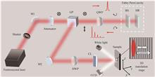
Laser-Induced Periodic Surface Structures (LIPSS) can be widely used in different processing fields, involving various materials such as semiconductors, dielectrics, metals, polymers. They have great potential in micro-nano processing. LIPSS are divided into two categories: Near-Subwavelength Ripples (NSRs) with period Λ larger than λ/2 and Deep-Subwavelength Ripples (DSRs) with period Λ smaller than λ/2, where λ is the incident laser wavelength. LIPSS can improve the surface properties of materials and can be used for modulation of the surface wettability of materials; enhanced surface Raman scattering; surface coloring; birefringence and optical storage, etc. They can be widely applied in many fields such as data storage, industrial manufacturing, and biomedicine.The formation of LIPSS is a complex process. Within a few nanoseconds after the femtosecond laser irradiation on the material surface, a series of ultrafast processes such as carrier excitation, carrier heating, lattice heating, plasma ejection, and nanoparticle ejection occur, which greatly increases the difficulty of processing regular NSRs. Therefore, how to improve the quality of NSRs has been an important research direction for femtosecond laser processing.Pulse shaping can regulate the distribution of laser energy in the time domain, which can then regulate the ultrafast process of laser-matter interaction. In order to fabricate high-quality LIPSS, we built a Fabry-Perot (F-P) cavity femtosecond laser pulse train processing system to conduct femtosecond laser time-domain shaping. The central wavelength of the laser is 1 030 nm, and we output femtosecond laser pulse train with flexible sub-pulse intervals in the range of 1~300 ps to fabricate NSRs on the silicon surface. The laser scanning velocity is altered by moving the sample through a 3D electronically controlled translation stage. By adjusting the distance between beam splitter and zero-degree mirror, we changed the sub-pulse interval and investigated NSRs induced by pulse trains with different sub-pulse intervals.After the samples were processed, we tested the surface morphology of the samples using a Scanning Electron Microscope (SEM). The NSRs induced by a Gaussian laser were slightly curved and had rough edges. However, the NSRs induced by the shaped pulse with a sub-pulse interval of 100 ps were uniformly oriented with smooth and straight edges. The peak of the spectrum obtained by its Fourier transform was (0.992±0.008) μm-1, corresponding to the period Λ=(1 008±8) nm. The laser fluence window of the NSRs induced by the shaped pulse with a sub-pulse interval of 100 ps was 0.08 J/cm2, which was four times as large as the NSRs induced by the Gaussian laser pulse. As the sub-pulse interval increased, regular NSRs could also be induced, but the width of single ripples was not uniform and the ripples started to become curved with inconsistent orientation. The surface morphology and depth of the sample were measured using a white light interference confocal microscope. The depth of regular NSRs induced by Gaussian laser pulse was (22±3.2) nm, and the depth fluctuation reached 14.4%. In contrast, the depth of regular NSRs induced by the pulse train of 100 ps was (45.7±2.7) nm, and the depth fluctuation was only 5.9%. The depth of NSRs induced by shaping pulse train was about twice that of the original Gaussian laser pulse. Meanwhile, the depth fluctuation was greatly reduced and the ripples were more regular. We used the ImageJ plug-in OrientationJ to measure the Divergence of Structure Orientation Angle (DSOA) of NSRs induced by Gaussian laser pulse and F-P cavity shaping pulses, and then analyzed the local orientation. The DSOA of the NSRs induced by Gaussian laser pulse was 7.9°, while the DSOA of the NSRs induced by pulse train of 100 ps was only 2.8°. The straightness and regularity of NSRs induced by all pulse trains were better than those induced by Gaussian laser pulse in the experimental range, which indicated that the NSRs induced by pulse trains were straight and regular. To quantitatively calculate the line edge roughness of the NSRs, we performed edge detection on the NSRs induced by different conditions. We obtained the one-dimensional straight line of the sample-averaged boundary by least-squares fitting and calculated the standard error of the line edge. The best NSRs induced by pulse train of 100 ps had an edge roughness of 3.9 nm, which could meet the standard of lithography process.In summary, NSRs induced by the femtosecond laser pulse train is superior to the NSRs induced by Gaussian laser pulse. The flatness, depth, and edge roughness of NSRs are significantly improved. Femtosecond laser pulse train can improve the quality of NSRs. Laser pulse shaping is expected to overcome the thermal effects, ejected particles and insufficient energy deposition during femtosecond laser processing and improve the processing accuracy.
Jul. 25, 2023Vol. 52 Issue 7 0752301 (2023)
Jiaxu HUANG, Jun LI, Pei QIU, and Shaolin XU
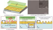
Laser-Induced Periodic Surface Structures (LIPSS) have been extensively studied as grating structures that form beyond the diffraction limit under laser irradiation over a large area. However, most LIPSS are essentially one-dimensional (1D) gratings, and this limited range of structural types in LIPSS hampers their widespread applications. To overcome this challenge, our study proposes a novel maskless two-dimensional (2D) laser nanopatterning method that combines the utilization of laser-induced thermal deformation effects and laser-Surface-Plasmon-Polaritons (SPPs) interference. By harnessing these two effects simultaneously, we can create two distinct periodic structures, namely wrinkles and LIPSS, in orthogonal directions. This innovative approach enables the generation of 2D wrinkled LIPSS on thin-film materials through a single-step laser irradiation process. Moreover, we have made significant advancements in the spatial modulation of the irradiated femtosecond laser, achieving a line shape with a length of 8 mm and a width of 7.78 μm. This spatial modulation facilitates efficient nanopatterning of these 2D LIPSS on a millimeter scale within seconds. These breakthroughs greatly expand the range of achievable structural types with LIPSS, making them more suitable for mass micro/nano fabrication. Our investigation focuses on the formation of wrinkles and LIPSS on Ge2Sb2Te5 (GST) thin-film materials, with an emphasis on laser-induced thermal accumulation, thermal deformation, and laser-SPPs interference. During the laser-induced thermal deformation, wrinkles spontaneously generate with a period of approximately 270 nm on a 50-nm-thick GST film over a silicon substrate. Importantly, these wrinkles maintain their stability in terms of their periods under laser irradiation with varying laser pulse energies. Furthermore, their periods can also be accurately controlled and predicted through a thermal deformation model, which has been validated on GST thin films with different thicknesses and substrate materials. Similarly, another periodic structure, namely LIPSS, can also spontaneously form due to the periodic ablation caused by laser-SPPs interference. The periods of LIPSS, measuring around 410 nm on the same 50-nm-thick GST film, can be modulated by adjusting parameters such as laser wavelength or incident angle. This independent modulation capability allows precise control over the periods of 2D wrinkled LIPSS in both orthogonal directions. Furthermore, we explore the morphological evolution of 2D wrinkled LIPSS and observe a gradual transition from excessive ablation and periodic structure generation to simple crystallization modification as the scanning speed increases or the laser pulse energy decreases. By manipulating the excitation intensity of laser-induced thermal effects and laser-SPPs interference through increasing the laser pulse energy under a fixed scanning speed, we can freely transform the generated periodic structures from wrinkled structures and 2D wrinkled LIPSS to 1D LIPSS. It is worth noting that the height of LIPSS can exceed 65 nm, while the corresponding wrinkle heights typically reach around 34 nm. Additionally, the orientation of 2D wrinkled LIPSS can be controlled by adjusting the polarization angle of the incident laser, adding another parameter to manipulate these structures. Moreover, we have discovered that 2D wrinkled LIPSS formed under different laser polarizations exhibit varying levels of uniformity. Comparatively, LIPSS display superior uniformity when compared to wrinkles, with their orientation being influenced by the polarization angle of the irradiated laser. The laser nanopatterning method proposed in this study demonstrates the immense potential for enhancing the diversity and expanding the applications of LIPSS. It not only overcomes the limitations associated with the monotonous structural type of 1D gratings in LIPSS but also offers a versatile means to engineer and customize the properties of thin-film materials. The increased range of structural possibilities and control over orientations pave the way for a great variety of applications, including surface modification, bionic structural coloration, high-precision detection, photonics, and optoelectronics. The findings presented in this study contribute to advancing laser nanopatterning techniques and provide valuable insights for future research in laser nanofabrication, a rapidly evolving field.
Jul. 25, 2023Vol. 52 Issue 7 0752302 (2023)
Liping SHI, Jiao GENG, and Min QIU
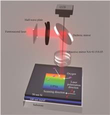
Laser-Induced Periodic Surface Structures (LIPSS) have emerged as a powerful tool in nanofabrication and nanophotonics due to their unique optical and surface properties. In recent years, the long-range uniformity of LIPSS formation have been a subject of extensive research, with efforts focused on optimizing laser parameters, material surfaces, and scanning strategies. In this study, we investigated the influence of scanning direction with respect to laser polarization on the regularity of LIPSS which was produced on metal/silicon hybrid thin films via femtosecond laser-induced surface oxidation.Our experimental findings revealed intriguing phenomena associated with LIPSS formation under different scanning directions relative to the laser polarization direction. When the scanning direction was perpendicular to the laser polarization, the nanometer-scale structures exhibited irregularities, such as branching and discontinuities. Conversely, when the scanning direction was parallel to the laser polarization, the structures demonstrated short-range order, but undesirable distortion occurred at the overlap of adjacent laser spots. Remarkably, when the scanning direction formed a certain angle with the laser polarization, long-range and uniform periodic nanostructures were readily obtained.To gain insights into the underlying mechanisms, Finite-Difference Time-Domain (FDTD)-based numerical simulations were conducted to elucidate the role of near-field enhancement and far-field interference during the laser-induced self-organization process. The simulations provided a comprehensive understanding of the interplay between the near-field and far-field effects, showing that near-field enhancements significantly impacted the spatial distribution of LIPSS. Consequently, we proposed an optimal scanning strategy that deviates from the conventional approach of perpendicular or parallel scanning relative to the laser polarization direction. By selecting an appropriate crossing angle between the scanning direction and the polarization direction, we effectively mitigated common issues like branching, discontinuities, and distortion, leading to the generation of high-quality and reproducible periodic nanostructures.Exploiting our new findings, we successfully fabricated one-dimensional periodic nanostructures on the surface of metal/silicon bilayer films by using single-beam femtosecond laser pulses. The quality and uniformity of the nanostructures were markedly improved by implementing the optimized scanning strategy. This breakthrough not only addresses the challenges associated with LIPSS formation but also opens up exciting opportunities for nanophotonics applications. The potential applications of periodic dielectric/semiconductor nanostructures on metal films in nanophotonics are vast and promising. These structures have demonstrated exceptional capabilities in refractive index sensing, nonlinear optical effects, photodetection, and structural coloring. Moreover, the low-cost and scalable nature of the proposed fabrication method offers great potential for widespread adoption in diverse applications.In conclusion, this research underscores the significance of optimizing scanning strategies for achieving high-quality and large-scale LIPSS. By considering the interplay of near-field and far-field effects during the self-organization process, we have demonstrated a novel approach to enhance the quality of LIPSS fabrication. Additionally, the applications of periodic nanostructures on metal films in nanophotonics hold promise for revolutionary advancements in various optical devices and technologies. The findings from this study lay the foundation for further exploration of LIPSS-based nanofabrication techniques, paving the way for a new era in nanophotonics and nanotechnology. Through continued research and innovation, LIPSS is poised to play a pivotal role in shaping the future of advanced nanophotonics and nanofabrication, impacting a wide range of scientific and technological domains.
Jul. 25, 2023Vol. 52 Issue 7 0752303 (2023)
Study on Polarization Dependence of Ultrafast Combination Pulse Ablation on Silicon Surface(Invited)
Huiqiang SHI, Qian YAO, Weiyi YIN, Zihuai SU, Jiang YU, Juan SONG, Xian LIN, and Ye DAI
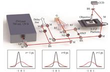
Since the invention of the laser, a great deal of research has focused on the mechanisms of laser-silicon interactions. Although ultrafast laser processing of Laser Induced Periodic Surface Structures (LIPSS) structures on silicon surfaces has been carried out for a long time, there are still problems, such as low processing efficiency in the preparation of large-area structures. The use of double pulse sequences has therefore been tried to improve the quality and efficiency of the process and has proved to be an effective strategy. A new method was provided for enhanced energy deposition by irradiating a ZnO surface with a Fs+Ps Double-Pulse Sequence (FPDPS) with a combined pulse width of 120 fs+2 ps and a sub-pulse energy ratio of 1∶1. On this basis, we investigate the nonlinear ionization dynamics causing the evolution of periodic structures by studying the effect of polarization angle, delay time and number of pulses between the double pulses on the area of the periodic structure, using an ultrafast combination double pulse with a repetition frequency of 1 kHz as an excitation tool on a silicon wafer with a crystalline surface of <100>. The experimental results show that under the combined pulse irradiation condition with a laser energy density of 0.23 J/cm2 and pulse combination of 100 pulses, there is a“V”shaped variation pattern at all delays within ±50 ps. The structure area induced by orthogonal polarization is the smallest, and the maximum area reduction rate is about 45% compared to that induced by other incident forms. This is due to the repeated modulation of the local field suppressing the reduction of the periodic structural edge ablation threshold. Specifically, the first pulse forms a LIPSS structure at the center and produces a local field modulated by polarization. When the two pulses are polarized in the same direction, subsequent pulses will gradually strengthen the initial local field, forming an elliptical distribution of stable local field strengths, which will effectively promote the growth of the LIPSS structure through a positive feedback mechanism. However, when the two pulses are polarized in different directions, the arrival of the second pulse will form a new local field and re-modulate the local field formed by the previous pulse, which will result in some energy dissipation and a reduction in the overall local field intensity, but the local field intensity at the center of the irradiation is theoretically almost unaffected, forming a circular local field intensity distribution when polarized orthogonally. Because the transient local field enhancement effect produced by laser irradiation promotes a lowering of the material ablation threshold, repeated changes in the local field not only inhibit the effect of the positive feedback mechanism, but also inhibit the effect of the local field enhancement in promoting a lowering of the ablation threshold. This effect is concentrated at the edges of the laser irradiated region, so we believe that the area of the LIPSS structure decreases with increasing polarization angle because the repeated changes in the local field suppress the reduction of the ablation threshold at the edge part of the LIPSS structure. At orthogonal polarization, the electron ionization to matter ejection can be characterized by observing the change in the area of the induced structure as the varied pulse delay times. According to the above theory, we designed experiments to test it. We used a 50× objective (NA=0.55) at a delay time of 2 ps. At an energy density of 0.19 J/cm2, differences in parallel and orthogonally polarized LIPSS morphology are observed, which is consistent with our theoretical interpretation. This combination pulse modulation technique provides a way for studying the polarization dependence and electron ionization efficiency of ultrafast laser-induced periodic structures on semiconductor surfaces, and further improvements are expected to enable the rapid fabrication of super-diffractive limit structures.
Jul. 25, 2023Vol. 52 Issue 7 0752304 (2023)
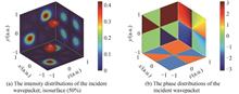
Dewei MO, Yongxi ZENG, Guoliang CHEN, Houan TENG, Jian CHEN, and Qiwen ZHAN
It is well known that photons not only carry linear momentum, but also have spin angular momentum related to polarization and Orbital Angular Momentum (OAM) linked with spiral phase. In addition, Spatiotemporal Optical Vortices (STOVs) carrying transverse OAM bring emerging research interests to the optical field. In this paper, we studied the characteristics of tightly focused scalar STOVs and the controllability of OAM orientation in the focused wavepacket. For an incident spatiotemporal wavepacket, which has three mutually orthogonal OAM, including two transverse OAMs and one longitudinal OAM, the corresponding focused wavepacket on the focal plane will collapse due to the spatiotemporal astigmatic effect of the high numerical aperture lens. Based on the modes conversion principle of the cylindrical lens, the incident spatiotemporal wavepacket is preconditioned. And the preconditioned spatiotemporal wavepacket will produce an intact focused wavepacket with a spiral phase in spatiotemporal plane. Debye integral is used to simulate and analyze the characteristics of tightly focused spatiotemporal wavepackets. The numerical simulation results of the preconditioned incident wavepacket show that it is split into two independent parts, the intensity is mainly distributed in the x-t plane and y-t plane, and both of these two planes exhibit binarized phase distributions. In the x-y plane, the phase abruptness caused by the preconditioning gives rise to discontinuous phase distribution in the range of [-π,π]. Here, the tightly focused spatiotemporal wavepackets carrying a single transverse OAM or a purely longitudinal OAM are also presented to facilitate the observation of the mutual coupling phenomena between different OAMs. The tightly focused wavepacket with a single OAM exhibits regular doughnut shape, while the three mutually orthogonal OAMs in the focused wavepacket will produce complex coupling phenomenon, leading to the focal wavepacket having an exotic phase singularity trace. Both the phase distributions on the x-t and y-t plane vary continuously from -π to π along the counterclockwise direction, indicating that the topological charge of the transverse OAM in these two planes is +1. In the x-y principle plane, five dark areas appear and each area corresponds to a phase singularity. In the central dark area, the phase varies continuously from -π to π along the clockwise direction, while in the other four dark areas, their phases vary continuously from -π to π along the counterclockwise direction. Thus, the OAM topological charge of the central vortex is -1 and the OAM topological charge of the four peripheral vortices is +1, which is caused by the spatiotemporal coupling. To further analyze the complex coupling phenomenon, the tightly focusing process can be regarded as a Fourier transform of the incident field.According to the expression of the incident field on the principle plan, it can be divided into three parts. The Fourier transformation of the first part will result in two pulse along the x-axis in the focal region, the Fourier transformation of second part will result in two pulse along the y-axis in the focal region, and the Fourier transformation of third parts will produce a highly confined vortex of topological charge of +1 in the focal region. Based on the principle of Fourier transformation, the Fourier transformation of the product of the above three terms is equal to the convolution of their respective Fourier transformations. The convolution of shifted pulse and highly confined vortex will result in the shift of the vortex. Thus, five phase singularities are generated by the complex coupling during the tightly focusing process. Meanwhile, to demonstrate the three-dimensional spatiotemporal evolution trajectory of the phase singularity, we extract the hollow structure inside the focused wavepacket. From the result, we find that the spatiotemporal coupling in the center of the focused wavepacket is stronger than in the peripheral region. We also calculate the topological charge of the OAM within different slices of the focused wavepacket to quantitatively analyze the effect of the spatiotemporal coupling on each kind of OAM. The numerical results show that, the spatiotemporal coupling has few effects on the longitudinal OAM of the focused wavepacket, which provides the possibility to control the focused wavepacket OAM orientation by adjusting the topological charge of the longitudinal OAM in the incident wavepacket. Different topological charge (l=-2,-1,0,1,2) of the longitudinal OAM in the incident wavepacket is taken, and the overall OAM of each tightly focused wavepacket is estimated. The results show that the overall transverse OAM of the tightly focused wavepacket is kept constant while the topological charge of the longitudinal OAM in the focused wavepacket reveals a linear relationship with the topological charge of the longitudinal OAM in the incident wavepacket. Hence, the overall OAM orientation of the focused wavepacket can be controlled by adjusting the topological charge of the longitudinal OAM in the incident wavepacket. Such tightly focused spatiotemporal wavepackets with controllable OAM orientation may find potential applications such as optical trapping, optical tweezer, spin-orbital coupling, micro-nano fabrication.
Jul. 25, 2023Vol. 52 Issue 7 0752305 (2023)
Jiaqi CUI, Xiaozhu XIE, Yajun HUANG, Zhaoyan LI, Yuhang LUO, and Jiangyou LONG
Nanosecond laser processing technology is widely used in Integrated Circuits (IC), optoelectronic devices, biology, medical, aerospace, and network technology due to its low cost, high precision, non-contact directional processing, and high efficiency. As the feature size of IC and Optoelectronics continues to decrease, copper (Cu) has become the mainstream interconnect material in electronic components, which has the advantages of low cost, low resistance, strong conductivity, high thermal conductivity and excellent ductility. Microcircuits prepared by narrow pulse laser induced selective ablation of Cu films on transparent substrates have attracted extensive attention from researchers because of their excellent optical and electrical properties. It has become a research hotspot in this field on how to obtain higher processing quality and efficiency, satisfy the processing requirements of various materials and structures. In recent years, the major processing method has been laser forward induced selective ablation of metal thin films to fabricate microstructures. However, this method inevitably produces heat-affected zones and nano-ripples during processing, this situation seriously reduces the quality and photoelectric properties of the metal film microstructure. In order to decrease the influence of laser thermal effect, avoid the accumulation of remelted material, and effectively improve the surface morphology and photoelectric properties of microstructure, this paper uses a narrow pulse width laser to selectively remove metal thin films and prepare microcircuits on the rear side. Firstly, the laser beam passes through the transparent substrate, and then irradiates the glass substrate and Cu film interface for laser selective induced ablation. Part of the Cu film in the ablation area is vaporized, and a huge pressure is generated in the closed space, thereby promoting the remaining metal film on the transparent substrate to be ejected. This unique ablation process has become an important preparation method for metal film microstructure owing to its high removal efficiency and high-quality processing effect. Based on the fabrication of microgrooves by nanosecond laser removing metal films, the effects of process parameters such as laser pulse energy and scanning speed on the front and rear side ablation of metal films by narrow pulse width laser (λ=532 nm, τ=1.8 ns) were investigated. By comparing the relationship between the groove width and the laser pulse energy at the same scanning speed, it can be concluded that the groove width increases with the enlargement of laser pulse energy on the front and rear side ablation. When the laser energy enlarges to a certain value, the groove width gradually reaches a certain level, and then remains stable. On the front side ablation, the width of the groove decreases with the increase of the scanning speed. At the same time, on the rear side ablation, the groove width is not sensitive to the scanning speed. As the scanning speed increases, the groove width does not change significantly. Since the width of the groove in the reverse removal is independent of the laser scanning speed, the edge shape of the groove can be improved by changing the laser scanning speed. By further optimizing the process parameters and analyzing the surface morphology of the microstructure in detail, it is proved that the performance of the microgrooves prepared by narrow pulse width laser (E=0.403 μJ, v=2 mm/s) on the rear side ablation is better than the front side. It not only has a straight and steep edge morphology, but has almost no sputtering on the edge. Through the experiments comparison of the front and reverse removal, it can be seen that the groove removed by the laser from the rear side is narrower than that removed from the front, which is impertinence of the variation of laser power. The difference in groove width between the two laser induced ablation methods could be attributed to diverse beam propagation and material removal processes. In addition, the 3D morphology of the microgrooves is characterized by a Confocal Laser Scan Microscope (CLSM), and the removal depth of the microgrooves is about 150 nm. This indicates that the Cu film on the glass substrate is completely removed and the glass substrate is not damaged which is crucial for the electronic isolation and photoelectric properties of actual electronic devices. In consequence, under the existing experimental conditions of our group, the microstructure of metal film prepared on rear side ablation has preferable quality. Combined with the temperature field simulation results of metal film by narrow pulse laser selective removal, the ablation mechanism and material removal mechanism of front and rear side ablation are revealed from the perspective of experiment and theory. To verify the feasibility of this removal method, uniformly distributed Cu arrays and complex microcircuit patterns are prepared when the laser energy is set to 0.403 μJ, and the scanning speed is 2 mm/s. The resistivity of the microcircuit measured by the double probe measuring instrument is 1.81 μΩ·cm, which is equivalence with the resistivity of the copper body. As a result, the microcircuit has excellent conductivity. Finally, the sample is placed in deionized water for ultrasonic 10 min, and the morphology of the microcircuit has no change. It proves the microcircuit processed by laser reverse processing has good adhesion and could be used for IC. Furthermore, this method has good application prospects.
Jul. 25, 2023Vol. 52 Issue 7 0752306 (2023)

Yang LIU, Xiangping ZHU, Chuan JIN, Xiaomo ZHANG, and Wei ZHAO
The “moth eye” micro-nano structure has recently attracted much attentions due to its high potential value in scientific, biomedical, and industrial applications. For example, by manufacturing specific micro-nanostructures on the surface of an optical device, the incident light would be reflected multiple times on its surface, which lets the surface achieve the co-called “light trap effect”, reducing the transmission loss caused by Fresnel reflection at the interface. Laser Induced Periodic Surface Structures (LIPSS) provide a robust, flexible, non-contact, simple, and low-cost potential method for the fabrication of large-scale surface micro-nanostructures. As the most frequently used material on optical devices, it is of great significance to study the fabrication of optical micro-nanostructures on fused silica surfaces.In this paper, by using Ti:sapphire femtosecond laser processing system, the general laws of femtosecond laser induced LIPSS morphology on fused silica samples have been studied. Through designed experiments, the effects of different laser fluence and repetition frequency, pulse number, spot size, and pulse spatial interval on the morphology of LIPSS on fused silica surface were studied. We also focus on how to obtain the high-quality LIPSS, which can have a great impact on the final performance of the device.Different fluences were first set in the experiments. It was found that at a laser fluence of 5 J/cm2, irregularly arranged nanospikes were densely distributed in the crater, and at 7 J/cm2, ripple-like structures appeared in the center of the crater. After that, as the laser fluence increased, the periodicity increased, accompanied by an increase in proportion. A laser surface plasma interference model is used to explain the relationship between periodicity and laser fluence, which is in good agreement with the observed phenomena.In order to investigate the effect of laser spot size (or the influence aera size of laser spot) on the morphology of LIPSS, diminished laser spot sizes were set to observe the changes. To further reduce the size of laser spot, the concept of threshold effect was adapted. The results show that by the reduction of laser spot size, the LIPSS stripe becomes more regular. A grating-like LIPSS with good quality can be obtained under the 1 μm diameter of laser spot when the laser fluence is set around 3.7 J/cm2.The effects of pulse number and laser repetition rate on LIPSS were also studied in this work. The results showed that only some defects could be observed on the surface when the pulse number was set to 1. As the pulse number increased, the ripple-like structures gradually appeared, but were irregular. When the pulse number was set to be 10, relatively intact fringes showed up. It is found that the periodicity of the fringes showed a decreasing trend with the increase of the pulse number. It is also found that changing the laser repetition rate alone has no significant impact on the morphology of LIPSS.Considering that laser fabrication is a line scanning process, there is a certain spatial distance between pulses. Therefore, we studied the effect of pulse spatial interval on the morphology of LIPSS. The results showed that when the spatial interval of pulses is similar to the periodicity that the LIPSS structure under current parameter conditions, high-quality, regular, long-range arrayed grating structures can be obtained. Specifically, we adopt the following parameters, 1 μm diameter of laser spot, a scanning speed of 20 μm/s, repetition rate 100 Hz, and laser fluence 4.2 J/cm2, and a highly regular long range aligned nanograting structure was fabricated, with a period of 200~300 nm and the depth of about 300 nm. The results found in this work may be conducive to promoting the development of surface micro-nano optical structures on fused silica.
Jul. 25, 2023Vol. 52 Issue 7 0752307 (2023)
Xing LUO, Ming LI, and Jianyong MAO
Zinc sulfide is a widely used infrared window material. Due to its high refractive index and strong surface Fresnel reflection, improving its anti reflection performance in the infrared band is of great significance. The traditional method to improve the antireflective performance is to prepare a film on the surface of zinc sulfide, but the antireflective film has the disadvantage of detachment and it is a limited antireflection effect on infrared signals with a wide spectrum and a large angle incidence. Preparing subwavelength structures on the surface of zinc sulfide can effectively improve its antireflective performance. This can be achieved by adjusting the microstructure parameters. Femtosecond laser processing has unique advantages of programmability and non-contact, making it a promising one-step manufacturing method for subwavelength microstructures. In this paper, the finite difference time-domain method is used to simulate the antireflection characteristics of the zinc sulfide surface structure, which is prepared by femtosecond laser processing, and then the infrared transmittance of the structure array surface is measured.This article is based on zinc sulfide material, simulating and preparing one-dimensional strip structure and two-dimensional grid structure and further testing the infrared transmittance of both structures. Firstly, FDTD software was used to simulate and calculate the infrared transmittance characteristics of the zinc sulfide surface structure.Determine the unit structural parameters of the structural array by simulating the height of the strip structure. On this basis, two types of structural arrays with different spacing were designed, and the simulation results showed that as the spacing between structures decreased, the transmittance increased. The trend exhibited by one-dimensional strip structures and two-dimensional grid structures is consistent. Secondly, two types of structural arrays were prepared using femtosecond laser processing. The test results indicate that as the spacing between the one-dimensional strip structures decreases, the transmittance tends to increase, which is similar to the trend shown by simulation. The two-dimensional grid structure with small spacing has higher roughness, so the structure array with 8 spacing has better transmittance. In actual processing, it is necessary to comprehensively consider the influence of surface roughness and ablation degree on the transmittance, and reduce the Fresnel scattering of light waves by edge cracks. Finally, the transmittance of the samples was tested in the range of 7~10 μm in the mid to far infrared bands. The structure array with a spacing of 5 μm increases the infrared transmittance by approximately 6% at wavelengths 9.5~10 μm. The grid structure with a spacing of 8 μm can increase the average transmittance by 4% in the 8.5~10 μm bands and nearly 7% at the 10 μm wavelengths. In addition, the transmittance spectrum measured in the experiment has good transmittance in the long wavelength range, which is related to the scattering effect of nanoscale structures generated by laser processing at different wavelengths, the surface scattering effect of non-uniform micro nano composite structures is more pronounced at shorter wavelengths. Compared with the simulation result, it was found that the overall transmittance of zinc sulfide decreased. The overall decrease in the transmittance of zinc sulfide samples is related to two factors: the first reason is the light absorption effect caused by structural defects in femtosecond laser processing, part of the light is absorbed by zinc sulfide, and the second reason is the diffraction and light scattering effects caused by non-uniform surface particulate matter generated by laser processing, which deflects the incident light along the beam transmission path. The experimental results indicate that the prepared structure has good anti-reflection performance, indicating that the method used in this paper has a positive effect on improving the transmittance of zinc sulfide. This provides a reference for studying the transmittance of zinc sulfide in the mid-infrared band.
Jul. 25, 2023Vol. 52 Issue 7 0752308 (2023)
Jian CHENG, Jiale LI, Zhiwei ZHANG, Sheng JIANG, Peng ZHANG, Zhongsheng ZHAI, and Dun LIU
Aramid Fiber Reinforced Plastics (AFRP) are with excellent physical properties, but defects such as burrs and damage may result from traditional mechanical drilling methods, whereas the potential to avoid these issues exists in laser drilling technology. However, thermal effects would induce severe thermal damage to AFRP components during the ablation process by continuous wave laser or nanosecond laser. It is suggested that ultra-short pulse width of ultrafast lasers can effectively suppress thermal diffusion. Accordingly, drilling experiments were conducted on one of the AFRP substrates, i.e., Kevlar-29 by using femtosecond laser in this study, aiming to improve the quality of laser drilling, reduce thermal damage and thermal influence zones during laser ablation, enhance the geometric accuracy of circular holes, and optimize the processing parameters of femtosecond laser drilling. The experimental material is a 2 mm thick Kevlar-29 fiber-reinforced composite, the laser focal plane is set at half the thickness of the material, and the designated hole diameter is 6 mm. The laser wavelength is 1 030 nm and the pulse width is 480 fs. Firstly, the drilling effect of two scanning strategies, cross-scan and concentric ring scan, was compared, and the scanning strategy with superior drilling effect was determined. Furthermore, the influence of laser processing parameters (laser power, laser repetition rate and laser scanning speed) on drilling quality was analyzed using orthogonal matrix experiments. Confocal microscopy and ultra-depth microscopy were used to observe the circular hole morphology after laser drilling, and the size of the thermal influence zone was measured. The effects of laser power, scanning speed, and repetition rate on circular hole morphology, thermal influence zone size, and geometric accuracy were analyzed. Finally, quasi-static tensile tests were conducted using a universal tensile testing machine, and the tensile strength of the samples after laser drilling was compared with those by using mechanical drilling processes. It has been found in this research that concentric ring scanning is more efficient than cross-scanning and the roundness of hole topography of concentric ring scanning is better. Within a certain femtosecond laser processing window, the overall size of the heat-affected zone will gradually increase as the laser power increases. Nevertheless, this increasing trend of heat-affected zone develops when the repetition rate is reduced, or the scanning speed is decreased. Moreover, a larger heat-affected zone and surface damage can also be produced if insufficient burning happens due to inadequate laser power. The optimal laser parameters for the heat-affected zone are a laser power of 5 W, a scanning speed of 1 050 mm/s, and a repetition rate of 200 kHz. The decrease in the taper angle of the femtosecond laser drilled hole is proportional to the laser power increasing and repetition rate decreasing. When the laser repetition rate is 200 kHz and the laser power reaches 9 W, a minimum taper angle of the hole is obtained as 6.99°, meantime a relatively large heat-affected zone is produced under these process parameters. It is found that the optimal taper angle of the hole is 14.10° with the least heat-affected zone. The tensile strength of the material after femtosecond laser processing is similar to that of traditional mechanical processing, but the fluctuation of tensile strength test performance is smaller. It has been indicated by the results that femtosecond laser drilling of Kevlar-29 fiber-reinforced composite is not a completely “cold” process, as thermal damage to the fibers and the surrounding matrix material is seen which is caused by the poor thermal conductivity of aramid fibers, hence resulting in the appearance of a relatively small heat-affected zone. To summarize, the use of appropriate laser parameters for femtosecond laser drilling of Kevlar-29 fiber-reinforced composite can effectively reduce the size of the heat-affected zone and improve the geometric accuracy of the hole so as to meet the requirements for precision and strength in related application fields.
Jul. 25, 2023Vol. 52 Issue 7 0752309 (2023)
Tao ZENG, Yuliang YI, and Lanjun GUO
When femtosecond laser beam power is much larger than the critical power for self-focusing, the beam breaks up into multiple filaments, which have appeared as a promising medium for multichannel white-light radiation, enhanced terahertz generation, enhanced air lasing, and waveguiding of microwave radiation. These applications rely on the realization of a high reproducibility and regular localization of multifilament array pattern. A four-petal Gaussian beam can evolve into a number of mirror symmetric petals in the far field and the petals of higher order beams can be equally spaced. Moreover, the space among the petals is determined by the beam order. Therefore, the four-petal Gaussian beam are a promising beam type for the generation and control of a regular multifilament array. In this study, the linear propagation of a four-petal Gaussian laser beam has been simulated based on Helmholtz wave propagation equation. The result shows that the four-petal Gaussian laser beam evolve into more petals in the far field. A 3×3 laser beam array is generated with beam waist of 0.5 mm and beam order of 2. Further, the spatial distribution of the laser filaments from a four-petal Gaussian femtosecond laser beam has been investigated based on the nonlinear wave propagation equation. When the total laser power of the four-petal Gaussian femtosecond laser beam is 32Pcr, a 2×2 regular multifilament array is generated finally. Here, Pcr is a critical laser power for self-focusing, which is a critical value for the formation of a laser filament. The waist radius and beam order of the four-petal laser beam are set to be 0.5 mm and 2 respectively. The separation between to closed filaments in the laser array would remain at 0.146 cm. If the beam order is set to be 5, the separation between to closed filaments would increase and remain at 0.23 cm. When the total laser power of the four-petal Gaussian femtosecond laser beam is 28Pcr, the waist radius and beam order of the four-petal laser beam are 0.5 mm and 2, the laser beam would split and emerge together during the self-focusing process, leading to a single laser filament occurrence finally. When the waist radius of the four-petal Gaussian femtosecond laser beam is 0.2 mm, the total laser power and beam order are 28Pcr and 2, a regular multifilament array is generated. The separation between two closed laser filaments is around 0.05 cm at the initial stage. Then the separation decreases versus the propagation distance and the multifilament array emerge into a single laser filament finally. The above results indicate that when the input power of a four-petal Gaussian femtosecond laser beam is relative strong, a regular multifilament array will be generated. At the source plane of the four-petal Gaussian laser beam, the separation of the four petals is directly proportional to both the square root of the beam order and the waist radius. Thus, the multifilament array space can be tuned by the initial beam waist and beam order. Generally, the size of the filament background energy reservoir is about 1 mm, which can influence the interaction between two closed filaments in the multifilament array. When the separation is larger than the size of the background energy reservoir, the multifilament array propagates stably and the separation remains constant. When the separation is less than the size of the background energy reservoir, the separation decreases versus propagation distance and the multifilament array evolves into a single filament finally. When the input power of the four-petal Gaussian femtosecond laser beam is relatively low and still larger than the critical power for self-focusing, the multiple self-focusing phenomenon will occur. The laser beam evolves into a single filament finally. This study has provided a new method for the generation of a regular multifilament array and could pave the way to some potential applications relying on multifilament arrays, such as enhanced terahertz generation, air lasing, and waveguiding.
Jul. 25, 2023Vol. 52 Issue 7 0752310 (2023)
Jian LIN, Yuxiao LIU, Qiang FU, Jun LI, Pengjun WANG, and Weiwei CHEN
To satisfy the ever-increasing bandwidth demands, silicon-based optical interconnects can offer a promising solution, thanks to the advantages of broad bandwidth, high speed, and excellent CMOS compatibility. Various advanced multiplexing technologies have been employed to further improve the transmission capacity, such as space division multiplexing, polarization division multiplexing, and wavelength division multiplexing. Among them, mode division multiplexing utilizing each mode to serve as an independent data channel has been drawing much attention. To construct the densely integrated mode division multiplexing system, multimode waveguide bends are one of the important functional components. Up to now, a number of structures, such as photonic crystal, multimode interference, and subwavelength grating, have been used to realize different multimode waveguide bends. Although these multimode waveguide bends can have good performance, they only support 2 to 4 modes and are not easy to expand. Thus, scalable multimode waveguide bends, which can support more modes, are highly desired. In this paper, a scalable multimode waveguide bend based on tapered couplers is presented. As an example, the multimode waveguide bend supporting TE0, TE1, TE2, TE3 and TE4 modes are designed and analyzed in detail. The proposed multimode waveguide bend is a symmetrical structure. It is composed of single-mode bend waveguides and a pair of five-mode multiplexer and demultiplexer. By utilizing the matching of the effective modal indexes, the mutual conversion between the fundamental mode and the high-order modes can be realized in each tapered coupling region, and thus multimode bending transmission is achieved. To improve the performance, the particle swarm optimization algorithm and finite difference time domain method are used to optimize the structural parameters of the tapered coupling region. Simulation results show that, for the designed multimode waveguide bend, within a bandwidth from 1 500 nm to 1 600 nm, when the TE0 mode is input, the insertion loss is smaller than 0.087 dB, and the crosstalk is less than-20.72 dB. As the TE1 mode is launched into the input port, the corresponding insertion loss and crosstalk are respectively lower than 0.27 dB and -19.81 dB. The corresponding insertion loss and crosstalk are less than 0.40 dB and -19.60 dB when the TE2 mode is injected into the input port. As the TE3 mode is input, the corresponding insertion loss and crosstalk are lower than 0.78 dB and -20.34 dB. When the TE4 mode is launched into the input port, the corresponding insertion loss and crosstalk are smaller than 0.75 dB and -19.03 dB. In order to verify the feasibility of our design, the optimized multimode waveguide bend is experimentally demonstrated on a silicon-on-insulator platform by using a commercial complementary metal-oxide-semiconductor compatible process. The experimental results reveal that, for the fabricated device, within a bandwidth from 1 520 nm to 1 600 nm, the insertion loss is lower than 1.71 dB, and the crosstalk is less than -10.60 dB when the TE0 mode is injected into the input port. When the TE1 mode is launched into the input port, the insertion loss and crosstalk are respectively lower than 3.04 dB and -11.35 dB. When the TE2 mode is input, the insertion loss is smaller than 2.9 dB, and the crosstalk is less than -10.92 dB. The corresponding insertion loss and crosstalk are smaller than 3.16 dB and -10.35 dB when the TE3 mode is injected into the input port. When the TE4 mode is input, the insertion loss is lower than 4.00 dB and the crosstalk is less than -11.45 dB. The main reasons for the inconsistency between the experimental results and the simulation ones are as follows: firstly, the scattering loss can be induced by the sidewall roughness of the fabricated waveguide. Secondly, due to fabrication errors, the actual width of the fabricated waveguide could deviate from the optimal value, so that the insertion loss and crosstalk of the fabricated device would become worse. Thirdly, owing to the bandwidth limitation of the adopted light source, the measured bandwidth is not as wide as the simulated one. In future work, high-quality fabrication processes are required to further improve the crosstalk and insertion loss. To sum up, with the above characteristics, our presented scalable multimode waveguide bend based on tapered couplers can offer an attractive option for constructing the densely integrated mode division multiplexing system to improve the transmission capacity.
Jul. 25, 2023Vol. 52 Issue 7 0713001 (2023)
Cairong GUO, Ruicheng JIANG, Dawei ZHANG, Shijie LIU, and Chunxian TAO
Magnetic fluids are widely used in the field of optical fiber magnetic field sensing as magnetic sensitive materials due to the adjustable refractive index. Optical fiber magnetic field sensor based on magnetic fluid has the advantages of high sensitivity and light weight, but the magnetic field measurement range of this kind of sensor is affected by the saturation magnetization of magnetic fluid, which limits the high magnetic field sensing range. Some studies have shown that magnetic hydrogels have the characteristics of high sensitivity to magnetic field, high saturation magnetization, high magnetic responsiveness and super magnetic similarity with magnetic fluids. In this paper, it is proposed to replace the base liquid of magnetic nanoparticles of magnetic fluid with hydrogel material to prepare magnetic hydrogel, hoping to seek a higher level of saturation magnetization, and make prospects for further improving the magnetic field measurement range of optical fiber sensors. A polyvinyl alcohol/ferric oxide (PVA/Fe3O4) magnetic hydrogel was prepared by the composite method, and used a fiber end face reflection-based measurement method to test the refractive index variation of the magnetic hydrogel under different magnetic fields, which proved that it had magnetic-induced refractive index variation characteristics and could be applied in the fiber magnetic field sensing structure based on refractive index variation. Based on this research, a cone-shaped fiber sensing structure based on magnetic hydrogel was designed. Single-mode optical fiber is pulled into a cone shape by melting and pulling method, and magnetic hydrogel is wrapped in the cone area and waist area of the cone-shaped optical fiber. The input light in the fiber will generate evanescent wave when it is in the conical transition region, which will excite the higher-order cladding mode in the fiber. After the fundamental mode and cladding mode are transmitted in the waist region of the tapered fiber, mode coupling and mode interference will occur when entering another tapered region. When the intensity of the magnetic field applied in the external environment changes, the refractive index of the magnetic hydrogel will change. In this experiment, we change the refractive index of the magnetic hydrogel by applying magnetic fields of different intensities to the sensing element of the tapered fiber wrapped by the magnetic hydrogel. The spectral change of the output light of the tapered fiber is detected by using the evanescent wave in the tapered region of the tapered fiber, which is sensitive to the refractive index of the external environment, to study the magnetic field sensing characteristics of this structure. The experimental results show that the sensitivity of wavelength shift is 86.42 pm/mT within the range of 6.4~22.6 mT, when the magnetic particle concentration is 2.1% at a constant temperature of 22 ℃. And also the sensitivity of wavelength shift is 51.42 pm/mT within the range of 5.5~30 mT, when the magnetic particle concentration is 2.9%. From the point of view of optical fiber magnetic sensing measurement, magnetic hydrogel has high application value and deserves further research. This paper also proposes that the detection sensitivity can be improved by selecting more appropriate dispersants to improve the dispersion uniformity of magnetic nanoparticles in hydrogels, and by improving the structure of optical fiber sensing elements. During the preparation of magnetic hydrogel, we can further improve the magnetic field sensing range and expand the application of magnetic hydrogel in the field of optical fiber magnetic field sensing by optimizing the freezing and thawing times and the concentration of magnetic nanoparticles.
Jul. 25, 2023Vol. 52 Issue 7 0706001 (2023)
Licui SHEN, Sujuan HUANG, Wei CHEN, Cheng YAN, and Xinpeng ZHAO
Using different cores of a Multi-Core Fiber (MCF) as independent parallel spatial paths to transmit different information simultaneously offers cost, space and energy savings. The inter-core Differential Group Delay (DGD) is a key parameter of the multi-core fibers, and its accurate measurement is of great importance. In the multi-core fibers, errors in the preparation process or bending of the fiber caused by external forces can result in inter-core differential group delay in various cores. When light is transmitted in a multi-core fiber, the outgoing light from different cores will interfere with coherent superposition in space due to different group delays. According to this character, this paper proposes a spatial interferometric imaging-based method for measuring the inter-core differential group delay of multi-core fibers, and building an experimental measurement device. At the input of the multi-core fiber, the laser is shifted and injected by adjusting the three-dimensional adjustment table to excite different cores, and the output light of the excited cores will interfere in space. The computer controls the CCD to scan the wavelength of the input light in one dimension and records the spatial interferogram at different wavelengths in real time. The interferometric information of all pixels in the interferogram is used to construct a three-dimensional spatial interferometric spectrum, and the inter-core differential group delay of the multi-core fiber can be obtained by spectral analysis of the interferometric spectrum. The inter-core differential group delay of the weakly linked trench assisted seven core fiber is measured in this paper. We measured the inter-core differential group delay between the central and six outer cores respectively. When two cores are excited at the same time, a peak will appear at the delay difference between the two cores through the Fourier transform of the interference information. Subtracting the-inter core differential group delay between the central core and two adjacent outer cores yields the inter-core differential group delay between the two outer cores, which is only 10-4 dissimilar from the actually measured inter-core differential group delay of two adjacent outer cores. When three spikes are excited simultaneously, two adjacent spikes will interfere with each other. By Fourier transforming the interference information obtained by CCD containing the differential group delay, a plot of differential group delay versus interference intensity containing three spikes can be constructed. The values of the horizontal coordinates of the three spikes in the plot are the differential group delay between the three cores, and they correspond to the measurement results when only any two of the three cores are excited, respectively. Simultaneously, the bending dependence of the inter-core DGD of the multi-core iber is measured and researched. The inter-core differential group delay was measured for three bending radii of 5 mm, 75 mm, and 110 mm. The results reveal that the inter-core DGD decreases as the bending radius increases, which is consistent with the theory. This method's measurement instrument is simple, and the measuring precision can reach 10-4. It can measure the delay difference not only between two cores, but also between any nearby cores at the same time. In addition, the outgoing light from the end face of the multi-core fiber to be measured is focused through the objective lens and connected to the CCD and adjust the three-dimensional adjustment table, the excitation state of the cores in the multi-core fiber and the degree of coupling of optical energy can be observed on the CCD, which makes the selection and excitation of the cores to be measured easier. The spatial interference imaging approach suggested in this study has the characteristics of simple, fast, high accuracy. It can be widely used to measure inter-core DGD of the multi-core fiber in SDM systems, MWP signal processing and other application circumstances.
Jul. 25, 2023Vol. 52 Issue 7 0706002 (2023)
Hua QI, Yan FENG, Ruizhi PAN, Maomao XU, Haoxiang WANG, Hongpu ZHANG, and Hua ZHANG
With the further development of intelligent robots, bionic touch sensing has become an important means for the robotic dexterous hand to interact with the external environment, making it a hot topic. However, in the existing research on tactile perception of robotic hands, most of the sensing units have complex structures and are difficult to integrate in the hand.For touch sensing of the dexterous robot hand, this work employs optical Fiber Bragg Grating (FBG) as the information transmission and sensing carrier and develops a wearable touch fingerstall. The thumb fingerstall contains two segments: fingertip and finger pulp. The fingertip is composed of a curved surface and a plane surface. The curved surface can fit the thumb shape better, and the plane surface can provide a more stable touch. Specially, we use a cylindrical pin as the knuckle to connect the fingertip and finger pulp. The touch sensing of three contact positions of the fingerstall have been studied:position 1 is the vertical fingertip, position 2 is the 15° fingertip, and position 3 is the 30° finger pulp. Firstly, the fingerstall model was simulated using the finite element method to verify its structural feasibility. Then, the fingerstall was loaded using an electronic tension machine, ranging from 0 N to 10 N with a 1 N increment, and each load was held for 25 s. For each test position, the experiment was repeated three times, and the responses of FBG were recorded. Analysis of the touch sensing experimental data shows that the sensing fingerstall has good sensitivity and linearity within the 0~10 N touch pressure range. The average sensitivities at position 1, position 2, and position 3 are 24.119 6 pm/N, 10.338 3 pm/N, and -1.580 7 pm/N, respectively, with linearity above 99%. Overall, the simulation results are basically consistent with the experimental results, although some errors may arise due to 3D printing and FBG packaging. Therefore, different loading positions and forces can be distinguished by different center wavelength offset and offset direction of FBG.In order to verify the sensing performance of the fingerstall further, a hardness discrimination experiment was carried out primarily focused on perceiving objects of small hardness. And the standard ratio of wavelength to touch depth (ks) was proposed as a quantitative measure of hardness perception. Position 1 was selected as the experimental position for hardness perception, and four silicone blocks with different hardness (named as 0 HA, 10 HA, 20 HA and 40 HA) were selected as the experimental objects. Considering the time and safety factors, 5 mm was selected as the touching depth, and 60mm/min as the touching speed. The average responses of FBG to 0 HA, 10 HA, 20 HA and 40 HA are 58.57 pm, 242.3 pm, 580.95 pm, 1107.6 pm, respectively. The corresponding ks values are 11.717 pm/mm, 48.46 pm/mm, 116.19 pm/mm and 221.52 pm/mm, respectively. According to the data results, when the fingerstall touches the 40° silicone block, the ks is the largest, and the ks is the smallest at the 0° silicone block. When ks is larger, the greater the hardness of the object is. The sensing fingerstall has a good repetition, with repeatability errors of 3.82%, 0.97%, 0.51%, and 0.29%.In conclusion, a simple and wearable fingerstall has been designed. The tactile sensitivity of three different position has been studied, and a hardness discrimination experiment has been conducted. These research results can serve as a basis for bionic touch sensing of dexterous robotic hands.
Jul. 25, 2023Vol. 52 Issue 7 0706003 (2023)
Kaisheng ZHANG, Xiuqin SU, and Kai LIU
Star sensors are high-precision space attitude measurement devices used in astronomical navigation to obtain the attitude of space vehicles by observing the angular distance of stars. As a key technical parameter of star simulators, the angular distance between stars is an important indicator of their testing accuracy. It represents the angular position relationship between any two-star points, and its size depends on the position of each star point. As an important component of a star simulator, optical systems can cause changes in star position due to coma, field curvature, astigmatism, and distortion. These changes can lead to discrepancies between the calculated inter-star angular distance and the theoretical inter-star angular distance, thereby affecting the accuracy of the simulation. Therefore, studying the impact of optical system aberrations on the inter-star angular distance is an important guarantee for ensuring the high accuracy of the star simulator. In order to effectively improve the accuracy of the star simulator, this paper addresses the issue that the conventional mathematical formula for calculating the inter-star angular distance does not account for the impact of aberrations in optical systems. As a solution, a method for correcting the inter-star angular distance based on aberration influence is proposed in this study. The method involves establishing a relevant mathematical model and deriving the corresponding mathematical formula. Then, taking the star simulator platform of spherical screen projection as an example, analysis and experimental testing were conducted. The test results showed the following maximum impacts of various aberrations on the inter-star angular distance: -10.04″ for coma aberration, -13.07″ for field curvature, -2.92″ for astigmatism, and 34.78″ for distortion. Considering the compensation of each aberration on inter-star angular distance, the maximum total error of the influence of aberration on inter-satellite angular distance is 16.53″. Combining the established mathematical model of inter-satellite angular distance, curve fitting is performed on the azimuth and elevation angles of each star point to obtain a fitting curve for the position error of the star point affected by aberration, thereby completing inter-satellite angular distance correction. The experimental results show that the inter-satellite angular distance error before correction is 27.56″, and the inter-satellite angular distance error after correction is 16.96″, which is reduced by 10.60″ compared to the before correction. The research and experimental verification of inter-satellite angular distance correction methods for aberration effects provide a theoretical basis for effectively improving the simulation accuracy of satellite simulators.
Jul. 25, 2023Vol. 52 Issue 7 0712001 (2023)
Jiali PENG, Ping RUAN, Youjin XIE, Zhiguo LI, Jiahao WANG, and Jingyu HAN
The space electro-optical tracking and pointing turntable is a kind of space photoelectric payload, which is used to realize the stability of the optical axis and the tracking of the target in the space environment. In the process of launching, the turntable must endure many harsh mechanical environments such as vibration and shock, therefore, its dynamic characteristics directly determine the reliability of the turntable. When we use finite element method to analyze the dynamic characteristics, a finite element model that can accurately reflect the stiffness and damping characteristics of the turntable is the key to the analysis. The stiffness of the connected parts in the turntable, such as bearings and locking devices, has a great influence on the stiffness characteristics of the overall structure. In the current research, there is a distortion problem in the finite element modeling of bearings and locking devices.Aiming at this problem, this paper proposes an equivalent modeling method for bearing and locking devices by using generalized spring elements (bushing), which represents the behavior of a flexible connection or joint that allows translational and rotational movement. The translational degrees of freedom allow movement along the X, Y, and Z axes, representing the linear displacements in those directions, the rotational degrees of freedom allow rotation around the X, Y, and Z axes. We analyze the bearings and locking devices under dynamic load, establish their mechanical models, and define the significance of the Bushing elements stiffness matrix parameters.Then we simplify the structure of turntable, complete the equivalent modeling for shafting and locking devices by using Bushing elements, establish the finite element model of the turntable. Afterwards, we calculate a partial of bearing stiffness parameters based on Hertz contact theory. The remaining bearing stiffness parameters and all locking devices stiffness parameters that can not be theoretically calculated are obtained by parameter identification based on modal test data. Due to the stiffness of the bearings and locking devices decoupled from each other, we set up three different working conditions of modal test to obtain them. We use condition 1 (all locking devices: unlocked) to obtain the stiffness parameters of azimuth shafting and pitching shafting, condition 2 (azimuth locking devices: unlocked; pitching locking device: locked) to obtain the stiffness parameters of pitching locking device, and condition 3 (all locking devices: locked) to obtain the stiffness parameters of azimuth locking devices. Based on the obtained stiffness parameters, modal analysis is performed, the maximum relative error in natural frequencies between simulation and test is 5.1%, within the allowable margin. Finally, since the damping in the turntable system is a frequency-dependent damping, the constant damping used in traditional finite element analysis does not reflect real damping characteristics, we define damping characteristics of turntable by using modal damping. Modal damping is a frequency-dependent type of damping in finite element analysis, and suppresses responses by defining damping to each mode shape. Because of the superposition principle of damping effect, we use the maximum response of the X, Y, and Z directions in the 0.2 g swept-sine vibration test to identification the modal damping based on the constant damping of 0.02. Based on the obtained modal damping, harmonic response analysis is performed, the maximum relative error in the maximum responses of the X, Y, and Z directions between simulation and test is 3.2%, within the allowable margin. Hence the stiffness and damping parameters analysis of turntable is accurate, and the dynamic characteristics analysis is accurate.The results show that the method of using Bushing elements to model the bearing and locking devices equivalently can reflect the dynamic characteristics of the turntable more accurately than traditional modeling methods, and the methods of obtaining the stiffness and damping characteristics through theoretical calculation and parameter identification are feasible. It has a certain reference effect on the modeling and simulation of the same type of turntable.
Jul. 25, 2023Vol. 52 Issue 7 0712002 (2023)
Xueshun SHI, Xingang ZHUANG, Guoquan WANG, Hongbo LIU, Pengju ZHANG, Changming LIU, and Jinge ZHOU
Optical radiation measurement generally refers to the use of basic measurement technology to establish a direct or indirect connection between the measured optical radiation or photometric parameters and the fundamental physical constants or physical quantities with low measurement uncertainty, so as to improve the reproducibility or measurement level. In the actual substitution process, in order to ensure the measurement accuracy, the factors affecting the equivalent substitution of photoelectric heating need to be corrected. At present, most relevant studies at home and abroad only test and simulate the factors affecting the equivalent substitution of photoelectric heating of cryogenic radiometer from a single aspect, and the technical means adopted have some defects. The 41st Research Institute of China Electrics Technology Group Corporation has developed cryogenic radiometers. In order to ensure the measurement accuracy of cryogenic radiometer, the research on the optical power correction factor of cryogenic radiometer is carried out. The optical path structure of the cryogenic radiometer test system and the measurement process of optical power are introduced. The four main factors affecting the equivalent substitution of photoelectric heating of cryogenic radiometer were analyzed. Brewster window transmittance, stray light, absorbing cavity absorptivity and photoelectric heating non-equivalence are considered to be important sources of uncertainty of cryogenic radiometer. Brewster window transmittance, stray light and blackbody cavity absorption the three influencing factors were tested by using the influencing factor test facility, and the photoelectric heating non-equivalence factor is simulated and calculated by finite element analysis. Aiming at the transmittance and stray light correction factor of Brewster window, the beam alignment and test chamber are used for on-line measurement.With the test chamber, the stray light radiation is indirectly calculated by testing the transmittance of the incident light through the off-axis parabolic mirror, which is similar to the transmittance test of the Brewster window. The ratio of the power of the front and the rear of the parabolic mirror is the stray light correction factor. Because through hole diameter of the parabolic mirror is smaller than the blackbody cavity diameter, all the light that does not pass through the through hole is regarded as stray light, and all the light that passes through the through hole will enter the absorption cavity. At the same time, the Gaussian beam energy distribution after spatial filtering is analyzed. It is proposed to obtain the stray light distribution and energy by measuring the transmittance of incident light through off-axis parabolic mirror. Finally, the transmittance of Brewster window is 0.996 817, stray light correction factor 0.999 013. In addition, the spectral absorptivity of the black body cavity is analyzed and tested, and the factors affecting the absorptivity of the black body cavity are analyzed. The simulated and measured results are consistent. The absorptivity of the black body cavity at 632.8 nm is 0.999 950. Additionally, the heat transfer model of blackbody cavity is constructed by finite element analysis method. Firstly, the three-dimensional mathematical model of blackbody cavity assembly is constructed by SolidWorks, and the thermodynamic characteristic parameters of materials at temperature of 6.5 K are added, and then the established mathematical model is imported into SolidWorks simulation for thermodynamic simulation. The heating power, between 100 μW to 1 mW, stepped 100 μW, is applied to the light heating area and the electric heating area, respectively. The photoelectric heating non-equivalence of cryogenic radiometer under different heating power is simulated and analyzed. The simulation results show that the difference of photoelectric heating non-equivalence of cryogenic radiometer under different heating power is slight, and the photoelectric non-equivalence factor of the cryogenic radiometer is 1.009 240±0.000 010. The research results provide certain references for the optimization design and correction factor test of each functional module of cryogenic radiometer.
Jul. 25, 2023Vol. 52 Issue 7 0712003 (2023)
Yanna ZHANG, Fuxiang GUO, Wei WEI, and Xin LI
High-frequency radiometric calibration can track and correct the on-orbit state of the remote sensors in time to ensure the accuracy of observation data. In order to improve the accuracy and data consistency between the different remote sensors, the radiometric benchmark satellites have been developed in recent years. However, during the radiometric transmission of the radiometric benchmark satellite, due to the different orbits between the benchmark satellite and the remote sensor to be calibrated, the observation angles between the satellites are quite different, so the calibration frequency is limited under the condition of Simultaneously Nadir Observation (SNO) cross calibration. In order to improve the calibration frequency and reduce the impact of angle matching on calibration accuracy, a cross calibration method based on the multi-angle apparent reflectance model is proposed in this paper. The multi-angle apparent reflectance model of the stable target site is constructed to carry out the cross calibration of the benchmark satellite. The stable site used for the cross calibration is selected, and the multi-angle model of the site is constructed by grouping the observation angles, solar angles, and apparent reflectance of Terra/MODIS and AQUA/MODIS for 11 years from 2008 to 2019 under the multi-angle and high-precision remote sensors. The multi-angle model is suitable for the large angle cross calibration in the range of 0°~60° zenith angle. Based on the pseudo-invariance property of the stable site, the spectral matching function suitable for 400~2 400 nm band is constructed by using the average spectral apparent reflectance data of Hyperion, ignoring the variation of the time-dimensional. In the process of the benchmark satellite cross calibration, regional matching, time matching, and cloud removal are carried out for the reference sensor and the sensor to be calibrated at first. Then, the apparent reflectance measured by the reference sensor and the sensor to be calibrated is obtained using the model to complete angle matching and spectral matching. Finally, the calibration coefficients are calculated by combining the DN value of the sensor to be calibrated. According to the calibration principle in this paper, a multi-angle apparent reflectance model of the pseudo-invariance field Libya 4, which is recommended by CEOS, was constructed. Using AQUA/MODIS as the benchmark sensor, 205 times cross-calibration applications were performed on MERSI II of the Fengyun-3D satellite at six solar reflection bands from 2019 to 2020. The calibration coefficient and in-orbit variation trend of FY3D/MERSI II high frequency were obtained. In order to verify the accuracy of the cross calibration method in this study, 26 times a comparison of results was compared with SNO cross calibration method with strict angle limitation. The two methods have good consistency in the measurement trend. Compared with SNO cross calibration method, the calibration frequency increased from 26 times to 205 times, and the average relative deviation was less than 2.1%, which proved that the multi-angle hyperspectral apparent reflectance model constructed in this study could be better applied to cross calibration under the condition of large angle difference. The apparent reflectance model of the stable site is constructed by using the long-sequence, multi-angle and hyperspectral high-precision satellite data. The apparent reflectance model is suitable for the multi-angle cross calibration of the remote sensors within 60° observation angle and observation band within 400~2 400 nm. The calibration method in this study can solve the dependence on the multi-angle ground site data from the manual measurement, significantly improve the calibration frequency of the multi-type satellites. The calibration method timely track and correct the variation trend of load in orbit, and improve the quality of remote sensing data. However, the accuracy of the single point calibration and the seasonal fluctuations need to be further analyzed and improved. Through the application and comparison verification of more stable sites and more remote sensors, this method will promote the application of the multi-satellite quantitative remote sensing.
Jul. 25, 2023Vol. 52 Issue 7 0712004 (2023)
Yong ZHAO, and Yueming ZHOU
When atoms are exposed to strong femtosecond laser fields, there is a high probability that the electrons in atoms can be excited to the Rydberg states with very high principal quantum numbers and large orbitals, in addition to processes such as multiphoton ionization and tunneling ionization. This highly excited state of the atom is very stable in the ultrashort strong laser pulse and is closely related to many other phenomena in the strong field, such as neutral particle acceleration, multiphoton Rabi oscillations, near-threshold harmonic radiation. It has become one of the research hotspots in the field of strong-field ultrafast physics in the last decade. Among these studies, the mechanism of the generation of Rydberg atoms in strong laser fields, the modulation of Rydberg states by lasers, and the strong-field ionization process and stability of Rydberg states are the main issues of interest.This review provided an overview of the generation mechanisms of the Rydberg states driven by strong laser fields. There are two mechanisms for strong field Rydberg state excitation. One is multiphoton resonance excitation and the other is Frustrated Tunneling Ionization (FTI) excitation. The dependence of the yield of the Rydberg state atoms on the laser ellipticity is usually considered to be an important basis for determining whether the Rydberg state atom generation mechanism is multiphoton resonance excitation or frustrated tunneling ionization. However, this judgment is not reliable. As shown in this review, for multiphoton resonance excitation, the yield of Rydberg state atoms also decreases rapidly with increasing laser ellipticity. In contrast, in the nonadiabatic tunneling ionization region, the yield of Rydberg state atoms in FTI does not always decrease with increasing laser ellipticity, instead, it shows an abnormal increase in the yield. There is no clear boundary between these two mechanisms.This review focused on a variety of interference phenomena during the Rydberg-state excitation of atoms driven by strong laser fields, which are manifested as oscillations of the Rydberg state atomic yield with laser intensity. These interference phenomena are classified into three categories according to the magnitude of the as-Stark shift corresponding to the laser intensity interval of the oscillation period. The first category is the interference with an oscillation period of one photon energy. In multiphoton resonance excitation images, this interference can be understood as channel closing. In tunneling images, it can be understood as coherent recapture, wherein the electrons tunneling ionize at different laser cycles, are recaptured, and interfere, giving rising to the laser-intensity-dependent oscillation of the excitation yield. The second category is the interference with oscillation periods much larger than one photon energy, which usually appears in the long wavelength region. This type of oscillation is explained as the interference of the tunneling electron recaptured at different returns. The third category is the interference with oscillation period much smaller than one photon energy, due to the interference of the excitation during the rising and falling edges of the laser pulse, i.e., the dynamic interference. These interference phenomena provide the dynamic information of the strong-field excitation process of the Rydberg-state atom.In this review, the ionization processes of excited atoms in strong laser fields are also presented, in particular, the circular dichroism of ionization of the Rydberg atoms driven by circularly polarized laser fields. Because of this circular dichroism, the Rydberg state can be considered as the simplest chiral system, which is important for one to explore the chirality of molecules. In addition, the circular dichroism of Rydberg state atoms is also important for the preparing and detecting high-purity single ring current states at ultrafast time scales and the generation of spin-polarized electron pulses.
Jul. 25, 2023Vol. 52 Issue 7 0732001 (2023)
Yue YU, Haoxuan SI, Zuhua YANG, Shengzhen YI, and Zhanshan WANG
X-ray optics and systems have been widely used for applications such as plasma diagnostics, X-ray spectroscopy, astronomical observation and material analysis. The spectral characteristics of the optics and systems need to be accurately measured, for which a high-brightness monochromatic X-ray source is indispensable. Synchrotron radiation facilities provide the most reliable metrology, but their measurement timeliness is limited because of the allocated user beam time and long distances to reach the facilities. Commercial X-ray measurement equipment, such as X-ray fluorescence spectrometers, X-ray reflectometers and diffractometers, are only capable of measurements of small-size optics at a few fixed energy points. Desktop monochromatic X-ray sources that combine X-ray tubes with dispersive optics have provided a laboratory-based approach to calibrating X-ray optics, where the dispersive optics usually refers to multilayers, gratings and crystals. Multilayers are distinguished by their high luminous flux and wide working energy band, but their spectral resolution is relatively low; X-ray gratings allow for much higher spectral resolution, but the fabrication processes are quite difficult for extremely dense grooves for X-ray diffraction. Crystals have a naturally unique dispersion capability in the X-ray band that can substantially improve the spectral resolution. Common-used planar and cylindrical crystals have limited effects to enhance the system throughput because of relatively weak focusing capability in one or both dimensions; complex aspheric bent-crystals, such as toroidal, parabolic and hyperbolic crystals, can reduce aberrations and focus in both meridional and sagittal directions so that system throughput and spectral resolution can be significantly improved. However, aspheric bent-crystals are difficult to fabricate and have many limitations for application; and the aberration would deteriorate abruptly if the incident angle deviates from the designed value. Spherically bent-crystals enable two-dimensional focusing and are relatively easy to be fabricated; therefore, they have been widely used in X-ray spectrometers. Conventional spherical bend-crystal spectrometers adopt the Johann scheme, where the light source and the image plane are located on a Rowland circle with a diameter equaling to the radius of the concave bend-crystal. By applying Johann scheme, better focusing and higher spectral resolution are obtained in the meridional direction, but the brightness of the spectral lines acquired in the image plane is largely decreased due to light divergence in the sagittal direction. Therefore, it is necessary to optimize the optical structure to improve the intensity of dispersed monochromatic X-ray. In this paper, a desktop method for obtaining high-brightness monochromatic X-ray is proposed based on a spherical bent-crystal focusing structure. It achieves monochromaticity in the meridional direction using crystal dispersion, and obtains high brightness in the sagittal direction simultaneously based on spherical-mirror focusing. A geometric model is developed to theoretically compare the efficiency of collecting light of the spherical and cylindrical bent-crystals; also, the dispersion and focusing performance of different optical layouts with spherical and cylindrical bent-crystals are simulated and evaluated. Both theoretical and simulation results show that the spherical bent-crystal focusing structure has an excellent performance in terms of focusing characteristics, with the brightness of the spectral line obviously increased, compared with the cylindrical bent-crystal. In view of the monochromatizing requirements of the Al Kα1 line, a device based on low-power Al-target X-ray tube is designed and adjusted, and its performance was tested by spectroscopic experiments. Measurement results show that with the X-ray tube working at 7 W power and CCD exposure for 10 minutes, the count of the full-field spectrum of the Al Kα1 line is greater than 2×10⁵ with a spectral broadening of about 0.592 eV; when introducing a 200 μm beam-limiting slit, the spectral broadening is further reduced to 0.493 eV and the CCD count is about 2×10⁴. The results have verified that the device can effectively obtain the high-brightness Al Kα1 line, and also provides a new technical approach for accurately measuring the spectral characteristics of X-ray optics and systems.
Jul. 25, 2023Vol. 52 Issue 7 0734001 (2023)
Song NI, Jie CHEN, Haijun YU, Xiaojiao DUAN, Dabing CHEN, and Jianjun LIU
Cross-linked Polyethylene (XLPE) cable is widely used in urban power supply systems because of its excellent performance. Its inner structure-the water-blocking buffer layer-is prone to suffer from ablation defects after a long time of working, which will threaten the safety of the city's power supply. Therefore, the accurate detection of such cable defects is an urgent problem to be solved. In our previous work, we proposed a Local Source-translation Computed Tomography (L-STCT) method for cable detection. This method focuses on scanning part of the cable around the water-blocking buffer layer, and can intuitively observe the internal structure and identify defects with the reconstructed image. However, the used reconstruction method-Simultaneous Iterative Reconstruction Technique (SIRT)-requires massive iterations for final images, lowering reconstruction efficiency. To meet the high-efficiency reconstruction in engineering applications, we propose a Local-detecting Filtered Backprojection (LFBP) method in this paper, as the analytical method is much fast for image reconstruction. The typical analytic algorithm-Filtered Backprojection (FBP)-requires complete and detruncated projection for artifacts-free reconstruction. As L-STCT scans only part of the cable, the X-ray beam cannot cover the entire object, resulting in projection truncation. At the same time, limited source trajectory and detector width cannot achieve at least 180° angular coverage, resulting in projection missing. The L-STCT scan suffers from the problems of projection truncation and limited-angle computed tomography. Performing analytic reconstruction with raw incomplete and truncated projection will produce severe artifacts, affecting defect identification. To suppress the potential artifacts, the projection smoothing method is introduced according to projection characteristics. Projection smoothing mainly uses the cosine function to interpolate data along the detector direction and source sampling direction respectively. At both ends of the detector, the new part of virtual data gradually smoothing to 0 is splicing with the original data, avoiding data dropping to 0 suddenly and alleviating projection truncation. Similarly, starting from the projection sampled at the start and end source sampling points, smoothing is carried out on the part of the original projection collected near the two ends of the source sampling trajectory. The processed data gradually smooth to 0 along the two ends of the X-ray source trajectory to suppress limited-angle artifacts. In the experiment, we respectively used SIRT, FBP, and LFBP methods to reconstruct the image with the same set of projections, and calculated the SSIM and RMSE values to evaluate the image quality quantitatively. The results show that images reconstructed by the FBP method suffer from severe limited-angle and truncated artifacts, which interfere with the basic structure of the cable and potential defect identification. The images reconstructed by SIRT and LFBP are similar in quality, as both methods suppressed artifacts and clarified the basic structure of the cable. A lower RMSE and higher SSIM mean better image quality. Obviously, for ?100 mm cable imaging, the values of RMSE and SSIM are 0.117 0 and 0.923 8 for SIRT, which is close to that of LFBP (0.130 3 and 0.917 2). It proves that the image quality is comparable for both methods. By contrast, a higher RMSE (0.191 6) and lower SSIM (0.657 7) further indicates that artifacts greatly degrade reconstructed image for FBP. A similar result also can be found for ?160 mm cable imaging. For computational consumption, LFBP costs 1.38 s, FBP costs 1.42 s, and SIRT costs 62.46 s. Due to the added additional projection in the projection smoothing process, LFBP reconstruction is slightly longer than that of FBP but can be completely negligible. As the SIRT method gets the final image after 500 iterations, its reconstruction speed is much lower than the other two methods. Therefore, the LFBP method takes into account the reconstruction image quality and reconstruction efficiency, which is more suitable for practical engineering applications.
Jul. 25, 2023Vol. 52 Issue 7 0734002 (2023)
Baoquan LI, Fan LI, Yang CAO, and Peng SANG
X-ray pulsar navigation technology uses pulsars as navigation beacons, and multiple pulsars with orderly distribution in space are selected to form a function similar to the existing navigation satellite network. X-ray detectors receive highly stable pulse signals emitted by distant pulsars, record photon arrival time, and then determine the position, attitude, speed and time of spacecraft through algorithms to provide navigation information for spacecraft and realize autonomous navigation. Accurate measurement of photon arrival time is a very important part of X-ray pulsar navigation, and photon arrival time accuracy is an important factor affecting the navigation accuracy. Therefore, a measuring system for photon arrival time accuracy of X-ray detector is established. The system mainly consisted of pulse X-ray generator, arbitrary waveform generator, Avalanche Photodiode (APD) and time-marked photon counter. The pulse X-ray generator consists of X-ray modulation tube and high-voltage and control circuit. In the X-ray modulation tube, the cathode filament is energized and heated to release electrons, which are accelerated at high anode pressure, the modulating electrode adjusts the number of electrons passing through, the focusing pole focuses the electron beam, and finally the electron beam hits the anode target to produce X-rays. Among them, the electric field formed by the modulating pole voltage is equivalent to the external electric field of the hot cathode. When the modulator voltage is negative, the electron beam can be blocked from passing through the modulator. After the negative voltage gradually increases, the electron beam is completely blocked and cannot stimulate the X-ray. This voltage is the cut-off voltage, which is -3 V after test. The arbitrary waveform generator generates a pulse control signal to control the modulation pole of the X-ray modulation tube. When an arbitrary waveform generator controls the pulse X-ray generator to simulate the pulsar signal, the control pulse with corresponding pulse profile can be generated. In this experiment, in order to simplify the experiment, the function of arbitrary waveform generator is replaced by a signal generator, and the pulse control signal is set as a narrow pulse varying from -3 V to 1 V, with a pulse width of 25 ns. When the modulation pole voltage is 1 V, the pulse X-ray generator can normally emit X-ray photons. When the modulation pole voltage is -3 V, no X-ray photon is produced. The narrow pulse waveform is designed to ensure that only one photon or a certain probability of no photon is generated in an X-ray modulation tube in a pulse period, so as to avoid the occurrence of multiple photons and reduce the error interference. At the same time, the narrow pulse can also ensure that the X-ray photons can be concentrated at the same time during the very short time when the X-ray modulation tube is on, so as to avoid the scattering of photon emission time. The APD detector receives the X-ray photon signal, each photon received generates a negative pulse with a pulse width of about 20 ns and a signal amplitude of about 150 mV, and the output pulse is connected to the time-marked photon counter. The time-marked photon counter measures the time delay between the control pulse signal generated by the arbitrary waveform generator and the measured output signal of the APD detector. Then the distribution of delay is studied, and the results show that compared with the control signal, the time delay of the APD output signal is about 9.03 ns, and the standard deviation is 2.23 ns, that is, the photon arrival time precision of the APD is 2.23 ns. The results show that the APD can realize the fast time response and high precision labeling of the single X-ray photon.
Jul. 25, 2023Vol. 52 Issue 7 0734003 (2023)
© Copyright 2018-2021 | Chinese Laser Press.
All Rights Reserved 沪ICP备15018463号-20