


 View fulltext

2023
Volume: 52 Issue 8
22 Article(s)

Yuming ZHANG, Wenhui FAN, Qi WU, and Chong QIN
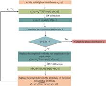
Compared with using the light interference of two actual beams to obtain holograms, computed holography has the advantages of low noise, simple operation, high repeatability, and holographic reproduction of virtual objects. Meanwhile, computer-generated holography technology is commonly used to reconstruct arbitrary images and is widely used in virtual reality, advertising and anti-counterfeiting systems. Terahertz wave refers to the electromagnetic wave between 0.1 THz~10 THz, between millimeter wave and far infrared wave. The unique spectral position of terahertz waves gives it the advantages of low photon energy, rich spectral information, strong penetration ability, and large bandwidth. Based on the above characteristics, terahertz holographic technology is widely used in biomedical imaging, safety screening, non-destructive testing, and evaluation fields. However, limited by the inherent refractive index of natural materials, traditional propagation and reflective terahertz functional devices are usually composed of High-density Polyethylene (HDPE), Polytetrafluoroethylene (PTFE), Polymethylpentene (TPX), quartz and sapphire, which inevitably leads to their large size, heavy weight and low efficiency, which hinders the development of miniaturization and integration of terahertz systems. Metasurface refers to a two-dimensional array of sub-wavelength artificial unit structures arranged on a plane. It can flexibly adjust the wavefront amplitude, phase, polarization, and orbital angular momentum through ease of integration and manufacturing, with the potential to control electromagnetic waves flexibly. It retains the advantages of electromagnetic regulation of three-dimensional metamaterials, and its preparation difficulty and propagation loss are significantly reduced due to its planar structure characteristics. The design of a suitable metasurface element structure can afford the capability to modulate the optical field flexibly, thereby enabling the realization of diverse functionalities, such as beam focusing, beam diffraction, generation of specialized beams, beam shaping, and holographic image reconstruction.Based on the above research background, this paper uses the GS algorithm to obtain the optimal solution distribution of the target object's phase. Then it uses the all-silicon rectangular column as the basic unit structure to arrange metasurface-regulated terahertz waves to achieve holographic imaging. This research proposes a new type of meta-atom structure, the all-silicon rectangular column, as the fundamental building block for the terahertz metasurface. This design overcomes the drawbacks of traditional metal-based metasurfaces, such as high ohmic losses and low polarization conversion efficiency, by implementing Mie-type electrical resonance and magnetic resonance or an effective waveguide effect. These phenomena result in the modulation of wavefronts at terahertz frequencies. Different phase regulation methods are used to design metasurfaces to achieve holographic imaging with different functions. Metasurfaces based on geometric phase control can realize holographic imaging and verify that the obtained image has a specific broadband.On this basis, the rational design of the metasurface element structure realizes a circular-bias multiplexing function based on the simultaneous regulation of the geometric phase and propagation phase. The specific function realized is to obtain holographic images of the letter E when right-handed circularly polarized light is incident light. When left-handed circular polarized light is incident, a hologram of the letter F is obtained. Compared with the holographic diffraction efficiency obtained by using metasurfaces made of metal, the diffraction efficiency of holograms can be effectively improved by using the all-silicon column structure. To a certain extent, this design solves the shortcomings of considerable size, heavy weight and low efficiency of traditional functional devices in the terahertz band and promotes the development of integrated and multifunctional terahertz technology in the terahertz band. It shows excellent potential for holographic imaging and wavefront regulation applications. The polarization multiplexed holographic imaging proposed in this paper can store multiple pieces of information in one carrier, set the incident light in different polarization states to obtain different information, and present different holograms. The implementation of this approach utilizing the metasurface can result in the enhancement of multi-channel holographic imaging, thereby significantly increasing the utilization efficiency of the metasurface technology. This not only has significant potential in terms of large-scale information storage but also has potential applications in polarized optics and holographic data encryption.
Aug. 25, 2023Vol. 52 Issue 8 0809001 (2023)
Rui GONG, Yalin GENG, Li PEI, and Huai WEI
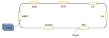
Self-similarity is a relatively common natural phenomenon, which is also found in pulses transmitted in optical fibers. Self-similar pulses are parabolic pulses. In fiber amplifier, pulses can evolve into such parabolic pulses under the combined influence of gain, normal dispersion and nonlinearity. This is the definition of self-similar pulses in early research. When a pulses is transmitted under this condition, not only does the shape gradually evolve into a parabolic shape, but the shape of the pulse can be maintained, and the pulse width and power are amplified at the same time. The evolved self-similar pulse has a linear chirp curve, which can achieve long distance relative transmission without pulse splitting in the case of high power. Therefore, self-similar pulses are also applied to the mode-locked fiber laser. Although the fiber laser cavity is different from the fiber amplifier, the self-similar pulse in the cavity still has the characteristic of anti-splitting, which improves the output pulse energy of the mode-locked fiber laser. The gain fiber of the self-similar fiber laser also basically meets the generation requirements of the initial self-similar pulse, but these requirements are difficult to achieve for current mid-infrared fiber lasers. In the mid-infrared band, the fiber is usually in the anomalous dispersion region. If the wave guide dispersion and doped rare earth of the gain fibre are adjusted substantially, it will bring extreme difficulties to fiber fabrication. Self-similar pulse fiber lasers are mainly divided into passive self-similar fiber lasers and active self-similar fiber lasers. Active self-similar fiber lasers usually require spectral filtering, where the pulses in the cavity evolve into self-similar pulses in the gain fiber part. Therefore, the gain fiber of the active self-similar lasers must be normal dispersion, which is difficult to adapt to the gain fiber with anomalous dispersion in the mid-infrared band. In the passive self-similar fiber laser, the self-similar evolution is in the passive fiber with normal dispersion. Even if there is a passive fiber with anomalous dispersion in the laser cavity, the self-similar pulses can still be output as long as the net dispersion of the laser system is positive. Dispersion-managed fiber laser, usually specifically a dispersion-managed soliton fiber laser, is a laser with dispersion map structure, and also generally refers to all fiber lasers that control dispersion in the cavity. Whether the dispersion-managed cavity with anomalous dispersion gain fiber can become a passive self-similar fiber laser and output self-similar pulses with comparable quality should be further researched. For the sake of comparison, this paper, first systematically summarizes the historical evolution, classification system and respective characteristics of mode-locked fiber lasers with normal dispersion. Then, the dispersion-managed mode-locked fiber laser with anomalous dispersion gain fiber is studied by numerical simulation. Through the analysis of time domain shape, spectrum, pulse energy, pulse width and chirp curve linearity and comparison with several traditional self-similar pulse fiber lasers constructed by normal dispersion gain fibers with mirror dispersion characteristics, it is pointed out that the laser system completely conforms to the features of passive self-similar fiber laser, and can achieve the effect of traditional passive self-similar fiber laser constructed by normal dispersion gain fiber. The realizable range of self-similar pulse fiber lasers is expanded theoretically, which makes up for the theory deficiency of traditional self-similar pulse fiber lasers in this aspect. In addition, the influence of dispersion map, net dispersion in the cavity and dispersion compensation nonlinearity on the output pulse of the laser system is discussed in detail, which provides a new idea for generating higher quality ultrashort pulses in the mid-infrared band using anomalous dispersion gain fiber.
Aug. 25, 2023Vol. 52 Issue 8 0814001 (2023)
Zhichang XIA, Yongai YU, and Jianhua SHANG
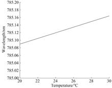
With the continuous development of laser technology, semiconductor lasers have made rapid progress in many aspects, such as electro-optical conversion efficiency and output optical power. Because of their small size, high efficiency, low cost, and easy integration with related devices, they are widely used in laser radar, optical sensor detection, beauty, industrial processing and other fields. The central wavelength and output power of semiconductor lasers are easily affected by the driving current and operating temperature. Because the excitation mode of semiconductor laser is direct electrical injection, the stability of injection current directly affects the central wavelength and output power of semiconductor laser. In the process of electro-optical conversion, due to non-radiative composite loss, free carrier absorption and other loss mechanisms, a part of the injected current is inevitably converted into heat. When the working temperature of the laser increases, the reduction of the external differential quantum efficiency and the increase of the threshold current can lead to the reduction of the output power of the semiconductor laser. Temperature rise can also lead to changes in the refractive index and band gap of the semiconductor laser material, thus changing the size of the resonator, and finally the central wavelength of the semiconductor laser will shift red. In addition, the service life of semiconductor laser will be greatly reduced if it works in a high temperature environment for a long time. Excessive temperature rise may reduce the service life by an order of magnitude. In order to solve the problem of driving current and working temperature stability, and to obtain accurate, stable and reliable detection results, a STM32 based medium and low power semiconductor laser driving power supply and temperature control system is designed. The traditional laser power control method is the constant power control based on the photoelectric feedback principle. Due to the serious temperature drift of the photoelectric detector, the power control effect is poor. Traditional laser temperature control uses an integrated semiconductor cooling chip to drive the chip. The circuit is complex and the adjustment time is long. The power control of this design adopts constant voltage control mode. The driving power supply uses a deep negative feedback circuit, and forms a double closed-loop power control with software PID, avoiding the use of photoelectric detectors, which has better power stability in comparison. An H-bridge driving chip and PID algorithm are used to control the temperature of the semiconductor laser. The experimental results show that the driving current stability of this design is excellent, with a stability of about 0.3%, and an accuracy of 0.86%; the temperature adjustment speed is fast, the control accuracy of long-term working temperature is ±0.03 ℃, and the stability can reach 0.18%; the output power of the laser is stable within ±2 mW; the fluctuation range of the central wavelength of the laser is 0.007 5 nm. The power and wavelength under the constant power control mode are also tested. The experimental results show that the power and wavelength under the constant voltage control mode are more stable than that under the constant power control mode. The drive system integrates power control and temperature control, which can meet the working requirements of the laser and can be applied to the same type of semiconductor lasers.
Aug. 25, 2023Vol. 52 Issue 8 0814002 (2023)
Xiang ZOU, Songfeng YIN, Yue CHENG, and Yunlong LIU
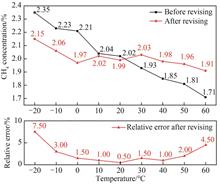
Laser methane sensor has obvious advantages of anti-poisoning, anti-interference, and long service life. It can be used for real-time online monitoring of natural gas leakage in complex environments. However, the laser methane sensor is easily affected by temperature, resulting in a large difference between the actual measured CH4 concentration and the actual value. Common temperature compensation algorithms include polynomial fitting method and empirical formula method. These two temperature compensation methods have a good effect on temperature compensation under the influence of single factor. However, the influence factors of temperature on the laser methane sensor include gas molecules, optical elements and circuit elements. Therefore, in the actual quality application, there is still a large error between the corrected concentration value and the true value.In this paper, a temperature compensation model is established by using the deep learning method. Its prediction accuracy mainly depends on the network model structure and large-scale training samples. In order to effectively improve the detection accuracy of the laser methane sensor in a wide temperature application environment, combined with industrialization, a large-scale laser methane sensor high and low temperature detection sample data set was established, and the model effect was further improved through big data training.Based on the model framework, an ISSA-BP algorithm with global optimization capability is proposed. Firstly, a quasi-reflective learning strategy is used to initialize the sparrow population to improve the efficiency of iterative optimization. Secondly, we use the strategy of searching for prey in CSA to improve the location update of explorers in SSA, so that the algorithm has the ability to jump out of local optimization. At the same time, Levy flight strategy is introduced to improve the anti-predator position update and enhance its global search ability. Finally, the artificial rabbit disturbance strategy is used to update the sparrow individuals to further reduce the probability of the algorithm falling into the local optimum. By using the standard sparrow search algorithm, particle swarm optimization algorithm and grey wolf optimization algorithm to test unimodal function and multimodal function, the advantages of ISSA in terms of convergence accuracy and speed, global search and local development capability are verified.In terms of data, the training effect of the temperature compensation model is improved and the prediction error of the model is reduced by establishing a large-scale experimental data set of sensors with different temperatures and concentrations. In the temperature range of -20 ℃~65 ℃, 15 800 groups of sensor measurement data were used to carry out comparative experiments on BP, PSO-BP, SSA-BP and ISSA-BP temperature compensation models. The results show that the maximum relative error of the predicted value of temperature compensation model based on ISSA-BP neural network is only 0.52%, which is 7.70%, 2.46%, and 0.74% less than that of BP, PSO-BP, SSA-BP models respectively. When the temperature changes from -20 ℃~65 ℃, the predicted value of concentration still fluctuates in a small range. The Average Absolute Percentage Error (MAPE) of BP neural network, PSO-BP neural network, SSA-BP neural network and ISSA-BP neural network for predicting the test sample of 0.5% standard concentration methane gas is 0.038 6%, 0.014 6%, 0.005 8%, and 0.002 7%, respectively. Compared with other models, the values of MAE, MAPE, RMSE and RE of ISSA-BP neural network model are smaller, which indicates that ISSA-BP temperature compensation model has higher accuracy and better stability.The research results show that the algorithm in this paper can greatly improve the detection accuracy of the laser methane sensor in a wide temperature application environment, and is of great significance in improving the environmental applicability of the laser methane sensor.
Aug. 25, 2023Vol. 52 Issue 8 0814003 (2023)
Wenxuan CHEN, Min HE, Ping CHEN, and Qi CHEN
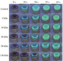
Solution-processed Perovskite Light-Emitting Diodes (PeLEDs) has drawn much attention due to their low cost, narrow emission spectra and wide color gamut. However, undesirable pinholes and defects of perovskite films impair device performance, which is attributed to the atactic nucleation and rapid crystallization during solution processing. In general, the antisolvent is added to the perovskite spin coating process to quickly remove excess solvent and form an intermediate phase. Combining with annealing treatment, mesophase gradually transforms into the perovskite phase and dense perovskite film can be obtained. At the same time, the larger organic cation (PEA+, TEA+, etc.) will cut continuous lead halide octahedron into the periodic quantum well structure to form quasi-two-dimensional perovskite which has a larger exciton binding energy and rapid energy transfer.By adding the large polymers to the precursor, long segments cannot enter the perovskite lattice and act as the “framework” in the perovskite crystallization process, which can restrict nucleation sites, inhibit the rapid growth of grains and further optimize the film quality. However, the size, fluidity and solubility of the polymer change with the increase of the segment length, which significantly affects the growth of perovskite crystals. Therefore, it is crucial to systematically study the regulation law of polymer segment length on the crystallization kinetics of perovskite to improve the quality of perovskite thin films and thus promote the electroluminescence properties.Polyvinyl Pyrrolidone (PVP), a common non-ionic polymer, its structure is relatively simple and carbon segment length can be accurately controlled by molecular weight. Moreover, PVP contains a carbonyl group, which can effectively passivate the defects in perovskite. In this work, perovskite crystallization kinetics has been tuned by the incorporation of Polyvinyl Pyrrolidone (PVP) with different segment length. Based on in-situ photoluminescence and X-Ray Diffraction (XRD) spectra, it showed that perovskite crystallization rate is retarded to inhibit small n phase formation by increasing the PVP segment length, which played an important role in determining perovskite film quality, such as crystallinity, charge carrier recombination and roughness, etc. After different segment PVP was added to the precursors, the absorption peaks at 403 nm(n=1), 434 nm(n=2) and 465 nm(n=3) in the Ultraviolet-Visible Spectrum of the quasi-two-dimensional perovskite low-dimensional phase are significantly inhibited, which are considered adverse to Photoluminescence performance. According to space charge limited current tests, compared with films without additives, the defect density of the films decreased significantly after adding different segment PVP, reaching the minimum at PVP-10 kDa. And with the segment length continuing to increase (>10 kDa), the defect density will increase slightly. The short PVP segment (≤3 kDa) was not effective on adjusting the crystallization rate, resulting in minor improvement in roughness and photoluminescence quantum yield (PLQY) of the perovskite film. While the too-long PVP segment (≥30 kDa) inhibited crystallization, leading to high roughness, low crystallinity and deteriorated PLQY of the perovskite film. 1With the suitable PVP segment length (~10 kDa), the perovskite crystallization kinetics can be optimized, which exhibited decreased roughness from 1.489 nm to 0.954 nm, decreased defect density from 1.55×1018 cm-3 to 1.05×1018 cm-3, improved PLQY from 16.9% to 58.9%. Combined with superior morphology and PLQY of the perovskite films with PVP-10 kDa, it is promising to achieve a high electroluminescence performance. The PeLEDs before and after incorporation of PVP-10 kDa were prepared with a stacking structure ITO/ PVK/Perovskite/TPBi/LiF/Al. Compared with the control devices, the PVP-10 kDa devices showed little change in luminance but significantly reduced current density, which benefited improved maximum external quantum efficiency (EQE) from 8.55% to 18.00%. This work systematically investigated polymer segment length dependent perovskite crystallization and electroluminescence performance, which provides a guideline to design polymer additives to further promote the development of PeLEDs.
Aug. 25, 2023Vol. 52 Issue 8 0816001 (2023)
Gonghe DU, Xudong HU, Qianwen YANG, Yonggang XU, Zhaoyu REN, and Qiyi ZHAO
Once graphene was discovered, it has attracted the attention of the scientific community because of its excellent mechanical, electrical and optical properties, and has pushed the development of nanotechnology to an unprecedented height. Two-dimensional (2D) Transition Metal Chalcogenides (TMDs), as an important part of nanomaterials, not only inherit the excellent physical properties of Graphene, but also make up for the shortcomings of photoelectric applications caused by the zero-band gap and semimetal properties of Graphene. It is found that transition metal chalcogenides have widespread application value in photoelectric devices, spintronics, catalysis, biochemical detection, supercapacitors, solar cells, lithium ion batteries and other fields. It is worth noting that two-dimensional Janus structural materials, as a new type of two-dimensional layered nanomaterials, have more abundant photophysical properties than traditional transition metal chalcogenides on account of the different types of atoms on both sides of the transition metal in the Janus structure, and their various surface interface structures that provide convenient conditions for the construction of different types of heterojunctions. Therefore, the calculation and analysis of the photoelectric properties of two-dimensional Janus structural materials and related heterojunctions has been an important aspect of theoretical research on two-dimensional layered nanomaterials in recent years. At present, there are relatively few reports about the dielectric properties of two-dimensional Janus materials, and the analysis of the generation mechanism of dielectric properties needs to be further strengthened.The traditional density functional theory has become an indispensable calculation method for the theoretical study of the physical properties of multiparticle systems. Due to the existence of van der Waals interaction in 2D layered nanomaterials and the tremendous influence of electron orbital hybridization on their photoelectric properties, we use density functional theory, van der Waals correction and hybrid functional to calculate and analyze the multi-particle system to obtain a result close to the experiment.First, the electronic properties and optical dielectric functions of Janus structural materials MXY (M=Zr, Hf; X/Y = S, Se) and its related heterojunctions are calculated and analyzed. It can be found that the results of the band gap values of the IVB-VIA Janus structure material are in good agreement with the experimental values after correction by first principles with hybrid functionals HSE06. The electronic structures indicate that the monolayer ZrSSe and HfSSe are indirect bandgap semiconductors with band gaps of 1.196 0 eV and 1.040 2 eV, respectively. The remarkable band nesting that appears on band structure means light-matter interaction strongly. By comparing the state densities of the materials, it can be found that the positions of the Conduction Band Minimum (CBM) and the Valence Band Maximum (VBM) of the two structures are mainly related to the transition metal atoms and chalcogens atoms, respectively. The correlation analysis of dielectric properties and band structure shows that the appearance of the peak is mainly related to the electron transition occurring between the first, second and third valence bands and the first, second and third conduction band after the absorption of photons. In addition, due to the p orbital electron transition of S and Se atoms, the material exhibits excellent photon absorption properties in the infrared and visible regions. The local planar-averaged DOS proves the existence of three kinds of heterojunctions based on ZrSSe and HfSSe with different interface characteristics and the charge density associated with the band edge is distributed over both materials. Notably, the absorption peaks of ZrSSe/HfSSe heterojunctions are in the infrared and visible range, up to 1.26×106 cm-1. At the same time, the calculation of the energy loss spectrum also shows that ZrSSe/HfSSe heterojunctions has a high absorptivity in the range of visible light. This work not only effectively reveals the photophysical properties of Janus structural materials and their heterojunctions, but also promotes the potential applications of these materials in new types of optoelectronic devices.
Aug. 25, 2023Vol. 52 Issue 8 0816002 (2023)

Jiajun CHEN, Kaixiang LI, Renjian LI, Chunlei SHAO, Guiye LI, and Lingling CHEN
The optical endoscope imaging technology based on fiber bundle has the advantages of strong flexibility, no radiation and ease of integration. However, the structural characteristics of the fiber bundle inherently cause the honeycomb grid artefacts. In addition, the endoscope microlens introduces image distortion and low numerical aperture. As a result, there is a substantial decrease in the image quality for such endoscopic systems. In order to address this challenge, tremendous efforts have been made and a number of algorithms have been developed, such as spatial/frequency domain filtering, interpolation, etc., to successfully eliminate the image grid artefacts introduced by fiber bundle. Nevertheless, the image quality has not been substantially improved especially in terms of reduced spatial resolution and image distortion. In recent years, the image recognition and enhancement capabilities of Deep Learning (DL) have been significantly improved and thus, DL has been explored to apply for the reconstruction of endoscopic images, for example, using U2-Net, Attention U-net, and GARNN models. While the image quality could be improved to some extent, it remains challenging in the restoration of fine details. More importantly, until now, there has been no research on the utilization of DL to eliminate image distortion introduced by microlens in the endoscopic image. In order to address this challenge, we develop a new open source algorithm AtG-DeepLab V3+ by effectively integrating the self-attention mechanism and the DeepLab V3+ network for the enhancement processing of endoscopic images. This developed model adapts the coding-decoding network as a whole architecture and uses the ResNet101 network to extract features. Encoding context information by probing incoming features at multiple rates and multiple valid horizons or merging operations allows high-level abstract features to be extracted and clearer objects to be captured by progressively recovering spatial information. The self-attention gate integrated with the model decoder can effectively suppress the activation of irrelevant regions, better realize the screening and extraction of important spatial features of images, and achieve the distortion correction and high detail restoration of the endoscope image. In addition, we develop an optical endoscopy imaging system to collect test target images and biological tissue images for model training and testing. The training results of test target images demonstrate that the developed AtG-DeepLab V3+ model can effectively correct the intrapexial image distortion and remove the honeycomb grid structure artefacts. The results of local detail magnification and comparison illustrate that this model has a good performance in improving the image resolution limit and detail feature extraction compared with other current models (i.e., U2-Net, Attention U-net and GARNN). The training and testing results of biological tissue images exhibit that the fine detailed features of human tissue can be extracted by the AtG-DeepLab V3+ model, and the distortion of the pattern can be effectively eliminated. The recovered images show a clearer tissue texture and richer fine details, which are highly similar to the real images. Compared with the existing U2-Net, Attention U-net and GARNN algorithms, the AtG-DeepLab V3+ model can achieve a much higher peak signal-to-noise ratio (increased by 66.4%, 51.9%, 154.6%), structural similarity (increased by 55.6%, 45.9%, 231.5%), demonstrating a significant improved enhancement effect of endoscopic image. We believe that this algorithm can provide a new efficient processing scheme for optical endoscopy image processing.
Aug. 25, 2023Vol. 52 Issue 8 0817001 (2023)
Muqing ZHANG, Yutong HAN, Bonian CHEN, and Jianxin ZHANG
Brain tumors are abnormal cells that grow in the brain or skull, and malignant brain tumors always cause great danger to the life and health of patients. Magnetic Resonance Imaging (MRI) can produce high-quality brain images without damage and skull artifacts, and it is currently one of the main technologies for the diagnosis and treatment of brain tumors. Meanwhile, the automatic segmentation of MRI brain tumor lesion regions is of great significance for the clinical diagnosis, surgical planning, and postoperative evaluation of brain tumor patients. However, due to the complexity and diversity of brain tumor images and the difficulty in obtaining the large-scale high-quality brain tumor segmentation dataset, it is still a difficult task to achieve high-precision automatic segmentation of MRI brain tumors. In recent years, with the breakthrough development of deep learning in computer vision tasks, it has also been successfully applied in the field of medical image analysis, and has achieved significant performance improvement in a number of medical image analysis tasks. Among them, U-Net, with its simple architecture and high performance, has become a mainstream model to solve a series of medical image segmentation tasks, including brain tumor segmentation. To this end, according to the advantages of the U-Net network architecture, focusing on issues of large variation of tumor spatial information and small number of finely labeled samples, a novel brain tumor image segmentation method, called Multi-scale Ghost Generation Adversarial Network (MG2AN), is proposed by combining U-Net with unsupervised generative adversarial network. MG2AN leverages the 3D U-Net model as a generator to obtain brain tumor segmentation results, and introduces 3D PatchGAN corresponding to multi-scale feature information of the generator as a discriminator to judge brain tumor segmentation results and ground truth, and the whole model is trained by adversarial learning. To improve the MRI brain tumor segmentation effect, a ghost module is introduced in the encoding stage of the generator, so that the ghost image and convolution feature map can be captured simultaneously during the convolution process, thus improving the brain tumor generation results of the generator. Considering the computational cost and the degree of information loss, the ghost module is only introduced in the final stage of the encoder. Meanwhile, multi-scale feature fusion is proposed in the decoding process to obtain three different brain tumor segmentation results for detail information, local information and global information, and then three kind of feature information for different emphasis are fused to further boost the segmentation performance in adversarial learning. To train the model, the loss of generated adversarial segmentation network is first back-propagated during the training process, and the new loss value is calculated based on the brain tumor segmentation results with the ground truth. Then, the two parts of the loss value are combined into the final loss value to jointly supervise the network. In addition, considering the obvious differences in grayscale and contrast of brain tumor images from different modalities, the Z-score method is utilized to normalize the image data in preprocessing. Meanwhile, to reduce the influence of large amount of useless background information in brain tumor images, the multi-modal 3D MRI brain tumor images are randomly cropped to a size of 128×128×128 as the input of the network. The data augmentation strategies such as random flip and intensity transformation are also adopted to guarantee the segmentation accuracy and generalizability of the model. The proposed MG2AN model is extensively evaluated on the public BraTS2019 and BraTS2020 brain tumor image datasets via ablation experiments, comparison experiments, and visualization results. The dice values of whole-tumor, core-tumor, and enhanced-tumor segmentation obtained by MG2AN on the BraTS2019 validation set are 0.902, 0.836, and 0.77, respectively. Meanwhile, the corresponding dice values on the BraTS2020 training and validation data sets are 0.902/0.903, 0.836/0.826 and 0.77/0.782, respectively. Compared with the baseline network, the dice values of MG2AN on the BraTS2020 training and validation data sets increase by 4.1%/1.3%, 2.2%/0.9% and 5.7%/2.7% on the whole tumor, core tumor and enhanced tumor, respectively, demonstrating the effectiveness of introducing generative adversarial networks and the improved generators. When comparing MG2AN with the state-of-the-art methods in the field of brain tumor segmentation, it can show comparable or better performance by considering both dice and Hausdorff 95 evaluation results. Finally, it also can be carried out that the segmentation effectiveness of MG2AN model is better than the baseline model in the visual evaluation of brain tumor segmentation. Therefore, the comprehensive experimental evaluation and analysis results demonstrate the effectiveness of the proposed MG2AN for the brain tumor segmentation task.
Aug. 25, 2023Vol. 52 Issue 8 0817002 (2023)
Xiongwei WU, Jianan ZHANG, Long CHEN, Zhuochen LOU, Qian MA, Shuo LIU, and Jianwei YOU
Topological photonics is an important and rapidly growing field that offers a powerful way to manipulate light. The geometric and topological ideas in this field have thoroughly changed our understanding of light propagation. Floquet topological insulators are an important branch of topological photonics, where many novel physical phenomena are waiting to be explored. This is mainly due to the condensed matter community, which utilizes periodically driven systems to reveal new phases of matter that do not exist in equilibrium systems. This paper reviews the research on Floquet topological optical insulators over the last decade, starting from a classification of their implementations as time-based modulation, space-based modulation and resonator-coupling-based modulation of Floquet topological photonic insulators. More specifically, time-modulated Floquet topological photonic insulators represent a unique class of artificial photonic structures with special topological properties, characterized by the dynamic modulation of topological phase through a periodic time function. This modulation method introduces a distinct control mechanism to photonic systems, leading to an unprecedented light transport. A key feature of time-modulated Floquet topological photonic insulators is the realization of topological edge states by breaking time-reversal symmetry. These edge states can propagate unidirectionally along the system boundaries and exhibit robustness against defects and back-scattering. Compared with traditional static topological photonic insulators, the time-based modulation method introduces a new degree of freedom in the temporal domain, thereby offering a wider range of control strategies and application potential. Given the theoretical limitations of time-modulated Floquet topological photonic insulators along with experimental constraints due to the inability of active switching frequencies to meet experimental demands, practically experimental demonstrations in this field have encountered significant restrictions. To address this challenge, researchers have initiated the exploration of alternative methodologies. Among these, space-based Floquet topological photonic insulators have emerged as a noteworthy direction. This approach employs one spatial dimension as a surrogate for the time dimension, thereby enabling the realization of pertinent topological properties in Floquet topological photonic insulators without requiring additionally high switching frequencies. Therefore, this approach has garnered significant attention and achieved substantial progress in the field. However, due to the incompatibility with integrated photonic systems, the integration of temporal or spatial modulation on a semiconductor platform remains a challenge. To address this issue, the two-dimensional structure of coupled resonator optical waveguides has emerged as a robust platform for the study of topological photonic insulators, thanks to its unique structure and compatibility with traditional photonic integrated circuits. So far, research on Floquet topological photonic insulators based on coupled resonances is garnering increasing attention. In summary, we have demonstrated the unique topological properties and amazing physical phenomena as well as the broad research progress in applications are presented from both theoretical and applied aspects. The achievements and challenges in this field are reviewed and discussed, and further research on Floquet topological photonic insulators is foreseen.
Aug. 25, 2023Vol. 52 Issue 8 0826001 (2023)
Yuhong ZHOU, You ZHENG, Li XU, Ping YU, Zhen GAO, and Zhuoyuan WANG
The propagation of light is generally reciprocal. Optical reciprocity, also known as temporal inversion symmetry, is essentially the existence of reciprocal solutions supported by Maxwell's equations. However, traditional reciprocal optical components suffer from problems such as the optical diffraction limit, which limits their further development toward high performance. In recent years, with the rapid development of topological photonics, it has been found that topological photon states have one-way transmission properties with forward conduction and reverse blocking state. At the same time, local structural defects will not influence global properties in optical topology, therefore, non-reciprocal topological photon states have many excellent physical properties, such as immunity to obstacles and defects, which can ensure that the one-way transmission has strong robustness and consequently promises potential applications such as optical integrated circuits and nonlinear optics. Magneto-optical photonic crystals based on gyromagnetic materials are the earliest topological optical structures to realize non-reciprocal topological photon states. They are also the most commonly used topological optical structures to study the generation, interaction and novel topological optical phenomena of topological photon states, which still contain a series of physical mechanisms worthy of further exploration. However, an external magnetic field is required, which affects the integration of optical devices, the frequency is limited to the microwave, and the gyromagnetic material has a weak response to the magnetic field, so it is still difficult to realize the integer quantum Hall effect of light, thus limiting its practical application prospects.Magnetoplasma is a simple material with non-reciprocal, rotational and homogeneous medium. The maximum non-reciprocity can be achieved by optimizing the permittivity tensor or the permeability tensor since the strength of the non-reciprocity depends on the relative strength of the diagonal tensor elements and the off-diagonal tensor elements. According to the Onsanger-Casimir principle, the dielectric constant tensor of a magnetic plasma is asymmetric, which implies the breakdown of the Lorentz reciprocity. The near-field electromagnetic wave propagating at the interface of magneto-optical materials under the action of a magnetic field is called a magnetic surface plasmon, which has non-reciprocal transmission characteristics. The unidirectional waveguide structure based on magnetic surface plasmon not only has a local enhancement effect, but also can break the diffraction limit, which lays a solid foundation for the development of new optical functional devices with high performance, high resolution, and high integration in space environment detection. At the same time, we also note that non-reciprocal transmission based on plasmon may be subject to absorption interference, and its practical value needs further verification. The optical nonlinear effect is also one of the ways to achieve non-reciprocal transmission. To achieve non-reciprocal transmission, the most likely development direction is to design topologically protected nonlinear optical phenomena in accordance with the topological edge soliton phase formed by Hall edge states in photonic crystals. It is easy to realize the system integration without the external magnetic field to achieve non-reciprocal transmission. However, in order to achieve nonlinear effects, it usually requires extremely high electric/magnetic field strength or extensive use of nonlinear materials, which greatly limits its application. Finally, this paper also briefly discusses non-reciprocal transmission based on other principles, such as breaking optical reciprocity using time modulation, non-reciprocal optical transmission based on synthetic angular momentum, and the use of coupling characteristics between nonlinear resonators, and so on. Non-reciprocal optical transmission based on time, phase, and energy modulation, as well as losses, also faces instability issues. This is currently a major research direction in the field, with one potential solution being to design systems related to and protected by topology to realize non-reciprocal transmission, thereby reducing losses caused by reverse transport in optical devices. Additionally, we analyzed and looked forward to its future development trends and key issues it may face.
Aug. 25, 2023Vol. 52 Issue 8 0826002 (2023)
Zhizhuang LIANG, Qun HAN, Yuliang TANG, Teng ZHANG, and Zhenzhou CHENG
With the rapid increase of electrical power demand, the voltage level of power grid also improved. The traditional current transformer is difficult to meet the needs of power grid because of its easy saturation, poor insulation, narrow frequency band, etc. The optical fiber current sensor can solve these problems. Therefore, it has wide application prospects in power monitoring and smart grid construction. However, the nonlinear response of magneto-optical crystal is the main factor that limits the application of the magneto-optic fiber current sensor. Nowadays, research on the nonlinear error of the Fiber Optical Current Sensors (FOCS) mainly focuses on the nonlinear dependence of the Verdet coefficient of the Magneto-optical (MO) materials on the external temperature. The change of Verdet coefficient will lead to the crosstalk of magnetic field and temperature, which is one of the main factors limiting the practical application of the FOCS. Nevertheless, when the temperature is fixed, the output signals of the MO materials is also not changed linearly with change of the external magnetic field. To improve the accuracy of the sensors, we studied the source of the nonlinear response of the MO crystal theoretically and experimentally. In this paper, we demarcated the output curve of garnet crystal from no magnetic field to saturated magnetic field. Through simulation and experiment, we proved that the nonlinear response of MO fiber optical current sensor is caused by the diffraction characteristics of magnetic domain of the MO material. The model of magnetic domain effect proposed by us conforms to the output response of the MO sensors. Through the dual-channel demodulation method, we can calculate the intensity of the output light through the 45° polarization beam splitter according to Malus law. And we obtain the Faraday rotation angle according to the demodulation algorithm of difference division sum. The theoretical results show that the influence of nonlinear error caused by magnetic domain effect can be ignored with the method of the two-channel demodulation. And in this way, the influencet of light source fluctuation can be eliminated. Simulation and experimental results show that the nonlinear error at a fixed temperature is mainly due to the voltage conversion coefficient mismatch of the two photodetectors and the assembly error of angle between polarizer and polarization beam splitter. Although the nonlinearity seems slight in macro performance, it is the key to affect the performance of the sensors in the case of high accuracy requirements. When the temperature changes, the nonlinear error of the MO materials is mainly due to the temperature dependence of Verdet coefficient on temperature. In order to solve the above problems and improve the accuracy of the MO fiber optical current sensor, we propose a nonlinear compensation model based on quadratic fitting. By comparing the four error models between the compensation model and the traditional demodulation model, the experimental results show that this method has good fitting accuracy and is suitable for nonlinear compensation of FOCS based on the MO material. In the actual experiment, we adjust the two magnifications to make the two conversion signals equal without applying the magnetic field. It means that the initial assembly angle error is compensated by adjusting the magnification. In this case, the result of the sensor output is the best. After that, the nonlinear law of the sensor is calibrated by the experimental data, and the external magnetic field is obtained by solving the quadratic function, which can significantly improve the accuracy of the sensor. This method has a simple structure and high fitting precision, and can meet the real-time acquisition of the MO fiber optical current sensor.
Aug. 25, 2023Vol. 52 Issue 8 0806001 (2023)
Ruimu YANG, and Xiaopeng DONG
Fiber optic Extrinsic Fabry-Perot Interferometers (EFPI) are frequently utilized in many acoustic sensing scenarios due to their simple structure, ease of fabrication, high sensitivity, high phase consistency, and strong resistance to electromagnetic interference. However, the cavity length of the EFPI sensor is susceptible to environmental variables such as temperature and air pressure, and the drifting of the orthogonal working point caused by the change of cavity length will lead to signal fading and distortion. Nevertheless, several demodulation methods are less practical or even ineffective when dealing with small signals: Dual-wavelength method for Mach-Zehnder interferometer is inconvenient to apply to the EFPI demodulation; the Ellipse-Fitting Algorithm's (EFA) Lissajous figure will degenerate into a straight line for small signals, and there are also the disadvantages of poor real-time performance and slow demodulation speed; the second-order Differentiate-and-Cross-Multiply (DCM) operation has wide applicability, but the Direct Current (DC) term must be accurately removed, for small signals, the removal of DC term is difficult; the Bessel method has the same difficulties as DCM, and it can only demodulate single-frequency signals; The method of using tunable laser feedback to control the orthogonal working point has the drawback of high cost, and lasers with wavelength scanning function have high requirements for hardware reliability; Phase Generated Carrier (PGC) technology requires a complex carrier modulation system with a limited frequency response range, and the system is complex and large when PGC uses piezoelectric transducer to generate phase carriers. In contrast, intensity demodulation has the advantages of a linear transfer function, simple signal processing, high sensitivity and is suitable for the detection of high-speed and small signal. JIANG Yi et al. proposed a Symmetrical Demodulation Method (SDM) suitable for unstable cavity length and unknown cavity length, which constructs two equal interference phase differences between the three output signals by selecting specific three wavelengths, and then recovers the phase of the signal through mathematical operations. This method has the advantages of large dynamic range and simple operation, and it is more suitable for the detection of large signals. However, in the case of small signals, the SDM algorithm may lead to increased noise and error in the demodulation result.If the wavelength of the light source is 1 550 nm, the interference phase of EFPI changes 0~2π, corresponding to the cavity length variation range of 775 nm. When the cavity length change caused by vibration is less than 30.11 nm, that is, the radian value in the interference phase is less than 0.22 rad, the approximate error of sinx and x is less than 1%. Under this condition, we can directly remove the DC term of interference signal reflected by EFPI to avoid the difficulty of distinguishing DC terms in small signals, Bsinφ4πns(t)λ can be regarded as the approximation of an interference signal. Three specific wavelengths are selected to construct two equal interference phase differences between the three output signals, and on the basis of these three signals, the two intermediate formulas can be compensated for each other to avoid the cancellation phenomenon, it ensure that at least one of the intermediate formulas has a better waveform, so as to obtain an intensity demodulation result with better Signal-To-Noise Ratio (SNR) and this approach is summarized as a Modified Symmetrical Demodulation Method (MSDM).Both theoretical analysis and numerical simulation demonstrate that MSDM performs better than SDM for small signals. Theoretical analysis indicates MSDM has a smaller and smoother error bound and relative condition number than SDM. In the numerical simulation, MSDM has less error than SDM in cavity length, frequency, and signal amplitude. After adding Gaussian white noise to the simulated signal, more high-frequency noise appears in SDM, while MSDM achieves superior demodulation results for the signal waveform. In the experiment, the SNR of the three signals ranges from 60~65 dB, and the experiment results align well with the simulation. Due to the complicated noise in practical applications and the high sensitivity of SDM, high-frequency noise appears in the demodulation results of SDM, resulting in a decrease in SNR. MSDM effectively improves the SNR of the demodulation results, the power spectra of MSDM's results are smoother than those of SDM, and the SNR near the main frequency increases from 74 dB to 86 dB. Values of cosδ measured in experiments consistently maintain between 0.55~0.7, in agreement with the theoretical predictions, thus confirming the reliability of MSDM. Additionally, the outputs of MSDM perform good linearity with the sound pressure of the speaker, and the linearity coefficient reaches 0.995 11. When the signal frequencies are 100 Hz, 500 Hz, 1 kHz, and 10 kHz, respectively, the MSDM demodulation results still have good SNR.An improved three-wavelength demodulation method for small signals of EFPI sensors is proposed by enhancing the existing three-wavelength phase demodulation algorithm. Our research group uses the approximate relationship of the sinusoidal function under small signal conditions to calculate the phase difference by calculating the intensity of the three signals, thereby solving the fading problem of EFPI interference signals. Through numerical analysis, simulations and experiments, it is proved that the proposed method has higher algorithm stability and smaller error in demodulation for small signals and better recovery on waveforms. Besides, the algorithm also theoretically has certain demodulation capabilities for non-periodic signals, which can potentially expand its application in the future.
Aug. 25, 2023Vol. 52 Issue 8 0806002 (2023)
Yao GUO, Xia ZHANG, Qiuping DU, Zhenshan YANG, and Xiaoguang ZHANG
While effectively enhancing the transmission capacity of current commercial single-mode optical fiber communication systems, Polarization Division Multiplexing (PDM) technology also faces serious challenges from Polarization Mode Dispersion (PMD) and Rotation of State of Polarization (RSOP). PMD causes the broadening of optical pulses, resulting in crosstalk and distortion of the signals, which may significantly increase the Bit Error Rate (BER) of the system. Also, RSOP might cause rapid change in the polarization state of optical signals up to several hundred krad/s, preventing the two polarization signals from being correctly separated at the receiver. In practical optical fiber links, PMD and RSOP usually coexist and impose significant impairments on the system performance. The main work of this paper is to build an impairment model of PMD and RSOP and to conduct a joint compensation of the polarization-relevant impairments.Traditionally, the Stokes formalism is employed to analyze the PMD and RSOP in commercial single-mode fibers that actually support two orthogonal polarization modes. The corresponding Stokes vector is a 3-dimensional real vector with clear physical meaning, and can be intuitively represented in the geometrical Poincare sphere. However, the Stokes formalism requires 3 auxiliary 2×2 Pauli matrices, and when extended to the treatment of Modal Dispersion (MD) and Mode Coupling (MC) in an N-mode optical fiber (i.e., a modal space of dimension N), a number of N2-1 auxiliary N×N Gell-Mann matrices are required, which can drastically complicate the analysis of MD and MC effects as N increases. Recently, borrowing methodology from quantum mechanics, we proposed and developed the Density Matrix (DM) formalism for the MD and MC in a modal space of arbitrary dimension N≥2. Without requiring any auxiliary matrices, the DM formalism is simple and straightforward in formulation and application, and is thus particularly suitable for the study of modal properties and signal compensations in the optical communication system.In this paper, we apply the DM formalism in the PDM system to construct a joint polarization-impairment compensation scheme. We establish a polarization impairment model for coexisting PMD and RSOP based on traceless Hermitian impairment matrices. By tracking the corresponding independent parameters in the matrices, we achieve the joint impairment compensation of PMD and RSOP. To verify the proposed scheme, we build a 28 GBaud PDM quadrature phase-shift keying coherent optical communication transmission simulation system, and implement a joint impairment-compensation for Differential Group Delay (DGD) over a wide range of 30~170 ps and fast RSOP over 300 krad/s~2 Mrad/s. In simulations, with about 100 iterations, the tracking and compensation have already converged for the impairment of 100 ps Differential Group Delay (DGD), and with only 0.5 dB and 0.7 dB optical Signal-to-noise Ratio (OSNR) cost, joint compensation of RSOP can be achieved in typical (600 krad/s) and extreme conditions (2 Mrad/s), respectively, both in the presence of 100 ps DGD. When 170 ps DGD and 2 Mrad/s fast RSOP coexist, the BER is 3.22×10⁻³, which still meets the criterion for error-free transmission of signals. The fast convergence, the small OSNR cost, and the stable BER performance verify the validity and efficacy of our polarization impairment model and the corresponding joint compensation scheme in optical communication systems.Furthermore, taking advantage of the DM formalism, our joint compensation scheme can be readily generalized to modal spaces of arbitrary dimension N for the impairment analysis and signal compensation of MD and MC, simply by the extending the relevant matrices from 2×2 to N×N. Therefore, our work potentially provide a simple and effective theoretical approach for the impairment analysis and compensation of optical-signals in more general mode-division multiplexing communication systems.
Aug. 25, 2023Vol. 52 Issue 8 0806003 (2023)
Xin GUO, Feng SHI, Tiantian JIA, Ruoyu ZHANG, Hongchang CHENG, and Yijun ZHANG
Negative Electron Affinity (NEA) GaAs photocathode, as the most promising Ⅲ-Ⅴ semiconductor photocathode for low-light image intensifier, has wide applications in underwater target detection, range gated imaging, and night vision. According to the photoemission theory of transmission‐mode GaAs photocathode, the incident light needs to pass through AlGaAs window layer before it can be absorbed and converted into photogenerated carriers by GaAs emission layer. The performance of image resolution on GaAs photocathode could result from the resolution of optoelectronic image and optical image. The resolution of optoelectronic image is determined by the longitudinal diffusion of photoelectrons in the emission layer. The resolution of optical image is mainly affected by the scattering of incident photons on the rough surface of the window layer. Most research on GaAs photocathode has focused on obtaining a higher optoelectronic image resolution, but there is rare research concentrated on improving the optical image resolution. However, the resolution of transmission-mode GaAs photocathode is hard to improve due to the ignorance of the optical image resolution. In order to study the image resolution of the transmission-mode GaAs photocathode under different wavelengths of incident light, a theoretical model based on the Scattering Transfer Function (STF) for the analysis of interfacial scattering from the AlGaAs window layer is proposed. A transmission-mode GaAs photocathode was fabricated, and the degradation of the incident optical image caused by the interfacial scattering of the AlGaAs window layer was quantitatively analyzed based on the signal-to-noise ratio fitting with reference peaks by using the variation of the STF and the Point Spread Function (PSF). The STF of the AlGaAs window layer rough surface under different incident light wavelengths was calculated and the incident light wavelength was set as 530 nm, 700 nm, and 830 nm respectively. The obvious characteristic is that the value of STF is improved when the incident light wavelength increases. Therefore, When the wavelength of incident light is reduced from 830 nm to 530 nm, the reduction of STF means that the area or integral value enclosed by the surface transfer function is smaller, resulting in the smaller the capacity of optical image information and the more blurred the imaging. The PSF of the AlGaAs window layer rough surface can be obtained by Fourier quasi-transform based on the STF. The results show that the central value of the PSF increases with the increase of the incident wavelength, which means the central energy of the optical image plane becomes more concentrated. In order to analyze the imaging quality of the third generation low light level image intensifier due to the scattering of incident light with different wavelengths on the rough surface of AlGaAs window layer, the PSF is convoluted with the original image of the given standard resolution target to simulate image degradation. When the incident light wavelength increases from 530 nm to 830 nm, the peak signal-to-noise ratioafter image degradation increases from 26.31 to 27.65, increasing by 5.1%. Computational results indicate that under the same surface roughness, compared with the incident light with the wavelength of 530 nm, the incident light with the wavelength of 830 nm is more beneficial to obtain a larger central value of the scattering transfer function and point spread function, which means that it is more conducive to obtain a sharper incident optical image. Furthermore, when the incident light wavelength is 850 nm, the signal-to-noise ratio of the image after scattering degradation is the highest, which also shows that the energy loss of the incident optical image is the smallest, the information capacity of the optical image is the highest, and the imaging quality is the best. This work will provide a reference for developing high-performance GaAs photocathodes.
Aug. 25, 2023Vol. 52 Issue 8 0812001 (2023)
Peiyuan XU, Bolun ZHENG, Zhen PAN, and Ciming ZHOU
Length measurement plays an important role in science and technology. From the three-dimensional coordinate measurement system of industrial manufacturing to the micro-scale and nano-scale microsystem, high-precision distance measurement plays a fundamental and crucial role. Due to the multiple characteristics of laser, such as high collimation and high coherence, laser ranging technology has been widely used in distance measurement. Some measurement methods based on frequency domain interferometry have been widely used in high-precision measurement. Compared with light wave, microwave can achieve more accurate frequency control and frequency measurement. A method called Optical Carrier-Based Microwave Interferometry (OCMI) has come out for high precision sensing. OCMI is similar to optical frequency domain interference. This method uses microwave modulated on broadband light, and then calculates the optical path difference with microwave phrase difference, therefore OCMI also has the advantage of high measurement accuracy. Because the frequency resolution of the microwave spectrometer is stronger than that of the spectrometer, the non-ambiguity distance of OCMI is greater than that of optical frequency domain interference. In addition, the broad-spectrum light acting as a carrier is not sensitive to transmission mode and dispersion OCMI can avoid the influence of inter-mode interference and polarization on ranging. OCMI has been widely used in fiber distributed sensing and fiber delay measurement. Taking the effective refractive index of the fiber as a constant, the length of the fiber can be calculated by the relationship between the length and the time delay.This paper proposes a ranging method based on optical carrier-based microwave interferometry. The microwave is modulated to broadband laser by electro-optic modulator. The Fiber Bragg Grating (FBG) reflects part of the carrier wavelength of microwave modulated light to realize the light splitting. The reflected light from FBG and the light reflected by the target are incoherently superimposed in the circulator. Due to the optical path difference between FBG and target, the microwave interference occurs after photoelectric conversion. The optical path difference is calculated by analyzing the frequency domain interference spectrum of microwave, and then the distance to be measured is obtained. In this paper, several sets of ranging experiments have been carried out to verify the feasibility of the method. This paper has carried out multiple sets of ranging experiments to verify the feasibility, the results show that a system stability of ±2.7 μm and accuracy of ±2.5 μm in 150~450 mm measurement range is achieved. The ranging system has high measurement stability and accuracy, which provides a new method for high-precision measurement.
Aug. 25, 2023Vol. 52 Issue 8 0812002 (2023)
Ying WU, Lihua DENG, Chaofeng MA, and Wei LIANG
Light Detection and Ranging (LiDAR) is a powerful ranging tool. Various types of LiDARs are widely used in atmospheric and oceanic sciences, such as laser altimeters, deep space exploration, and underwater target detection, most of which are based on time-of-flight. The integrated echo energy of pulsed LiDAR is inversely proportional to the square of detection distance. In order to achieve a longer detection distance, a pulse laser with high peak power is required. The longer the detection distance, the higher the peak power required. In order to achieve high peak power, complex and bulky lasers are usually needed. Meanwhile, the repetition rate of the laser is limited by the thermal damage threshold, which will reduce the point frequency of laser ranging. In order to achieve long detection distances with a low peak power lasers, some researchers have proposed a random code modulation continuous wave technology, which transmits a continuous laser with random pulse modulation instead of a single pulse. The distance information is obtained by cross-correlating the echo signal and the random modulation signal. Compared with a single pulse, the equivalent duty cycle of random code modulation is higher, so the peak power of the light source required to achieve the same integral energy is lower. It is possible to use miniaturized semiconductor lasers to achieve long-distance detection. In addition to using random intensity modulation for ranging, a random phase modulation laser ranging system based on heterodyne coherent detection has also been proposed. Heterodyne coherent detection can greatly improve the ranging sensitivity. More importantly, the target speed can be directly demodulated by measuring the Doppler frequency shift. However, the cross-correlation algorithm used for direct adjustment and detection of random intensity modulated laser ranging can not be directly transplanted to random phase modulated laser ranging system. A common solution is to sequentially shift the transmitted random sequence and multiply it with the echo heterodyne signal, and then perform FFT on the product results. When the shift amount is matched with the echo delay, the influence of random phase modulation will be canceled, and the Fourier spectrum will have obvious frequency peaks from which the Doppler frequency shift can be demodulated from the peak frequency of the spectrum. The computational complexity of this method is very high. The number of Fourier transforms required to complete a demodulation is equal to the length of the sampled data, which will occupy a large amount of computing resources and computing time. Some researchers have proposed a phase-encoded sub-carrier modulation technique. The spectrum of the detection signal has two components, low frequency and high frequency. The Doppler frequency shift can be extracted from the low frequency component, and the Doppler frequency shift compensation is performed on the high frequency carrier signal. The phase information of the echo signal is demodulated. The cross-correlation operation is performed on the phase information and the pseudo-random code. The target distance is calculated from the position of the cross-correlation peak. The drawback of this method is that the moving direction of the object cannot directly determined from the low-frequency signal. Some researchers propose to add a prefix without modulation before the phase modulation of the Pseudo-random Binary Sequence(PRBS). The echo signal during the prefix calculates the Doppler frequency shift. But this method will lead to a decrease in the measurement point frequency. In this work, a fast demodulation method is proposed for random phase modulated heterodyne detection laser ranging. It only needs five times of FFT to complete one demodulation, which is much less than the traditional demodulation method. Firstly, the Doppler frequency shift is obtained in the FFT spectrum of the heterodyne signal. The quadrature component of the echo signal is then digitally down-converted. The fast circular convolution of the transmitted random code of the echo signal is performed in the frequency domain. The distance information of the reflected target can be calculated from peak location of the the convolution results. In the experiment, the 11th-order PRBS with a length of 2 047 is used for phase modulation. The signal modulation rate is 40 MHz. The position and velocity information is correctly recovered from the echo signal using the proposed fast demodulation method. A distance resolution of 2.7 meters is achieved in the system.
Aug. 25, 2023Vol. 52 Issue 8 0812003 (2023)
Yue LI, Yinlin YUAN, Yingjie YE, Deyao KONG, Lan XIAO, Wenchao ZHAI, and Xiaobing ZHENG
High-precision radiometric performance test and calibration of field detectors are one of the important steps in the development of low-light level instruments and sensors. With the rapid development of low-light night vision instrument, photon microscope, low-light fluorescence imaging, biomedical imaging, and deep space exploration, higher requirements are put forward for the calibration light source of low-light level devices. Image intensifier is the core component of low-light night vision system, and its illuminance response range should be as low as 10-4 lx. The signal-to-noise ratio and optical gain of image intensifier play a decisive role in the imaging quality of the whole low-light detection system. To meet the high precision calibration requirements of low-light level sensors such as low-light image intensifier, a wide dynamic range low level illumination source with small volume and low power consumption is designed. Aiming at the requirements of the field radiometric response characteristics test of low-light level detectors, the design scheme, structure, and working principle of the wide dynamic range low-light level illumination source are first introduced. The wide dynamic range illumination source is composed of an adjustable dynamic range integrating sphere light source unit, a cylinder aperture and a feedback and control unit. The integrating sphere light source adopts the structure of child integrating sphere and parent integrating sphere. A halogen lamp source is built into the child integrating sphere, and the light is reflected several times inside the integrating sphere to achieve uniform brightness at the outlet. An adjustable aperture between the parent and child integrating spheres is used to realize the function of wide dynamic range flux adjustment. The area of the adjustable aperture determines the flux of light from the child integrating sphere into the parent integrating sphere. Compared with the way in which the flux of halogen light is regulated by the current of the source, it ensures that the color temperature of the light source is nearly consistent at different orders of magnitude of brightness output. The integrating sphere provides luminous flux to the monitoring detector and the cylinder aperture through two openings. The cylinder aperture is arranged at the outlet of the parent integrating sphere, and the position is coaxial with the parent integrating sphere outlet. The cylinder aperture is a cylindrical structure with an entrance aperture and an exit aperture, and has a stray light baffle inside, which can convert the brightness source of the integrating ball into a uniform illuminance source. Illuminance feedback and control module is used to display illuminance value of light source in real time and realize the setting of illuminance value. The dynamic range of low-light illuminance source is derived in detail, and the design parameters of light source are analyzed and simulated. Finally, the illuminance source performance test is carried out to verify the rationality of the design. The stability of the light source is tested. The standard detector is placed at the light source outlet to monitor the photocurrent of the detector. The test results show that the instability of the light source is less than 0.001 8%. The illumination feedback coefficient of monitor detector is calibrated by a standard illuminance meter, the illumination range of the light source measured by the monitoring detector is 3.8× 10⁻⁶ lx~12 lx. The experimental results show that the wide dynamic range low-light level illuminance source has many technical advantages, such as wide dynamic range regulation, high stability. In the field or laboratory environment, it has a certain application value for radiometric calibration and characteristic test of low-light level detector such as image intensifier.
Aug. 25, 2023Vol. 52 Issue 8 0812004 (2023)
Jinwei REN, Xiaowei CHEN, Bo WANG, Yan CAO, Yihan SUN, Xinyu LI, and Shenjiang WU
As society continues to progress, automobiles have become a common sight in households worldwide. However, the increase in the number of vehicles on the road has led to a series of traffic safety issues. As a result, automotive safety has become one of the most popular research topics worldwide. Among them, Head-Up Display (HUD) systems can be applied to cars, serving as an assistant to driving and improving driving safety. Through the use of a head-up display optical system, drivers can see virtual images that display important driving information and road conditions in the direction of their line of sight, eliminating the need to look down at instrument panel information and navigation information. This reduces driver distraction and improves driving safety. As HUD technology continues to advance and develop, it will gradually integrate with autonomous driving systems, becoming a standard feature in future high-tech vehicles. Nowadays, the technology of automotive HUD on the market is gradually maturing, mainly including Windshield HUD (W-HUD) and Augmented Reality HUD (AR-HUD). However, the current car-mounted HUD can only display virtual images on a single projection distance. When the driver changes the observation due to changes in vehicle speed, the visual focus distance needs to be adjusted to adapt to the HUD projection distance. Long-term and high-frequency adjustments can lead to eye fatigue for the driver. To address this issue, this paper proposes the design of a car-mounted binocular parallax optical system. Based on the current research status, a method of using a single DLP micro-projection machine to separate two images and generate two Projection Generating Units (PGUs) to display binocular virtual images for AR-HUD is proposed. According to the initial architecture of the HUD optical system, which is a coaxial reflection optical system, an off-axis reflection vehicle-mounted parallax display optical system is constructed by using an off-axis rotating reflection mirror. Then, by changing the object distance of the PGUs to the primary reflection mirror, the two free-form reflection mirrors are combined to construct an off-axis reflection binocular parallax vehicle-mounted display optical system, thereby ensuring the projection of two virtual images at different distances. The optical system uses a 5.74 inch DLP micro projector with an eyebox size of 130 mm×50 mm, a far projection field of view of 10°×3° and a near projection field of view of 4°×1°, and a virtual image projection distance of 3.8 m and 7.5 m. Image quality evaluation is analyzed and explained from the aspects of the point cloud diagram, MTF curve diagram, grid distortion, illumination curve diagram, and image simulation. The key to the optical system is tolerance analysis, which helps to determine the allowable limits of different manufacturing and alignment errors. Manufacturing and calibration errors can be reduced to an appropriate level without degrading the image quality of the optical system. If the tolerance requirements are too strict, it may increase the difficulty in processing and arranging the optical components and may also lead to unstable imaging quality during actual use. By designing the tolerance range of the curvature radius of the lens and the windshield usage area, the distance between lenses and the windshield usage area, the X-axis offset lens and the windshield usage area, the Y-axis offset lens and the windshield usage area, the axial rotation of the lens and the windshield usage area, and the axial rotation of the lens and the windshield usage area, the statistical results of the optical transfer function of the system's virtual image plane were obtained using Monte Carlo method with 1 000 randomly selected samples. It can be seen that at a spatial cutoff frequency of 4.42 1p/mm, more than 90% of the MTF of the optical system is greater than 0.63, indicating that the tolerance distribution of the system is reasonable, the tolerance capability is strong, and the design results are ideal. The design result of the dual-path AR-HUD optical system in this paper shows that, through software control, the near projection virtual image plane and the far projection virtual image plane can be displayed simultaneously or in a time-sharing manner, which improves the driver's visual experience.
Aug. 25, 2023Vol. 52 Issue 8 0822001 (2023)
Xiaowei YANG, Weifang YUAN, Tonghui LI, Yu LI, Xiaowen DONG, Kai LIU, Yongqing HUANG, and Xiaofeng DUAN
With the accelerated development of new industries such as big data and cloud computing, higher requirements are put forward for the capacity of communication networks. Due to the limitations of electrical interconnection, optical interconnection occupies an increasing proportion in the communication system. In order to meet the demand of rapid increase of optical communication network capacity, improving the transmission rate of single channel is an effective solution. Therefore, high speed optical detector is widely used in optical communication system. The goal of high speed optical detector is to obtain a higher bandwidth of 3 dB, and reducing the surface area of the device is an effective way to achieve it. The decrease of the mesa area can reduce the junction capacitance of the optical detector and thus improve the bandwidth of the optical detector. However, the decrease of the mesa area can reduce the optical coupling efficiency of the optical detector and directly increase the optical coupling loss in the system. To solve this problem, the monolithic integrated microlens structure on the back of high speed optical detector substrate is an effective solution. The structure increases the equivalent photosensitive surface of the optical detector, increases the optical coupling efficiency of the optical detector, and can effectively compensate the alignment deviation. An InP-based microlens structure integrated with a 1.31 μm optical detector chip is designed for data center applications. An InP-based microlens structure integrated with a 1.31 μm optical detector chip is designed for data center applications. An experimental method was developed to fabricate microlens glue by hot melt and transfer microlens glue by Inductively Coupled Plasma (ICP) etching. SiCl4 and Ar were selected as etching gases in ICP etching process to ensure the safety of the experiment. An InP-based microlens with diameter of 90.3 μm, crown height of 18.5 μm and smooth surface morphology was prepared. In this paper, a single InP microlens integrated on the back of the optical detector is designed, simulated and fabricated, which can improve the optical coupling efficiency of the device and compensate the alignment deviation. Through software simulation, the microlens with a diameter of 100 μm and a crown height of 18 μm can realize the convergence function at the focal length of 114 μm under two light incident angles of collimation and divergence of 10°, which meets the requirement of integration on the back of the optical detector. To prepare the microlens, the adhesive shape is first made, and then the adhesive shape is transferred to the substrate by etching to form the microlens. The adhesive shape of the microlens is made by photoresist hot melt method. Photoresist hot melt method is a common technology for microlens preparation. It can be used to produce microlens adhesive with the morphology and size meeting the requirements by using standard semiconductor equipment and technology. The method has high repeatability, good homogeneity and low cost. The microlens adhesive with smooth surface and no depression was prepared by photoresist hot melt method. The relatively safe SiCl4 and Ar were used for etching gas. By studying the influence of cavity pressure, etching gas flow and RF power on ICP etching, the ICP etching conditions of SiCl4 flow 13 sccm, Ar flow 13 sccm, pressure 0.266 Pa in the reaction cavity and RF power 105 W were finally selected. The InP microlens with diameter of 90.3 μm, arch height of 18.5 μm and smooth surface morphology was prepared. The responsivity of PIN light detector with backside monolithic integrated microlens was tested by source meter, optical fiber and probe station under incident light with wavelength of 1.31 μm. In the test process, the optical signal output by the laser with wavelength of 1.31 μm is incident into the optical detector through the fiber. The electrical signal generated by the optical detector enters the source table through the high-frequency line, changes the optical output power of the laser and records the corresponding optical current value on the source table, and finally calculates the responsiveness of the PIN optical detector. When the incident light of 1.31 μm wavelength is incident in the direction of 3° from the main optical axis, the response of the PIN light detector decreases by 4%. The prepared InP microlens meets the design requirements.
Aug. 25, 2023Vol. 52 Issue 8 0823001 (2023)
Yue ZHOU, Yaohui SUN, Haoyu WU, Mengjia LU, Guohua HU, Binfeng YUN, and Yiping CUI
As a newly-developing direction, integrated optics have played a strong role in promoting astronomy, biosensing, quantum computing, etc. Silicon photonics is very promising since silicon has several metrics, such as transparency in the main communication bands, high refractive index contrast for high density integration, compatibility with Complementary Metal-Oxide-Semiconductor (CMOS) process for volume production and so on. Silicon waveguide bend is one of the important components for silicon photonics. Although the loss of a single silicon waveguide bend is relativelysmall, the accumulative effect in a large-scale integrated optical circuit can enhance the total loss and may lead to a significant deterioration of the device's performance. Usually, increasing the bend radius of silicon waveguide bends can effectively reduce the loss, but this will degrade the integration density of the chip. It is very important to achieve silicon waveguide bends with compact size and low loss simultaneously. Some solutions to achieve this goal for silicon waveguide bends have been proposed, such as introducing deep etching slots or introducing offset on straight optical waveguides, which have small fabrication tolerance and are difficult to fabricate. In contrast, the special curve-based waveguide bend does not require special fabrication processes and has good process compatibility.The Euler curve, as a special curve used in optical waveguide bends, has a gradual change in curvature from 0 to the maximum value. This scheme effectively reduces the mode mismatch loss between a straight optical waveguide and a bent optical waveguide. In addition, the mode evolution within the bent optical waveguide is limited at the same time. Thus, the overall loss of the bent optical waveguide can be optimized well. However, when the curvature of the Euler curve grows to a maximum value, the corresponding radius of curvature reaches a minimum, where a large radiation loss will exist.As known, by widening the width of the waveguide, the confinement of the optical field can be enhanced, which is an effective way to decrease the radiation loss. To achieve a smaller size and a lower loss, two silicon-based single-mode 90° waveguide bend structures based on different inner and outer curves to realize width gradient are proposed in this paper. The waveguide bend Ⅰ consists of a circular inner curve and an Euler-circular outer curve, and the waveguide bend Ⅱ combines an Euler-circular inner curve and an Euler outer curve. On the one hand, according to the variability of the radius of curvature of the inner and outer curves, the curve proportion of the Euler-circular curve can be adjusted by optimizing the design parameters accordingly, making the width inside the waveguide bend changes gradually to effectively reducing the radiation loss. On the other hand, the curvature of an Euler-circular curve or an Euler curve in waveguide bend Ⅰ and Ⅱ increases from zero, which reduces the mode mismatch loss at the connections of the straight optical waveguides and the bent optical waveguides, further decreasing the bending loss. In terms of fabrication, the proposed structure has no special process requirements and is easy to fabricate.The proposed two silicon waveguide bend structures are simulated and optimized by three dimensional finite difference time domain (3D-FDTD) method. The simulation results show that the loss of the waveguide bend I is smaller than those of the circular bend, Euler bend, Euler-circular bend, and Bezier bend when the equivalent bending radius R0 is in the range of 2 to 5 μm. In particular, when R0=2 μm, a silicon waveguide bend with bending loss of only 0.005 6 dB/90° is obtained, and low wavelength dependence of the loss is achieved. When R0=4 μm and 5 μm, the loss of the waveguide bend II is also one order of magnitude lower than the above mentioned waveguide bends. In summary, the proposed silicon waveguide bend Ⅰ and Ⅱ have the advantages of compact size and low loss, which are very promising for future applications in compact and large-scale silicon photonic chips.
Aug. 25, 2023Vol. 52 Issue 8 0823002 (2023)
Ruixue LIU, Zheng ZHANG, Jian WU, Zhen YANG, Wei WANG, Tengxiu WEI, and Rongping WANG
The commercial success of Erbium-doped Optical Fiber Amplifier (EDFA) is stimulating the development of Erbium-doped Waveguide Amplifier (EDWA) which is expected to play a key component in the long-distance optical communication system in the future due to its compacted volume and low power consuming. Er ions can emit strong light at 1.55 μm that coincides with the optical communication wavelength. Therefore, when Er3+ ions are doped in a compacted waveguide structure, these ions can be excited by pump light to emit near 1.55 μm and thus amplify the signal light. Numerous studies have shown that, the fluorescence performance of Er3+ is closely related to the factors like matrix material, doping method, preparation and annealing conditions. Especially, many available Er3+-doped matrix materials have been studied so far, some of which show good properties in achieving compacted and high-gain waveguides. Among them, Er doped Al2O3 waveguide has been demonstrated to have excellent performance in optical amplification. Ga is located at the same group of Al, and thus gallium oxide (Ga2O3) has similar physical and chemical properties of Al2O3. Meanwhile, Ga2O3 has many unique advantages, such as high Er3+ doping, broad half width of full maximum in photoluminescent peak at 1.55 μm and high refractive index. Therefore, Ga2O3 has the potential to be used as a host material to fabricate planar optical waveguide device for optical amplification, however, there are no such reports in the literature. In this paper, the fabrication and properties of the erbium-doped gallium oxide films are reported. The films are characterized by Scanning Electron Microscopy (SEM) and X-ray Diffraction (XRD). The effect of the Er-doping concentration, thermal annealing temperature and film thickness on the photoluminescence properties are studied. The results show that the films are amorphous even at an annealing temperature up to 600 ℃. The maximum photoluminescence intensity appears in the film prepared at 40 W erbium oxide sputtering power and 600 ℃ annealing temperature. After optimizing the film performance, we start structural design of the Ga2O3 waveguide. Considering the fact that the fluorine-based gas reacts with Ga2O3 to form volatile gas and non-volatile GaFx is easily adhered to the surface of the film that is difficult to be removed, fluorine-based plasma is not effective in etching Ga2O3. On the other hand, direct etching of the materials containing metallic rare earth element usually leads to the aggregation of the residual metallic Er due to the different etching rate between the host materials and Er. Both could result in a very rough etched surface in the waveguide. In order to solve this problem, two kinds of waveguide structures, e.g., erbium-doped Ga2O3 film filled into SiO2 channel and erbium-doped Ga2O3 film coated on the top of the SiO2 ridge waveguide, are designed to avoid the issues caused by direct etching of Er-doped Ga2O3 film. The light field distribution in these two types of waveguides are simulated in order to maximize the interaction between the light and the effective Er-doped area. Then the waveguides are prepared based on the structural parameters from the simulation, the silicon wafer with a 2 μm thick thermally oxidized layer is used to prepare SiO2 channel and ridge structures via lithographing and etching by Ar/CHF3 etching gas, and then Er-doped Ga2O3 film with a thickness of about 400~500 nm is deposited on these structures to get the final waveguide structure. The minimum propagation loss at 1 310 nm is 1.26 dB/cm. In the future, it is expected to optimize the processing conditions of thin films and waveguides and reduce the optical loss, which could provide the possibility for the preparation of erbium-doped waveguide amplifier with better performance.
Aug. 25, 2023Vol. 52 Issue 8 0823003 (2023)
Qibin FENG, Xin ZHANG, Chen ZHENG, Zi WANG, and Guoqiang LV
Liquid crystal displays (LCDs) have been widely used in consumer electronics, industrial control, medical equipment and other fields. However, the LC panel can not completely block the light from the backlight unit when displaying a black field, resulting in a low Contrast Ratio (CR). There are two techniques to improve CR, including dynamic dimming and dual-layer display. Dynamic dimming technology dynamically adjusts the backlight brightness and pixel grayscales according to the displayed image. At present, dynamic dimming technology is mainly divided into global dimming technology and local dimming technology. CR is proportional to the number of backlight partitions, but the number of backlight partitions is usually much smaller than the number of pixels on the LC panel, resulting in the inability of this technology to achieve pixel-level dimming. The more partitions, the higher the production cost. Another technology to improve CR is dual-layer display. Dual-layer display is to add a LC panel between the backlight and the LC panel, which can greatly reduce light leakage. However, as the two layer LC panels are bonded together with Optically Clear Adhesive (OCA), there is a physical gap between them. When the double-layer LCD is working, both the front and rear panels need to display images. If the input image is directly sent to the front and rear panels without processing, the corresponding pixels of the front and rear panels will be offset when viewing the screen off-axis, resulting in a ghost image. To improve the display quality when viewing off-axis, the input image needs to be split and modified. The common method is to blur the image to the rear panel near the backlight unit and compensate for the pixels of the front panel. It is quite simple to realize such a blurring solution, but the final display quality deteriorates because the resolution of the image to the rear panel becomes lower. In order to balance the relationship between viewing angle and display quality, researchers put forward an angle compensation algorithm. The algorithm establishes a mapping matrix to record the position information of each ray, and then obtains two images through an optimization algorithm. The algorithm can present a higher display quality at larger viewing angles. But the processing time is quite long and no real application is possible.Inspired by the successful applications of Convolutional Neural Networks (CNNs) in image restoration, the paper proposes to adopt CNN to optimize the image for dual-panel display in order to reduce processing time and improve high display quality. The network structure includes three parts: preprocessing, feature extraction and reconstruction. For a dual-panel display, it is best that the images viewed at various angles are as the same as the image viewed off-axis. Therefore, in the preprocessing part, the input image is duplicated to create N copies corresponding to the N viewing angles before sending the image to the network. The feature extraction part consists of 8 convolution layers, and the shortcut connection is introduced to create the residual block that can fuse the features from the shallow network. In the reconstruction part, a reconstructed image is constructed by corresponding multiplication of two images with pixel offset at a certain angle. The purpose of network training is to minimize the errors between the reconstructed images at different viewing angles and the original input image. Therefore, the mean square error is used as a loss function, which is especially defined with the consideration of the total differences between the reconstructed images at different viewing angles and the input image. For dual-panel display, ghost may appear when viewing off-axis, which presents worse effects on the images consisting of many textures. The paper therefore creates a dataset for a dual-layer display, which consists of many images such as figures, animals, buildings, and scenery. All the images contain rich texture information.In order to evaluate the proposed CNN for dual-layer display, some existing methods are applied for comparisons, including fuzzy processing algorithm and viewing-angle-compensation algorithm. 5 viewing angles of 0°, 8°, 34°, 45° and 64° are used for evaluation. To quantitatively evaluate the three methods, Peak Signal-to-noise Ratio (PSNR) and Structural Similarity (SSIM) are employed, and the computation time is compared. Compared with fuzzy processing algorithm, the proposed method presents obvious advantages in PSNR, SSIM and computation time. The PSNR and SSIM of the proposed method at the viewing angle of 0°, 18°, 34° and 45° are almost the same as the viewing-angle-compensation algorithm. The PSNRand SSIM of the proposed method at the viewing angle of 64° are lower than viewing-angle-compensation algorithm, but much higher than the fuzzing processing algorithm. When comparing the computation time, the proposed method presents a great improvement over the other two methods. The computation time of the proposed method is 707.13 times and 4.75 times that of the other two methods, which presents strong practicability.The paper proposes a CNN-based method for dual-layer display. The CNN is used to process the input image, and residual blocks are constructed to improve the quality of the output image. The two output images that correspond to the two layers of LC panels of the dual-layer LCD are reconstructed from different viewing angles to compare with other methods in terms of computation time and display quality. The simulation results show that the proposed method improves both computation time and display quality compared to the fuzzy processing algorithm; compared with the viewing-angle-compensation algorithm, it can greatly reduce the computation time. The proposed method for dual-layer display presents the merits of high display quality and short computation time, which presents a good application prospect.
Aug. 25, 2023Vol. 52 Issue 8 0823004 (2023)
© Copyright 2018-2021 | Chinese Laser Press.
All Rights Reserved 沪ICP备15018463号-20