


 View fulltext

2023
Volume: 52 Issue 10
21 Article(s)

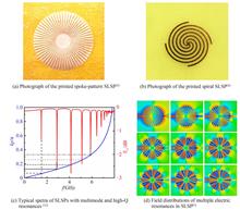
Tianshuo BAI, Wanzhu WANG, Longfei ZHANG, Xuanru ZHANG, and Tiejun CUI
Spoof Localized Surface Plasmons (SLSPs) are electromagnetic resonance modes in the microwave, millimeter-wave, and terahertz frequency bands, which can mimic the modal profiles and physical properties of optical localized surface plasmons based on plasmonic metamaterials. Due to the lower metal loss in these frequencies and the flexibilities in metamaterial designs, SLSPs can achieve excellent sensing characteristics such as deep-subwavelength field confinements, high quality factors, and high dielectric sensitivity. The SLSP concept was theoretically proposed by Pendry and Garcia-Vidal et al in 2012. In 2014, Cui et al proved that SLSPs can be sustained by ultrathin metal patterns on printed circuit boards, and envisioned SLSPs' applications in both the printed circuits and the integrated circuits. Meanwhile, the SLSPs can be integrated with passive and active lumped devices, and exhibit high flexibilities in integration with the signal detection circuits and the wireless communication circuits. Therefore, SLSPs present promising application potentials in compact and portable sensing systems for the internet of things.This paper reviews the representative progress in recent years in the SLSP sensing area. In the first section, some novel resonance modes and resonance structures are introduced, with discussions on their promotions in the sensing indices. Hot topics such as plasmonic skyrmions, exceptional points, quasi-bound states in the continuum, and vortex mode are discussed here. Those novel SLSP electromagnetic modes provide new ideas for sensing. The spiral phase wavefronts of vortex waves can provide rich information and result in a high ability to detect multiple physical quantities. Novel resonance structures including fan-shaped ones, the three-dimensional ones based on origami metamaterials are introduced too, which provide new ideas and methods for SLSP sensor design. The resonance characteristics of SLSP in the terahertz band and its applications are also overviewed. Besides the widely studied array structures under space-wave excitation, it is an irresistible trend to develop terahertz sensing in semiconductor integrated circuits. SLSP sensors pioneers the way for the development of on-chip terahertz biosensing systems. In the second section, the sensing enhancement techniques based on mode coupling and active amplifiers are discussed. Hot spot structures where electromagnetic energy converges can be constructed based on mode coupling inside SLSPs, and can result in highly sensitive hybridization modes. Loading active amplifiers can effectively compensate for the losses in the sensing structure and can improve the quality factor and the excitation efficiency. These techniques supply reliable solutions for the improvements of SLSP sensing indices. Then, typical application scenarios of SLSP sensing are introduced, ranging from solution concentration sensing, bacteria and cancer cell sensing, and mechanical sensing based on flexible SLSP circuits. SLSP can compress the microwave electromagnetic resonances into a deep sub-wavelength scale, greatly enhance the sensing sensitivity to tiny biomedical targets, and break the bottleneck of microwave resonance sensing limited by long wavelengths. Finally, we introduce a recently reported SLSP sensing system, which integrates the SLSP sensor with its signal detection circuits and the Bluetooth module into an ultra-compact size of 1.8 cm×1.2 cm. The signal-noise ratio of this ultracompact sensing system can reach a high value of 69 dB and the system is validated by explosive acetone vapor sensing.The review paper ends with prospective discussions of the SLSP sensing development. Novel principles and phenomena still emerge continuously in the SLSP area, while ultra-compact sensing systems have been constructed yet. We believe that it is good timing now to land the SLSP concept on practical applications. In the following research, there is still a large space for both scientific research and application explorations of SLSP sensing. The mutual promotion of scientific and engineering investigations will surely stimulate the continuous development of SLSP sensing.
Oct. 25, 2023Vol. 52 Issue 10 1052401 (2023)
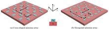
Hengliang ZHU, Fang SONG, Xinyu ZHANG, Chuantao ZHENG, and Yiding WANG
Infrared spectroscopy is widely studied and applied due to its label-free and accurate molecular identification capabilities. However, the small absorption cross-section of the molecule limits its sensitivity. To overcome this problem, the surface-enhanced absorption effect of metal nanoantennas is used to increase the sensitivity when detecting trace target molecules. In the design optimization of metal nanoantenna arrays, silver (Ag) is often used as an alternative to gold (Au) due to its similar properties and lower price. Although much progress has been made in the study of antenna structures, these structures are generally smaller in size, generally less than 100 nm. Relying on advanced technology, the preparation cost is expensive. In this paper, Ag and ultraviolet exposure techniques are used to realize low-cost, large-area metasurface design.First, to study the impact of nanorod size and guide experiments, hollow cross-shaped antenna arrays and hexagonal antenna arrays metasurface are simulated with the help of FDTD software. The simulation results show that the hollow cross-shaped nanoantennas has an extinction peak at 547.7 cm-1, and its extinction coefficient is 64.8%. The extinction coefficient of the hexagonal nanoantennas at 448.3 cm-1 is 85.5%. Compared with hollow cross-shaped nanoantennas, hexagonal nanoantennas have a redshift in resonant wavelength and a larger extinction coefficient. The parameters of length and width of the hollow cross-shaped and hexagonal antennas are swept separately. For hollow cross-shaped nanoantennas, with the increase of length, the formant is significantly redshifted, and with the increase of width, the formant is slightly blue-shifted. For hexagonal nanoantennas, with the increase of length, the formant is significantly redshifted, and with the increase of width, the formant is slightly redshifted. The influence of length on the position of the formant is much greater than the effect of width. The electric field enhancement of the two antenna structures at 547.7 cm-1 and 448.3 cm-1 is 576 and 1 335, respectively. Hot spots are distributed near the edge of the antenna element, especially at the tip. This indicates that the electric field is significantly enhanced around the edge of the metal antennas.Then, the two optimized patterns of metasurface are prepared. To characterize their shape, the substrates are observed with scanning electron microscope. The result shows that the tip of the deposited metal is relatively rounded and not strictly rectangular, which will lead to a decrease in the electric field enhancement of the tip. The Ag nanorod unit is larger in size (error less than 1 μm) relative to the theoretically designed nanorod cell. Compared with the size of the nanorod unit with the hollow cross-shaped structure, the nanorod cell size of the hexagonal structure is smaller. Antenna size is related to the resolution of the lithography machine, the shape of the structure and other factors.To measure the position and shape of the extinction peaks, the transmission spectra of the prepared substrates are measured with a Fourier transform infrared spectrometer. The results show that the hollow cross-shaped antenna substrate has an extinction peak at 525 cm-1, and the extinction coefficient is about 20%. The extinction peak of the hexagonal antenna is located at 474.4 cm-1, and its extinction coefficient is about 24.5%. The extinction coefficient of both structures is smaller than that of the two structures in the simulation, which is caused by the excessive deviation in the transmittance of the silicon used in the experiment and simulation. Compared with the simulation of the extinction peak of the hollow cross-shaped antenna, the extinction peak shows a red-shift of 22 cm-1. And the extinction peak of the hexagonal antenna shows a blue-shift of 26 cm-1 compared with the simulation result. This is due to the fact that the size of the antenna element structure in the prepared substrate deviates from the theoretical design.To verify the performance of designed silver antenna arrays for polymer sensing, Polymethyl Methacrylate (PMMA) was chosen as the analyte. The enhanced absorption effect of hexagonal Ag-Surface-Enhanced Infrared Absorption (Ag-SEIRA) substrate is studied. Both the silicon and hexagonal Ag-SEIRA substrates coated with PMMA have extinction peaks at an absorption peak of PMMA (483.14 cm-1). The extinction coefficients are 3.15% and 8.99%, respectively. The hexagonal antenna arrays achieve 2.85-fold enhancement in PMMA absorption with an enhancement factor of 1995.
Oct. 25, 2023Vol. 52 Issue 10 1052402 (2023)
Shuman LIU, Jinchuan ZHANG, Xiaoling YE, Junqi LIU, Lijun WANG, Ning ZHUO, Shenqiang ZHAI, Yuan LI, and Fengqi LIU
Interband Cascade Laser (ICL) and Quantum Cascade Laser (QCL) are currently the mainstream mid-infrared semiconductor coherent light sources. Among them, QCL has the advantage of watt-level high power in the spectral band above 4 μm, and the power consumption is usually high. ICLs are characterized by low power consumption and operate in the 3~5 μm spectral band. This band contains a wealth of molecular fundamental modes, such as alkane molecules, which are important in the petrochemical industry, SO2 and formaldehyde, which are closely related to environmental pollution, as well as NO and H2S, which are biomarkers in the medical and health fields. At present, most of the high-sensitivity optical sensing systems based on mid-infrared laser absorption spectroscopy technology ranging from 10-6 to 10-9 use single-mode ICLs with low power consumption as the coherent light sources.It is known that one-dimensional Distributed Feedback (DFB) gratings buried near the active region are most commonly used in mode selection for InP-based semiconductor lasers thanks to the mature InP regrowth technology. However, it is hard to regrow the antimonide superlattice waveguide structure of an ICL on a grating layer, which makes the buried grating structure impossible for a DFB ICL. Even for the simplest surface gratings, since an ICL epitaxial structure is usually capped with a thin lattice mismatched InAs layer, the surface grating can only be etched in the InAs/AlSb superlattice waveguide layer. The etching rate of InAs and AlSb is different, resulting in non-smooth grating side walls. As a result, several grating schemes have been reported so far. For example, a high refractive index Ge layer was deposited on the surface of the ICL structure to avoid etching the grating in the superlattice waveguide, where a 1st DFB grating was fabricated by electron-beam lithography and lift-off. In such a process, it should be noted that the Ge layer is relatively easy to fall off. In contrast to the non-crystalline Ge layer, another surface DFB grating ICL was reported recently, in which a 200-nm-thick epitaxial GaSb top layer was used as the grating layer. Etching the grating in the GaSb layer avoids the problem of non-uniform etching rates of InAs and AlSb, which can improve the grating quality.So far, the highest room temperature continuous wave power of 55 mW was achieved by the fourth-order DFB ICLs, in which the gratings were fabricated by dry etch on both side walls of the laser ridge. The process of etching the grating with a high aspect ratio is a great challenge. In addition, the Side-Mode Suppression Ratios (SMSRs) of single-mode emission are low. Recently, DFB ICLs with two sets of gratings were reported, in which a top 1st sampling grating realized single-mode emission and high-order side-wall gratings suppressed the high-order horizontal mode. The laser exhibited a high output power and high SMSRs. From the point of view of processing, the yield of lateral metal gratings placed on both sides of the laser ridge is relatively high. Nanoplus offers lateral metal grating DFB ICLs emitting at a wide wavelength range with low threshold currents and low output power of several milliwatts.In this review we compare and analyze the performance of several DFB ICLs with different grating configurations, and discuss the dominant loss mechanisms and the improvement routes. In addition, vertical cavity surface emission and photonic crystal ICLs are also introduced. Their performances are compared to the DFB ICLs. Although the performance of these two kinds of single-mode ICLs is not satisfactory and cannot be used as a practical single-mode light source at present, their research is still in its infancy, and it is expected that more in-depth research can improve the device's performance in the future.
Oct. 25, 2023Vol. 52 Issue 10 1052403 (2023)
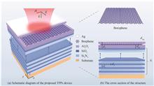
Xiaojian ZHANG, Quan ZHANG, Guilian LAN, Peng LUO, and Wei WEI
Borophene is one of the few 2D materials that is intrinsically metallic with high carrier densities and strong anisotropy, thus offering the unprecedented potential for new generation optoelectronic devices based on 2D materials. Unfortunately, as an unavoidable consequence of the atomic-scale thickness of borophene that is much smaller than the wavelength of operation, the low absorption of monolayer borophene extremely limits the performance of the borophene-based devices and restricts their relevant applications. It is highly desirable to improve the light absorption of borophene to enhance the light-matter interaction, especially in the commercially important telecommunications waveband. A simple and plausible route is offered by optical Tamm Plasmon Polaritons (TPPs) mode, which is an optical state formed between the metal film and one-dimensional photonic crystal. Besides, TPPs are polarization independent and can be generated without the external compensation of wavevector. In general, TPPs could be excited through direct incidence of electromagnetic waves at normal as well as oblique incidence. To this end, we theoretically present a prototype of nearly perfect absorber in borophene enabled by the Tamm plasmon polaritons mode, which achieved by a novel multilayer photonic configuration consisting of a metal film, a spacer, and one-dimensional photonic crystal, and investigated the enhancement of light absorption of monolayer borophene which is positioned within the spacer layer. The monolayer borophene position is optimized based on the nature of field localization in the photonic crystal region. Benefiting from the strong interaction of borophene with the confined field at metal-dielectric interface generating by the Tamm plasmon polaritons mode, the absorption can be enhanced up to 95.53% and 96.62% at the wavelength of 1 550 nm and 1 607 nm along x-direction and y-direction respectively. Then, the transfer-matrix method, an effective approach for the theoretical calculations of light propagation characteristics in the multilayer photonic configurations, is employed to achieve the spectral response in the multilayer structures. The simulated results agree well with the analytical calculations. The proposed absorber shows achieved nearly perfect light absorption is an order of magnitude in optical absorption higher than that of free-standing monolayer borophene, which contributes to the significant enhancement of light-matter interaction. It is also found that the operating resonant wavelength and height of sharp absorption peak could be effectively adjusted by altering the electron density of borophene, the period numbers of dielectric grating and the position of borophene in the resonator. The maximum absorption increases accompanying with the wavelength shift of the corresponding absorption peak when the electron density increases increasingly. The enhancement of the absorption is caused by the increasing imaginary part of the effective permittivity and the slight blueshift of the peak wavelength is caused by the real part of the effective permittivity. Meanwhile, we find that the thicknesses of Si3N4 and SiO2 layers in the one-dimensional photonic crystal also play crucial role in the absorption for the borophene layer. The absorption peak possesses a nearly linear redshift with an increasing of the Si3N4 thickness and SiO2 thickness. In addition, we investigate the dependence of the light absorption in monolayer borophene on the light incident angle. The maximum absorption can be dynamically tuned by adjusting the incident angle and the wavelength of the absorption peak exhibits a blueshift with the increase of the incident angle. These results can offer a promising way for the tunability and selectivity of the enhancement of light-matter interaction in 2D materials. The proposed infrared borophene absorber based on Tamm plasmon polaritons exhibits excellent performance including flexible tunability and high absorption, which is expected to be utilized in a wide range of potential applications in optical communication, photodetection and imaging system.
Oct. 25, 2023Vol. 52 Issue 10 1052404 (2023)
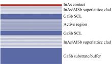
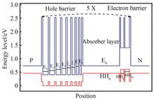
Ting XUE, Jianliang HUANG, Shaolong YAN, Yanhua ZHANG, and Wenquan MA
To reduce the cryogenic cooling cost for high operating temperature applications, the dark current of infrared photodetectors need to be further reduced. Many methods have been proposed such as inserting unipolar-barrier, complementary barriers, the M-structure, and double heterostructures. The Interband Cascade Infrared Photodetectors (ICIP), originally arising from the interband cascade laser, has also been tried. The ICIP structure consists of high bandgap AlSb material, which can further reduce the dark current. Therefore, these features may make high temperature operation possible for ICIPs, especially for the mid wavelength range.This work investigates the ICIP for mid wavelength operation. The ICIP is designed as a p-i-n type. Specifically, the i region is composed of a 5-stage interband cascade structure. Each cascade stage consists of an electron-barrier (eB) layer, an absorber layer, and a hole-barrier (hB) layer, and this sequence repeats five times. The photogenerated electrons in one absorber layer should first pass through the hB layer by optical phonon assisted stepwise transport. The carriers, which arrive at the hole states of the eB layer, finally tunnel to the next absorber layer. Consequently, the energy levels of the eB and the hB layer should be equidistributed. In other words, the energy difference between adjacent levels should be comparable to the optical phonon energy, about 30 meV.The absorber layer of each period is designed as 0.5 μm thick InAs (2.4 nm)/GaSb (3.6 nm) SLs, which has an expected cut-off wavelength of around 4.28 μm. The hB layer is made up of 8 InAs QWs, separated by AlSb barrier layers. For the eB layer, it consists of AlSb(2.1 nm)/GaSb(5.3 nm)/AlSb(2.1 nm)/GaSb(7.5 nm)/AlSb(2.1 nm). The calculated energy separation between adjacent levels is close to the optical phonon energy. The sample is grown on an n-type GaSb (001) substrate by molecular beam epitaxy. After the growth, an array mesa was formed using standard photolithography and dry-etched.We measured the temperature-dependent dark current to reveal the dark current mechanism of the device. The dark current of the device is dominated by the diffusion current instead of the generation-recombination current for the temperature range between 180 K and 300 K, as seen from the Arrhenius plot. The spectral responsivity is measured by calibrating the photocurrent spectrum with the blackbody response with the blackbody source temperature set at 800 K. We calculated the detectivity of the device. At 77 K, the 50% cutoff wavelength is 4.02 μm and the detectivity D* is 1.26×1012 cm·Hz1/2/W for the peak wavelength of 3.79 μm at 0 V. At 300 K, the 50% cutoff wavelength is 4.88 μm and the D* is 1.28×109 cm·Hz1/2/W for the peak response wavelength of 4.47 μm at 0 V.We also observed the Negative Difference Resistance (NDR) effect in our device. The NDR effect can be seen in the dark current curves from 77 K to 220 K. The IP (the NDR peak point current) has almost no change while the IV (the NDR valley point current) increases, and therefore the Peak-to-Valley Current Ratio (PVCR) (IP/IV) decreases with increasing temperature. There are two parts of the tunneling process arising from the interband cascade structures: tunneling through the electron barriers and resonant tunneling. As the dark current equation, n(V) has a strong influence on the dark current, which is determined by the product of the density of states NE, and the Fermi-Dirac distribution function fE, and the tunneling probability TE,V. At the valley point, the dark current is mainly caused by the barrier tunneling mechanism. For the barrier tunneling current, the product of the density of states and the Fermi-Dirac distribution function NEfE increases with elevating the temperature. The tunneling probability, TE,V , is exponentially proportional to the energy state. That is to say, the TE,V at a higher energy state is larger than that at a lower energy state. As a result, the IV rises. Meanwhile, the TE,V of the resonant tunneling dark current can be treated as a constant and the NEfE decreases, resulting in a drop of resonant tunneling current. The dark current at the NDR peak point (IP) is caused by the both two tunneling mechanism, leading to an almost constant peak dark current. Correspondingly, an unchanged IP and an increased IV lead to a smaller PVCR for a higher temperature.
Oct. 25, 2023Vol. 52 Issue 10 1052405 (2023)
Chenglong WANG, Jiabao XIE, Ruobin ZHUANG, Haoyang LIN, Leqing LIN, Ruyue CUI, Hongpeng WU, Huadan ZHENG, and Lei DONG
The measurement of carbon dioxide plays a very important role in breath diagnostics, monitoring industrial safety, monitoring greenhouse gases, observing industrial chemical reactions, measuring combustion completeness, and avoiding fires. Tunable Diode Laser Absorption Spectroscopy (TDLAS) technology has the advantages of high selectivity, high sensitivity, and strong anti-interference ability. The TDLAS systems with a multi-pass cell increase the minimum detection limit by increasing the length of the absorption path. Increasing the absorption path has strict requirements on the divergence characteristics of the laser, and requires enough space. By designing the multi-pass absorption cell, the requirements on optical beam quality can be reduced. The volume of the system can be compressed, and the spatial resolution of the measurement can be improved. In this paper, a highly-sensitive carbon dioxide gas sensor based on a 2 μm laser diode and a Herriott multi-pass absorption cell is designed. The basic parameters of the Herriott multi-pass absorption cell are calculated by paraxial approximation. The solution includes the incident position and the incident angle of the incident light, and the distance between the two spherical concave mirrors. According to the simulation results, a Herriott type multi-path absorption cell is fabricated. The multi-pass cell can fold the optical path with an optical path length of 2.6 m within a length of 54 mm. The minimum detection limit of the system is related to the absorption line intensity of the selected absorption peak. In order to reduce the cost of the system, a distributed feedback laser diode with a center wavelength of 2.004 μm is used to cover the strong absorption line of carbon dioxide molecules at 4 989.9 cm-1. The second harmonic signal with zero background noise at the detection frequency can be detected by 2f- wavelength modulation spectroscopy technology. This technique effectively reduces the noise of the system. The signal measured by the system has white noise, and the method of signal averaging requires a long measurement time. A self-programming real-time Kalman filtering technology on the software level helps to improve the anti-interference ability of the system. Interference by background white noise and abrupt changes to the signal can be avoided. The experimental results show that with the developed TDLAS sensor, the minimum detection limit for carbon dioxide can reach 0.18×10⁻⁶ with an integration time of 1 s. After the self-programmed real-time Kalman filter, the minimum detection limit can be further improved to 0.13×10⁻⁶, resulting in an increase of ~30%. The TDLAS sensor was used to continuously monitor the indoor carbon dioxide concentration for 8 h. An outdoor 24 h continuous monitoring for carbon dioxide concentration on the building roof of Jinan University. This work demonstrates the stability and robustness of the developed TDLAS sensor. The sensor can respond in real time to changes of carbon dioxide concentration in the ambient air. The real-time Kalman filter carried by the system has better stability, which can effectively improve the minimum detection limit of the system.The optical multi-pass can be accurately designed by the method of paraxial and non-paraxial approximation. In the next work, a dense multi-pass absorption cell can be designed to fold longer optical paths between the same two mirror. However, the light spot of the dense multi-pass absorption cell will become irregular with the increase of the number of reflections. In this case, the incident hole and exit hole of the cell need to be manufactured with higher precision. If the multi-passed light cannot pass through the exit hole completely, the interference of the absorption cell will increase resulting in a decrease in signal to noise ratio. The Herriott multi-path absorption cell can avoid this problem very well.
Oct. 25, 2023Vol. 52 Issue 10 1052406 (2023)

Yuechong SHI, Yafei LI, Fang SONG, Chuantao ZHENG, and Yiding WANG
At present, the demand for gas sensors is moving towards miniaturization, low power consumption and networking. Among them, laser absorption spectroscopy has wide application prospects in related fields with advantages of fast detection speed, high accuracy, good stability, and long service life. However, the commonly used laser gas sensor system is generally large in size, high in power consumption and high in cost, which is difficult to be widely used as a gas sensor node. Therefore, it is urgent to develop a new spectroscopy gas sensing system with small volume, low power consumption and low cost to promote the application of laser gas sensing technology in “carbon neutralization”.Based on the above social needs, we developed a hardware reconfigurable Wavelength Modulation Spectroscopy (WMS) methane sensor. Based on the characteristics of Field Programmable Gate Array (FPGA) hardware algorithm acceleration, the hardware-based wavelength modulation gas absorption spectroscopy analysis algorithm, realizes quasi-synchronous output of scan signal and harmonic signal amplitude as well as on-chip integration of WMS with a delay time of only 4.05 ms. The on-chip logic circuit is mainly divided into WMS analysis module and WMS drive signal generation module. Based on Direct Digital Synthesis (DDS) technology, the WMS drive signal generation module is used to generate sine wave and triangular wave signals required by WMS, and both signal frequency and phase can be tuned in a wide range, which can flexibly control the sensor operation according to an enabling signal. The core of WMS analysis module is an orthogonal phase-locked amplifier. This work focuses on enhancing the hardware reconfigurability to enhance the flexibility of the sensor system. Only when the enabling signal is in high level, the WMS analysis module and the drive signal generation module start to work, which lays the foundation for intermittent work, scanning signal alignment, and gas absorption fixed point analysis. The feasibility of the intermittent work is verified by the actual measurement. The system has a unified sampling clock, and an on-chip clock generation unit based on external reference signals is constructed. On the basis of avoiding the frequency offset problem, the flexible reconstruction of the system sampling clock is realized. A standard orthogonal signal generation module based on DDS technology is established to realize the generation of standard orthogonal signals at any frequency. Combined with the characteristics of finite impulse response filter that the frequency response can be reconstructed by modifying parameters, the phase-locked analysis at any target frequency is realized. The on-chip system logic part is developed in hardware logic language as a whole, and there is no problem of “program runaway”. After the design of the system logic part, the software simulation is carried out to verify the accuracy of the system logic function. In order to verify the linearity of harmonic signal extraction of the designed hardware reconfigurable wavelength modulation methane sensor, a sinewave verification experiment is carried out. By analyzing the amplitude extraction results of different standard sinewave signals, a step output of the system under different inputs is observed, and a linear response with a goodness of fit of 99.99% is obtained. The measured sinewave amplitude fluctuation range is about ±0.5 mV. In order to verify the actual sensing performance of the methane sensor, methane experiments are carried out using a Herriot gas cell with an optical path length of 25 m and a laser with a central wavelength of 2 334 nm for targeting the absorption line of methane at 4 284.5 cm-1. It can be seen from the experimental results that the gas detection linearity of the methane sensor is 99.97%. The stability analysis shows that the sensor resolution is better than 25 parts-per-million in volume (ppmv), and the response time is ~ 4.9 s. In addition, the Allan variance results show that when the integration time is 0.5 s, the detection limit of the sensor is 7.8 ppmv. Methane leakage test is carried out. Through the analysis of the measured CH4 concentration levels when CH4 leakage occurs, the detection ability of the sensor for methane leakage is proved. Compared with the existing methane sensor based on software architecture, the extremely low data delay lays a foundation for intermittent work, and provides the possibility to realize the application of node-type low-power gas detection. At the same time, the sensor has high accuracy, fast response speed, and can be used flexibly and conveniently based on actual needs. The developed sensor shows a good application prospect with high electronic integration based on FPGA.
Oct. 25, 2023Vol. 52 Issue 10 1052407 (2023)
Xiaoqiang SU, Yucong HUANG, Shaoxian LI, Ge SONG, and Quan XU
Spoof Surface Plasmon Polaritons (SSPPs) are a surface electromagnetic modes of the low-frequency regime with characteristics similar to those of surface plasmons in the optical regime. By altering the geometric parameters of the metal structure, the localized electromagnetic field can be manipulated, enabling its significant role in various fields such as on-chip communication, signal processing, and sensing detection. Herein, we propose a novel strategy to achieve the refractive index sensor on chip. The classical two-side metallic stripes are utilized as SSPP waveguide, and two types of meta-particles with diverse Q-factors and identical resonant frequencies are employed as a bright-dark module along the propagating trajectory of the waveguide structure. Due to the near-field interactions between resonant modes of meta-particles and the evanescent field of waveguide, Electromagnetically Induced Transparency (EIT) effect is achieved on planar SSPP waveguide. The working frequency is 6.03 GHz and Q-factors can be up to 28.575. Due to the characteristics of the electric-field distribution at the EIT-like peak frequency, a compact refractive-index sensor on-chip is developed. The sensing mechanism of the on-chip EIT-like effect primarily relies on the sensitivity of the strongly confined electric-field inside the dark mode resonators to the refractive-index of surrounding medium. This sensitivity can be reflected into the shift of the EIT-like characteristic frequency and changes in the resonance amplitude. The circular analyte is chosen as the study object and positioned above the center of the dark mode resonators. The full-wave simulations are conducted to investigate the response characteristics of the EIT transparency window to variations in parameters such as the refractive index n, tangent loss tan σ, thickness th, and radius r of the analytes. The increase of refractive index n contributes to redshift of EIT window, which show the linear relationship and the slope is described as the sensitivity of sensor on-chip. As the thickness th and radius r of the analytes increase, the relationship between redshift and refractive index still maintains a linear trend. The simulated results have shown that the on-chip sensor exhibits maximum sensitivity of 1.12 GHz/RIU within the refractive index range from 1.26 to 1.79 (corresponding to dielectric constants in the real part of 1.6 to 3.2), and th=1.0 mm, tan σ=0, r=1.5 mm, respectively. Correspondingly, the Figure of Merit (FOM) value is calculated to be 5.45. To experimentally validate the proposed on-chip sensor based on the EIT-like effect, the SSPP device is fabricated using the process of printed circuit board, and sensing measurements are performed on three types of edible oils, including linseed oil, sunflower oil and flaxseed oil. Three types of edible oils differ mostly owing to their fat contents, which causes a variation in the related refractive index. Use a syringe with a needle to drop each edible oil to the position of the center of the dark mode resonators, the results have confirmed that the sensor exhibits high sensitivity, label-free detection capability, and experimental flexibility. As the parameters of analytes are th=0.6 mm, r=1.5 mm, tan σ=0, n=1.52, 1.50, and 1.49 in the simulation, the simulated results agree well with the experimental results. The proposed on-chip sensor based on the EIT-like effect in SSPP waveguide possesses several key characteristics, including simple structural design, easy integration, and high sensing sensitivity. Extendedly, by placing EIT-like modules with different characteristic frequencies along the SSPP waveguide, simultaneous sensing detection of multiple analytes will be achieved. This approach provides a novel perspective for the design of on-chip sensing devices.
Oct. 25, 2023Vol. 52 Issue 10 1052408 (2023)
Binru ZHOU, Yu MA, Shichen ZHANG, Fengqi LIU, and Quanyong LU
Mid-infrared to terahertz spectral regions (3~300 μm) are of particular interest to sensing and monitoring since a large number of gases such as CO, CH4, NH3, SO2, HCl, etc., has strong characteristic vibrational transitions. These molecular fingerprints enables fast and pricise detection when a high power laser and a sensitive detector is applied. A morden sensing system normally includes a separate laser, a detector, and a gas chamber, which makes the system rather bulky and expensive. A chip-based sensing system on the other hand, with all the components integrated on a single chip, will greatly reduce the size, weight, power, and cost of the system. Currently, there are limited light source candidates for mid-infrared and terahertz sprectral bands. Devices that can generate light sources in the infrared band include: quantum well lasers, solid-state laser-pumped optical parametric oscillators, interband cascade lasers, and quantum cascade lasers. As a conventional semiconductor laser light source, quantum well laser is based on the optical transition between the conduction band electrons and valence band holes in the quantum wells, its emitting wavelength is determined by the band gap of the semiconductor quantum material. The photon energy in the mid- and far-infrared bands ranges from 0.04~0.4 eV, which is much smaller than the bandgap of the majority of quantum well laser materials themselves. It is difficult for traditional quantum well lasers to cover the mid- and far-infrared as well as terahertz bands. Devices using solid-state laser-pumped optical parametric oscillators to generate the mid- and far-infrared emission are generally large in size and low in efficiency, and have limitations in practical applications. In addition, based on cascade transition between the conduction band and the valence band, interband cascade lasers can cover the 3~6 μm band. These type of laser is of much lower threshold current density and threshold power density. However, for the mid-infrared and even further wavelength bands, the performance of interband cascade lasers shows a decreasing trend. Based on intersubband transition in the conduction bands, Quantum Cascade Laser (QCL) is a new type of semiconductor laser source with high responsivity, high nonlinearity, and wide spectral coverage from mid-infrared to terahertz band. Compared with other laser sources that can produce mid-infrared sources, quantum cascade lasers have the advantages of small size, high energy efficiency, and wider wavelength tunability, and their wavelength ranges have been extended to the 3~25 μm and 1~6 THz bands, which make them the most promising laser light sources in the mid-infrared band.In recent years, quantum cascade lasers have important applications in the fields of long-range hazardous and explosive detection, biomedicine, infrared countermeasures and long-range free-space optical communications. Since the sensitivity and detecting range are proportional to the output power of the lasers, further improvement of the output power and electro-optical conversion efficiency of the devices is one of the most important goals of QCL research. By improving the device structure design, material epitaxial growth technology, and device preparation process, the output power, electro-optical conversion efficiency, beam quality, threshold current density, and other key parameters of quantum cascade lasers have been continuously optimized. In addition, broadly tuned, single-mode quantum cascade lasers with high side-mode suppression ratio have also become a research hotspot due to their urgent needs in gas sensing, spectroscopic measurements and other fields. Further, difference-frequency generation terahertz light sources and on-chip sensing technologies based on quantum cascade lasers are attracting more and more attention for the potential applications.With the recent rapid development in output power and wall-plug efficiency, QCL is becoming the most promising laser source in mid-IR and THz regions. The high power characteristic together with the strong absorption at zero bias makes QCL the ideal platform for on-chip sensing. This paper focuses on the recent development mid-infrared quantum cascade lasers and their application in on-chip sensing. Firstly, the history and working principle of quantum cascade lasers is introduced. Subsequently, the research progress of mid-infrared quantum cascade lasers in wall-plug efficiency, output power, wavelength tunability, single-mode operation, optical frequency comb, THz difference-frequency generation are summarized and their application in on-chip sensing are also discussed.
Oct. 25, 2023Vol. 52 Issue 10 1052409 (2023)
Yulin DU, Xinrong XIE, Hongsheng CHEN, and Fei GAO
Photoconductive Antenna (PCA) is the most common optoelectronic Terahertz (THz) source for the widely used THz Time-Domain Spectroscopy (THz-TDS) and imaging technique. But its application is still hindered by low output efficiency which originates from two issues, including low photon-electron conversion efficiency, and low vertical directivity resulting from the horizontal leakage, i.e., propagating transmission line modes along the electrode pair of the PCA. However, current research can only achieve insufficient improvement in output efficiency since they are limited to solving the two issues separately. Here the hierarchical spoof plasmonic structures are proposed to enhance THz-PCA. Hierarchical structures combine the metallic nanoblock array and microscale Spoof Surface Plasmon Polariton (SSPP) periodic gratings together to solve the two issues simultaneously and increase the THz radiation output power. The PCA we proposed adopt a Bottom-Located Thin-Film (BLTF) structure where golden electrodes are sandwiched between a Low-Temperature-grown Gallium Arsenide (LT-GaAs) substrate and a Si lens, and the hierarchical structure includes a golden nanoblock array set above the substrate and periodic teeth pairs integrated between electrodes.The improvement of conversion efficiency by nanoscale plasmonic structure is analyzed first. The nanoblock array is elaborately designed so that the Spoof Localized Surface Plasmon Resonance (SLSPR) is excited under laser irradiation, and leads to electric field enhancement around the structure. A three-dimensional multi-physical simulation is conducted using COMSOL. The simulation results show that a nanoblock array brings about significant electric field enhancements inside the substrate under nanoblocks compared to that without nanoscale structure. Specifically, the volume average electric field amplitude of the substrate increases by about 1.52 times. The photocurrent is simulated further and with a nanoblock array, the increasing rate of the peak value reaches around 47%.Then the vertical directivity enhancement brought by the microscale SSPP structure is validated. When the frequency falls into the bandgap of the SSPP periodic gratings, the first-order SSPP mode is forbidden, and the second-order SSPP mode also cannot be excited efficiently due to the orthogonality between the dipole source pattern and the higher-order SSPP mode, thus suppressing the horizontal radiation leakage in the operating frequency range. Simulations conducted in CST Studio verify that the electromagnetic field propagates freely to the ends of bare electrodes (without SSPP periodic gratings), while on SSPP-modified electrodes, lateral propagation is almost blocked, and take the radiation power pattern at 1.01 THz as an example, the horizontal directivity decreases by 3 dB, accompanied by the increase of the vertical directivity.Finally, the joint effect of hierarchical structures is investigated. As it is difficult to establish a trans-dimensional and multi-physical co-simulation, so a mathematical method is adopted to obtain the enhanced performance of the PCA with the hierarchical structures by connecting the results of the nanoscale and microscale structures. The electrodes and lens compose a linear system where the output is the product of the input photocurrent and its spectral response and is proportional to the input photocurrent. By multiplying Fourier coefficients of the ordinary and nanoblock-enhanced photocurrents by corresponding frequency responses of the regular and SSPP-integrated antennas at the same frequency, the vertical radiation power density spectra of PCAs under different circumstances are achieved. The PCA with the hierarchical plasmonic structures is better than those with two schemes separately, which shows a huge increasement in vertical radiation power density in a relatively broad operating band from 0.86 to 1.51 THz compared with the PCA without hierarchical structures. And the far-field power patterns quantitatively illustrate that at 1.27 THz, in the circumstance of the same input laser, radiation power density experiences a growth of 4.77 dB, confirming that hierarchical spoof plasmonic structures bring great improvements in the photon-electron conversion efficiency and vertical directivity of the THz-PCA.
Oct. 25, 2023Vol. 52 Issue 10 1052410 (2023)
Wenjing WU, and Liang PENG
In the traditional Split Ring Resonator (SRR) -based microwave microstrip sensor, the microstrip line is coupled with SRR, and the mantic coupling is appeared between microstrip line and SRR. The electrical filed is distributed at the gap of SRR. A high resonant frequency is occurred due to the relatively low equivalent capacitance. And, the traditional SRR-based sensor shows a low sensitivity. In order to improve the detection sensitivity, an Interdigital Capacitance Structure (ICS) is inserted into the opening of the split ring resonator to enhance the density of electric field. From the simulated distribution of electrical field, it can be seen that more electrical field is concentrated at the slot of interdigital capacitance with comparison to traditional SRR-based sensor. The meander slot can increase the interacted path of electrical field, create a higher equivalent capacitance, so more electrical field is focused on the slot of interdigital capacitance. As known, the external environmental factors, such as temperature, humidity, gas pressure, etc, can cause an influence on the measured results and result in a large measurement error. In order to suppress the interferences of external environment, a differential structure is added. With comparison to traditional microstrip sensors, the proposed differential microwave sensor can overcome low sensitivity and effects of environment factors. The designed differential structure adopts the form of two split ring resonators distributed on both sides of a single microstrip line, and the microstrip line is coupled with the two split-ring resonators, and the magnetic couplings distributed on both sides are equal. An equivalent circuit model is adopted to analyze the operating principle of proposed microwave sensor, the element values of equivalent circuit model are calculated, then Keysight ADS is adopted to fine-tune all the element values to match the simulation results. It can be found that there is a good agreement between them. The consistent also reveals the correctness of proposed equivalent circuit model. Besides, mathematical analysis is utilized to explain the phenomenon that the ICS-SRR has a higher confined electrical field than traditional SRR. Then, simulation and experimental results both verify the correctness of theoretical analysis. In the experiment, one resonator serves as the reference unit and the other resonator serves as the measurement unit. The liquid under test is placed at the test resonator. In measurement, the water-ethanol mixtures with water concentrations changing from 0% to 100% with a step of 20% are adopted to establish the mathematical model. As the mixture solutions of water-ethanol with different volume fractions of water are injected, the resonance frequency of the measurement unit will show significant frequency shift and notch amplitude deviation compared to the reference unit. The deviations of resonant frequency and notched magnitude can be used to fit the complex permittivity. Then, in order to demonstrate the correctness of established mathematical model, the water-ethanol mixtures with water concentrations altering from 10% to 90% with a step of 20% are utilized. By substituting the measured resonant frequencies and notched magnitudes for water-ethanol mixtures with water concentrations changing from 10% to 90% into the established mathematical model, the real and imaginary parts of complex permittivity for water-ethanol mixtures with water concentration changing from 10% to 90% can be obtained. The experimental results show that the average sensitivity of per unit volume of the proposed sensor can reach 3.630 8%/μL, which is several times higher than the other designs. In addition, the proposed microwave sensor can also be adopted to measure other binary mixed solutions by establishing the corresponding mathematical models.
Oct. 25, 2023Vol. 52 Issue 10 1052411 (2023)
Kuiwen XU, Shasha HOU, Haoqian DENG, Jiangtao SU, and Wenjun LI
Currently, there are two primary approaches to addressing nonlinear electromagnetic inverse scattering problems. One method involves linearizing these issues, while the other treats them as iterative optimization problems. However, a significant challenge arises in real-world applications, where achieving uniform antenna coverage around the target proves to be exceptionally difficult. To surmount this challenge, limited aperture imaging methods have been proposed. Although limited aperture imaging provides more significant flexibility, it amplifies the nonlinearity of electromagnetic inverse scattering problems, resulting in relatively limited research on this front.This paper introduces a novel method founded on the limited aperture Rytov integral approximation for the purpose of quantitative inversion imaging of high relative permittivity and large-sized target objects. That is, the antennas are distributed only on one side of the region of interest or on some specific angles; limited aperture imaging provides greater flexibility. To begin, we introduce the concept of the phaseless Rytov approximation and meticulously analyze the complex refractive index within low-loss media. By analyzing the reflection and transmission of the incident field from the free space to the lossy media, the concept of effective refractive index is introduced and combined with Snell's theorem to solve the relationship between the effective refractive index and the actual refractive index, and the relationship between the actual refractive index and the dielectric constant is established according to the relationship between the dielectric constant and the refractive index in the low-loss media. Under the conditions of high frequency and low loss, we estimate the contrast function by taking into account the interplay between the effective refractive index, the actual refractive index, and the dielectric constant. We then employ mathematical corrections to approximate the scattered field and its gradient within the scattering object, thereby enhancing the traditional Rytov approximation. This enhancement results in the development of a phaseless limited aperture Rytov integral approximation model.In the simulation section, three different scattering objects with varying strengths are selected, namely weak scatterers, medium scatterers, and strong scatterers. This model is capable of providing quantitatively better reconstruction results for weak and medium scatterers with different shapes, characterized by high permittivity and large target size. For strong scatterers, it accurately reconstructs the target shape by considering the imaginary component of the contrast function. Additionally, for multi-target scenarios, both medium and strong scatterers are well-reconstructed in terms of object shapes. Furthermore, the model also yields favorable results when altering the operating frequency and antenna placement layout. Lastly, this model exhibits strong noise resistance capabilities.The proposed method is expected to be widely used in medical imaging, non-destructive testing and ground penetrating radar.
Oct. 25, 2023Vol. 52 Issue 10 1052412 (2023)
Yihao WU, Xuehua XIAO, Ran BI, Yadan LI, Chuantao ZHENG, and Yiding WANG
Infrared transparent conductive thin film is a special material that can both transmit light and conduct electricity. It is widely used in solar cells, radiative cooling, infrared detector anti-interference coating, transparent electrode, sensing technology, photoelectric devices and other fields. Bismuth telluride is a semiconductor material with a molecular formula of Bi2Te3, which has good conductivity and a band gap width of 0.145 eV at room temperature. Based on the excellent optoelectronic properties of Bi2Te3 materials and their significant research value in the field of broadband photodetectors, Bi2Te3 is one of the ideal candidate materials in the field of infrared transparent conductive films.The preparation methods of Bi2Te3 films usually include pulsed laser deposition, magnetron sputtering, physical vapor transport, vacuum evaporation, molecular-beam epitaxy, electron beam deposition, etc. In this paper, Bi2Te3 thin films are deposited on fused silicas substrates and zinc selenide substrate by magnetron sputtering. The structure, composition and morphology of the prepared Bi2Te3 thin films are analyzed by diffractometer, X-ray photoelectron spectrometer and cold field emission scanning electron microscope. The optical transmittance, conductivity, carrier mobility and other optoelectronic properties of the films are studied. The test results show that annealing is conducive to the crystallization of the films, and does not change the preferred orientation of the crystals. The crystallinity is excellent when the annealing temperature is 350 ℃, and the crystallinity will become better with the increase of the film thickness. The Fourier transform infrared spectrum test results show that the optical transmittance of Bi2Te3 films deposited on fused silicas and zinc selenide substrates decreases with the increase of film thickness and annealing temperature. The optical transmittance of the films deposited on zinc selenide substrates is longer than that of fused silicas, and the optical transmittance is more stable. The hall effect test results indicate that with the increase of film thickness and annealing temperature, the resistivity of Bi2Te3 film gradually decreases, and the minimum resistivity of the prepared Bi2Te3 film is 1.448×10⁻³ Ω·cm, with a mobility of 27.400 cm2·V-1·s-1 and a carrier concentration of 1.573×1020 cm-3. The Bi2Te3 thin film deposited on fused silicas substrate has a maximum transmittance of 80% in the 1~5 μm infrared band, with a thickness of 15 nm. After annealing at 200 ℃, the transmittance can reach 60% and the resistivity is 5.663×10⁻³ Ω·cm. The maximum transmittance of Bi2Te3 thin film with thickness of 15 nm deposited on zinc selenide substrate in 2.5~20 μm infrared band reaches 65%, and after annealing at 200 ℃, the transmittance can reach 60%. At this time, the resistivity of the film is 9.919×10⁻³ Ω·cm, with good photoelectric performance.Taking into account the photoelectric performance of the prepared thin film, when the thickness of the Bi2Te3 thin film is 15 nm and the annealing temperature is 200 ℃, the film has the excellent photoelectric comprehensive performance. Bi2Te3 thin films deposited on fused silicas and zinc selenide substrates have good photoelectric properties, which have potential applications in infrared detectors and anti-interference.
Oct. 25, 2023Vol. 52 Issue 10 1052413 (2023)
Xueying WANG, Zhening ZHANG, Mingquan PI, Zihang PENG, Chuantao ZHENG, Fang SONG, Yue YANG, and Yiding WANG
Most gas molecules have vibration characteristic absorption peaks in the mid-infrared spectral range (2.5~20 μm), which can be used for trace gas detection and quantitative analysis. On-chip gas sensing that enables waveguide interconnection can improve system portability. Because quantum cascade laser and quantum cascade detector material structures can be epitaxially grown on the InGaAs-InP platform, it can be used for the preparation of on-chip integrated gas sensors. On the InGaAs-InP platform, the refractive indices of nInGaAs = ~ 3.4 and nInP = ~ 3.1 at λ = 4.602 5 μm are insufficient to realize the total internal reflection constraint between core and substrate. We can etch the InP substrate by using hydrochloric acid so that the refractive index between the core and cladding is approximately 2.4. At this point, the suspension structure allows gas to flow through the upper and lower cladding, allowing stronger interaction between gas molecules and light. In order to study the sensing performance of on-chip waveguide in the mid-infrared band, a suspended photonic crystal waveguide and a suspended ridge waveguide sensor based on InGaAs-InP platform are proposed for targeting the 2 172.75 cm-1 absorption line of carbon monoxide. Based on Lambert-Beer law, Rsoft software and COMSOL software are used to optimize the waveguide structure. The lattice constant, hole radius, central hole radius, ridge width, strip width, ridge height and strip height of the photonic crystal waveguide are optimized, and the performances of the two sensors are calculated.Firstly, a mid-infrared suspended InGaAs-InP photonic crystal waveguide sensor is proposed. The InGaAs photonic crystal waveguide adopts a hexagonal lattice with a lattice constant of a. The width of Holey Photonic Crystal Waveguide (HPCW) is 3a, and the thickness of InGaAs layer hInGaAs is 1.15 μm. The lattice constant, hole radius and central hole radius parameters of the photonic crystal waveguide are optimized by constructing a defect row in the Γ-K direction. The central defect row radius of the constructed waveguide is rs = 0.6r, where r = 0.27a is the aperture radius of the photonic crystal. The relationship between the lattice constant of the photonic crystal waveguide and the group index (ng) is obtained by simulation. When the lattice constant a = 1 018 nm and the photonic crystal waveguide ng is 43.97, the optimal waveguide structure is obtained at λ = 4.602 5 μm. It is found that most of the light is confined to the center hole region, and the peak electric field intensity of the center hole cross-section is increased by ~ 3.41 times. At this time, the power confinement factor fPC of the photonic crystal waveguide is 250.69%, the optimal waveguide length Lopt = 72 μm, and the limit of detection CLoD = 9.13 × 10⁻⁶.Then, a mid-infrared suspended InGaAs-InP ridge waveguide sensor is proposed. The total thickness of the core layer is set to 780 nm. In order to obtain a large fPC under guided mode condition, COMSOL Multiphysics software based on finite element method is used to optimize the waveguide structural parameters, including ridge width w1, plate width w2, ridge height h1, plate thickness h2 and waveguide length L. The optimum waveguide structure and the optical mode field distribution of TM0 mode of the mid-infrared suspended ridge waveguide are obtained. Most of the light is concentrated around the ridge. fPC = 115.65%, Lopt = 162 μm, and CLoD = 8.51 × 10⁻⁶.Comparing the two sensors designed, since HPCW can only guide TE mode, a polarization rotator is required to integrate it with the quantum cascade device with TM polarization. Ridge Waveguide (RWG) can support TM polarized light and does not require a polarization rotator for integration, which reduces total transmission loss and integrated device area, and simplifies the preparation process. The advantage of suspended HPCW is that it has a high group refractive index, so it can effectively reduce the light absorption path length. But HPCW has a higher propagation loss, which is not conducive to improving the sensitivity of integrated gas sensors. The lower propagation loss of the suspended RWG allows for longer waveguide lengths, which in turn improves gas sensor sensitivity. The influence of propagation loss on the performance of the two sensors is analyzed and calculated, and the variation curves of Lopt and CLoD versus αint are obtained. Lopt decreases and CLoD increases with the increase of propagation loss. If the waveguide propagation loss can be effectively reduced, the lower detection limit can be further reduced.With CO as the target gas, the InGaAs-InP platform is used to simulate the design of suspended photonic crystal waveguide and ridge waveguide. The waveguide parameters are optimized to achieve single-mode transmission and higher fPC. After optimization, fPC of the suspended photonic crystal waveguide and ridge waveguide are 250.69% and 115.65%, respectively. When the waveguide loss is 27.5 dB/cm and 3 dB/cm, respectively, the optimum waveguide lengths of the two sensors are determined, respectively. When SNRmin = 10, CLoD of the two sensors are 9.13 × 10⁻⁶ and 8.51 × 10⁻⁶, respectively.
Oct. 25, 2023Vol. 52 Issue 10 1052414 (2023)
Jiatang LIU, Shilei LI, Yanan QI, and Shuai CHEN
Traditional optical devices have certain limitations, due to the diffraction limit, the development of optical devices is limited, making the optical devices bulky and not conducive to miniaturization. Optical devices can transmit and process information within the sub wavelength range, effectively addressing the issue. Metal-dielectric-metal waveguide can regulate the light propagation signal in the subwavelength range, and surface plasmon polariton has the characteristic of breaking the diffraction limit, making it possible to further miniaturize optical devices. Based on surface plasmon polaritons, a waveguide side coupled resonator system with metal baffles is proposed. When incident light enters the structure from the incident end of the waveguide, a narrow discrete band is formed in the resonant cavity, and a metal baffle generates a wider continuous state. When the narrower discrete state interferes with the wider continuous state, two different modes of Fano resonance lines are formed. In this paper, the finite difference time-domain method is used to simulate the transmission characteristics of the structure. The magnetic field distribution, electric field distribution, transmission characteristics, and sensing performance of the structure are studied separately. Based on the magnetic field distribution and electric field distribution, the formation mechanism of Fano resonance can be better explained. According to the analysis of simulation data, the geometric parameters of the structure and the refractive index of the medium can adjust the transmission performance of the structure. The geometric parameters of the structure are optimized. Firstly, when the side length of the Ag square is a=190 nm, the separation distance is k=10 nm, the coupling distance is g=15 nm, and the circular radius R of the structure is parameterized in steps of 10 nm from 270 nm to 330 nm, the quality factors at different R are calculated. Considering the overall quality factors of these two Fano resonances, the optimal value of the circular radius of the structure is taken as 300 nm. Secondly, when the circular radius R=300 nm, the separation distance k=10 nm, the coupling distance g=15 nm, and the Ag square side length a of and the structure is parameterized in steps of 15 nm from 160 nm to 220 nm, the quality factors at different a are calculated. In order to simultaneously consider the quality factors of these two Fano resonances, the optimal Ag square side length a of the structure is set at 190 nm. Thirdly, when the circular radius R=300 nm, the Ag square side length a=190 nm, the coupling distance g=15 nm, and the resolution distance k of the structure is parameterized and scanned in steps of 1 nm from 6 nm to 14 nm, the quality factors at different k are calculated, and the two Fano resonances are combined. Therefore, the optimal resolution distance k of the structure is chosen as 10 nm. Fourthly, when the circular radius R=300 nm, the Ag square side length a=190 nm, the separation distance k=10 nm, and the coupling distance g of the structure is parameterized in steps of 1 nm from 6 nm to 16 nm, the quality factors at different g are calculated. Overall, considering the quality factors of these two Fano resonances, the optimal coupling distance g of the structure is determined to be 10 nm. Under the optimal parameters, the figure of merit of the two Fano resonances FR1 and FR2 generated by this structure are 4.502×10⁵ and 1.967×10⁵, the corresponding sensitivities are 800 nm/RIU and 1 400 nm/RIU, respectively, the quality factor and sensitivity of the two Fano resonances have reached high values, both of which have good sensing performance. The designed coupling structure can provide a feasible way to improve the performance of micro/nano optical sensors.
Oct. 25, 2023Vol. 52 Issue 10 1052415 (2023)
Junhui LI, Hao YAO, Jiayao DENG, and Kaixin CHEN
Grating Assisted Directional Coupler (GADC) is an important optical waveguide device because it is capable of achieving efficient coupling between the two modes having mismatched phase. GADC provides a new way to improve the performances of the coupler and the grating. Due to its compact structure, easy integration, versatility, and good wavelength selectivity, GADC is now widely used in various scenarios, such as codirectional coupler, optical add-drop filter, tunable delay line, wavelength division multiplexer, mode division multiplexer, filter, mode filter, and so on. However, most of these devices do not have tunability, while tunability is the key for improving the device performance, realizing device reconfiguration, and enlarging the device fabrication tolerance. Up to now, the tunability of optical waveguide devices are usually realized based on the Electro-Optic (EO) and the Thermo-Optic (TO) effects. Among them, EO tuning is more fascinating due to its high tuning speed and low power consumption. Lithium Niobite (LN) On Insulator (LNOI), a newly emerging integrated optics platform in recent years, not only keeps the excellent EO, acousto-optic, and nonlinear optical properties of LN, but also enables high-index-contrast and hence high-confinement waveguide, which makes it an excellent platform for developing compact and high-performance EO devices.In this paper, a high-performance electro-optical tunable GADC in LNOI is proposed and demonstrated. Our proposed device consists of an Asymmetric Directional Coupler (ADC), a sidewall Long Period Waveguide Grating (LPWG), and a set of electrodes. The ADC is composed of a Single-Mode Waveguide (SMW) and a Two-Mode Waveguide (TMW), and both are rib waveguides with identical etch depth. The LPWG is formed on the inner side of the ridge of the TMW. Both ADC and the LPWG are formed with the Inductively Coupled Plasma (ICP) process simultaneously. Due to the large birefringence of LN, the LPWG can not meet the phase matching of the two polarized fundamental modes in the SMW and the TMW simultaneously, thus it is designed only for the coupling of the E11Tz and E11Szmodes. To employ the maximum EO coefficient γ33 of LN, a 600-nm thick x-cut LN wafer and y-propagation layout are adopted. And Titanium (Ti) gold electrodes are placed both sides of the TMW to provide EO tuning. Here, to avoid the light absorption induced by the metal electrode, a Silicon Dioxide (SiO2) buffer layer is formed on the LNOI waveguides to isolate the waveguides from the electrodes. In this work, the width of the SMW and the TMW are set to 1.2 μm and 2.0 μm, respectively, the space between them is set to 0.7 μm, and the etch depth is set to 200 nm. With these data, the grating period is 48.0 μm at the resonant wavelength of 1 550 nm and the grating length is 816 μm, corresponding to 17 grating periods, calculated by using the beam propagation method (Rsoft) to simulate the light propagation through the grating when the grating duty cycle is set to 50%.We fabricated dozens of GADCs with somewhat different periods on a single x-cut LNOI chip. When the E11Tzmode is excited in the TMW, the transmission spectrum of the TMW exhibits a distinct rejection band with a maximum contrast of 14.8 dB at the center wavelength 1 595.3 nm, while the output spectrum of the SMW exhibits somewhat complementary pass-band. This indicates that the E11Tz mode of the TMW is coupled into the E11Sz mode of the SMW near the rejection band. In addition, when the E11Szmode is excited in the SMW, the output spectrum of the SMW exhibits a distinct rejection band with an isolation of 13.6 dB at the wavelength of 1 595.3 nm, while the spectrum output from the TMW exhibits a distinct complementary pass-band near the rejection band, indicating an efficient coupling from the E11Sz mode of the SMW to the E11Tzmode of the TMW.To facilitate the investigation of the EO and TO tunability of the device, we further packaged GADC unit on the chip. The two ends of the TMW and the SMW of GADC were pigtailed with 3.2 μm UHNAF fiber arrays (with two fibers) using UV glue. The measured results show that the central wavelength of the rejection band of the TMW transmission spectrum redshifts from 1 595.3 nm to 1 599.0 nm as the tuning voltage increases from 0 V to 10 V, the maximum contrast of 14.8 dB at the center wavelength 1 595.3 nm. While the center wavelength of the rejection band moves from 1 595.3 nm to 1 592.3 nm as the tuning voltage changes from 0 V to -8 V, and the isolation reaches its maximum value of 20.7 dB at -2 V. The EO tuning efficiencies are 0.38 nm/V (1 592.3~1 599.0 nm). Similarly, the center wavelength of the rejection band of the SMW transmission spectrum moves from 1 595.3 nm to 1 597.9 nm as the tuning voltage changes from 0 V to 9 V and the isolation reaches its maximum value of 18.4 dB at -2 V. The EO tuning efficiencies is 0.29 nm/V.Finally, the TO tuning feature of the packaged GADC was also evaluated by investigating the shift of the center wavelength of the rejection band in the TMW transmission spectrum with the change of the ambient temperature. The center wavelength of the rejection band redshifts from 1 595.3 nm to 1 598.8 nm when the ambient temperature changes from 25 ℃ to 50 ℃. The TO tuning efficiency is 0.14 nm/℃. Our proposed LNOI GADC can find applications in the fields of high-speed tunable wavelength filtering, mode filtering, and EO modulation.
Oct. 25, 2023Vol. 52 Issue 10 1052417 (2023)
Yu TANG, Baojian WU, Wei YAN, Feng WEN, and Kun QIU
With the rapid development of information and communication technology, optical switching is more desirable for communication networks with low latency and high data rates than traditional Opto-Electro-Opto (O-E-O) operating. The latter easily suffers from the so-called “electronic bottleneck”, and then high latency and power consumption. All-optical switching can steer data signals to the destination ports in the optical domain, and possesses the transparency of signal format, bit rate, and protocol. Silicon-based optical switching chips have been employed to realize Wavelength-Division Multiplexing (WDM) network nodes, with small size, low power consumption, and fast switching speed, which are also expected to be suitable for future Space-Division Multiplexing (SDM) all-optical switching nodes. In these chips, the connection paths are usually shorter than the coherent length of light, and the coherent effect between two beams from the same light source will take place, resulting in the power fluctuation of optical signals or crosstalk increase.In the paper, we focus on the 4×4 Benes optical switching chip, composed of 2×2 Mach-Zehnder Interferometer (MZI) optical switches, in which the optical couplers are realized by Multimode Interference (MMI) devices. The transmission matrix method is used to deduce the transfer function of input to output optical fields for the optical switches and the whole chip. Here, we take into account the crosstalk coherence caused by the imperfect 3 dB MMIs in the MZI optical switches.Based on coherence theory, the assumption is made that the optical fields of only coherent light beams can be added. In other words, the transmission matrix model is suitable for single-port input cases in calculations. For multi-port inputs, optical intensities are calculated separately for each input port to avoid superimposing the optical fields of different sources during calculations. By analyzing the expression of the transmission matrix, it can be observed that if the states of middle switches are the same, the coherence effects have a significant impact on the crosstalk performance of the switching array. This switch state can be referred to as a “strongly coherent” switch state. On the other hand, if the states of middle switches are different, this switch state can be referred to as a “weakly coherent” switch state. Furthermore, for a 4×4 non-blocking optical switch array, there are 24 different switching requirements. By examining the corresponding switch states for each switching requirement, it is found that 8 of the switching requirements consistently correspond to strongly coherent switch states, while the remaining 16 switching requirements consistently correspond to “weakly coherent” switch states. In other words, if the switching requirement is determined, it is not possible to avoid the occurrence of strong coherent phenomena by selecting an appropriate switch state.For the given parameters of the MZI optical switch element, and the influence of crosstalk coherence on the insertion loss and crosstalk performance for the optical switching chip are simulated. It is shown that, 1) the change of the insertion loss is negligible for each channel; 2) under strongly coherent switch states, channel crosstalk can increase by a maximum of 2.22 dB due to coherence effects, and it can be reduced by up to 4.78 dB, resulting in fluctuations of up to 7 dB, to the disadvantage of data transmission. Furthermore, the impact of crosstalk on Bit Error Rate (BER) was assessed through the experiment. Assuming that the initial phase shift introduced by the connected waveguides is random, according to the phase dependency of coherence, we propose a scheme to effectively eliminate crosstalk coherence in the optical switching chip by using three phase shifters nested on the connection waveguides. The analysis process or method presented here is also applied to large-scale optical switching chips or network nodes in the presence of crosstalk.
Oct. 25, 2023Vol. 52 Issue 10 1052418 (2023)
Yiwen ZHENG, Yongzhang CHEN, Qianhao TANG, Yixin ZHU, Yongqin YU, Chenlin DU, and Shuangchen RUAN
Compared with traditional capacitive or piezoelectric acoustic sensors, fiber optic acoustic sensors have unique advantages, such as passivity, high temperature resistance, corrosion resistance, light weight, wide frequency response, and immunity to electromagnetic interference. Optical fiber acoustic sensing technology can solve the measurement problems that traditional electronic acoustic sensing technology is not competent for. Acoustic sensors based on Extrinsic Fabry-Perot Interferometer (EFPI) are widely reported in practical applications owing to their simple principle, rapid-response, convenient manufacturing methods and good mechanical property. EFPI fiber acoustic sensors are usually composed of fiber end faces and acoustic sensing thin films, and their acoustic sensing characteristics are mainly determined by the thin films. A cantilever beam is a simple micro-mechanical sensing element that can detect small displacements or forces, typically manifested as a fixed protruding beam structure. Due to the advantages of simple structure, unlabeled detection, and high sensitivity, micro-cantilever beam sensors based on Micro-Electro Mechanical System (MEMS) technology have received a lot of attention in fields such as physics, chemistry, medicine, environment, materials, etc. Manufacturing micro-cantilever beam on the end face of fiber to form EFPI sensors, this structure can combine the common advantages of micro-cantilever beam and fiber sensing. Compared with traditional mechanical cantilever beam systems, fiber optic cantilever beam sensors have the advantages of simple structure, compact size, and high optical stability. Femtosecond laser, as a flexible, efficient, and non-contact machining tool, has important applications in the field of micro and nano structure manufacturing. Through laser irradiation, energy can be injected into the target material in a short period of time and concentrated near the focal point. Compared with other areas not irradiated by the laser, the target area is easy to achieve changes in surface properties. The use of femtosecond laser processing for micro-cantilever beams has manufacturing advantages of high precision, high efficiency, and simple operation. In order to obtain high acoustic sensing sensitivity,the acoustic sensing characteristics of femtosecond laser processing micro-cantilever based on thin-film is studied theoretically and experimentally in this paper. In previous work, a silicone rubber film fixed at the end of a stainless steel sleeve was fabricated with spin coating and dipping method, and then a micro-cantilever beam was engraved on the silicone rubber film by using femtosecond laser. Finally, assemble the stainless steel sleeve that has fixed the film and the ceramic ferrule connected to the fiber, and fix it with epoxy resin to complete the assembly of the micro-cantilever beam silicone rubber film. The fabricated micro-cantilever beam structure has a length and width both of 500 μm and a thickness of 6 μm. The contrast of the reflection spectrum of the micro-cantilever structure measured is 8.8 dB, and the free spectrum range is 7.72 nm. The FP cavity length is 155.6 μm by calculation. Compared with the reflection spectrum of the unprocessed silicone rubber film acoustic sensor, the reflected light is slightly weaker after femtosecond laser processing. However, the reflection spectrum of the micro-cantilever fiber acoustic sensor processed by femtosecond laser can still meet the requirement of acoustic signal demodulation. The acoustic performance of a micro-cantilever beam fiber acoustic sensor is investigated using the orthogonal working point with direct measurement method. By testing the frequency response in the range of 300 Hz to 3 000 Hz, the experimental results show that the sensitivity of the sensor varies in different frequency ranges, with the resonance peak appearing at 2 200 Hz, corresponding to the sound pressure sensitivity of 414 mV/Pa. At 300 Hz, it has the maximum sensitivity of 675 mV/Pa and the sound pressure response linearity of 0.994. Compared with the silicon rubber thin film sensor without femtosecond laser processing, the sensitivity of the micro-cantilever beam acoustic sensor is significantly improved. The first resonance frequency of the cantilever beam fiber acoustic sensor is calculated to be 2 062 Hz, which is close to the resonance frequency of 2 200 Hz measured in the experiment. Meanwhile, the average signal-to-noise ratio of the micro-cantilever beam fiber acoustic sensor is more than 34 dB with the range of 300 Hz to 3 000 Hz. The designed acoustic sensor offers many advantages such as high-sensitivity, simple structure and easy fabrication, which has a wide application prospect in the field of natural disaster monitoring, underwater navigation, sonar positioning, and target recognition.
Oct. 25, 2023Vol. 52 Issue 10 1052419 (2023)
Lei SHANG, Liner ZOU, Xifei YANG, Le LI, and Yun SHEN
With the development of chalcogenide photonic devices, there is an increasing demand for high-quality chalcogenide optical waveguides which are widely used in infrared sensors, all-optical signal processing and other fields, therefore, the preparation of high-quality chalcogenide optical waveguides has become one of the hot fields of chalcogenide photonics. In the preparation of chalcogenide optical waveguide, the preparation methods include ion implantation, wet etching, dry etching, stripping and so on. Among these methods, the dry etching for preparing chalcogenide waveguide is used widely. Especially in recent years, researchers have successfully prepared As2S3, As2Se3, Ge-Ga-Se and other chalcogenide optical waveguides by dry etching. However, due to attack of the chalcogenide films (especially As2S3 film) by the alkaline developer which is used in the dry etching, the preparating process of As2S3 ridge waveguide needs very precise design and the quality of the chalcogenide waveguide can be affected. To improve this situation, some researchers proposed adding protective layers to prevent the attack of the developer on the As2S3 film. Previous researchers have tried to introduce Bottom Anti-reflection Coating, Polypropyl Methyl Acrylate and SU-8 as protective layers. However, the addition of such protective layers will further make the preparation process of waveguides cumbersome. In this paper, it is found that AZ5214 photoresist will retain the residual film with a certain thickness which is attached to As2S3 film under a certain exposure dose and appropriate development time. Based on this, this paper proposes to use this residual film as a protective layer to prepare the As2S3 ridge waveguide by dry etching. This protective layer can prevent the attack of the developer on the As2S3 film, and also be removed by etching, which will simplify the pattern transfer process compared with other protective layers. In this paper, the as-deposited As2S3 films with a film thickness of about 1 μm were deposited by vacuum resistance evaporation onto silica wafers, and then were annealed in a vacuum oven. The root mean square roughness Rq of the annealed As2S3 films decrease from 0.853 nm to 0.501 nm, which displays the achievement of high-quitly film with smooth surface. After that, the AZ5214 positive photoresist was covered on the surface of these As2S3 film to produce waveguide patterns in exposure process and prevent the attack of the alkaline developer owing to the residue photoresist bottom film as a photoprotective layer in development process. In the exposure and development process, the preparation parameters of this photoprotective layer were explored experimentally, and show that under the condition of exposure dose of 200 mJ/cm2 and development time of 45 s, the AZ5214 photoresist with thickness of about 2.1 μm could form the photoprotective layer with thickness of about 220 nm and the Rq of about 17 nm. On this basis, the As2S3 ridge waveguides with width of 3 μm and height of 800 nm were prepared by using reactive ion etching. However, due to the relatively low etching selection of argon gas, there was a certain undercut phenomenon during the etching process, resulting in a trapezoidal cross-section shape of the waveguide. In order to mitigate this influence, the etching parameter was optimized for obtaining the As2S3 ridge waveguide with good- morphology in this paper. In addition, the transmission loss of As2S3 ridge waveguide is approximately 0.74 dB/cm by adopting the cutting back method. These works show that the preparation of chalcogenide waveguide by using AZ5214 photoresist bottom film as a photoprotective layer simplifies the preparating process, and achieves good results, which will bring new ideas and preparation technologies for the preparation of high-quality chalcogenide photonic devices and promote the development of chalcogenide photonics.
Oct. 25, 2023Vol. 52 Issue 10 1052420 (2023)
Yueyang JING, Peili LI, Yajie ZHANG, Yang CAO, and Yu CHEN
Recently, metasurfaces have received widespread attention due to their unique properties and potential applications in many fields such as biosensing, imaging, and communication. Among these studies, metasurface absorbers have aroused much interest of researchers. Absorbers can perfectly absorb incident certain frequencies or some frequencies of electromagnetic waves, and are widely used in fields such as electromagnetic compatibility and electromagnetic shielding. Compared with traditional absorber materials, a metasurface absorber overcomes the disadvantages of large volume, heavy weight, and poor stability. To cope with diverse application scenarios, it is essential to achieve frequency tunability of a metasurface absorber.In this paper, we propose a liquid crystal-based tunable terahertz metasurface absorber with the advantages of simple structure, and wide-angle stability. By utilizing the electrically tunable property of liquid crystal materials, the absorption frequency of the metasurface absorber can be tuned. Using the dielectric constant tensor of liquid crystal materials for material modeling, the anisotropic properties of liquid crystal materials were simulated. To improve the design efficiency and achieve good absorption and tunability performance, the Particle Swarm Algorithm (PSO) was used for reverse design of the parameters of the meta-surface unit structure. We investigated the absorption characteristics, frequency tunability, and polarization characteristics of the meta-surface absorber obtained by reverse design under vertical incidence, as well as the electromagnetic wave absorption characteristics at different incident angles. The results show that the absorbers with good absorption and tunability performance can be reverse designed efficiently by PSO. By applying voltage to the metasurface absorber obtained by reverse design, and continuously tuning the voltage in the range of 0~10 V, the TE mode absorption frequency is continuously tunable in the range of 404.4~444.4 GHz, with a frequency tunability of 9%. The TM mode absorption frequency is continuously tunable in the range of 404.4~425.4 GHz, with a frequency tunability of 4.64%. Both modes have absorption rates greater than 99%. In addition, the absorber has a large-angle incidence stability. Even at an oblique incidence angle of 60°, the absorption rate is still greater than 94%, and the absorption frequency is stable. The proposed terahertz metasurface absorber has many advantages, such as high absorption rate, wide frequency tunability, and wide-angle stability, which has broad application value.
Oct. 25, 2023Vol. 52 Issue 10 1052421 (2023)
© Copyright 2018-2021 | Chinese Laser Press.
All Rights Reserved 沪ICP备15018463号-20