


 View fulltext

2022
Volume: 51 Issue 8
21 Article(s)

Liyong REN, Jian LIANG, Enshi QU, Wenfei ZHANG, Bojun DU, Feiya MA, Shaoben GUO, and Jin ZHANG
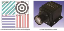
Polarization is the fourth important “information dimension” parameter in addition to intensity, wavelength and phase to describe the basic properties of electromagnetic waves. The polarization characteristics of reflected or radiated light are closely related to its material, geometry, structure and surface roughness, and physicochemical properties. Polarimetric optical imaging is a novel optical imaging method based on detecting the polarization information of light, which takes advantages of the difference in polarization characteristics between the reflected light and the background stray light to improve the target imaging quality, increase the action distance, enhance the detection capability and the identification probability. As an effective complementary means to the intensity, spectral and infrared imaging methods, polarimetric optical imaging has important applications for target detection in complex background environments with low signal-to-noise ratio, strong scattering and low illumination environments. Based on the authors' years of research work in polarimetric optical imaging and detection, this paper provides a more detailed introduction to the research status of polarimetric optical imaging including the related devices, technologies and applications. We present a comprehensive analysis and introduction of the polarimetric optical imaging technology and camera, the development and the application status at home and abroad. There are mainly two types of the polarimetric optical imaging regimes, which include the division-of time polarimetric optical imaging system and the simultaneous polarimetric optical imaging system, the later one can be further classified into the division-of-amplitude system, the division-of-aperture system, and the division-of-focal-plane system. The Stoke matrix representation of polarized light closely related to polarimetric imaging and the basic imaging principle are briefly introduced. Some research works conducted by our research team in polarimetric camera development and polarimetric optical imaging detection are summarized in detail, involving the design and key devices as well as technologies of the division-of-aperture polarimetric imaging system, the information processing technologies and algorithms and applications of polarization image. To be more specific, we introduce a novel division-of-aperture chromatic polarimetric camera with full-polarization-state simultaneous detection, i.e., including three linearly polarized states (0°,45°,and 90°) and one right circularly polarized state. We also introduce a division-of-aperture polarimetric lens with full-polarization-state simultaneous detection, which can be easily assembled to a commercial camera to change it into a polarimetric camera. We solve the image registration problem in division-of-aperture polarimetric camera by combining the phase-only correlation algorithm, the Speeded-up Robust Features (SURF) algorithm, and the Random Sample Consensus (RANSAC) algorithm. We propose a novel polarimetric optical imaging regime, namely the division-of-aperture simultaneous system based on the specifically designed color-polarizer filter, which is used for coding both the spectrum and the polarization. We report our research works on the polarimetric dehazing/descattering imaging for fog and/or underwater environments based on the optimization of the Angle of Polarization (AoP), and the low-pass filter denoising. We also introduce image enhancement algorithms for target imaging, detection and/or identification, where the visible and the near-infrared polarimetric images are fused, or the high-resolution polarized images are reconstructed from the low-resolution polarized images, together with obtaining the high-resolution Degree of Polarization (DoP) image and the high-resolution AoP image. We show the physical model of the polarization 3D reconstruction imaging, together with its basic theory, method and the 3D imaging experimental results. We show some thoughts, suggestions and/or problems on the current techniques and development directions that need to be solved in polarimetric optical imaging research, which include the enhancement of the polarization measurement precision, the optimization design of the polarimetric optical imaging system, the advantages development/extension of the computational optical imaging techniques based on polarimetric image processing and optimization, and the applications of polarimetric optical imaging and detection techniques, etc.
Aug. 25, 2022Vol. 51 Issue 8 0851505 (2022)
Xincun DOU, Guangfa WANG, and Zhuohua DAI
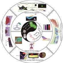
Explosives have resulted in numerous property losses, serious environmental pollution problems and even heavy casualties. Nowadays, military explosives have been mainly used by the national defense department. Owing to its great significance for sovereignty and territorial integrity, a huge effort has been devoted to developing various detection methods, such as surface-enhanced Raman spectroscope, ion mobility spectrometer, mass spectrometer. From these strategies, optical sensing explosive method stands out due to its ultralow detection limit, rapid response, facilitate portability as well as on-site visualization. However, with the increasingly strict peddling regulation, improvised explosives have been adopted as the ideal option of terrorists since their ingredients are readily available, low cost and legally purchased, as well as their destructive power is nearly equivalent to military explosives. This could be fully consolidated by the reported data from world media that more than 70% of the injuries and deaths in terrorist incidents are caused by improvised explosives. Resulted from approximate one hundred years of in-depth understanding of military explosives, optical sensing military explosives are relatively mature, while optical sensing improvised explosives are still in their infancy since the intrinsic properties of improvised explosives are completely different from that of military explosives such as they are non-volatile ionic crystal and extreme discrepancy of electronic configuration, which make the detection of improvised explosives extremely difficult and there is only limited reference significance to optical sensing improvised explosives. Therefore, developing an appropriate methodology for realizing optical sensing improvised explosives is urgent demand and central challenge for mitigating public security concerns via tracking beginnings, stemming their flow and qualitative identification of post-explosive residues.As the two main methods of optical sensing, colorimetric and fluorescent detection have attracted much attention and been attempted to detect improvised explosives in that their optical signal changes usually depend on specific chemical reactions. Taking full advantages of colorimetric and fluorescent detection, various probes have been orientedly designed including ligand modified inorganic materials, small moldcules, macromolecules and optical films. There are two main basic factors that determine the realization and properties of optical sensing, one is the specific binding affinity between probe and improvised explosives that directly determine the realization and specificity. The other one is maximum the optical signal change for enhancing sensitivity by regulating the chromophore or fluorophore according to the effect of specific binding affinity on the molecular vibration, molecular rotation and even electronic state. If the interferents in natural environment possess similar colorimetric or fluorescent signals, the detection results would be certain to cause fault. In recent decades, combining the complementary advantages of colorimetric detection and fluorescent detection, colorimetric/fluorescent dual-mode sensing strategy emerges and shows tremendous superiorities involving the elimination of fluorescent interferents by colorimetric signal and the elimination of colored interferents by fluorescent signal. Thus, the design strategy of colorimetric/fluorescent dual-mode probe will be systematically analyzed after summarizing the colorimetric or fluorescent methods toward improvised explosives.Along with the development of probe design, the ability of detecting improvised explosives has also progressed from ultralow concentration of solution, ultratrace solid residue to airborne improvised explosive microparticulate with the assistance of innovating substrates from solution, solid to hydrogel, which greatly facilitate the on-site detection of improvised explosives. However, there is still a tremendous lack of reviews from this viewpoint despite its great significance of practical applications. Thus, it is the right time to conclude the recent progress in colorimetric/fluorescent sensing toward improvised explosives, especially focusing on designing optical sensing materials with excellent specificity, developing a methodology of maximum change of optical signal and establishing a scientific paradigm of on-site sensing ultratrace improvised explosives. In this review, not only diverse methodologies have been summarized to provide a theoretical foundation of design optical sensing materials, but also the trend of developing novel strategy is systematically analyzed.
Aug. 25, 2022Vol. 51 Issue 8 0851507 (2022)
Yao ZHAO, Linhan LIN, and Hongbo SUN
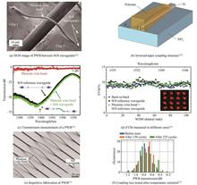
Integrated photonic chip is a combination of optoelectronic devices such as laser light sources, low-loss waveguides, modulators, detectors, etc., to achieving specific functionality. Integrated photonic chip provides important applications in high-speed optical communication, quantum information processing, optical sensing, optical manipulation, and so on. However, the fabrication of optoelectronic devices relies on different materials, it is extremely difficult to achieve photonic integration. The traditional heterogeneous integration and monolithic integration methods cannot simultaneously solve the problems such as low positioning accuracy, low scalability, high loss, and low bandwidth. Inspired by the direct wire bonding of three-dimensional electrodeposition of metals and conductive polymer, a Direct Optical Wire (DOW) technique has been recently proposed. This technology utilizes the rapid volatilization of solvents in extruded polymer liquids to create arched polymer pathways for conducting light between single-mode fiber and gratings. However, the cross-section and path are not completely controllable and the accuracy is low, limiting the implementation of small interface and low transmission loss. Femtosecond laser has extremely high pulse power, which triggers the two-photon absorption at the focal point and cause crosslinking of the photoresist material. The two-photon absorption efficiency is proportional to the square of the light intensity, and the absorbed light intensity will rapidly decay with the distance from the focal point, so the resolution of Two-Photon Polymerization (TPP) can break the diffraction limit, with the lateral resolution below 100 nm. In addition, two-photon polymerization enables true three-dimensional, mask-free, and custom machining with high degrees of freedom, becoming an indispensable tool in the field of micro-nano additive manufacturing. In this paper, we review the field of laser additive manufacturing of on-chip optical components for photonic chip integration including Photonic Wire Bonding (PWB) and micro-space optical devices, and summarizes the development status of existing technologies, and the perspective of future development.PWB uses femtosecond laser for direct writing of polymer waveguides, leading to direct optical interconnection between different optical interfaces. During on-chip interconnect, the interface of the optical device, such as the refractive index distribution, spatial position, size, and orientation, are different from each other. PWB technology is able to solve the mismatching of multi-material optoelectronic devices in size, mold field and spatial layout. It allows connection of optical devices with low alignment accuracy (at the order of 10 μm), reducing the need of active alignment. Researchers used femtosecond laser to write polymer waveguide inside the SU8 photoresist to achieve on-chip optical interconnection between two SOI waveguides. To enable efficient coupling at the interface, they designed an inverted cone structure, reducing the coupling loss down to 1.6 dB. PWB was also applied on Si3N4 devices and optical connection between SOI waveguide and multi-core fiber. It exhibits good repeatability and thermal stability. In order to eliminate edge delamination caused by layer-by-layer scanning, spiral machining was carried out inside the structure to crosslink the structure, and a smooth shell was then written to reduce loss.Efficient coupling of Ⅲ/Ⅴ group light sources to silicon photonic circuits is one of the key challenges of integrated optics. PWB can also solve this key problem. The coupling between an InP based Horizontal Cavity Surface Emitting Laser (HCSEL) and a silicon photonic platform has been achieved. Due to the error in the tilt angle of the HCSEL deflector, the laser emission direction and the surface of the chip are not strictly vertical. Thus, the initial orientation of the PWB structure has to be adjusted accordingly. At the same time, in order to achieve mold field matching between the two interfaces, the shape of PWB has to be customized. For example, by processing the coupling gradient structure, the collection and deflection of the HCSEL laser can be achieved. Combining InP laser, silicon photonic modulators and Si waveguide, an eight-channel transmitter exhibits very good performance, offering an aggregate line rate of 448 Gbit/s.Different from the PWB technology, the technical scheme of the micro-space optical device does not involve the direct physical connection between two ports. However, through optical fabrication of micro-space optical device, such as micro reflectors, micro couplers, micro prisms, etc., the input space light or guided light signal can be processed, and then output in the form of space light or guided light. Micro-space optical device can realize the free conduction and characteristic transformation of optical signals, which is an important part of integrated optics. The concept of on-chip micro-space optical elements by TPP has long been proposed. A couple of optical devices, such as three-dimensional photonic crystals and phase-type Fresnel waveband sheets have been fabricated, while the latter achieves a diffraction efficiency of up to 68%. The fabrication of multilayer couplers, artificial compound eyes, and on-chip polarization rotators have also been demonstrated.With high precision and strong penetration, femtosecond laser is used as a tool to fabricate various three-dimensional polymer structures. Unique optical components are designed according to the characteristics of the optical chip, which is unattainable using traditional lithography technology. The highly freedom of femtosecond lasers greatly improve the alignment accuracy and enables mask-free machining. In the future, laser additive manufacturing will be applied to fabricate more complex microstructures based on more materials. Technical developments such as accurate image recognition and positioning in complex environments, wide horizontal and longitudinal range of processing, and reconfigurable fabrication, are expected to extend its application in three-dimensional optical chips.
Aug. 25, 2022Vol. 51 Issue 8 0851512 (2022)
Xue CAO, Feng LI, Hualong ZHAO, Yishan WANG, Wei ZHOU, and Deyuan SHEN
Femtosecond laser with high repetition rate and high output power can be used as the driving light source of attosecond pulse generation, which can effectively increase photon flux, obtain enough experimental data quickly, and overcome the existing problem of space charge effect. Therefore, it has important application value in high order harmonics and attosecond pulse generation. At the same time, high repetition rate and high output power femtosecond pulses also have important application prospects in ultrafast laser precision micro-machining field, which can solve the technical problems of hard, brittle and soft materials processing with high-precision and high-quality “cold machining” in aviation and aerospace field. With the rapid development of ultra-fast laser processing market, high power femtosecond laser system with higher cost performance has become the major factor of concern in the industry.Compared with traditional solid-state lasers, fiber amplifiers have many characteristics, such as easy operation, all-fiber fusion, easy integration, excellent heat dissipation performance, excellent beam quality, etc., which have attracted much attention in the field of ultra-short pulse amplification. However, limited by the mode field area of ordinary single-mode or nearly single-mode fiber, the output energy of the ultrashort pulse based on the structure of optical fiber amplifier system is limited due to the Raman scattering and stimulated brillouin scattering, the self-phase modulation, cross phase modulation and other nonlinear effect in the process of high power pulse amplification. In order to achieve high energy femtosecond pulse amplification, the current fiber amplification system mainly adopts the structure of CPA system. Before amplification, the pulse is stretched in the time domain and the special fiber with large mode area is used to achieve high energy output in the space domain.Slab, disc and other solid amplifying media can output higher pulse energy,however,they are difficult to package, and the amplification structure is relatively complex, which is not conducive to the mass production of domestic lasers. Single crystal fiber as a new type of amplifier gain medium, it has a slender crystal structure and waveguide transmission characteristics for pump beam, which makes it have the advantages of both crystal and fiber laser amplification media. Its slender crystal structure can effectively dissipate heat, ensuring high beam quality under high-power operation. The waveguide characteristics of pump beam make it have greater energy extraction efficiency and higher amplification gain than traditional crystal rods. Compared with the fiber amplifier, the nonlinear accumulation of the single crystal fiber amplifier is much smaller, which is more conducive to the improvement of pulse energy. Meanwhile, the amplification structure of the single-crystal fiber amplifier mainly focuses on the single-pass or double-pass traveling wave amplification structure. Compared with the high complexity of the slab and thin-disk amplification system, the single-crystal fiber has better integration and stability. The waveguide structure of single-crystal fiber amplifier can match the multi-mode pump beam with the signal beam propagating in free space, which can obtain higher amplification efficiency and better beam quality than the traditional crystal rods. Excellent thermal management performance also enables the structure to achieve hundred-watt level ultra-short pulse output with good optical parameters. The hybrid fiber-single crystal fiber ultrashort pulse amplification system combined the high gain property of fiber laser and high peak power property of crystal gain medium. In order to further improve the average power and pulse energy, it has been less effective by simply stretching the pulse duration in time domain and increasing the optical fiber mode area in the space domain, technologies such as coherent beam combination can obtain much higher power and larger energy.When the output power of the laser is less than 200 W, the single crystal fiber can consitute a simple and reliable amplification setup. For higher power output, it can also be used as a stable, cost-effective seeder with good optical parameters for solid state amplifier, such as thin-disk lasers. In the future development of lasers, the research and development of fiber laser with appropriate wavelength for pump source and the continuous optimization of brightness of fiber coupled laser diode can effectively improve the amplification efficiency of ytterbium-doped single crystal fiber, and achieve a wider application in the field of ultrafast laser. The cladding structure of crystal fiber can increase the ratio of surface area to volume of single crystal fiber, by improving the heat transfer performance of cladding and the thermal management ability of fiber can realize the long distance fundamental mode waveguide, and finally realize the high power laser with higher efficiency, which is also an important direction of future development. Therefore, single crystal fiber as amplification gain medium has been widely used in ultrashort pulse amplification and has important application prospects in scientific research, national defense, industrial processing and other fields.This paper mainly introduces the structure and preparation methods of single crystal fiber, and the main research methods and results of ultrashort pulse amplification technology based on single crystal fiber in 1 μm waveband, including the main progress made by our research group, the prospect and development direction of single crystal fiber amplification technology are also discussed and prospected.
Aug. 25, 2022Vol. 51 Issue 8 0851513 (2022)

Zhishan GAO, Qun YUAN, Yifeng SUN, Jianqiu MA, Zhenyan GUO, Dan ZHU, Yuqing ZHAO, Xiao HUO, Shumin WANG, Jiale ZHANG, Xing ZHOU, Chunxia WU, and Xiaoxin FAN
The micro and nano scale microstructure can modulate the light field and increase the sensitivity of the sensor, is an important structure widely used in a new generation of functional devices or sensor devices. With the rapid development of advanced manufacturing technology including micromachining, laser direct writing and lithography, there is an urgent demand for nondestructive measurement technology of various types of micro and nano scale microstructure. In order to show much more knowledge about metrology of micro-structure as far as possible, this paper reviews the types of micro-structure in the development of industry in China and abroad. Focusing on the optical microscopy technology with the characteristics of high-precision nondestructive testing, this paper reviews four major methods of microstructure nondestructive testing that are still developing in China and abroad: dark-field microscopy with machine vision, confocal axial scanning microscopy, coherence spectral inversion combined with through-focus scanning optical microscopy, and low-coherence interferometric microscopy. This paper reviews the technical characteristics of these four methods, the test results of typical samples with these methods are individually given, some of which are published for the first time. These nondestructive testing methods are based on the diffraction-limited imaging principle of the optical microscope. The theoretical model of imaging can be unified, and the light intensity distribution function of the image field is given in this paper. The optical configurations of four major optical microscopes are all shown in the paper. The results show that the dark field microscopic imaging method is an effective method to detect harmful microstructures such as intensity-type particles, pits and scratches. Through the two-dimensional rapid scanning of the sample in the sample plane perpendicular to the optical axis, the rapid detection of large-scale samples can be realized, some measurement maps of large-scale fused silica flat and thin film transistor display screen are given in this paper; Confocal microscopic imaging and low coherence microscopic interferometry are the best detection methods of phase-type microstructure. They both need to make relative motion between the optical microscope and the sample to complete the vertical scanning, which can obtain the three-dimensional tomography of the microstructure sample. Three dimensional topography detection results of two-type gratings by confocal microscopy are provided and three dimensional topography of super-lens by white light low-coherence interferometric microscope is also given. We also review the theoretical reason of the bat effect on step type microstructure result. If the near-infrared light source is used with penetration ability to silicon-based materials instead of white light source, and in the meantime, the active compensator is used to compensate for the modulation aberration of detection beam induced by microstructure, the silicon-based microstructure with a high aspect ratio can be detected. By the way, some maps of three-dimensional tomography of MEMs microstructure on Si-substrate are given. The combination method of coherence spectral inversion and through-focus scanning optical microscopy is also effective on the measurement of high aspect ratio microstructure. The coherence spectral inversion method is used to obtain the height of the microstructure with a low numerical aperture microscope. In the meantime, the through-focus scanning method is used to obtain the critical dimension with a large numerical aperture microscope. Coherence spectral inversion combined with through-focus scanning optical microscopy and near-infrared interferometric microscopy is new methods developed to meet the needs of nondestructive testing of high aspect ratio microstructure. The former can quickly measure the linewidth and depth, and the latter can measure the three-dimensional tomography of high aspect ratio microstructure in the field of view of the objective lens. They can verify and supplement each other. In this paper, we describe the advantage and disadvantage of the above four major methods of microstructure nondestructive testing in detail from the multi angle of view, and discuss the new variability from the four major methods.
Aug. 25, 2022Vol. 51 Issue 8 0851501 (2022)
Shuxia QI, Sheng LIU, Peng LI, Bingyan WEI, Mengmeng ZHANG, Jiazhen DOU, Jiwei ZHAGN, and Jianlin ZHAO
Polarization, as one of the important properties of light, plays a very important role in the light field research and practical applications. The polarization measurement of the light field, especially the polarization distribution measurement of the light field with complex spatial structure, is an important subject to study the polarization characteristics of the light field and its application. Recently, as one of the main contents of the light field manipulation, the spatial modulation on the polarization state of light has become a hot topic. The spatial modulation for polarization of the light field constitutes a new class of laser beams with the characteristics of spatially varied polarization, also named vector beams. Owing to the unique properties of the spatially variant polarization and tight focusing, vector beams have received extensive attention in many scientific and engineering applications, such as femtosecond laser processing, super-resolution microscopy, optical micro-manipulation, and optical communication. Besides, the spatial modulation of polarization of the light field also enables spin-orbit interaction and polarization-related dynamic transmission behaviors, such as analogous optical activity in free space, polarization controlled Airy beam, spin selective imaging, etc. The propagation dynamics of the light field mainly depend on its polarization and phase distribution. Therefore, how to accurately and rapidly measure the polarization and phase distribution of the light field is a key problem in exploring new optical effects and enrich the related applications. On the other hand, as a carrier of light information, polarization plays an important role in the interaction between light and matter. By detecting the polarization information of the light field passing through the medium, the information about the composition and structure of the interacting materials can be obtained. Especially for the anisotropic materials, the polarization response can reveal the intrinsic structure and composition of materials, as well as the essential properties of scattering, emission and absorption. Therefore, measuring the polarization response of materials is of great significance for revealing the internal structure and birefringence property of materials, characterizing the complex modulation properties of optical devices, and exploring the physical mechanism of light-matter interaction. This review presents an overview of the recent advances of polarization measurement methods for the light field and optical anisotropy of materials. Firstly, the four representations of the polarization state of the light field are introduced, including polarization ellipse, Jones vector, Stokes parameters, and Poincaré sphere. Then, the measurement methods of Stokes parameters describing the polarization of the light fields and the Jones matrix of the anisotropic material are introduced, respectively. One of the measurement schemes for the Stokes parameters of the light fields is to record the intensity distributions at different detection states, where the most common one is the combination of a rotating retarder and a fixed analyzer. Due to time-sequential operation of rotating optical elements in the measurement process, it is unfavorable for fast measurement. The measurement speed can be improved by the multichannel simultaneous measurement. In this case, the amplitude of light field is divided into several channels, each of which is analyzed by suitable polarization optical elements. However, the measurement systems are complicated and cumbersome. With the development of micro-nano processing technology, the polarization measurement based on the metasurface can integrate the traditional polarization measurement system into a compact element, which can be further combined with a lens and image sensor to form full-Stokes polarization cameras. Another scheme for measuring Stokes parameters is based on the Pancharatnam-Berry (PB) phase theory and digital holography. It can not only greatly improve the measurement speed, but also obtain complete information of light fields, including the amplitude, phase, and polarization distributions in three-dimensional space. For the Jones matrix measurement of anisotropic materials, several measurement methods and their related applications based on digital holography are mainly introduced. From another point of view, the traditional intensity methods of polarization measurement are restricted to some specific application scenarios. These limits can be exceeded by introducing the well-designed metasurface elements, which cannot still measure the phase distribution. The polarization measurement method based on digital holography has the advantage of obtaining complete information of the light field, but it requires an interference optical path to provide a reference light beam. Therefore, we can choose different polarization measurement methods according to the practical application. Finally, for the Stokes parameters of light fields or the Jones matrix of materials, the development trend of polarization measurement technology is integration and rapidity.
Aug. 25, 2022Vol. 51 Issue 8 0851502 (2022)
Tao ZHU, Laiyang DANG, Jiali LI, Tianyi LAN, Ligang HUANG, and Leilei SHI
Narrow linewidth lasers have extremely high spectral purity, high peak spectral density, ultra-long coherence length and extremely low phase noise, so they are used as core light sources in fields of gravitational wave detection, optical clocks, cold atom physics, coherent optical communication, optical precision measurement and microwave photonic signal processing. With the development of laser and its application research, higher and higher requirements are placed on the comprehensive parameter performance of lasers. Narrow linewidth lasers are developing in the direction of ultra-narrow linewidth, ultra-stable time-frequency parameter and wavelength arbitrary tunability. Among them, the laser linewidth is the key factor that determines laser coherence, and it has always been the focus of scientists' research on laser technology. The essence of the existence of linewidth is that the laser will be affected by the phase and intensity disturbances caused by spontaneous radiation in the gain during operation, which makes the laser output signal inherently broadened by Gaussian white noise. In addition, the laser is also easily affected by the classical noise caused by the temperature change and vibration in the external environment, which further widens the laser linewidth. The above-mentioned factors have greatly reduced the coherence of the laser, thus limiting the development of the laser in promoting scientific research and industrial application to a great extent. Therefore, laser linewidth compression technology has become a key scientific issue for obtaining high-coherence light sources. At present, lasers with fiber-doped rare earth ions and semiconductors as gain have the advantages of long life, small size, low cost, high reliability, and easy industrialization, and have become the most studied and widely used solid-state lasers. However, due to the lack of control technology, the linewidth of conventional short-cavity fiber and semiconductor lasers is usually maintained at the order of tens of kHz or even MHz, and it is difficult to meet the requirements of various technological developments for the performance of laser linewidth parameters. Based on the interaction principle of the spontaneous emission and stimulated emission in the laser cavity, the structure innovation of the laser cavity is the main research routine to achieve the extreme control of narrow linewidth laser parameters. Since the invention of the laser, it has gradually experienced three stages of cavity structures to suppress the spontaneous emission: the main cavity laser, the fixed external-cavity feedback laser, and the adaptive distributed feedback laser. Here, the laser frequency stabilization technology based on the external servo electrical feedback and the external cavity feedback technology based on the photon lifetime extension are the common means to realize the narrow linewidth laser output. However, the extra-cavity servo electrical feedback technology not only requires high-precision and high-sensitivity external detection and control devices, but also requires precise control of the operating environment of the reference cavity. Hence, this laser frequency stabilization technology has a complex structure and high cost, which is not conducive to the large-scale integrated development of lasers. The latest laser structure with adaptive distributed feedback is mainly based on the fixed spatiotemporal perturbation provided by the distributed feedback, which deeply suppresses the random spatiotemporal perturbation by the spontaneous emission, so as to achieve the laser linewidth deep compression of the laser cavity with the feature of wavelength self-adaptation. This review first introduces the application requirements and structure evolution of narrow linewidth lasers, and then introduces the research progress of the main cavity laser and the fixed external-cavity feedback laser. Then, the adaptive distributed feedback laser recently developed is introduced. The physical ideas, core devices and system performance of this new type of laser are discussed. Eventually, the application characteristics of narrow linewidth lasers are introduced in typical fields of the distributed optical fiber sensing, laser coherent communication and on-chip optical information processing. The development trends of narrow linewidth lasers are also prospected.
Aug. 25, 2022Vol. 51 Issue 8 0851503 (2022)
Baojiu CHEN, Xin CHEN, Li WANG, Yizhuo WANG, Lei LI, and Sai XU
At the end of this review, the present status of the luminescence anti-counterfeiting materials was concluded. The problems and obstacles to developing luminescence anti-counterfeiting labels were summarized. Some ideas for future progress were also proposed. It was figured out that the emission wavelengths for the present luminescence anti-counterfeiting materials are mainly in the visible region, thus resulting in easy counterfeiting and cloning. Therefore, developing novel luminescence anti-counterfeiting materials with emitting wavelengths other than visible wavelengths may be a good proposal. In many articles, more than one stimuli source were used, thus in fact is not a good way since the multi-excitation sources would result in complicated identification and high cost. Therefore, developing chemical-assisted luminescence anti-counterfeiting materials is more significant and meaningful. It should also be pointed out that the luminescence anti-counterfeiting materials with similar spectral properties to the commercialized phosphors are useless and dangerous since the counterfeiting and cloning behaviors are easy by using the commercialized phosphors in this sense. Finally, the combination of online and offline identifications is suggested while the 5G technique is widely used.
Aug. 25, 2022Vol. 51 Issue 8 0851504 (2022)
Peng GAO, Xiang FANG, Kai WEN, Yunze LEI, Zihan XIONG, Jiaoyue LI, Xing LIU, Juanjuan ZHENG, and Sha AN
The proposed method also has disadvantages: first, the period of the fringe/lattice patterns can not be varied digitally like what in SLM/DMD-based SIM. Second, the resolution enhancement achieved with this method is less isotropic than the standard 3-angle 2-beam SIM. Both drawbacks can be solved by using a specially-designed Diffractive Optical Element (DOE) instead of the 2D grating used in the current technique and by recording more raw images under different phase-shift combinations. Once using a 2D amplitude grating that has the same transmittance for different illumination wavelengths, the large-field SIM also allows multi-color SIM imaging. We can envisage that the proposed method can be applied to many fields, including biomedical, industrial, and chemical fields.
Aug. 25, 2022Vol. 51 Issue 8 0851506 (2022)
Xueli CHEN, Xinyu WANG, Tianyu YAN, Qi ZENG, Xinyi XU, and Hui XIE
This paper firstly outlines the concept and characteristics of Bessel beams, as well as the commonly used laboratory generation methods, including the generation using a ring slit, using an axicon, and using a spatial light modulator, etc. The authors then summarize the applications of the Bessel beams in biomedical optical microscopy techniques in recent years, focusing on their applications in the fields of multiphoton fluorescence microscopy, light-sheet fluorescence microimaging, Raman microimaging, and other techniques. The authors summarize the advantages of Bessel beams, including extended depth-of-field imaging based on diffraction-free properties, large-depth imaging based on self-reconfiguration properties, and high-resolution imaging based on finer-focused beams, and also analyze the solutions to eliminate the interference problems caused by side rings of the Bessel beam. In addition, the authors also briefly describe the exploration and application of Bessel beams in other imaging modalities, including the technical areas of optical coherent tomography, optical coherent elastography, photoacoustic imaging, second harmonic imaging, third harmonic imaging, and Fourier multiplexed fluorescence lifetime tomographic imaging. The article concludes with an analysis and discussion of the problems encountered in the application of Bessel beams in biomedical optical microscopy and the prospects for development.
Aug. 25, 2022Vol. 51 Issue 8 0851508 (2022)
Lin LI, Duoteng ZHANG, and Yunwei QU
Finally, we look forward to the development direction of small molecule dyes and propose for novel super-resolution fluorescent dyes/probes to achieve high membrane permeability, excellent precision positioning ability, high brightness and stability, and low phototoxicity of dye molecules without increasing the size of dye molecules as much as possible. This paper summarized the structural design characteristics of organic small molecule dyes selected for different techniques with respect to the requirements of different super-resolution imaging techniques for dye performance. It provides ideas for the development of new dyes suitable for super-resolution imaging.
Aug. 25, 2022Vol. 51 Issue 8 0851509 (2022)
Mingjie SUN, and Zhiguan WANG
Single-photon avalanche diodes are widely used in various fields because of their single-photon sensitivity and excellent time-resolved performance. With the development of semiconductor technology, single-photon avalanche diode arrays integrating multiple pixels and time measurement circuits are gradually popularized, with the ability to collect photon information in parallel. Imaging is a means of obtaining information of the target object through photons, and imaging systems based on single-photon avalanche diodes can use richer photon counts and temporal information to detect the target in extreme environments. Single-photon avalanche diode arrays have higher detection efficiency, which can replace the detection system of single-pixel detectors and scanning structures, promoting the advancement of biological microscopy, scattering imaging and lidar technologies. This manuscript concludes the development of single-photon avalanche diode arrays and introduces some typical applications of single-photon avalanche diode arrays in imaging. The development of SPAD is similar to other photodetectors, which have gone through the process from single-point detectors to multi-pixel arrays. Because of the application of CMOS technology, SPAD arrays have developed rapidly in terms of pixel scale and circuit integration. Megapixel SPAD arrays with time measurement capabilities are available nowadays. While the pixel scale is gradually increasing, important parameters such as photon detection efficiency, dark count rate, spectral response range, and temporal resolution are also continuously optimized with the development of related technologies. Optical imaging has a long history. With the development of science and technology, people's research interests have gradually expanded from traditional imaging to imaging under extreme conditions, such as super-resolution imaging, extremely low-light imaging, and over-the-horizon imaging. SPAD has single-photon sensitivity and ps-level temporal resolution, which enables obtaining photon information under extreme conditions. As the performance of early SPAD arrays were not perfect, single-pixel SPAD detectors are often combined with a scanning device to obtain two-dimensional images. With the development of SPAD arrays, in applications that require real-time imaging, such as vehicle-based lidar, SPAD arrays have gradually replaced the scanning imaging systems because of their efficient parallel single-photon detection capabilities, providing higher imaging speed. Besides, many biophotonics applications have been explored with SPAD arrays, such as SMLM and FLIM. The use of SPAD arrays in these applications enables higher SNR, higher imaging speed, providing powerful method to investigate the structural details and molecular dynamics of cells. In addition, the high dynamic range images are accessible through a SPAD array, which has the potential to be applied in autonomous driving and object recognition. In scattering imaging and non-line-of-sight imaging, the emergence of SPAD arrays enables the complex photon propagation process caused by multipath, scattering or other factors to be distinguished in time domain and space domain, and the photon information can be combined with physical model or neural network to detect the target object which is outside the field of view or behind the scattering medium. Using the high temporal resolution and parallel acquisition capability of SPAD arrays, one can also track the high-speed laser pulses, providing more details of ultrafast optical phenomena. The low price and high integration of SPAD arrays are unmatched by other devices. In the future, if the cost of megapixel SPAD arrays can be reduced to a reasonable range, they will be widely used in scientific research, industry and military fields. However, the reported megapixel SPAD array is still in the laboratory verification stage, and there is still a long distance from the industrialization and commercialization. In addition, with the continuous increase of the pixel scale of SPAD arrays, the storage, processing and transmission of photonic data will be a difficult problem. Using high-performance FPGA to locally preprocess the photonic data can effectively reduce the demand for data storage, reducing the data transfer bandwidth between SPAD arrays and computers. In terms of spectral response, the spectral response peaks of silicon-based SPAD arrays are mainly within the visible light band. The photon detection probability of silicon-based SPAD arrays in the near-infrared band can be improved through structure and process optimization, enabling utilizing the strong penetration of near-infrared light to improve the detection range of lidar and scattering imaging. SPAD arrays based on InGaAs or InP can respond to short-wave infrared light above 1450 nm, so such SPAD arrays have great application potential in imaging with optical fibers and quantum optics. SPAD arrays can efficiently acquire spatiotemporal information of photons, and how to make full use of these photonic data is also a problem that needs to be solved in the application of SPAD arrays. In addition to establishing the physical model of photon propagation, data-driven algorithms such as deep learning can also be used to establish a correspondence between the spatiotemporal distribution of photon and target features from a higher dimension, enabling efficiently reveal the hidden information in the photonic data. In the future, SPAD arrays will play a more important role in optical imaging, providing more powerful tools to perceive and understand the world.
Aug. 25, 2022Vol. 51 Issue 8 0851510 (2022)
Yin SONG, Ruidan ZHU, Shuang YU, Xiaojuan CHUAI, Lirong QIU, and Weiqian ZHAO
Ultrafast Two-Dimensional Electronic Spectroscopy (2DES) has emerged as a powerful tool to probe excited-state dynamics in photosynthesis, photovoltaic materials, quantum dots, and two-dimensional materials in recent years. Compared to one-dimensional time-resolved spectroscopy, 2DES not only contains one additional dimension to resolve excited-state dynamics but also provides rich information about homogeneous and inhomogeneous broadening, intermolecular coupling and coherent dynamics that are not fully accessible to the traditional third-order spectroscopic methods. Here we will briefly introduce the principle of 2DES from the basic concepts such as Fourier-transform linear spectroscopy, and transient grating. Subsequently, we will illustrate the applications of 2DES in the context of recent studies of spectral broadening in two-dimensional materials, and charge separation and coherent dynamics in photosynthesis and photovoltaic materials. Finally, we will discuss the remaining challenges and exciting future directions for the fields of 2DES.
Aug. 25, 2022Vol. 51 Issue 8 0851511 (2022)
Dongyu LI, Tingting YU, Jingtan ZHU, and Dan ZHU
In summary, the novel in vivo skull optical clearing technique provides an optical window for cortical observation without craniotomy. Over the past decades, with the development of technique, there are a variety of skull optical clearing windows available, each with its own characteristics. Through the skull optical clearing window, various modern optical imaging techniques have been used to noninvasively monitor neurovascular information. Up to now, the skull optical clearing window holds the advantages of high resolution, large scale, long-term observation, and is compatible with immediate observation, therefore has great potential in the research of brain science and related diseases.
Aug. 25, 2022Vol. 51 Issue 8 0851514 (2022)
Tong WU, Chen QIAN, Zishao WANG, Xiangyu ZHANG, Chao YU, and Ruifeng LU
Light-matter interactions can be mainly described by transitions of electrons, accompanied by emission, absorption, or scattering of photons. Light absorption and emission of atoms, molecules, solids and other substances play a vital role in the development of science and technology.Because of its excellent monochromaticity, directivity and coherence, laser has become a powerful tool to detect the structure and properties of matter.With the development of laser technology, the peak power of the laser pulse reaches the order of 1015 W and the laser pulse durations decrease to a few femtoseconds. Advanced optical technology makes it possible to carry out experiments at an unprecedented intensity. When the electric field intensity of laser pulse reaches or even exceeds the electric field intensity of the Coulomb potential inside the substances, the concept that the laser field is regarded as a perturbation to the motion of electrons under the constraints of the Coulomb field is no longer applicable, accompanied by a series of highly nonlinear complex dynamic processes, such as multi-photon and above threshold ionization, tunneling ionization,nonsequential double ionization and High Harmonic Generation (HHG). In this context, the emergence of ultrashort and ultra-intense pulses gradually opened up the research of strong field physics. When a macroscopic system is exposed to intense laser fields whose forces are comparable to the binding forces of valence electrons, the system will emit coherent radiation with frequencies many times that of the driving laser field. This non-perturbativeand extremely nonlinear optical phenomenon is calledhigh-order harmonic generation, whichhas become a research direction of great concern in the field of strong field physicsas a Potential Extreme Ultraviolet (EUV) source and a possible means of real-time detection of ultrafast dynamics inside matter. In the past 30 years, HHG from gases has been developed greatly based on the physical image of the three-step model, which has laid a solid foundation for attosecond physics. HHG from solids provides a new way to miniaturize devices as a EUV light source and explore the electronic structure of condensed matter system. Meanwhile, in order to find more integrated and compact EUV light source, people gradually turn their attention to solid target.Experimental observation of non-perturbative transmitted high-order harmonics generated from ZnO crystal suggested that the solid-state HHG process can be illustrated neither by conventional perturbative nonlinear optics nor by the kinematics of strong-field re-scattering.More researches demonstrated that solid-state HHG can be achieved through a wide variety of interaction media with suitable laser wavelengths from the near-infrared to terahertz range.High harmonic generation from solid materials driven by an ultrafast strong laser is a fast developing direction in interdisciplinary fields of condensed matter physics, materials science, optics and photonics. So far, the target of solid-state HHG study has been expanded from bulk metals, semiconductors, insulators to low-dimensional nanostructures. Moreover, nonperturbative harmonic signals have been successfully detected in topological insulators and from topological surface states. Compared to gaseous atoms and molecules, solid materials have higher atomic density, and the mechanism of solid-state HHG is more complicated, thus solid-state HHG possesses good application prospects in achieving new light sources, exploring physical properties as well as characterizing microscopic dynamics of materials. This article mainly reviews the experimental and theoretical progresses of solid-state HHG in recent years, and also summarizes its mechanisms and potential applications.
Aug. 25, 2022Vol. 51 Issue 8 0851515 (2022)
Yang XIAO, Yutao FENG, Zhenqing WEN, and Di FU
Atmospheric wind field is an important parameter to understand the dynamics and thermodynamic characteristics of the Earth's atmospheric system, and it is the basic data for weather forecasting, space environment monitoring, and climatology research. Passive optical remote sensing based on Optical interferometer is the main technical means of wind field measurement in the middle and upper atmosphere. In the 1960s, foreign research institutions began to use optical interferometers to detect upper atmospheric wind fields. and carried out the experimental research on interferometer payload technology simultaneously, and successively developed a series of representative scientific instruments and satellite payloads based on the Fabry-Pérot interferometer and the Wide Angle Michelson interferometer. In 2006, the ENGLERT C R research team of the U.S. Naval Research Laboratory proposed a new planetary atmospheric wind detection technology, called Doppler Asymmetric Spatial Heterodyne wind measurement technology, this technology detects the Doppler frequency shift of the atmospheric airglow spectrum by inverting the phase of the interferogram, thereby realizing the detection of the atmospheric wind field. Compared with the Fabry-Perot interferometer and the Wide-Angle Michelson interferometer, the Doppler Asymmetric Spatial Heterodyne interferometer has the following advantages: 1)Two-beam equivalent thickness spatial modulation interference, which relaxes the requirements for the optical index of the element; 2) Interferometer does not need Step-by-step scanning; 3) Wind speed inversion is based on the Fourier transform relationship between interferogram and spectrogram, so it does not need extremely narrow bandwidth (<1 nm) filters to separate single-line spectra; 4)Synchronous calibration can be achieved, the standard spectral line of the calibration light source and the target spectral line of the detection source are simultaneously introduced into the interferometer system to monitor the state change of the interferometer in real time, therefore, the measurement accuracy can be further improved. After nearly two decades, a series of research results have been achieved in basic theory, interferometer design, instrument development technology, data processing and wind speed retrieval of Doppler Asymmetric Spatial Heterodyne Interferometer. In terms of theoretical research progress, domestic and foreign scholars have theoretically analyzed the factors that affect the accuracy of interferometer phase inversion; In order to expand the detection capability of the Doppler Asymmetric Spatial Heterodyne Interferometer, four structural design schemes are proposed by referring to the spectral expansion method of the wide-spectru Spatial Heterodyne Spectroscopy; A series of interferogram preprocessing methods are proposed to eliminate the errors of the original interferogram caused by various defects of optical components, photoelectric sensors and optical systems. Foreign scholars put forward a wind field profile inversion method named “peeling onions”. In terms of instrument research progress, since the Doppler Asymmetric Spatial Heterodyne Interferometer wind measurement technology was proposed in 2006, many international research institutions have carried out research on the development process of the core components of the interferometer, and successfully developed a variety of interferometer prototypes covering from visible light to long-wave infrared ,such as Michelson Interferometer for Global High-resolution Thermospheric Imaging (MIGHTI), Stratospheric Wind Interferometer for Transport studies- Doppler Asymmetric Spatial Heterodyne (SWIFT-DASH), and Redline DASH Demonstration Instrument (REDDI). Ground-based instruments and space-based payloads have also been developed to the stage of application and promotion. The main domestic research institute is the Xi'an Institute of Optics and Precision Mechanics of CAS, the institute focuses on the study of the interferometer thermal compensation method, the interferometer glass component design method, the interferometer component gluing and integration process, the interferometer support structure component design and integration process, and proposed a dual-band Doppler Asymmetric Spatial Heterodyne interferometer technology and a high-time-resolution ground-based Doppler Asymmetric Spatial Heterodyne interferometer technology, and developed a single-channel DASH principle prototype with oxygen atom 630 nm and oxygen molecule 867 nm airglow radiation as the target source.This paper reviews the domestic and foreign research progress of Doppler Asymmetric Spatial Heterodyne technology for atmospheric wind field detection, discusses its technical characteristics and application potential, and provides reference for the future development of atmospheric wind field passive optical remote sensing detection technology and mission planning in the field of atmospheric wind field detection in our country.
Aug. 25, 2022Vol. 51 Issue 8 0851516 (2022)
Yuehan ZHAO, and Xiang HAO
Finally, we present an outlook on the fast-growing field of multicolor single-molecule localization microscopy. One of the future development directions of multicolor single molecules is the research on probes, including the brighter organic fluorescent dyes or fluorescent proteins and more universal imaging buffers. Further research can also be done on reducing the complexity of the optical system and expanding the field of view of imaging. It can be envisioned that multicolor SMLM will play a more prominent role in biological and medical research for many years to come. We hope that this review can help researchers choose the appropriate multicolor SMLM for their own experiments.
Aug. 25, 2022Vol. 51 Issue 8 0851517 (2022)
Jiajun PENG, Xiaohui LI, Sunfan XI, and Keqin JIAO
The convergence of machine learning and ultrafast photonics cutting-edge crossover technologies in the context of artificial intelligence takes an unconventional approach to provide an unparalleled photonic perspective. This intersection of computer science, photonics, and materials platforms will enable new approaches to the large-scale photonic design of unique functions as well as optical characterization, laying the cornerstone for efficient energy conversion systems. We envision that a global optimization framework based on a multi-step machine learning strategy can build a more general intelligent ultrafast photonic system, where the first step can be to define the main target function of the device and determine the appropriate photonic concept to provide the best performance. The second step is to select a suitable material platform and build an extensive database of optical materials. By using the selected material properties, an optimized design solution for the material device can be provided. The third step is to determine the appropriate fabrication conditions (growth conditions, doping levels, stoichiometry, etc.) and integration schemes. The interplay between new photonic structures and machine learning may overcome the limitations of current computational methods and systems, provide unparalleled capabilities in light-matter interactions and unlock new device concepts, and may lead ultrafast photonics research to new frontiers that could usher in a brighter era of artificial intelligence.
Aug. 25, 2022Vol. 51 Issue 8 0851518 (2022)
Shiwei LIU, Difa YE, and Jie LIU
The interaction between atoms and intense laser fields plays an important role in the field of ultrafast physics, which has become a powerful experimental technique to explore the structure and dynamics of matter. One of the critical issues is to explore the mechanism of laser-driven electron re-scattering process in, e.g., above-threshold ionization, high-order harmonic generation, and Non-Sequential Double/Multiple Ionization (NSDI/NSMI). Among them, the NSDI/NSMI is particularly interesting since it is a prototypical example for studying the electron-electron (e-e) correlation. During the past years, the general picture of NSDI has been established. In comparison, the NSMI is less well-understood although a series of experimental data have been collected, for example, extremely highly charged ions up to Ar16+, Kr19+, and Xe26+ have been produced in super-strong laser fields. Here, the involvement of the multi-shell multi-electron, as well as highly nonlinear relativistic and non-dipole effects, makes the electron dynamics much more complicated. As a result, the theoretical explanation is hindered and lagged far behind partially due to the fact that solving the full-dimensional Time-Dependent Schrödinger Equation (TDSE) is currently limited to two-electron systems, leaving the dynamics of NSMI highly unexplored. On the other aspect, the Classical Trajectory Monte Carlo (CTMC) approach has been widely applied to atomic and molecular collisions and ionization of atoms by strong laser fields, which can be readily implemented in many-body systems and provide intuitive pictures to the dynamical processes of interest. It should be noted that, however, a classical multi-electron atom with Coulomb interactions is typically unstable and might suffer nonphysical auto-ionization, which needs feasible 'quantum' modifications. this article investigates the laser-driven lithium triple ionization by the classical trajectory Monte Carlo with the Heisenberg potential (CTMC-H) model. The model introduces the Heisenberg potential to mimic the Heisenberg uncertainty principle, which can be applied to obtain the classical stable configuration of the ground state of lithium atom by minimizing the system Hamiltonian to the values of the ionization energies. By solving the classical canonical equations of electrons, we study the total ionization rate of Li in a wide range of laser intensities. Due to the unique shell structure of the alkali metal elements, the out-most electron of the lithium atom is loosely bound and can be easily ionized, while the inner shell electrons are deeply bound and difficult to be deprived because of the much larger ionization energy. Therefore, we find that the single ionization is saturated over a wide span of laser intensities, and the double and triple ionization can be triggered by the re-collision of the out-most electron, showing the typical knee structure around 30 and 60 PW/cm2, respectively. The difference between sequential triple ionization and non-sequential triple ionization is described in detail by plotting the momentum distribution of Li3+ in the polarization direction of the laser electric field, which shows a single peak structure near zero for the STI process and a double-hump structure in the NSTI regime as another signature of re-collision. Meanwhile, the magnetic effect is revealed by comparing the momentum spectra of Li3+ along the magnetic field polarization direction and the laser beam propagation direction. According to the energy distribution of three electrons mapped into the Dalitz diagram, we identify three types of re-collision mechanisms for the non-sequential triple ionization and reveal the fingerprint of thermalization induced by the (e, 3e) scattering mechanism. Besides, the electron re-scattering process is significant even in the sequential triple ionization region, e.g., at 100 PW/cm2, as evidenced by the high-energy electrons located at the corners of the Dalitz plot. These findings not only provide deep insight into the mechanisms of the multiple ionization of alkali metal atoms in a femtosecond strong laser field but also have potential applications in manipulating the electron correlation on the attosecond time scale. Finally, we would like to emphasize that recently the magneto-optical trap recoil ion momentum spectroscopy has been proposed and established by combining cold atom trapping technology, strong laser pulse, and ultra-fast technology, exhibiting the ability to measure the full-dimensional momentum spectra of multiple reaction products and thus extending the study of strong-field multiple ionization and ultra-fast processes to the alkali metal atoms. We hope our theoretical predictions might stimulate experiments in this direction.
Aug. 25, 2022Vol. 51 Issue 8 0851519 (2022)
© Copyright 2018-2021 | Chinese Laser Press.
All Rights Reserved 沪ICP备15018463号-20