


Please enter the answer below before you can view the full text.

2021
Volume: 41 Issue 8
21 Article(s)

Kun Liao, Tianyi Gan, Xiaoyong Hu, and Qihuang Gong
Metasurfaces can be designed for the spatial transformation of wavefronts. Research on the two-dimensional periodic optical metasurfaces mainly focuses on controlling the wavefront of light propagating in free space. In recent years, researchers have designed a series of one-dimensional on-chip metasurfaces to control the degree of freedom in on-chip optical signal transmission and further realize a small-size, broadband, and low-loss integrated photonic computing chip. This article summarized the related work on on-chip nanophotonic devices based on dielectric metasurfaces. To be specific, we reviewed and discussed the physical mechanisms, implementation methods, and applications of on-chip metasurfaces in integrated nanophotonic devices. Besides, we undertook a general review of the remaining challenges and proposed possible development directions that require further study for the application of on-chip metasurfaces to integrated nanophotonic devices.
Apr. 09, 2021Vol. 41 Issue 8 0823001 (2021)
Runqiu He, Guohua Liang, Hui Liu, and Shining Zhu
Metamaterial, as a groundbreaking artificial material, plays a revolutionary role in the field of electromagnetic wave control. A combination of transformation optics with metamaterials can not only give full play to the wonderful properties of metamaterials and realize many magical effects but also be applied to optical simulation, displaying some cosmological phenomena that cannot be observed directly. However, due to the limitation of the metamaterial structure, some electromagnetic parameters cannot be controlled by the microstructure, and then curved surfaces start to attract attention of people. It has been found that waveguides with curved structures can also regulate electromagnetic waves and break through some limitations of metamaterials to achieve many novel effects. By introducing a series of work on curved waveguides by research group of Liu Hui in Nanjing University, the wonderful applications of curved waveguides in various directions are demonstrated, and the application prospects of curved waveguides are discussed.
Apr. 09, 2021Vol. 41 Issue 8 0823002 (2021)
Xiaoze Liu, Xinyuan Zhang, Shunping Zhang, Zhiqiang Guan, and Hongxing Xu
Two dimensional (2D) semiconductors have unique 2D material properties, novel valley electron energy band structure, and abundant regulatory degree of freedom, which bring opportunities for the research of condensed matter physics, optics, and other fields. However, these studies still have many fundamental problems, such as low efficiency of light utilization and susceptibility to environmental disturbance of quantum properties. The coupling of two-dimensional semiconductors and precision micro-nano optical cavities not only provides a suitable solution for these problems, but also exhibits unprecedented and novel optical effects, thus opening up new research directions for the basic physical research and optoelectronic applications of 2D semiconductors. The research progress of light-material coupling of 2D semiconductors in micro-nano optical cavities in the past 10 years is reviewed. This paper also focuses on the optical properties of 2D semiconductors, the research progress and control mechanism of different coupling regions between the 2D semiconductor and micro-nano optical cavity, and its potential applications in nano laser source, valley electronics, quantum optics, etc. The future development direction and opportunities are also prospected.
Apr. 09, 2021Vol. 41 Issue 8 0823003 (2021)
Che Liu, Qian Ma, Lianlin Li, and Tiejun Cui
The development of artificial intelligence (AI) has brought great revolutions to the development of human society, and new applications based on AI have been continuously emerging. Owing to the powerful capability in controlling electromagnetic (EM) waves and the flexible designs of EM and optical metamaterials, especially the real-time digital control abilities of programmable metamaterials, the AI technologies could easily be brought into the design and intelligent applications of EM metamaterials. As for the AI technology combined with electromagnetic and optical metamaterials, this paper reviews the main research progresses and achievements of structural optimization, architectural design, and system applications from the three aspects of intelligent design, neuromorphic architecture, and smart system. In addition, the future development direction of intelligent metamaterials is prospected.
Apr. 09, 2021Vol. 41 Issue 8 0823004 (2021)
Haitao Luan, Xi Chen, Qiming Zhang, Haoyi Yu, and Min Gu
Innovations in artificial intelligence, particularly artificial neural networks, have revolutionized applications in many areas, such as big-data search, computer recognition, and language and image recognition. The development of nanophotonics in the past decades has brought physical perspectives and different approaches to the implementation and the development of traditional artificial neural network technologies, especially optical neural networks. On the one hand, nanophotonics is a field studying the interaction of light and matter at the nanoscale, which can lead to new techniques, such as super-resolution optical lithography and super-resolution optical imaging technology, therefore in turn promoting the implementation of optical neural networks with multiple functions at the micro/nano scale. On the other hand, due to the characteristics of multi-bands, high speed, and low power consumption of light propagation, nanophotonics is accelerating the development of optical neural networks with compact size, high density, and low power consumption. Meanwhile, the development of artificial neural networks has also promoted neural network algorithms (such as reverse design and deep learning) as a new toolbox for the design of novel nanophotonics devices to meet the growing requirements of the function, volume, integration, and computing function of nano-photonic devices. In this paper, starting with the development of neural networks,we review the development of artificial neural networks, especially the development of optical neural networks. The reciprocal development between artificial neural networks and nanophotonics is reviewed.
Apr. 20, 2021Vol. 41 Issue 8 0823005 (2021)
Feng Wu, Jiaju Wu, Zhiwei Guo, Yong Sun, Yunhui Li, Haitao Jiang, and Hong Chen
As a kind of typical optical resonant modes, optical bound states have been utilized to greatly increase the Goos-H?nchen shift. However, in most research work, researchers utilize transmission-type bound states to increase the Goos-H?nchen shift. Therefore, the peak value of the Goos-H?nchen shift is located at the maximum of the transmission spectrum (that is, the minimum of the reflection spectrum), and the corresponding reflectivity is very low, which is not conducive to the experimental measurement and practical application. This review describes the recent research progress of our group in using two kinds of strange optical bound states to increase the Goos-H?nchen shift. The first optical bound state is the continuum quasi bound state in the four-part grating-waveguide composite structure. The peak value of the Goos-H?nchen shift is located at the reflectance peak with 100% reflectance. The second bound state is the interface state in the photonic crystal heterojunction. The reflectivity of the interface state can be flexibly tuned by the degree of mismatching between the imaginary phases of photonic crystals. Although the peak value of the Goos-H?nchen shift is located at the reflectance dip, the reflectance can still reach 97.6%. These two strange optical bound states greatly increase the Goos-H?nchen shift while maintaining a high reflectivity, which overcomes the low reflection shortcomings of the traditional method of increasing the Goos-H?nchen shift. Because these two strange optical bound states have high reflectivity, the Goos-H?nchen shift will be easier to be measured experimentally, so it is expected to be applied to the design of various high-performance sensors, optical switches, optical storage devices, wavelength division multiplexing (demultiplexing) devices, and polarization splitter devices in the future.
Apr. 09, 2021Vol. 41 Issue 8 0823006 (2021)
Xuetao Gan, and Jianlin Zhao
Based on special resonance lineshapes, optical cavity becomes a particularly important lightwave device in technologies like laser, precision detection, optical sensing, optical switching, and so on. In this work, we review the reported different resonance lineshapes in the optical cavity (including Lorentzian peak, Lorenzian dip, asymmetric Fano shape, etc.), and then discuss their physical mechanisms. Finally, with the silicon-based microring cavity as an example, we propose methods and corresponding device structures to control these resonance lineshapes.
Apr. 09, 2021Vol. 41 Issue 8 0823007 (2021)
Linhai Xu, Yufei Wang, Yufei Jia, and Wanhua Zheng
Laser has been widely used because of its high coherence, high directivity, and good monochromaticity. However, the high coherence of laser will cause serious speckle effect, which leads to great resistance to its application in the display and imaging field. By introducing the innovation of laser cavity geometry and laser oscillation feedback mechanism, and controlling the number of lasing modes and modes spatial distribution, high-coherence lasers can be developed into low-coherence lasers, which are gaining more and more attention. In this review, we elaborated on the development history, generation mechanism, and existing problems of five low-coherence lasers including random lasers, degenerate cavity lasers, chaotic cavity semiconductor lasers, near-concentric cavity semiconductor lasers, and dumbbell-shaped cavity semiconductor lasers. This review provides a decision-making reference for the development direction and application of low-coherence lasers.
Apr. 09, 2021Vol. 41 Issue 8 0823008 (2021)
Honghua Fang, Xiaoze Li, Yunke Zhou, and Hongbo Sun
Hot carrier energy loss is one of major loss channels of solar cell efficiency loss. In recent years, the hot carrier effect in perovskites has received extensive attention from researchers. Compared with traditional semiconductor materials, perovskite has a slower hot carrier cooling process. It is expected to use these hot carriers to improve the energy conversion efficiency of solar cells and overcome the Shockley-Queisser limit of single-junction solar cells. In this paper, recent photophysical findings on slowed hot carriers in varied perovskites are reviewed. The ultrafast cooling dynamics and related measurement techniques are summarized, with discussion of underlying slowed hot carrier cooling mechanisms. The transport and extraction of hot carrier in perovskite are highlighted. Engineering of hot-carrier cooling properties and prospects for perovskite hot-carrier solar cells are also presented.
Apr. 20, 2021Vol. 41 Issue 8 0823009 (2021)
Qin Chen, Long Wen, Xianguang Yang, and Baojun Li
In recent years, various micro-nano optical effects have been used to realize structural color and precise spectral control, but most of methods based on the micro-nano optical effect are based on the principle of color filtering, and the optical efficiency is lower than that of the traditional dye filtering technology. First, the requirements of color technology of a high pixel density image sensor are introduced, and the limitations of the commercial dye filter and micro-nano optical structural color filter technology are analyzed. Then, a new kind of micro-nano structure spatial spectral color management technology is introduced, and its technical principle and development status are systematically analyzed and discussed. Finally, the challenges and development trend of this technology are summarized.
Apr. 20, 2021Vol. 41 Issue 8 0823010 (2021)
Zilan Deng, Fengjun Li, Tan Shi, and Guoping Wang
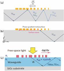
Based on the direct modulation of diffraction channels by localized surface plasmon resonances from metallic nano-structure or Mie scattering from all-dielectric micro/nano-structures, a metagrating emerges as an ideal platform for high-efficiency manipulation of wide-angle diffractive optical fields. In this paper, the physics and applications behind metagrating-based manipulation of diffractive optical fields are reviewed. First, metagratings with desirable high diffraction efficiency are introduced, including different working schemes of reflection and transmission modes as well as symmetric, asymmetric, and reconfigurable configurations. Second, by incorporating the high diffraction metagrating with displacement-coded phase modulation mechanism, arbitrary wavefront shaping with a wide-angle range can be realized, leading to their special applications in high numerical aperture metalens, angle-tunable multi-functional devices, and wide-angle hologram metagratings. Third, considering the metagrating as a bridge to connect the surface wave and free-space wave, the mutual conversion between a free-space wavefront and a surface wavefront is analyzed. Finally, we give a brief summary and the development trend and the potential applications of metagratings are prospected.
Apr. 09, 2021Vol. 41 Issue 8 0823011 (2021)
Lingling Qiao, Min Wang, Rongbo Wu, Zhiwei Fang, Jintian Lin, Wei Chu, and Ya Cheng
Lithium niobate on insulator (LNOI) provides the critical platform for the next-generation photonic integrated circuits demanded by the high-speed optical communications and optical information processing in the future. The recent advances in fabrication of a variety of key photonic structures and devices using LNOI chip manufacturing technology are reviewed. The fabricated LNOI photonic devices are used for demonstrating highly efficient and tunable nonlinear optical processes thanks to the large nonlinear coefficient as well as the strong electro-optic property of monocrystalline LNOI.
Apr. 20, 2021Vol. 41 Issue 8 0823012 (2021)
Shijie Liu, Yuanlin Zheng, and Xianfeng Chen
The lithium niobate crystal is a multifunctional optical material with excellent comprehensive properties. For the past decades, lithium niobate crystal has attracted significant attention in optics researches. Recently, lithium niobate on insulator (LNOI), also known as lithium niobate thin film (LNTF), has been considered as a revolutionary technology in optics that rejuvenates lithium niobate for LNOI-based integrated photonics. A LNTF is irreplaceable in frequency conversion since it is one of the best nonlinear crystals. In this study, we summarize the most recent progress of LNTF in nonlinear frequency conversions, such as second-order nonlinearities, third-order nonlinearities, cascaded nonlinearities, and optical frequency comb. Finally, we present the prospect for photonic integrated circuits (PIC) on the LNOI platform.
Apr. 09, 2021Vol. 41 Issue 8 0823013 (2021)
Xinliang Zhang, and Yanjing Zhao
Optical frequency combs are composed of a series of discrete and equidistant coherent lasers. Optical frequency combs can be used as a high-precision optical frequency scale for accurate measurement of time and frequency. In recent years, microcavity-generated optical frequency combs have attracted significant attention due to their compact footprint, low power consumption, and monolithic integration. The emergence of solitons greatly improves the coherence of microcavity optical frequency combs that are characterized by rich nonlinear physical dynamics and have good application prospects in optical clocks, ultrafast measurements, coherent communication, and other fields. In this article, recent progress of microcavity optical frequency combs is reviewed. Specifically, the theoretical models, generation methods, physical mechanisms, characterizations, and applications of microcavity optical frequency combs are considered. Future trends and perspectives are also discussed. Soliton microcavity optical frequency combs have been considered outstanding candidates in the exploration of next generation optical sources and are expected to lead to revolutionary developments in various fields.
Apr. 09, 2021Vol. 41 Issue 8 0823014 (2021)
Jianfeng Chen, Wenyao Liang, and Zhiyuan Li
Topological photonic state, as a new type of waveguide state with one-way transport, can resist backscattering and is immune to obstacles and defects. Thus, it has found extensive potential applications in topological lasers, quantum information, optical hybrid integrated circuits, nonlinear optics, and other fields owing to its unique properties. In addition, magneto-optical photonic crystal provides an important platform for realizing topological photonic states and exploring their novel physical properties. In this paper, around the progress of topological photonic states in magneto-optic photonic crystals, firstly, we reviewed the topological photonic states in ordered and disordered lattices and revealed the microscopic physical images of topological photonic states. Next, we discussed the topological photonic states in magneto-optical photonic crystals with broken time-reversal and space-reversal symmetries and described the generation of antichiral topological photonic states. Then, we summarized the research on broadband topological photonic states and topological slow-light states and introduced novel topological optical phenomena and device design. Finally, we analyzed the key issues and prospected the future development trends in the study of topological photonic states in magneto-optical photonic crystals.
Apr. 09, 2021Vol. 41 Issue 8 0823015 (2021)
Lieyu Chen, Zhancheng Li, Hua Cheng, Jianguo Tian, and Shuqi Chen
The preparation and manipulation of single-photon and multiphoton quantum states play critical roles in the development and application of the quantum information technology. Based on miniaturization and integration of quantum devices, the effective preparation and manipulation of quantum states are an emerging problem in the quantum information technology field. Metasurfaces, as planar artificial nanostructure arrays, can effectively control the amplitude, phase, and polarization of a light field in sub-wavelength scale, which provide a good methodology for the design of micro-nano optical devices. Recent advances have demonstrated that high-efficiency metasurfaces are a powerful platform for the realization of integrated and miniaturized quantum devices. This paper reviews the design principles and broad applications of high-efficiency metasurfaces in the visible and near-infrared regimes. In addition, this paper discusses recent key metasurface approaches to improve the performance of single-photon emitters and preparation and manipulation of multiphoton entangled states.
Apr. 09, 2021Vol. 41 Issue 8 0823016 (2021)
Zhanghua Han, Kaili Sun, and Yangjian Cai
Terahertz (THz) technology plays a significant role in basic research and industrial applications. However, the wide application of it is still limited by efficient and compact THz sources, especially in the 0.5-2.0 THz band. Currently, researchers have adopted various technologies to generate THz radiations, in which the optical-based methods are the most important means. In this paper, first , for the THz pulse and continuous waves, the THz radiation generation mechanism based on the photoconductivity effect and nonlinear optical difference frequency are summarized with the application of micro-nano optical structures to improve the conversion efficiency from the pump light to THz radiation. Then, two enhancement situations of the metal nano-optical antenna by enhancing the local electric field of the pump light to improve the THz radiation efficiency, and the metal nano-optical antenna as the THz radiation source are analyzed. Finally, the use of other optical micro-nanostructures in the generation of THz radiation have been outlooked, especially the enhancement effect of novel physical phenomena, such as Mie resonance, non-radiative mode and bound state in the continuous domain supported by all-dielectric optical antennas.
Apr. 09, 2021Vol. 41 Issue 8 0823017 (2021)
Linsen Chen, Wen Qiao, Yan Ye, Yanhua Liu, and Donglin Pu
Flexible optoelectronic devices put forward higher requirements for micro-nano fabrication technology, including large-scale, complex surface-relief structure, cross-scale, transparent or flexible substrate, and so on. In this paper, 3D laser direct writing technology and frequency variable interference lithography technology based on phase element modulation are introduced. These fabrication technologies are adopted to pattern complex surface relief structures and pixelated nanostructures, respectively. In addition, the micro-nano additive manufacturing based on structural confined electroplating or coating methods provide environmentally friendly fabrication means for functional materials. Enabled by micro-nano-patterning and structural functionalization platform, novel applications of flexible optoelectronic materials/devices are highlighted. Predictably, micro-nano-manufacturing technology will promote the rapid development of the flexible optoelectronic industry.
Apr. 09, 2021Vol. 41 Issue 8 0823018 (2021)
Mengyu Wang, Yu Yang, Tao Wu, Bin Liu, Yanjun Fu, and Keyi Wang
Compared with glass microcavity, a calcium fluoride (CaF2) crystalline microcavity has the advantages of small absorption coefficient, fewer defects, higher purity, and being insensitive to ambient humidity. It has potential applications in microwave photonics, gyroscopes, and nonlinear optics. In this paper, a spheroid CaF2 millimeter crystalline microcavity is fabricated by the ultra-precision machining technology. To fabricate such a microcavity, a home-made precision machining system is developed. The shape of the fabricated microcavity is a spheroid, and the surface roughness of the edge of the microcavity is as low as 1.97 nm. Efficient coupling between the tapered fiber waveguide and the CaF2 crystalline microcavity is achieved. The coupling system exhibits an ultra-high-quality (Q) factor up to ~10 8 and a free-spectral-range as low as ~0.03 nm. These results demonstrate that the fabrication method for the CaF2 crystalline microcavity is significant, and can promote its applications. The characteristics of CaF2 crystalline microcavity also prove its potential in optical filter, cavity quantum electrodynamics, nonlinear optics, and optical gyroscope.
Apr. 20, 2021Vol. 41 Issue 8 0823019 (2021)
Ying Liu, Jie Fan, Jun Qi, Yonggang Zou, Haizhu Wang, Yongqin Hao, and Xiaohui Ma
Affected by the manufacturing process of gratings, the slight deviation of grating parameters can easily lead the coupling coefficients to deviating from the design values, deteriorating the distributed feedback (DFB) semiconductor lasers. In this paper, the coupling coefficients of lateral asymmetric gratings were analyzed by combining the coupled mode theory in the case of perturbation with numerical simulations. When the ratio of grating width to ridge width is in a certain range, the light fields in the waveguide slightly deviate due to the introduction of the asymmetric distance between two sub-gratings, thus changing the coupling of the light fields. This is beneficial for the coupling coefficients to stabilize in a reasonable range and considerably alleviates the influence of such parameters as duty ratio on the coupling coefficients. Besides, it lowers the influence of errors in the grating process on the properties of DFB semiconductor lasers. Furthermore, the uniform distribution of photon density in the resonator avoids the space hole-burning effect that easily occurs in the conventional grating structure, which is helpful for the output of laser with narrow line width from the semiconductor laser. In conclusion, this work provides a theoretical reference for the design and application of gratings with lateral asynchronous coupling.
Apr. 09, 2021Vol. 41 Issue 8 0823020 (2021)
© Copyright 2018-2021 | Chinese Laser Press.
All Rights Reserved 沪ICP备15018463号-20