


 View fulltext
Advanced Photonics
Co-Editors-in-Chief
Xiao-Cong (Larry) Yuan, Anatoly Zayats
Wenhao Tang, Qing Yang, Hang Xu, Yiyu Guo, Jiqiang Zhang, Chunfang Ouyang, Leixin Meng, and Xu Liu
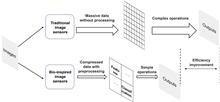
With the rapid development of sensor networks, machine vision faces the problem of storing and computing massive data. The human visual system has a very efficient information sense and computation ability, which has enlightening significance for solving the above problems in machine vision. This review aims to comprehensively summarize the latest advances in bio-inspired image sensors that can be used to improve machine-vision processing efficiency. After briefly introducing the research background, the relevant mechanisms of visual information processing in human visual systems are briefly discussed, including layer-by-layer processing, sparse coding, and neural adaptation. Subsequently, the cases and performance of image sensors corresponding to various bio-inspired mechanisms are introduced. Finally, the challenges and perspectives of implementing bio-inspired image sensors for efficient machine vision are discussed.
Apr. 08, 2024Vol. 6 Issue 2 024001 (2024)
Zong-Lu Che, Chang-Cun Yan, Xue-Dong Wang, and Liang-Sheng Liao
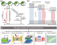
Near-infrared (NIR) light has shown great potential for military and civilian applications owing to its advantages in the composition of sunlight, invisibility to human eyes, deeper penetration into biological tissues, and low optical loss in optical fibers. Therefore, organic optoelectronic materials that can absorb or emit NIR light have aroused great scientific interest in basic science and practical applications. Based on these NIR organic optoelectronic materials, NIR optoelectronic devices have been greatly improved in performance and application. In this review, the representative NIR organic optoelectronic materials used in organic solar cells, organic photodetectors, organic light-emitting diodes, organic lasers, and organic optical waveguide devices are briefly introduced, and the potential applications of each kind of device are briefly summarized. Finally, we summarize and take up the development of NIR organic optoelectronic materials and devices.
Jan. 08, 2024Vol. 6 Issue 1 014001 (2024)
Xuemei Hu, Weizhu Xu, Qingbin Fan, Tao Yue, Feng Yan, Yanqing Lu, and Ting Xu
Metasurface-based imaging has attracted considerable attention owing to its compactness, multifunctionality, and subwavelength coding capability. With the integration of computational imaging techniques, researchers have actively explored the extended capabilities of metasurfaces, enabling a wide range of imaging methods. We present an overview of the recent progress in metasurface-based imaging techniques, focusing on the perspective of computational imaging. Specifically, we categorize and review existing metasurface-based imaging into three main groups, including (i) conventional metasurface design employing canonical methods, (ii) computation introduced independently in either the imaging process or postprocessing, and (iii) an end-to-end computation-optimized imaging system based upon metasurfaces. We highlight the advantages and challenges associated with each computational metasurface-based imaging technique and discuss the potential and future prospects of the computational boosted metaimager.
Feb. 09, 2024Vol. 6 Issue 1 014002 (2024)
Kirill Koshelev, Pavel Tonkaev, and Yuri Kivshar
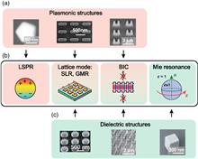
We review the physics and some applications of photonic structures designed for the realization of strong nonlinear chiroptical response. We pay much attention to the recent strategy of utilizing different types of optical resonances in metallic and dielectric subwavelength structures and metasurfaces, including surface plasmon resonances, Mie resonances, lattice-guided modes, and bound states in the continuum. We summarize earlier results and discuss more recent developments for achieving large circular dichroism combined with the high efficiency of nonlinear harmonic generation.
Nov. 08, 2023Vol. 5 Issue 6 064001 (2023)
He-Qi Zheng, Lin Zhang, Yuanjing Cui, and Guodong Qian
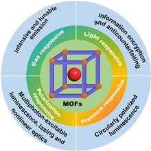
Different from single and static photonic materials, dynamically responsive materials possess numerous advantages, such as being multifunctional, dynamically responsive, and able to provide multiple channels within spatially limited platforms, thus exhibiting great potential for application in the color-on-demand areas, including imaging, optical displays, anticounterfeiting, and encoding. Photonic functional metal–organic frameworks (MOFs), with highly designable framework structures and varieties of optical functional building units, possess broad research and application prospects in the field of photonics, which make it possible to design a promising platform with multifunctional and integrated photonic performance. In this review, beyond the preparation strategies of stimuli-responsive photonic MOFs, we also summarize the stimuli-responsive photonic MOFs regarding several most representative types of external stimuli (such as light, gas, pressure, and polarization). As shown, external stimulation endows the stimuli-responsive photonic MOFs with intriguing regulatable photonic properties: intensive and tunable emission, multiphoton-excitable luminescence, nonlinear optical, circularly polarized luminescence, lasing, etc. Furthermore, their advanced representative applications, such as information encryption and anticounterfeiting display, biological imaging, chemosensing, and others, are also reviewed. The challenges are proposed and the prospects are addressed.
Sep. 06, 2023Vol. 5 Issue 5 054001 (2023)
Zeyang Liu, Danyan Wang, Hao Gao, Moxin Li, Huixian Zhou, and Cheng Zhang
Augmented reality (AR) display, which superimposes virtual images on ambient scene, can visually blend the physical world and the digital world and thus opens a new vista for human–machine interaction. AR display is considered as one of the next-generation display technologies and has been drawing huge attention from both academia and industry. Current AR display systems operate based on a combination of various refractive, reflective, and diffractive optical elements, such as lenses, prisms, mirrors, and gratings. Constrained by the underlying physical mechanisms, these conventional elements only provide limited light-field modulation capability and suffer from issues such as bulky volume and considerable dispersion, resulting in large size, severe chromatic aberration, and narrow field of view of the composed AR display system. Recent years have witnessed the emerging of a new type of optical elements—metasurfaces, which are planar arrays of subwavelength electromagnetic structures that feature an ultracompact footprint and flexible light-field modulation capability, and are widely believed to be an enabling tool for overcoming the limitations faced by current AR displays. Here, we aim to provide a comprehensive review on the recent development of metasurface-enabled AR display technology. We first familiarize readers with the fundamentals of AR display, covering its basic working principle, existing conventional-optics-based solutions, as well as the associated pros and cons. We then introduce the concept of optical metasurfaces, emphasizing typical operating mechanisms, and representative phase modulation methods. We elaborate on three kinds of metasurface devices, namely, metalenses, metacouplers, and metaholograms, which have empowered different forms of AR displays. Their physical principles, device designs, and the performance improvement of the associated AR displays are explained in details. In the end, we discuss the existing challenges of metasurface optics for AR display applications and provide our perspective on future research endeavors.
May. 15, 2023Vol. 5 Issue 3 034001 (2023)

Qiang Luo, Fang Bo, Yongfa Kong, Guoquan Zhang, and Jingjun Xu
Lithium niobate (LN) thin film has received much attention as an integrated photonic platform, due to its rich and great photoelectric characteristics, based on which various functional photonic devices, such as electro-optic modulators and nonlinear wavelength converters, have been demonstrated with impressive performance. As an important part of the integrated photonic system, the long-awaited laser and amplifier on the LN thin-film platform have made a series of breakthroughs and important progress recently. In this review paper, the research progress of lasers and amplifiers realized on lithium niobate thin film platforms is reviewed comprehensively. Specifically, the research progress on optically pumped lasers and amplifiers based on rare-earth ions doping of LN thin films is introduced. Some important parameters and existing limitations of the current development are discussed. In addition, the implementation scheme and research progress of electrically pumped lasers and amplifiers on LN thin-film platforms are summarized. The advantages and disadvantages of optically and electrically pumped LN thin film light sources are analyzed. Finally, the applications of LN thin film lasers and amplifiers and other on-chip functional devices are envisaged.
May. 30, 2023Vol. 5 Issue 3 034002 (2023)
Etienne Brasselet
The optical angular momentum is ubiquitous to the science of light, especially whenever the polarization state and the spatial distribution of the phase are involved, which are most often associated with the spin and orbital parts of the total angular momentum, respectively. Notably, the independent introduction of these two contributions to the total optical angular momentum was accompanied by suggestions regarding the possible detection of their mechanical effects using a torsion pendulum. Today, the classical and quantum mechanical aspects of spin and orbital angular momentum of light and their mutual coupling remain active research topics offering exciting perspectives for photonic technologies. Our brief historical overview shows how the torsion pendulum has accompanied scientific advances on mechanical effects based on the angular degrees of freedom of light since Beth’s pioneering contribution published in 1935.
Jun. 30, 2023Vol. 5 Issue 3 034003 (2023)
Integrated-resonant metadevices: a reviewOn the Cover
Jin Yao, Rong Lin, Mu Ku Chen, and Din Ping Tsai
Integrated-resonant units (IRUs), associating various meta-atoms, resonant modes, and functionalities into one supercell, have been promising candidates for tailoring composite and multifunctional electromagnetic responses with additional degrees of freedom. Integrated-resonant metadevices can overcome many bottlenecks in conventional optical devices, such as broadband achromatism, efficiency enhancement, response selectivity, and continuous tunability, offering great potential for performant and versatile application scenarios. We focus on the recent progress of integrated-resonant metadevices. Starting from the design principle of IRUs, a variety of IRU-based characteristics and subsequent practical applications, including achromatic imaging, light-field sensing, polarization detection, orbital angular momentum generation, metaholography, nanoprinting, color routing, and nonlinear generation, are introduced. Existing challenges in this field and opinions on future research directions are also provided.
Feb. 22, 2023Vol. 5 Issue 2 024001 (2023)
Zhaoyang Sun, Yang Li, Benfeng Bai, Zhendong Zhu, and Hongbo Sun
Kerr frequency combs have been attracting significant interest due to their rich physics and broad applications in metrology, microwave photonics, and telecommunications. In this review, we first introduce the fundamental physics, master equations, simulation methods, and dynamic process of Kerr frequency combs. We then analyze the most promising material platform for realizing Kerr frequency combs—silicon nitride on insulator (SNOI) in comparison with other material platforms. Moreover, we discuss the fabrication methods, process optimization as well as tuning and measurement schemes of SNOI-based Kerr frequency combs. Furthermore, we highlight several emerging applications of Kerr frequency combs in metrology, including spectroscopy, ranging, and timing. Finally, we summarize this review and envision the future development of chip-scale Kerr frequency combs from the viewpoint of theory, material platforms, and tuning methods.
Nov. 14, 2022Vol. 4 Issue 6 064001 (2022)
Trevon Badloe, Seokho Lee, and Junsuk Rho
The explosion in the amount of information that is being processed is prompting the need for new computing systems beyond existing electronic computers. Photonic computing is emerging as an attractive alternative due to performing calculations at the speed of light, the change for massive parallelism, and also extremely low energy consumption. We review the physical implementation of basic optical calculations, such as differentiation and integration, using metamaterials, and introduce the realization of all-optical artificial neural networks. We start with concise introductions of the mathematical principles behind such optical computation methods and present the advantages, current problems that need to be overcome, and the potential future directions in the field. We expect that our review will be useful for both novice and experienced researchers in the field of all-optical computing platforms using metamaterials.
Dec. 21, 2022Vol. 4 Issue 6 064002 (2022)
Pengfei Xu, and Zhiping Zhou
Conventional electronic processors, which are the mainstream and almost invincible hardware for computation, are approaching their limits in both computational power and energy efficiency, especially in large-scale matrix computation. By combining electronic, photonic, and optoelectronic devices and circuits together, silicon-based optoelectronic matrix computation has been demonstrating great capabilities and feasibilities. Matrix computation is one of the few general-purpose computations that have the potential to exceed the computation performance of digital logic circuits in energy efficiency, computational power, and latency. Moreover, electronic processors also suffer from the tremendous energy consumption of the digital transceiver circuits during high-capacity data interconnections. We review the recent progress in photonic matrix computation, including matrix-vector multiplication, convolution, and multiply–accumulate operations in artificial neural networks, quantum information processing, combinatorial optimization, and compressed sensing, with particular attention paid to energy consumption. We also summarize the advantages of silicon-based optoelectronic matrix computation in data interconnections and photonic-electronic integration over conventional optical computing processors. Looking toward the future of silicon-based optoelectronic matrix computations, we believe that silicon-based optoelectronics is a promising and comprehensive platform for disruptively improving general-purpose matrix computation performance in the post-Moore’s law era.
Jul. 06, 2022Vol. 4 Issue 4 044001 (2022)
Milad Gholipour Vazimali, and Sasan Fathpour
Photonics on thin-film lithium niobate (TFLN) has emerged as one of the most pursued disciplines within integrated optics. Ultracompact and low-loss optical waveguides and related devices on this modern material platform have rejuvenated the traditional and commercial applications of lithium niobate for optical modulators based on the electro-optic effect, as well as optical wavelength converters based on second-order nonlinear effects, e.g., second-harmonic, sum-, and difference-frequency generations. TFLN has also created vast opportunities for applications and integrated solutions for optical parametric amplification and oscillation, cascaded nonlinear effects, such as low-harmonic generation; third-order nonlinear effects, such as supercontinuum generation; optical frequency comb generation and stabilization; and nonclassical nonlinear effects, such as spontaneous parametric downconversion for quantum optics. Recent progress in nonlinear integrated photonics on TFLN for all these applications, their current trends, and future opportunities and challenges are reviewed.
May. 30, 2022Vol. 4 Issue 3 034001 (2022)
Haoyi Yu, Qiming Zhang, Xi Chen, Haitao Luan, and Min Gu
The creation of biomimetic neuron interfaces (BNIs) has become imperative for different research fields from neural science to artificial intelligence. BNIs are two-dimensional or three-dimensional (3D) artificial interfaces mimicking the geometrical and functional characteristics of biological neural networks to rebuild, understand, and improve neuronal functions. The study of BNI holds the key for curing neuron disorder diseases and creating innovative artificial neural networks (ANNs). To achieve these goals, 3D direct laser writing (DLW) has proven to be a powerful method for BNI with complex geometries. However, the need for scaled-up, high speed fabrication of BNI demands the integration of DLW techniques with ANNs. ANNs, computing algorithms inspired by biological neurons, have shown their unprecedented ability to improve efficiency in data processing. The integration of ANNs and DLW techniques promises an innovative pathway for efficient fabrication of large-scale BNI and can also inspire the design and optimization of novel BNI for ANNs. This perspective reviews advances in DLW of BNI and discusses the role of ANNs in the design and fabrication of BNI.
Jun. 07, 2022Vol. 4 Issue 3 034002 (2022)
Advances in lithium niobate photonics: development status and perspectivesArticle Video , On the Cover
Guanyu Chen, Nanxi Li, Jun Da Ng, Hong-Lin Lin, Yanyan Zhou, Yuan Hsing Fu, Lennon Yao Ting Lee, Yu Yu, Ai-Qun Liu, and Aaron J. Danner
Lithium niobate (LN) has experienced significant developments during past decades due to its versatile properties, especially its large electro-optic (EO) coefficient. For example, bulk LN-based modulators with high speeds and a superior linearity are widely used in typical fiber-optic communication systems. However, with ever-increasing demands for signal transmission capacity, the high power and large size of bulk LN-based devices pose great challenges, especially when one of its counterparts, integrated silicon photonics, has experienced dramatic developments in recent decades. Not long ago, high-quality thin-film LN on insulator (LNOI) became commercially available, which has paved the way for integrated LN photonics and opened a hot research area of LN photonics devices. LNOI allows a large refractive index contrast, thus light can be confined within a more compact structure. Together with other properties of LN, such as nonlinear/acousto-optic/pyroelectric effects, various kinds of high-performance integrated LN devices can be demonstrated. A comprehensive summary of advances in LN photonics is provided. As LN photonics has experienced several decades of development, our review includes some of the typical bulk LN devices as well as recently developed thin film LN devices. In this way, readers may be inspired by a complete picture of the evolution of this technology. We first introduce the basic material properties of LN and several key processing technologies for fabricating photonics devices. After that, various kinds of functional devices based on different effects are summarized. Finally, we give a short summary and perspective of LN photonics. We hope this review can give readers more insight into recent advances in LN photonics and contribute to the further development of LN related research.
Jun. 08, 2022Vol. 4 Issue 3 034003 (2022)
Jaekyung Kim, Junhwa Seong, Younghwan Yang, Seong-Won Moon, Trevon Badloe, and Junsuk Rho
Metasurfaces have attracted great attention due to their ability to manipulate the phase, amplitude, and polarization of light in a compact form. Tunable metasurfaces have been investigated recently through the integration with mechanically moving components and electrically tunable elements. Two interesting applications, in particular, are to vary the focal point of metalenses and to switch between holographic images. We present the recent progress on tunable metasurfaces focused on metalenses and metaholograms, including the basic working principles, advantages, and disadvantages of each working mechanism. We classify the tunable stimuli based on the light source and electrical bias, as well as others such as thermal and mechanical modulation. We conclude by summarizing the recent progress of metalenses and metaholograms, and providing our perspectives for the further development of tunable metasurfaces.
Mar. 07, 2022Vol. 4 Issue 2 024001 (2022)
Lingqi Li, Weijin Kong, and Feng Chen
Femtosecond laser inscription or writing has been recognized as a powerful technique to engineer various materials toward a number of applications. By efficient modification of refractive indices of dielectric crystals, optical waveguides with diverse configurations have been produced by femtosecond laser writing. The waveguiding properties depend not only on the parameters of the laser writing but also on the nature of the crystals. The mode profile tailoring and polarization engineering are realizable by selecting appropriate fabrication conditions. In addition, regardless of the complexity of crystal refractive index changes induced by ultrafast pulses, several three-dimensional geometries have been designed and implemented that are useful for the fabrication of laser-written photonic chips. Some intriguing devices, e.g., waveguide lasers, wavelength converters, and quantum memories, have been made, exhibiting potential for applications in various areas. Our work gives a concise review of the femtosecond laser-inscribed waveguides in dielectric crystals and focuses on the recent advances of this research area, including the fundamentals, fabrication, and selected photonic applications.
Mar. 29, 2022Vol. 4 Issue 2 024002 (2022)
Jianyu Zhang, Xueqian Zhao, Hanchen Shen, Jacky W. Y. Lam, Haoke Zhang, and Ben Zhong Tang
White light, which contains polychromic visible components, affects the rhythm of organisms and has the potential for advanced applications of lighting, display, and communication. Compared with traditional incandescent bulbs and inorganic diodes, pure organic materials are superior in terms of better compatibility, flexibility, structural diversity, and environmental friendliness. In the past few years, polychromic emission has been obtained based on organic aggregates, which provides a platform to achieve white-light emission. Several white-light emitters are sporadically reported, but the underlying mechanistic picture is still not fully established. Based on these considerations, we will focus on the single-component and multicomponent strategies to achieve efficient white-light emission from pure organic aggregates. Thereinto, single-component strategy is introduced from four parts: dual fluorescence, fluorescence and phosphorescence, dual phosphorescence with anti-Kasha’s behavior, and clusteroluminescence. Meanwhile, doping, supramolecular assembly, and cocrystallization are summarized as strategies for multicomponent systems. Beyond the construction strategies of white-light emitters, their advanced representative applications, such as organic light-emitting diodes, white luminescent dyes, circularly polarized luminescence, and encryption, are also prospected. It is expected that this review will draw a comprehensive picture of white-light emission from organic aggregates as well as their emerging applications.
Dec. 30, 2021Vol. 4 Issue 1 014001 (2022)
Emanuele Galiffi, Romain Tirole, Shixiong Yin, Huanan Li, Stefano Vezzoli, Paloma A. Huidobro, Mário G. Silveirinha, Riccardo Sapienza, Andrea Alù, and J. B. Pendry
Time-varying media have recently emerged as a new paradigm for wave manipulation, due to the synergy between the discovery of highly nonlinear materials, such as epsilon-near-zero materials, and the quest for wave applications, such as magnet-free nonreciprocity, multimode light shaping, and ultrafast switching. In this review, we provide a comprehensive discussion of the recent progress achieved with photonic metamaterials whose properties stem from their modulation in time. We review the basic concepts underpinning temporal switching and its relation with spatial scattering and deploy the resulting insight to review photonic time-crystals and their emergent research avenues, such as topological and non-Hermitian physics. We then extend our discussion to account for spatiotemporal modulation and its applications to nonreciprocity, synthetic motion, giant anisotropy, amplification, and many other effects. Finally, we conclude with a review of the most attractive experimental avenues recently demonstrated and provide a few perspectives on emerging trends for future implementations of time-modulation in photonics.
Feb. 14, 2022Vol. 4 Issue 1 014002 (2022)
Jian Chen, Chenhao Wan, and Qiwen Zhan
Structured light with inhomogeneous phase, amplitude, and polarization spatial distributions that represent an infinite-dimensional space of eigenstates for light as the ideal carrier can provide a structured combination of photonic spin and orbital angular momentum (OAM). Photonic spin angular momentum (SAM) interactions with matter have long been studied, whereas the photonic OAM has only recently been discovered, receiving attention in the past three decades. Although controlling polarization (i.e., SAM) alone can provide useful information about the media with which the light interacts, light fields carrying both OAM and SAM may provide additional information, permitting new sensing mechanisms and light–matter interactions. We summarize recent developments in controlling photonic angular momentum (AM) using complex structured optical fields. Arbitrarily oriented photonic SAM and OAM states may be generated through careful engineering of the spatial and temporal structures of optical fields. Moreover, we discuss potential applications of specifically engineered photonic AM states in optical tweezers, directional coupling, and optical information transmission and processing.
Nov. 17, 2021Vol. 3 Issue 6 064001 (2021)
Xiaojiong Chen, Zhaorong Fu, Qihuang Gong, and Jianwei Wang
Entanglement is one of the most vital properties of quantum mechanical systems, and it forms the backbone of quantum information technologies. Taking advantage of nano/microfabrication and particularly complementary metal-oxide-semiconductor manufacturing technologies, photonic integrated circuits (PICs) have emerged as a versatile platform for the generation, manipulation, and measurement of entangled photonic states. We summarize the recent progress of quantum entanglement on PICs, starting from the generation of nonentangled and entangled biphoton states, to the generation of entangled states of multiple photons, multiple dimensions, and multiple degrees of freedom, as well as their applications for quantum information processing.
Dec. 07, 2021Vol. 3 Issue 6 064002 (2021)
Stefania Castelletto, and Alberto Boretti
Solid-state atomic-sized color centers in wide-band-gap semiconductors, such as diamond, silicon carbide, and hexagonal boron nitride, are important platforms for quantum technologies, specifically for single-photon sources and quantum sensing. One of the emerging applications of these quantum emitters is subdiffraction imaging. This capability is provided by the specific photophysical properties of color centers, such as high dipole moments, photostability, and a variety of spectral ranges of the emitters with associated optical and microwave control of their quantum states. We review applications of color centers in traditional super-resolution microscopy and quantum imaging methods, and compare relative performance. The current state and perspectives of their applications in biomedical, chemistry, and material science imaging are outlined.
Sep. 13, 2021Vol. 3 Issue 5 054001 (2021)
Jongchan Park, David J. Brady, Guoan Zheng, Lei Tian, and Liang Gao
Optical imaging has served as a primary method to collect information about biosystems across scales—from functionalities of tissues to morphological structures of cells and even at biomolecular levels. However, to adequately characterize a complex biosystem, an imaging system with a number of resolvable points, referred to as a space-bandwidth product (SBP), in excess of one billion is typically needed. Since a gigapixel-scale far exceeds the capacity of current optical imagers, compromises must be made to obtain either a low spatial resolution or a narrow field-of-view (FOV). The problem originates from constituent refractive optics—the larger the aperture, the more challenging the correction of lens aberrations. Therefore, it is impractical for a conventional optical imaging system to achieve an SBP over hundreds of millions. To address this unmet need, a variety of high-SBP imagers have emerged over the past decade, enabling an unprecedented resolution and FOV beyond the limit of conventional optics. We provide a comprehensive survey of high-SBP imaging techniques, exploring their underlying principles and applications in bioimaging.
Jun. 26, 2021Vol. 3 Issue 4 044001 (2021)
Yan Jin, Lin Zhou, Jie Liang, and Jia Zhu
Dynamic plasmonics with the real-time active control capability of plasmonic resonances attracts much interest in the communities of physics, chemistry, and material science. Among versatile reconfigurable strategies for dynamic plasmonics, electrochemically driven strategies have garnered most of the attention. We summarize three primary strategies to enable electrochemically dynamic plasmonics, including structural transformation, carrier-density modulation, and electrochemically active surrounding-media manipulation. The reconfigurable microstructures, optical properties, and underlying physical mechanisms are discussed in detail. We also summarize the most promising applications of dynamic plasmonics, including smart windows, structural color displays, and chemical sensors. We suggest more research efforts toward the widespread applications of dynamic plasmonics.
Jun. 30, 2021Vol. 3 Issue 4 044002 (2021)
Optical trapping with structured light: a reviewArticle Video , EIC Choice Award
Yuanjie Yang, Yu-Xuan Ren, Mingzhou Chen, Yoshihiko Arita, and Carmelo Rosales-Guzmán
Optical trapping describes the interaction between light and matter to manipulate micro-objects through momentum transfer. In the case of 3D trapping with a single beam, this is termed optical tweezers. Optical tweezers are a powerful and noninvasive tool for manipulating small objects, and have become indispensable in many fields, including physics, biology, soft condensed matter, among others. In the early days, optical trapping was typically accomplished with a single Gaussian beam. In recent years, we have witnessed rapid progress in the use of structured light beams with customized phase, amplitude, and polarization in optical trapping. Unusual beam properties, such as phase singularities on-axis and propagation invariant nature, have opened up novel capabilities to the study of micromanipulation in liquid, air, and vacuum. We summarize the recent advances in the field of optical trapping using structured light beams.
May. 17, 2021Vol. 3 Issue 3 034001 (2021)
Zhiping Hu, Zhengzheng Liu, Zijun Zhan, Tongchao Shi, Juan Du, Xiaosheng Tang, and Yuxin Leng
In the past decade, lead halide perovskites have emerged as potential optoelectronic materials in the fields of light-emitting diode, solar cell, photodetector, and laser, due to their low-cost synthesis method, tunable bandgap, high quantum yield, large absorption, gain coefficient, and low trap-state densities. In this review, we present a comprehensive discussion of lead halide perovskite applications, with an emphasis on recent advances in synthetic strategies, morphology control, and lasing performance. In particular, the synthetic strategies of solution and vapor progress and the morphology control of perovskite nanocrystals are reviewed. Furthermore, we systematically discuss the latest development of perovskite laser with various fundamental performances, which are highly dependent on the dimension and size of nanocrystals. Finally, considering current challenges and perspectives on the development of lead halide perovskite nanocrystals, we provide an outlook on achieving high-quality lead perovskite lasers and expanding their practical applications.
Jun. 02, 2021Vol. 3 Issue 3 034002 (2021)
Dandan Wen, Jasper J. Cadusch, Jiajun Meng, and Kenneth B. Crozier
Multicolor holography can faithfully record the color, depth, parallax, and other properties of scenes and have thus found numerous applications, for example, in optical document security, nonvolatile data storage, and virtual or augmented reality systems. Nanophotonic metasurfaces present multiple degrees of freedom to manipulate the properties of optical fields at visible wavelengths. These in turn provide opportunities for metasurface-based multicolor holography. We describe recent developments in multicolor metasurface holograms. These are categorized based on their color-separating mechanisms rather than their structural properties, such as whether they are plasmonic or dielectric. We hope this review will provide readers with new insights and thus help extend applications of metasurface-based multicolor holography to other fields.
Feb. 26, 2021Vol. 3 Issue 2 024001 (2021)
Dezhi Tan, Zhuo Wang, Beibei Xu, and Jianrong Qiu
Integrated photonics is attracting considerable attention and has found many applications in both classical and quantum optics, fulfilling the requirements for the ever-growing complexity in modern optical experiments and big data communication. Femtosecond (fs) laser direct writing (FLDW) is an acknowledged technique for producing waveguides (WGs) in transparent glass that have been used to construct complex integrated photonic devices. FLDW possesses unique features, such as three-dimensional fabrication geometry, rapid prototyping, and single step fabrication, which are important for integrated communication devices and quantum photonic and astrophotonic technologies. To fully take advantage of FLDW, considerable efforts have been made to produce WGs over a large depth with low propagation loss, coupling loss, bend loss, and highly symmetrical mode field. We summarize the improved techniques as well as the mechanisms for writing high-performance WGs with controllable morphology of cross-section, highly symmetrical mode field, low loss, and high processing uniformity and efficiency, and discuss the recent progress of WGs in photonic integrated devices for communication, topological physics, quantum information processing, and astrophotonics. Prospective challenges and future research directions in this field are also pointed out.
Mar. 10, 2021Vol. 3 Issue 2 024002 (2021)
Abdul Rahim, Artur Hermans, Benjamin Wohlfeil, Despoina Petousi, Bart Kuyken, Dries Van Thourhout, and Roel Baets
Optical links are moving to higher and higher transmission speeds while shrinking to shorter and shorter ranges where optical links are envisaged even at the chip scale. The scaling in data speed and span of the optical links demands modulators to be concurrently performant and cost-effective. Silicon photonics (SiPh), a photonic integrated circuit technology that leverages the fabrication sophistication of complementary metal-oxide-semiconductor technology, is well-positioned to deliver the performance, price, and manufacturing volume for the high-speed modulators of future optical communication links. SiPh has relied on the plasma dispersion effect, either in injection, depletion, or accumulation mode, to demonstrate efficient high-speed modulators. The high-speed plasma dispersion silicon modulators have been commercially deployed and have demonstrated excellent performance. Recent years have seen a paradigm shift where the integration of various electro-refractive and electro-absorptive materials has opened up additional routes toward performant SiPh modulators. These modulators are in the early years of their development. They promise to extend the performance beyond the limits set by the physical properties of silicon. The focus of our study is to provide a comprehensive review of contemporary (i.e., plasma dispersion modulators) and new modulator implementations that involve the integration of novel materials with SiPh.
Apr. 29, 2021Vol. 3 Issue 2 024003 (2021)
Yanling Zhuang, Xiuli Ren, Xueting Che, Shujuan Liu, Wei Huang, and Qiang Zhao
Organic photoresponsive materials can undergo various reversible variations in certain physical and chemical properties, such as optical properties, electrochemical properties, conformation, and conductivity, upon photoirradiation. They have been widely applied in various optoelectronic fields, especially in information storage. We summarize research progress on organic photoresponsive materials for information storage. First, the design strategies and photoswitching mechanisms for various kinds of organic photoresponsive materials, including small organic molecules, metal complexes, polymers, supramolecules, and cholesteric liquid crystals, are systematically summarized. These materials exhibit reversible changes of absorption and/or emission properties in response to different wavelengths of light. Subsequently, the applications of these organic materials in information storage, such as data (re)writing and erasing, encryption and decryption, and anticounterfeiting, are introduced in detail. Finally, the current challenges and future directions in this rapidly growing research field are discussed. The review will provide important guidance on the future works about the design of excellent organic photoresponsive materials for optoelectronic applications.
Dec. 08, 2020Vol. 3 Issue 1 014001 (2021)
Dong Mao, Yang Zheng, Chao Zeng, Hua Lu, Cong Wang, Han Zhang, Wending Zhang, Ting Mei, and Jianlin Zhao
Cylindrical vector beams and vortex beams, two types of typical singular optical beams characterized by axially symmetric polarization and helical phase front, possess the unique focusing property and the ability of carrying orbital angular momentum. We discuss the formation mechanisms of such singular beams in few-mode fibers under the vortex basis and show recent advances in generating techniques that are mainly based on long-period fiber gratings, mode-selective couplers, offset-spliced fibers, and tapered fibers. The performances of cylindrical vector beams and vortex beams generated in fibers and fiber lasers are summarized and compared to give a comprehensive understanding of singular beams and to promote their practical applications.
Jan. 01, 2021Vol. 3 Issue 1 014002 (2021)
Yifeng Xiong, and Fei Xu
The flat endface of an optical fiber tip is an emerging light-coupled microscopic platform that combines fiber optics with planar micro- and nanotechnologies. Since different materials and structures are integrated onto the endfaces, optical fiber tip devices have miniature sizes, diverse integrated functions, and low insertion losses, making them suitable for all-optical networks. In recent decades, the increasing demand for multifunctional optical fibers has created opportunities to develop various structures on fiber tips. Meanwhile, the unconventional shape of optical fibers presents challenges involving the adaptation of standard planar micro- and nanostructure preparation strategies for fiber tips. In this context, researchers are committed to exploring and optimizing fiber tip manufacturing techniques, thereby paving the way for future integrated all-fiber devices with multifunctional applications. First, we present a broad overview of current fabrication technologies, classified as “top-down,” “bottom-up,” and “material transfer” methods, for patterning optical fiber tips. Next, we review typical structures integrated on fiber tips and their known and potential applications, categorized with respect to functional structure configurations, including “optical functionalization” and “electrical integration.” Finally, we discuss the prospects for future opportunities involving multifunctional integrated fiber tips.
Nov. 04, 2020Vol. 2 Issue 6 064001 (2020)
Zengle Cao, Fengrui Hu, Chunfeng Zhang, Shining Zhu, Min Xiao, and Xiaoyong Wang
Semiconductor perovskite films are now being widely investigated as light harvesters in solar cells with ever-increasing power conversion efficiencies, which have motivated the fabrication of other optoelectronic devices, such as light-emitting diodes, lasers, and photodetectors. Their superior material and optical properties are shared by the counterpart colloidal nanocrystals (NCs), with the additional advantage of quantum confinement that can yield size-dependent optical emission ranging from the near-UV to near-infrared wavelengths. So far, intensive research efforts have been devoted to the optical characterization of perovskite NC ensembles, revealing not only fundamental exciton relaxation and recombination dynamics but also low-threshold amplified spontaneous emission and novel superfluorescence effects. Meanwhile, the application of single-particle spectroscopy techniques to perovskite NCs has helped to resolve a variety of optical properties for which there are few equivalents in traditional colloidal NCs, mainly including nonblinking photoluminescence, suppressed spectral diffusion, stable exciton fine structures, and coherent single-photon emission. While the main purpose of ensemble optical studies is to guide the smooth development of perovskite NCs in classical optoelectronic applications, the rich observations from single-particle optical studies mark the emergence of a potential platform that can be exploited for quantum information technologies.
Sep. 21, 2020Vol. 2 Issue 5 054001 (2020)
Mark I. Stockman
A history and a glimpse into the future of spaser (acronym for “surface plasmon amplification by stimulated emission of radiation”) is provided. The spaser (also called a plasmonic nanolaser) is an active nanosystem including a gain medium and a nanoplasmonic metal core. It generates coherent intense nanolocalized fields. Theoretically predicted in 2003 by Bergman and Stockman, the spaser grew into a large fundamental research and application field with thousands of publications. We review a few of them to illustrate the most important and general fundamental properties of the spaser. We also review some selected applications of spasers, in particular, to ultrasensing and biomedical problems, concentrating on cancer-cell theranostics (therapeutics and diagnostics). In conclusion, we attempt to glimpse into the future by predicting that the next big development of the spasers will be topological nano-optics, and its “killer” application will be ultrafast, high-density on-chip communications for future information processing.
Oct. 30, 2020Vol. 2 Issue 5 054002 (2020)
Tengfei Hao, Yanzhong Liu, Jian Tang, Qizhuang Cen, Wei Li, Ninghua Zhu, Yitang Dai, José Capmany, Jianping Yao, and Ming Li
An optoelectronic oscillator (OEO) is a microwave photonic system that produces microwave signals with ultralow phase noise using a high-quality-factor optical energy storage element. This type of oscillator is desired in various practical applications, such as communication links, signal processing, radar, metrology, radio astronomy, and reference clock distribution. Recently, new mode control and selection methods based on Fourier domain mode-locking and parity-time symmetry have been proposed and experimentally demonstrated in OEOs, which overcomes the long-existing mode building time and mode selection problems in a traditional OEO. Due to these mode control and selection methods, continuously chirped microwave waveforms can be generated directly from the OEO cavity and single-mode operation can be achieved without the need of ultranarrowband filters, which are not possible in a traditional OEO. Integrated OEOs with a compact size and low power consumption have also been demonstrated, which are key steps toward a new generation of compact and versatile OEOs for demanding applications. We review recent progress in the field of OEOs, with particular attention to new mode control and selection methods, as well as chip-scale integration of OEOs.
Jul. 25, 2020Vol. 2 Issue 4 044001 (2020)
Weiqiang Wang, Leiran Wang, and Wenfu Zhang
Optical frequency combs, a revolutionary light source characterized by discrete and equally spaced frequencies, are usually regarded as a cornerstone for advanced frequency metrology, precision spectroscopy, high-speed communication, distance ranging, molecule detection, and many others. Due to the rapid development of micro/nanofabrication technology, breakthroughs in the quality factor of microresonators enable ultrahigh energy buildup inside cavities, which gives birth to microcavity-based frequency combs. In particular, the full coherent spectrum of the soliton microcomb (SMC) provides a route to low-noise ultrashort pulses with a repetition rate over two orders of magnitude higher than that of traditional mode-locking approaches. This enables lower power consumption and cost for a wide range of applications. This review summarizes recent achievements in SMCs, including the basic theory and physical model, as well as experimental techniques for single-soliton generation and various extraordinary soliton states (soliton crystals, Stokes solitons, breathers, molecules, cavity solitons, and dark solitons), with a perspective on their potential applications and remaining challenges.
Jun. 19, 2020Vol. 2 Issue 3 034001 (2020)
Yufeng Song, Zhenhong Wang, Cong Wang, Krassimir Panajotov, and Han Zhang
Rogue waves (RWs) are rare, extreme amplitude, localized wave packets, which have received much interest recently in different areas of physics. Fiber lasers with their abundant nonlinear dynamics provide an ideal platform to observe optical RW formation. We review recent research progress on rogue waves in fiber lasers. Basic concepts of RWs and the mechanisms of RW generation in fiber lasers are discussed, along with representative experimental and theoretical results. The measurement methods for RW identification in fiber lasers are presented and analyzed. Finally, prospects for future RW research in fiber lasers are summarized.
Apr. 09, 2020Vol. 2 Issue 2 024001 (2020)
Kang Lin, Ilia Tutunnikov, Junyang Ma, Junjie Qiang, Lianrong Zhou, Olivier Faucher, Yehiam Prior, Ilya Sh. Averbukh, and Jian Wu
Molecular alignment and orientation by laser fields has attracted significant attention in recent years, mostly due to new capabilities to manipulate the molecular spatial arrangement. Molecules can now be efficiently prepared for ionization, structural imaging, orbital tomography, and more, enabling, for example, shooting of dynamic molecular movies. Furthermore, molecular alignment and orientation processes give rise to fundamental quantum and classical phenomena like quantum revivals, Anderson localization, and rotational echoes, just to mention a few. We review recent progress on the visualization, coherent control, and applications of the rich dynamics of molecular rotational wave packets driven by laser pulses of various intensities, durations, and polarizations. In particular, we focus on the molecular unidirectional rotation and its visualization, the orientation of chiral molecules, and the three-dimensional orientation of asymmetric-top molecules. Rotational echoes are discussed as an example of nontrivial dynamics and detection of prepared molecular states.
Apr. 11, 2020Vol. 2 Issue 2 024002 (2020)
Terahertz surface plasmonic waves: a reviewArticle Video
Xueqian Zhang, Quan Xu, Lingbo Xia, Yanfeng Li, Jianqiang Gu, Zhen Tian, Chunmei Ouyang, Jiaguang Han, and Weili Zhang
Terahertz science and technology promise many cutting-edge applications. Terahertz surface plasmonic waves that propagate at metal–dielectric interfaces deliver a potentially effective way to realize integrated terahertz devices and systems. Previous concerns regarding terahertz surface plasmonic waves have been based on their highly delocalized feature. However, recent advances in plasmonics indicate that the confinement of terahertz surface plasmonic waves, as well as their propagating behaviors, can be engineered by designing the surface environments, shapes, structures, materials, etc., enabling a unique and fascinating regime of plasmonic waves. Together with the essential spectral property of terahertz radiation, as well as the increasingly developed materials, microfabrication, and time-domain spectroscopy technologies, devices and systems based on terahertz surface plasmonic waves may pave the way toward highly integrated platforms for multifunctional operation, implementation, and processing of terahertz waves in both fundamental science and practical applications. We present a review on terahertz surface plasmonic waves on various types of supports in a sequence of properties, excitation and detection, and applications. The current research trend and outlook of possible research directions for terahertz surface plasmonic waves are also outlined.
Jan. 07, 2020Vol. 2 Issue 1 014001 (2020)
Yang Yu, Ting-Hui Xiao, Yunzhao Wu, Wanjun Li, Qing-Guang Zeng, Li Long, and Zhi-Yuan Li
In the near future, single-molecule surface-enhanced Raman spectroscopy (SERS) is expected to expand the family of popular analytical tools for single-molecule characterization. We provide a roadmap for achieving single molecule SERS through different enhancement strategies for diverse applications. We introduce some characteristic features related to single-molecule SERS, such as Raman enhancement factor, intensity fluctuation, and data analysis. We then review recent strategies for enhancing the Raman signal intensities of single molecules, including electromagnetic enhancement, chemical enhancement, and resonance enhancement strategies. To demonstrate the utility of single-molecule SERS in practical applications, we present several examples of its use in various fields, including catalysis, imaging, and nanoelectronics. Finally, we specify current challenges in the development of single-molecule SERS and propose corresponding solutions.
Feb. 26, 2020Vol. 2 Issue 1 014002 (2020)
Dalong Qi, Shian Zhang, Chengshuai Yang, Yilin He, Fengyan Cao, Jiali Yao, Pengpeng Ding, Liang Gao, Tianqing Jia, Jinyang Liang, Zhenrong Sun, and Lihong V. Wang
Compressed ultrafast photography (CUP) is a burgeoning single-shot computational imaging technique that provides an imaging speed as high as 10 trillion frames per second and a sequence depth of up to a few hundred frames. This technique synergizes compressed sensing and the streak camera technique to capture nonrepeatable ultrafast transient events with a single shot. With recent unprecedented technical developments and extensions of this methodology, it has been widely used in ultrafast optical imaging and metrology, ultrafast electron diffraction and microscopy, and information security protection. We review the basic principles of CUP, its recent advances in data acquisition and image reconstruction, its fusions with other modalities, and its unique applications in multiple research fields.
Feb. 28, 2020Vol. 2 Issue 1 014003 (2020)
Daniel J. Brod, Ernesto F. Galvão, Andrea Crespi, Roberto Osellame, Nicolò Spagnolo, and Fabio Sciarrino
Boson sampling is a computational problem that has recently been proposed as a candidate to obtain an unequivocal quantum computational advantage. The problem consists in sampling from the output distribution of indistinguishable bosons in a linear interferometer. There is strong evidence that such an experiment is hard to classically simulate, but it is naturally solved by dedicated photonic quantum hardware, comprising single photons, linear evolution, and photodetection. This prospect has stimulated much effort resulting in the experimental implementation of progressively larger devices. We review recent advances in photonic boson sampling, describing both the technological improvements achieved and the future challenges. We also discuss recent proposals and implementations of variants of the original problem, theoretical issues occurring when imperfections are considered, and advances in the development of suitable techniques for validation of boson sampling experiments. We conclude by discussing the future application of photonic boson sampling devices beyond the original theoretical scope.
May. 09, 2019Vol. 1 Issue 3 034001 (2019)
Weiqiang Ding, Tongtong Zhu, Lei-Ming Zhou, and Cheng-Wei Qiu
Usually, an unfocused light beam, such as a paraxial Gaussian beam, can exert a force on an object along the direction of light propagation, which is known as light pressure. Recently, however, it was found that an unfocused light beam can also exert an optical pulling force (OPF) on an object toward the source direction; the beam is accordingly named an optical tractor beam. In recent years, this intriguing force has attracted much attention and a huge amount of progress has been made both in theory and experiment. We briefly review recent progress achieved on this topic. We classify the mechanisms to achieve an OPF into four different kinds according to the dominant factors. The first one is tailoring the incident beam. The second one is engineering the object’s optical parameters. The third one is designing the structured material background, in which the light–matter interaction occurs, and the fourth one is utilizing the indirect photophoretic force, which is related to the thermal effect of light absorption. For all the methods, we analyze the basic principles and review the recent achievements. Finally, we also give a brief conclusion and an outlook on the future development of this field.
Mar. 27, 2019Vol. 1 Issue 2 024001 (2019)
Basudeb Sain, Cedrik Meier, and Thomas Zentgraf
Free from phase-matching constraints, plasmonic metasurfaces have contributed significantly to the control of optical nonlinearity and enhancement of nonlinear generation efficiency by engineering subwavelength meta-atoms. However, high dissipative losses and inevitable thermal heating limit their applicability in nonlinear nanophotonics. All-dielectric metasurfaces, supporting both electric and magnetic Mie-type resonances in their nanostructures, have appeared as a promising alternative to nonlinear plasmonics. High-index dielectric nanostructures, allowing additional magnetic resonances, can induce magnetic nonlinear effects, which, along with electric nonlinearities, increase the nonlinear conversion efficiency. In addition, low dissipative losses and high damage thresholds provide an extra degree of freedom for operating at high pump intensities, resulting in a considerable enhancement of the nonlinear processes. We discuss the current state of the art in the intensely developing area of all-dielectric nonlinear nanostructures and metasurfaces, including the role of Mie modes, Fano resonances, and anapole moments for harmonic generation, wave mixing, and ultrafast optical switching. Furthermore, we review the recent progress in the nonlinear phase and wavefront control using all-dielectric metasurfaces. We discuss techniques to realize all-dielectric metasurfaces for multifunctional applications and generation of second-order nonlinear processes from complementary metal–oxide–semiconductor-compatible materials.
Apr. 03, 2019Vol. 1 Issue 2 024002 (2019)
Jingjing Zhang, John B. Pendry, and Yu Luo
Transformation optics is a mathematical method that is based on the geometric interpretation of Maxwell’s equations. This technique enables a direct link between a desired electromagnetic (EM) phenomenon and the material response required for its occurrence, providing a powerful and intuitive design tool for the control of EM fields on all length scales. With the unprecedented design flexibility offered by transformation optics (TO), researchers have demonstrated a host of interesting devices, such as invisibility cloaks, field concentrators, and optical illusion devices. Recently, the applications of TO have been extended to the subwavelength scale to study surface plasmon-assisted phenomena, where a general strategy has been suggested to design and study analytically various plasmonic devices and investigate the associated phenomena, such as nonlocal effects, Casimir interactions, and compact dimensions. We review the basic concept of TO and its advances from macroscopic to the nanoscale regimes.
Jan. 28, 2019Vol. 1 Issue 1 014001 (2019)
Cun-Zheng Ning
Semiconductor lasers, an important subfield of semiconductor photonics, have fundamentally changed many aspects of our lives and enabled many technologies since their creation in the 1960s. As in other semiconductor-based fields, such as microelectronics, miniaturization has been a constant theme, with nanolasers being an important frontier of research over the last decade. We review the progress, existing issues, and future prospects of nanolasers, especially in relation to their potential application in chip-scale optical interconnects. One of the important challenges in this application is minimizing the size and energy consumption of nanolasers. We begin with the application background of this challenge and then compare basic features of various semiconductor lasers. We present existing issues with nanolasers and discuss potential solutions to meet the size and energy-efficiency challenge. Our discussions cover a broad range of miniaturized lasers, including plasmonic nanolasers and lasers with two-dimensional monolayer gain materials, with focus on near-infrared wavelengths.
Jan. 28, 2019Vol. 1 Issue 1 014002 (2019)
© Copyright 2018-2021 | Chinese Laser Press.
All Rights Reserved 沪ICP备15018463号-20