


Please enter the answer below before you can view the full text.

2025
Volume: 52 Issue 5
20 Article(s)

Minghao Li, Weinan Xu, Jichao Yan, Xinchen Zhang, Yunpeng Xu, Zihan Zang, Mukun He, Jizhe Zhao, Bin Zhang, Changzheng Sun, Zhibiao Hao, Bing Xiong, Yanjun Han, Jian Wang, Hongtao Li, Lin Gan, Lai Wang, and Yi Luo
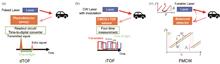
SignificanceWith the advancement of artificial intelligence and automation technologies, intelligent devices that require enhanced agility and adaptability to varying environments have become more critical. The need for these systems to achieve rapid and precise spatial perception has become increasingly prominent. Among such technologies, light detection and ranging (LiDAR) technology has emerged as a revolutionary advancement in the field of autonomous vehicles, remote sensing and industrial automation. By providing high-resolution three-dimensional spatial information, LiDAR has significantly enhanced the precision and reliability of various applications. As a highly integrated optical system, LiDAR exhibits diverse pathways based on different principles. Each type of LiDAR imposes unique demands on the performance specifications of core optoelectronic devices including light sources, modulators, photodetectors, and scanning mechanisms. For the entire system to achieve optimal technological metrics, including enhancing range measurement capability, improving spatial resolution, lowering energy consumption and extending battery life, increasing compactness, and ensuring robust immunity to environmental interference, among other improvements, it is essential to judiciously integrate the various core components tailored to their respective strengths and weaknesses. Therefore, gaining a comprehensive understanding of the performance indicators, advantages, limitations, development trends, and technical routes of each constituent photonic device within the LiDAR system is crucial for advancing its design, research, and manufacturing processes. This knowledge base will serve as a foundation for addressing future challenges in LiDAR technology.This review systematically summarizes recent advancements in these devices and components. First, the performance requirements of light sources for different ranging principles are analyzed, with a focus on the characteristics and applicability of distributed feedback lasers (DFB) and vertical-cavity surface-emitting lasers (VCSEL). The article summarizes their characteristics, application scenarios, and recent advancements in these technologies within LiDAR systems. Second, we elaborate on modulation technologies, including DFB laser internal modulation, electro-optical modulation, acousto-optic/piezoelectric modulation, and spatial-domain modulation. The implementation principles and research progress of these modulation methods are explained, along with the key technical indicators they concern and their impact on the overall performance of the LiDAR system. Third, the progress of three major photodetection technologies—avalanche photodiodes (APD), single-photon avalanche diodes (SPAD), and superconducting nanowire single-photon detectors (SNSPD)—is reviewed. We also analyze the potential advantages and challenges when integrating these detector technologies into a complete LiDAR system, considering their compatibility with other core components and practical operating environments. Finally, various beam scanning mechanisms, such as flash LiDAR, microelectromechanical systems (MEMS) LiDAR, optical phased array (OPA) LiDAR, focal plane array (FPA) LiDAR, and dispersive scanning techniques, are discussed. This review highlights the diverse technological approaches employed in LiDAR systems and the distinct performance requirements of their key components. By optimizing the selection of components and tailoring their performance to specific application scenarios and ranging principles, the overall system performance can be significantly enhanced. The article also highlights how these efforts can enhance system performance while also boosting the capabilities of individual devices. This review provides a comprehensive overview of the progress, challenges, and future directions in LiDAR technologies, serving as a valuable reference for advancing research and development in this field.ProgressThe review introduces VCSEL lasers based on FMCW ranging and various types of lasers based on ToF ranging. Each has its unique advantages and is suitable for different application scenarios. The choice and optimization of these light sources directly affect the measurement accuracy, response speed, and performance of the LiDAR system.The review delves into an extensive discussion of the LiDAR modulator and its modulation methods. As a critical component responsible for signal shaping in the LiDAR system, the modulator affects the stability and reliability of the received signal, regardless of whether it is based on FMCW ranging or ToF ranging. The introduction of intra-cavity modulation, electro-optic modulation, piezoelectric/photovoltaic acousto-optic modulation, and spatial domain modulation in this paper provides flexible and efficient means for signal modulation in LiDAR systems, thereby improving their interference resistance capabilities and measurement accuracy.The paper also focuses on the research progress of various types of detectors, such as APD, SPAD, and SNSPD, which serve as receivers. The performance of the detector determines the sensitivity and detection range of the LiDAR system under weak light conditions. With advancements in detector technology, the detection ability of the LiDAR in low-light environments has been significantly enhanced, providing strong support for applications such as autonomous driving, drone navigation, and topographic mapping. This paper also summarizes the application of different scanning methods in LiDAR systems. These scanning technologies not only improve the scanning speed and resolution of the LiDAR systems but also expand their application scope, showcasing significant potential in fields such as autonomous vehicles, unmanned aerial vehicles, and terrain surveys.Conclusions and ProspectsThis paper contributes to a better comprehension of LiDAR technology and offers valuable insights into its continued advancement and practical applications. With the advancements in component performance and emerging technologies, LiDAR systems are poised to assume more critical roles in unmanned platforms, thereby making substantial contributions to the intelligent development and evolution of human society.
Mar. 18, 2025Vol. 52 Issue 5 0501001 (2025)
Lingfang Wang, Yi Zhou, Jian Zhou, Xiangxiao Ying, Fangfang Wang, Long Wang, Wenli Cai, and Jianxin Chen
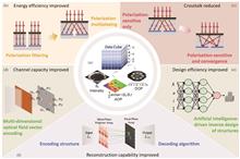
SignificanceInfrared polarization detection technology, beyond mere intensity detection, enables the extraction of the polarization characteristics of infrared radiation from targets. These characteristics reveal the material properties, surface morphology, and physicochemical traits of the target and its surroundings, making this technology essential for military, civilian, and medical applications. In particular, focal plane array-based infrared polarization detectors have garnered significant attention from researchers owing to their high level of integration and real-time imaging capabilities. However, as the pixel size of infrared focal plane arrays continues to shrink, approaching the scale of the characteristic wavelength, there is an increasing demand for efficient polarization decoupling at the pixel level using microstructures. Furthermore, polarization structures must be vertically integrated at the pixel level with the pixel arrays to ensure accurate and efficient transmission of polarization components to the absorption region. These requirements place stringent demands on the design and integration of polarization micro- and nano-structures.ProgressIt is a significant challenge for traditional imaging systems to capture the polarization information of a target’s light field, which typically requires bulky optical components and time-domain multiplexing. Conventional polarization-detection technologies, such as time-division, amplitude-division, and aperture-division schemes, suffer from drawbacks such as large size, system complexity, and low stability. In response to the demand for lightweight, highly integrated, stable, and real-time full-polarization infrared detection, pixel-level polarization-sensitive structures in infrared focal-plane array polarization detectors have become a key development direction for next-generation infrared detection technologies. Emerging technologies have driven significant advances in polarization filter devices with innovations such as metal wire grids, photonic crystals, and metasurfaces, enabled by nanofabrication technologies. These micro- and nano- structures, with immense potential for optical field manipulation, have become mainstream technologies in polarization detection devices. Currently, relatively mature polarization-integrated focal-plane arrays typically rely on subwavelength metal wire grids to achieve strong polarization sensitivity. These grids offer advantages such as high polarization selectivity, customizable broad operational bandwidth, miniaturization, high stability, and ease of integration. However, when the operational wavelength extends into the infrared range, the extinction ratio of the integrated polarization devices declines significantly compared to that of standalone wire grid arrays. Several researchers have analyzed the impact of key parameters such as pixel size, pixel pitch, distance between the polarizer and the photosensitive area, and alignment errors in integration on the polarization extinction ratio. All conclusions indicate that optical crosstalk between adjacent pixels becomes particularly severe in the infrared wavelength range, where the operational wavelength is comparable to the pixel size, resulting in diffraction effects that severely limit the extinction ratio of focal-plane infrared polarization devices.To address this issue, researchers have begun incorporating directional light field focusing into pixel-level micro and -nano-structures to reduce crosstalk between adjacent pixels. They are also advancing polarization multiplexing techniques to enhance energy utilization efficiency in weak-light infrared detection. These efforts are aimed at accelerating the practical applications of infrared polarization imaging devices. This paper reviews a series of notable works on polarization filtering/multiplexing and the implementation of pixel-level light field focusing (see Table 1), comparing key metrics such as operational wavelength range, energy utilization efficiency, number of polarization-encoded channels, unit cell size, and focal length. Given the impact of pixel-level discretized phase control and micro-nano fabrication errors, there is significant interest in ensuring the extinction ratio and other performance parameters of focal-plane array polarization detectors. New approaches, including the inverse design of novel microstructures, the integration of microstructures with pixel arrays, and the correction and reconstruction of readout signals, are being explored. These methods hold promise for driving efficient device optimization and achieving performance improvements beyond the limitations imposed by design and fabrication errors.Conclusions and ProspectsThis study reviews research progress on focal-plane array integrated infrared polarization detectors based on polarization-sensitive microstructures. It focuses on key issues such as improving energy utilization, reducing crosstalk between adjacent pixels, increasing the number of multiplexing channels, and enhancing structural design efficiency. This review discusses various design approaches and advancements in pixel-level polarization-sensitive microstructures. Additionally, from the perspective of integrated polarization devices, this study analyzes the key technologies related to polarization decoupling and reconstruction that affect polarization detection capabilities. The proposal and optimization of these design methods have facilitated a series of concept-level experimental validations of on-chip polarization imaging, thereby accelerating the development of application-grade integrated devices.Advancing the development of on-chip infrared polarization imaging devices based on micro- and nano-structures is of significant importance. Future research and applications should focus on several key innovations: AI-driven design of micropolarizers, designing pixel-level microstructures and key parameters of pixel arrays from an integrated device perspective, and establishing comprehensive polarization component transmission models for polarization calibration and reconstruction. By aligning with practical requirements and integrating multidisciplinary design approaches, this field offers new technological pathways for the development and application of miniature optical imaging systems in infrared polarization and spectroscopy.
Mar. 17, 2025Vol. 52 Issue 5 0501002 (2025)
Jing Lang, Fujun Xu, Jiaming Wang, Weikun Ge, and Bo Shen
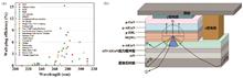
SignificanceAlGaN-based deep-ultraviolet light-emitting diodes (DUV-LEDs) are highly demanded in environmental monitoring, food safety, solar-blind communication, and detection. Owing to their competitive advantages such as low voltage, small size, long lifespan, and, more importantly, no mercury pollution, they are regarded as the preferred ultraviolet (UV) solid light source for replacing the conventional mercury lamp. However, the current performance of DUV-LEDs cannot satisfy the requirements of industrial applications, which is primarily due to their low light-extraction efficiency (LEE). Therefore, a comprehensive review of the research progress on LEE will enable readers to comprehensively understand the key problems and the corresponding strategies, thus facilitating the further development of AlGaN-based DUV-LEDs.ProgressAlGaN-based DUV-LEDs have been investigated since the early 21st century. Owing to significant efforts in the following decades, the highest wall-plug efficiency (WPE) of devices achieved is 15.3%, whereas that of commercial chips is lower than 6% (Fig. 1). The WPE is determined by the carrier injection efficiency (CIE), internal quantum efficiency (IQE), LEE, and device operating voltage, among which the LEE is the major bottleneck that limits the further enhancement of device performance. Three key scientific and technological issues result in low LEEs: optical polarization, optical total reflection, and optical absorption. Specifically, the active region with Al-rich AlGaN as quantum wells presents a low polarization degree, thus resulting in a large proportion of transverse magnetic (TM)-polarized light emission, which complicates light extraction from the bottom of substrates. Total reflection is resulted from the significant difference in the refractive index between adjacent materials at the interface, e.g., AlN/substrate or substrate/air. To achieve light absorption, thick p-GaN is the common choice for the capping layer, not only for hole supply but also for the formation of Ohmic contacts with conventional Ni/Au electrodes, as p-GaN can realize efficient doping more easily than p-AlGaN. However, GaN with a narrow bandgap does not allow DUV light to pass through. Consequently, the p-GaN capping layer, together with p-type electrodes, absorbs almost all the DUV light emitted upwards. Solutions to address the issues above can be summarized as follows.First, because TM-polarized light cannot be extracted easily, the polarization degree of the quantum wells can be improved via energy-band regulation (Fig. 2). Another strategy is to reduce the size of the active region and introduce a reflector at the sidewall during device fabrication (Fig. 3).Second, the issue of total reflection can be categorized into two types: reflection at the interface between the epilayers and that at the interface between the substrate and air. For the former, air voids are typically introduced to change the light-propagation path, thus allowing the limit of the total reflection angle to be exceeded (Fig. 4). For the latter, removing the substrate, roughening the substrate surface, or introducing encapsulation can increase the angle of the light-escape cone (Fig. 5).Third, optical absorption can be weakened by adopting a p-type region with high DUV transmittance and p-type electrodes with high reflectivity. Efficient doping in p-AlGaN is the key breakthrough in absorption by the epilayers; in this regard, superlattice and polarization-induced doping have been proven to be effective (Fig. 6). Additionally, composite electrodes may be more suitable for industrial applications, considering their cost (Fig. 7).Conclusions and ProspectsAlGaN-based DUV-LEDs are intensively investigated in studies pertaining to group-Ⅲ nitride semiconductors and optoelectronic devices. Owing to the current global prohibition of mercury lamps, the development of DUV-LEDs with high WPE and their further industrial application are highly demanded. Currently, light extraction is a key technical bottleneck restricting the improvement in device performance; thus, it is extensively investigated worldwide. This paper focuses on three factors contributing to low LEEs and reviews the relevant technical innovations in recent years. In terms of optical polarization, the active region at the microscale demonstrates significant potential for the extraction of TM-polarized light and is expected to become the main aspect for future device configurations. For optical reflection, weakening the total reflection at the interface between the substrate and air may be the most effective method. Developing methods to remove substrates nondestructively or preparing high-quality AlN single-crystal substrates requires greater effort. In terms of optical absorption, studies pertaining to transparent Al-rich p-AlGaN and p-type electrodes with high reflectivity should be conducted simultaneously. New optical phenomena, such as the oscillation and coupling of photons/electrons in micro-nano photonic structures, should be investigated further. In summary, the development of AlGaN-based DUV-LEDs has progressed rapidly in the past two decades. However, the LEE must be further enhanced to satisfy the demands of commercial applications, which entails the exploration of new routes and technologies.
Mar. 08, 2025Vol. 52 Issue 5 0501003 (2025)
Jiajian Chen, Zhiqiang Guo, Wenqi Wei, Ting Wang, Min Tan, and Jianjun Zhang
SignificanceWith the gradual waning of the Moore’s Law, the sustainable development of the semiconductor industry faces a significant challenges and opportunities. Integrating photonics into microelectronics is expected to provide new momentum for the sustainable development of the semiconductor industry. Electronics-photonics convergence combines the advantages of electronics in areas such as computation and storage with the advantages of photonics in areas such as transmission capacity and interference resistance. This convergence is expected to shape the shared future of both microelectronics and photonics.A light source is a prerequisite for implementing any electronic-photonic system. Traditional light sources are typically independently fabricated without special optimization for electronics-photonics convergence. As integration levels and performance metrics of electronic-photonic systems continue to rise, light source integration has become a bottleneck problem limiting the practical implementation of many applications. This paper reviews the development status of integrated light source technologies geared towards various applications in the context of electronics-photonics convergence, elucidates the associated challenges and their solutions, and further summarizes and anticipates future development directions of integrated light source technologies.ProgressOptical communication, as the most significant application field for integrated light sources, attracts most research interest and devotion. Here in this work, development in mainstream semiconductor lasers is included. The summary of integrated laser sources and corresponding modulation formats are listed in Table 1. Several important progresses are included: VCSEL transmission rates have advanced significantly. In 2024, Intel reached 64 Gb/s and 256 Gb/s in a four-channel setup. DFB lasers have also progressed in modulation rates. In 2021, Yamaoka achieved a 108 GHz bandwidth and a 256 Gb/s PAM-4 modulation rate. High transmission rates have also been achieved through external modulation techniques. Other lasers such as microring lasers, micro-LEDs, and semiconductor mode-locked lasers have also made progress. For example, in 2018, Liang Di demonstrated a mixed-integrated microring laser with a modulation rate of 14 Gb/s and a modulation bandwidth of 14.5 GHz (Fig. 2).In other application fields, such as frequency modulation continuous wave LiDAR and optical coherence tomography, significant efforts have been devoted to improving on-chip laser source performances. In 2024, Sanghonn Chin achieved an on-chip ECL with lateral resolution of 9 μm. A Ga/Sb gain chip is integrated with SOI PIC chip as laser source for FMCW LiDAR, tunability is based on the vernier effect of double micro-ring resonators. Broad band SLED and tunable ECL are also studied for OCT purposes, they aimed to achieve larger tunable range and tuning speed.Common challenges faced by on-chip lasers and corresponding solutions are also discussed. Narrow linewidth is an important factor for coherent communication laser sources as it directly affects signal quality. Tunable external cavity lasers with waveguide structures exhibit promising linewidth properties, but coupling issues remain a challenge. To address this, solutions such as anti-reflection coatings and evanescent wave coupling have been proposed to improve coupling efficiency, thereby enhancing performance in optical communication applications.Efficient coupling of light from on-chip lasers to waveguides is another key challenge, particularly due to mode spot mismatches and thermal effects. Techniques like grating couplers, which use diffraction, and adiabatic couplers, which rely on gradual changes in waveguide geometry, have been developed to minimize losses. Additionally, end-face direct coupling and light lead coupling, which involve the laser directly attaching to the waveguide or using guiding structures, respectively, have shown promise in ensuring efficient light transfer.Also, multi-wavelength lasers often have lower and non-uniform power compared to single-wavelength lasers. For mode-locked lasers, on-chip amplifiers can boost power. For Kerr-comb lasers, using pulse lasers for pumping improves energy conversion efficiency, resulting in a more powerful multi-wavelength source suitable for various applications.Lastly, To achieve high integration level between laser sources and on-chip photonics devices, direct heterogenous epitaxial growth is prompted as an effective method, where the III?V materials such as InP or InAs can be directly deposited on silicon substrates. Although there exist some challenges like lattice, polarity, and thermal mismatches. Buffer layers can reduce lattice mismatch, while specific substrate structures can minimize polarity and thermal mismatch effects. Optimizing growth techniques, such as temperature and pressure, can further enhance laser quality. These solutions are essential for developing integrated light sources for semiconductor devices.The review includes remarkable progress on silicon-based growth of III?V quantum dot lasers. In 2011, Wang et al. achieved pulsed lasing of InAs quantum dot lasers on a slanted Si substrate at a 1.3 μm wavelength. In 2015, Chen et al. achieved room-temperature continuous lasing of InAs quantum dot FP lasers on a slanted Si substrate with improved performance. Between 2018 and 2019, Jung and Shang et al. developed high-performance quantum dot lasers with enhanced characteristics. In 2018, Wei et al. addressed challenges related to lattice, polarity, and thermal mismatches, achieving a Si-based InAs quantum dot FP laser with good performance. In 2023, Wei et al. demonstrated the monolithic integration of on-chip III?V lasers and Si waveguides, achieving direct coupling with good performance (Fig. 8).Conclusions and ProspectsEmerging applications demand integrated light sources. While considerable progress has been made, further innovations in materials, processes, and techniques are required for practical use. These advancements will accelerate the adoption of electronics-photonics integrated chips and may lead to a new industrial cycle akin to Moore’s Law.In summary, although significant advancements have been achieved, continued efforts are necessary for the full realization and widespread use of integrated light sources, potentially ushering in a new era of semiconductor industry growth.
Mar. 17, 2025Vol. 52 Issue 5 0501004 (2025)
Bing Xiong, Mingwei Sun, Changzheng Sun, Zhibiao Hao, Jian Wang, Lai Wang, Yanjun Han, Hongtao Li, Lin Gan, and Yi Luo
SignificanceThe explosive growth in data traffic has driven the relentless pursuit of higher data transmission speeds and bandwidths. Photonic devices with ultrawide bandwidths are crucial for next-generation networks. Moreover, these ultrafast optoelectronic devices hold significant promise for the oncoming sixth-generation (6G) systems and millimeter-wave (MMW) / terahertz (THz) wireless communication systems.With electron-only transportation in the drift layer, uni-traveling carrier photodiodes (UTC-PDs) have significant potential for applications in optical communication, data interconnection, and microwave photonics owing to their exceptional characteristics such as wide bandwidth and high saturation. The bandwidth of photodiodes (PDs) directly limits the maximum data transfer rate. PDs with high responsivity not only alleviate tight fiber alignment tolerances but also enable extended link distances, reduce overall power consumption, and contribute to enhancements in the dynamic range and a higher signal-to-noise ratio (SNR). However, for surface-illuminated PDs, there is a tradeoff between bandwidth and responsivity. For waveguide PDs, the direction of light transmission is perpendicular to the direction of carrier transport, and high responsivity and wide bandwidth can be achieved simultaneously by decoupling the absorption efficiency and carrier transport.The bandwidths of the PDs are determined by the carrier transmission time and resistance capacitance (RC) time constant. Epitaxial structures should be optimized to take advantage of the electron overshoot effect, thereby reducing the electron transport time in the drift layer. To address the constant RC limitation, improvements can be made not only by optimizing the epitaxial structure but also by reducing the parasitic capacitance and lowering the contact resistivity. In addition, high-impedance lines can be used to compensate for the device capacitance, and parallel resistors can be added to decrease the overall resistance.ProgressThe development of chips and packaging technologies has been introduced. A carefully designed waveguide coupling structure can enhance quantum efficiency. Edge-illuminated detectors have the simplest waveguide structure, in which the absorber serves as the waveguide core. However, incident light is concentrated at the front end of the absorption region, which can easily lead to local saturation, making it challenging to improve the saturation output characteristics. Evanescently coupled waveguide photodiodes can achieve relatively uniform light distribution along the absorber, thus improving their high-power handling capability. To improve the coupling efficiency between the waveguide and the input fiber, PDs integrated with spot-size converters are typically adopted. Rouvalis et al. fabricated PDs integrating a horizontal taper. Demiguel et al. proposed evanescently coupled PDs integrating a double-stage taper with a bandwidth of 40 GHz and high responsivity of 0.6 A/W. Umbach et al. designed waveguide PDs with vertically tapered waveguides (Fig. 2). Campbell et al. proposed highly responsive evanescently coupled PDs integrating short planar multimode waveguides that are more compact, less complicated, and easily fabricated (Fig. 4). Our research group has proposed a thick multilayer waveguide with a gradually increasing refractive index as a coupling waveguide (Fig. 6).The bandwidths of the PDs are determined by the carrier transmission time and RC time constant. Epitaxial structures should be optimized to take advantage of the electron overshoot effect, thereby reducing the electron transport time in the drift layer. To address the constant RC limitation, improvements can be made not only by optimizing the epitaxial structure but also by reducing the parasitic capacitance and lowering the contact resistivity. In addition, high-impedance lines can be used to compensate for the device capacitance, and parallel resistors can be added to decrease the overall resistance. The performance of the waveguide PDs is summarized in Table 1.For practical use in these systems, UTC-PD chips must be packaged into modules. Three packaging forms of detectors—coaxial output, waveguide output, and antenna radiation—and their effects on the output electrical signal are introduced. The performance of the reported modules is summarized in Table 2.Conclusions and ProspectsThe continuous growth in data traffic requires high-speed detectors to match the required bandwidth. High-speed waveguide UTC-PDs can be utilized as receivers in high-data-rate optical communications. Additionally, they can serve as transmitters in MMW/THz wireless communications to deliver high-power and high-frequency microwave signals. Using waveguide optical coupling, multiple photonic devices can be integrated on a chip to create a high-density photonic integrated circuit.
Mar. 15, 2025Vol. 52 Issue 5 0501005 (2025)
Guangjie Yao, Jiacheng Li, Huazhan Liu, Chaojie Ma, Hao Hong, and Kaihui Liu
SignificanceLight carries information and energy simultaneously. Manipulating light for communication and energy conversion significantly promotes the progress of human society. Initially, different types of lenses and mirrors are used to help people view further and smaller through telescopes and microscopes. Phenomena such as reflection, refraction, interference, and diffraction are well studied. Among these, the polarization density (P) within a medium is proportional to the electric field (E) of excitation light. As light intensity increases (specifically when a high-power laser is invented and introduced to optical research and production), interactions between medium and intense light fields normally show results that are different from those under traditional conditions. The concepts and applications of nonlinear optics are currently at the optical research stage.Nonlinear optics, which describes the nonlinear interactions between light and nonlinear medium (i.e., P depends nonlinearly on E), is a significant component of modern optics for both fundamental research and technical applications. Nonlinear interactions involve various processes such as harmonic generation, spontaneous parametric downconversion, the Kerr effect, and the electro-optic effect. Utilizing these processes, we can expand the usable laser wavelength range from deep ultraviolet to terahertz bands and create light sources carrying quantum information. Various types of instruments based on nonlinear optics are available in optical laboratories and factories. Mode-locked lasers produce ultrashort laser pulses for time-resolved measurements and laser manufacturing. Optical parametric oscillators and optical parametric amplifiers can be used to produce wavelength-tunable lasers. Quantum light sources create entangled photon pairs for quantum communication. In these applications, the core components are efficient nonlinear processes. However, weak nonlinear interactions between most medium and phase mismatches result in low conversion efficiency. There are two main ways to improve the overall efficiency: finding materials with high nonlinear coefficients and exploring a highly efficient corresponding phase matching method.Various high-performance optical crystal materials, including organic and inorganic materials, are studied and are still being widely pursued. Simultaneously, suitable phase matching methods are required for high conversion efficiency, which is crucial for practical applications. Phase matching methods are typically developed for a series of optical crystal materials with common properties. For example, birefringent phase matching is used for crystals with strong birefringent properties, whereas quasi-phase matching is suitable for polarized crystals. Therefore, the search for new types of high-performance nonlinear optical crystals must be accompanied by the corresponding phase matching methods. With the emergence of diverse materials with different properties, optical crystal material families and phase matching methods are being replenished.ProgressDifferent types of nonlinear crystals and their corresponding phase matching methods have been developed over the past few decades. The most commonly used phase matching method is birefringent phase matching, which is first proposed in 1962. Here, a birefringent crystal separates the fundamental wave and second-harmonic generation (SHG) wave along different optical axes. A carefully selected incident polarization angle and cut angle of the crystal are required for precise refractive-index matching between the fundamental wave and SHG wave (Fig. 3). Utilizing birefringent phase matching, deep-ultraviolet laser generation is achieved with high conversion efficiency. Next, quasi-phase matching with inversion-poled domains is studied based on polarized materials such as lithium niobate crystals. The wavevector mismatch between the fundamental wave and the SHG wave is filled by a predesigned superlattice (Fig. 5). Through a unique periodic structure design, phase matching for third- and higher-order harmonic generation is realized, demonstrating the flexibility of quasi-phase matching (Fig. 6). Two-dimensional optical crystal materials attract significant attention because of their high nonlinear coefficients and excellent integration abilities (Fig. 7). However, traditional phase matching methods, such as birefringent and quasi-phase matching, cannot be applied to two-dimensional materials directly. The newly developed twist phase matching method can be used on layered materials, which exhibits high conversion efficiency and flexibility for two-dimensional materials such as rhombohedral boron nitride and one-dimensional materials such as multiwalled boron nitride nanotubes (Fig. 8).Conclusions and ProspectsIn conclusion, different types of nonlinear optical crystals and their corresponding phase matching methods are developed for various applications. Nowadays, new families of optical crystals are under study for higher conversion efficiencies, broader wavelength ranges, and novel functionalities. New phase matching mechanisms for highly efficient and universally applicable nonlinear crystal materials are also being pursued. In the future, optical crystals together with corresponding phase matching methods working in the extreme wavelength range (i.e., deeper ultraviolet and longer terahertz wavebands), generating ultrahigh output power, integrating with on-chip photonic circuits, and carrying quantum information are predicted to remain in high demand.
Mar. 07, 2025Vol. 52 Issue 5 0501006 (2025)
Guangzhou Cui, Yongqiang Sun, Kai Guo, Jinchuan Zhang, Fengqi Liu, and Shenqiang Zhai
ObjectiveQuantum cascade lasers (QCLs) are a type of unipolar light source based on electronic transitions between sub-bands in semiconductor-coupled quantum wells and phonon-resonant tunneling. Their small size, high power, and wide tunability render them highly versatile, with broad applications in biosensing, infrared spectroscopy, gas detection, and free-space communication. Currently, owing to its precise control over the material composition as well as its epitaxial layer thickness and sharp heterointerfaces, molecular beam epitaxy (MBE) serves as a critical technique for fabricating high-quality QCLs. However, limitations in production capacity and extended maintenance periods render MBE inadequate for meeting industrial demands. In this study, we report the successful growth of lattice-matched QCL material utilizing metal-organic chemical vapor deposition (MOCVD) on highly doped InP substrate, targeting an emission wavelength of 10.13 μm. The favorable performance of the device validates the potential of MOCVD for the epitaxial growth of long-wavelength infrared QCLs.Mechods As the excitation wavelength and doping concentration both increase, the waveguide loss also increases, resulting in a higher threshold current density and deteriorated device performance. When the doping concentration in the active region is rationally adjusted and the doping of the waveguide layer is optimized, the waveguide loss can be reduced and materials with superior heterointerface quality can be grown. In this study, the optimized structure of a QCL was grown on a 2-inch InP substrate (Si doping concentration of 2×1018 cm-3) using MOCVD at 100 mbar. The group III precursors were trimethyl indium (TMIn), trimethyl gallium (TMGa), and trimethyl aluminum (TMAl), and the group V precursors were arsine (AsH3) and phosphine (PH3). Silane (SiH4, volume fraction of 0.02%) was employed as the N-type dopant, with the growth temperature maintained between 630 and 660 ℃. The growth structure consisted of the following sequential layers: a 500-nm InP buffer layer (Si doping concentration of 1×1017 cm-3), 3-μm InP lower waveguide layer (Si doping concentration of 2×1016 cm-3), 50-period lattice-matched active region, 3-μm InP upper waveguide layer (Si doping concentration of 2×1016 cm-3), 0.5-μm grade-doped InP layer (Si doping concentration from 2×10¹⁶ to 5×1017 cm-3), and 0.5-μm high-doped InP cap layer (Si doping concentration of 2×1018 cm-3). The QCL core was fabricated into a ridge waveguide structure with an average ridge width of 15.2 μm using a semi-insulating InP buried heterostructure process (Fig. 2). This structure was then partitioned into devices with a cavity length of 4 mm, with a high-reflectivity (HR) coating applied to the rear facet and the front cavity facet left uncoated. The devices were epi-down on diamond submounts and subsequently mounted on copper heat sinks with indium-coated surfaces to enhance thermal dissipation.Results and DiscussionsHigh-reflection X-ray diffraction (HRXRD) measurements reveal a strong correspondence between the experimental data and theoretical simulations of the satellite peaks. The presence of sharp, well-defined, high-order satellite peaks with a narrow full width at half maximum (FWHM, 12 arcsec) underscores the uniformity of the chemical composition in the cascade structure and the quality of the heterointerfaces (Fig.1). The maximum peak output power achieves 0.96 W at 293 K, with a slope efficiency of 1.14 W/A and threshold current density of 0.68 kA/cm2 in pulsed mode. For continuous wave operation, the highest output power is 0.52 W, with a peak current of 1.15 A, slope efficiency of 1.0 W/A, and threshold voltage of 9.5 V at 293 K, whereas the maximum wall plug efficiency (WPE) reaches 4% (Fig.3). A longer cavity length reduces the mirror loss, and lower doping concentrations in the waveguide layer and active region mitigate the free carrier absorption loss, thereby decreasing the overall absorption loss. In addition, the device grown by MOCVD exhibits a narrow FWHM in the HRXRD measurements, indicating superior quality at the heterointerfaces. This enhanced quality contributes to reducing interface roughness scattering, improving the excited-state electron lifetimes, and effectively suppressing nonradiative loss. Collectively, these factors result in a decrease in the threshold current density and an increase in the output power and WPE. The emitted laser spectrum has a center wavelength at 986.9 cm-1 (10.13 μm) at an input current of 0.6 A in continuous wave mode. The beam image confirms that the device operates in transverse mode (TM00), see Fig.4. Fitting the temperature dependence of the threshold current density and slope efficiency in the pulsed mode enables the characteristic temperatures of the threshold current density (T0) and slope efficiency (T1) to be determined as 156 K and 301 K, respectively (Fig. 5). Due to non-harmonic oscillators, a wider FWHM of the electroluminescence (EL) spectrum typically contributes to increasing interband loss, which in turn decreases the peak gain and increases the laser threshold current density. In our experiments, the narrow EL FWHM of 114.7 cm-1 (17.2 meV) aligns with the previously recorded low threshold current density (Fig. 6).ConclusionsThis study reports a long-wavelength infrared QCL with a full structure grown using MOCVD. By optimizing the doping concentrations in the waveguide layers, we effectively reduce the waveguide loss and develop an active-region structure with high-quality heterointerfaces. The laser with a cavity length and ridge width of 4 mm and 15.2 μm, respectively, achieves a continuous wave output power of 0.52 W at room temperature. This is accompanied by a remarkably low threshold current density of 0.76 kA/cm2 and maximum WPE of 4%. In the pulsed mode, a peak output power of 0.96 W is obtained, and the characteristic temperatures for the threshold current density and slope efficiency are 156 K and 301 K, respectively. The lasing wavelength is measured at 10.13 μm, with a clear TM00 mode observed. The excellent performance of this device demonstrates the potential of MOCVD for epitaxial growth of long-wavelength infrared QCLs.
Mar. 07, 2025Vol. 52 Issue 5 0501007 (2025)
He Hao, Gaoda Ye, Suheng Li, Ran Ding, and Jing Feng
SignificanceAs one of the most important inventions in the 20th century, the laser has been widely termed “the fastest knife,” “the most accurate ruler,” and “the brightest light.” A laser represents light amplification by the stimulated emission of radiation, which can explain the lasing generation process. Organic lasers, as important components of lasers, have received extensive attention in the field of optoelectronics for various applications owing to their advantages, such as facile fabrication, low cost, and ease of integration. Recently, organic lasers have been used extensively, and the design and synthesis of a series of promising organic-laser gain media have intensified. The development of optically pumped organic lasers has progressed significantly; however, the aim of electrically pumped organic lasers remains a worldwide research problem. Owing to the three key components of organic lasers, the fabrication of optical resonators is crucial to realize efficient and stable electrically pumped organic lasers.ProgressHere, we summarize the recent novel developments of electrically pumped organic lasers, from material selection to device optimization. Three types of optical resonators are typically used in electrically pumped organic lasers: distributed feedback structures (DFBs), distributed Bragg reflectors (DBRs), and whispering gallery mode (WGM). To realize electrically pumped organic lasers, the following criteria must be satisfied: sufficient current injection and exciton densities to induce population inversion, clear threshold behavior of current-density-dependent spectral narrowing and output-power enhancement, and observation of both spatial and temporal coherence. Figure 1 shows the organic four-level system under electrical excitation and the lasing behavior of the output power and FWHM (full width at halt maxima) as a function of current density. In Section 2.1, we summarize the recent developments of electrically pumped organic lasers based on DFB resonators. DFB resonators are considered to be among the most effective structures for realizing electrically pumped organic lasers. They are essentially periodic Bragg-grating structures that can provide effective optical feedback for lasing oscillations via Bragg scattering. Figure 2 illustrates an electrically pumped organic laser with a DFB structure, in which an electroluminescent device incorporates a mixed-order distributed feedback SiO2 grating into an organic light-emitting diode (OLED) structure and emits blue lasing. Figure 3 shows an electrically driven organic laser with an integrated device structure that efficiently couples an OLED with exceptionally high internal-light generation and a polymer-distributed feedback laser. Under electrical driving, a threshold in the light output versus the drive current with a narrow emission spectrum and the formation of a beam above the threshold are observed. Section 2.2 summarizes the recent novel developments of electrically pumped organic lasers based on DBR resonators. DBR resonators are periodic structures comprising alternating layers with different refractive indices, where the optical thickness of each layer corresponds to a quarter of the reflected wavelength. Owing to their vertical structure, DBR resonators can be integrated well with OLEDs. Additionally, they can effectively confine light to the cavity by reflecting it, thereby realizing laser oscillation. Figure 4 shows a DBR microcavity organic laser that observes electrically pumped quasi-continuous-wave lasing at an extremely low current density. Polariton lasing originates from the leakage of coherent photons from macroscopic exciton-polariton (EP) condensates via stimulated scattering, which is also known as the Bose?Einstein condensation (BEC) of EPs. Because population inversion is no longer required, polariton lasers are considered an alternative that may facilitate the development of practical electrically pumped organic lasers with much lower thresholds. As shown in Figure 5, strong coupling between excitons and cavity photons, referred to as room-temperature polariton lasing, is successfully observed in planar DBR cavities containing two new fluorene-based oligomers, BSFCz and BSTFCz. Within the WGM resonators, light is trapped owing to the total internal reflection at the interface, thereby realizing lasing oscillation. Section 2.3 summarizes the recent novel developments of electrically pumped organic lasers based on WGM resonators. WGM resonators typically possess high quality factors; however, their small size renders their fabrication and integration difficult. Figure 6 shows the realization of large microdisk arrays based on organic single crystals with the observation of WGM lasing from these microresonators.Conclusions and ProspectsThis study focuses on electrically pumped organic lasers. Based on different optical resonators, we summarize the recent novel developments of electrically pumped organic lasers from material selection to device optimization and then discuss the future development trends of electrically pumped organic lasers. Recent efforts toward electrically pumped organic lasers are important in the roadmap of organic lasers, which not only help us clarify the role of material synthesis, resonator design, device optimization, and photophysics in electrically pumped lasing but also provide insights into the fundamental knowledge, technologies, and strategies for solving the worldwide research problem of electrically pumped organic lasers.
Mar. 07, 2025Vol. 52 Issue 5 0501008 (2025)
Yufei Hou, Jing Yang, and Degang Zhao
ObjectiveAlGaN/GaN multiple quantum wells (MQWs), as the core light-emitting regions of optoelectronic devices such as ultraviolet light-emitting diodes (LEDs) and laser diodes (LDs), greatly impact the performance of such devices. However, due to the large lattice mismatch between the AlGaN material and the substrate, a large number of defects exist in AlGaN/GaN MQWs, which seriously affects the luminescence characteristics of the MQWs. In addition, polarization, quantum confinement Stark effect, and localized state effect can also impact the luminescence efficiency of MQWs; in particular, the localized effect has a significant influence on the luminescence uniformity of ultraviolet MQWs. Therefore, study of the factors affecting the luminescence of AlGaN/GaN UV MQWs will contribute to a better understanding of the luminescence mechanism of MQWs, and leads to high-performance GaN-based ultraviolet optoelectronic devices.MethodsIn this work, three samples of AlGaN/GaN MQWs are grown on sapphire substrates using metal-organic chemical vapor deposition (MOCVD). First, the components and thicknesses of the samples are determined via X-ray diffractometer (XRD). Their room-temperature photoluminescence (PL) spectra are then obtained using a PL system with a 325 nm He-Cd laser as the excitation source. Finally, the luminescence mechanism of the sample is analyzed via temperature dependent PL spectroscopy.Results and DiscussionsFrom the room-temperature PL spectra, the luminescence intensity of the quantum well first increases and then decreases as the well width increases (Fig. 1). In addition, temperature dependent photoluminescence spectroscopy tests indicate that as the temperature increases, the emission wavelength of the ultraviolet quantum well first shifts blue and then red; this phenomenon is more apparent for the samples with wider wells (Figs. 2 and 3). Furthermore, the luminescence of the ultraviolet quantum well exhibits localized state effects similar to those from blue-green light quantum wells, which becomes more significant as the well width increases. This may be due to the fact that the polarization properties, fluctuations in well width, and inhomogeneity of the Al composition of the barrier layer together lead to varying quantum confinement effects in the well layer.ConclusionsThree AlGaN/GaN ultraviolet MQW samples with different well widths are epitaxially grown on sapphire substrates using MOCVD, and their luminescence characteristics are investigated. As a result, excessively narrow well layers can lead to a decrease in PL intensity and a blue shift in the MQW peak, while increasing the quantum well width appropriately is beneficial for improving PL luminescence intensity. This phenomenon may be due to polarization characteristics, fluctuations in well width, and uneven Al composition in the barrier layer. Moreover, wide wells have different quantum confinement effects, resulting in localized state effects similar to those from blue-green light quantum wells, thereby enhancing ultraviolet luminescence intensity.
Mar. 15, 2025Vol. 52 Issue 5 0501009 (2025)
Jianxin Tang, Ni Xiong, Xinyu Cao, and Yang Shen
SignificanceIn recent years, perovskite materials have been employed in the fabrication of light-emitting diodes (LEDs) because of their adjustable bandgaps, long carrier diffusion lengths, high exciton binding energies, and high fluorescence quantum yields. Hence, they exhibit considerable potential for use in display and lighting applications. In 2014, Tan et al. developed a perovskite light-emitting diode (PeLED) that emits light at room temperature employing a class of metal halide perovskites (MHPs). In subsequent studies, scientists have conducted extensive research on perovskite crystal quality and device structure, resulting in rapid advancements in PeLED technology, particularly with regard to the enhancement of electroluminescence performance.Although the performance of PeLEDs has approached or even surpassed that of other commercial LEDs, numerous challenges inherent to the production and application of these devices remain unaddressed. PeLEDs exhibit poor stability and the manufacturing process is constrained by the difficulty involved in fabricating large-area devices, environmental pollution caused by lead, and leakage of organic solvents. Device stability is the most significant in these challenges and constitutes a noteworthy impediment to the commercialization of PeLED technology. Additionally, the operational lifetimes of PeLEDs are still shorter than those of mature organic and quantum dot light-emitting diodes by 2?3 orders of magnitude. The poor stability of PeLEDs can be attributed to the variety of defects inherent to perovskite materials. The most notable characteristics are deep-level defects, which can be considered the primary factors influencing device stability. Furthermore, the interfacial charge accumulation, ion migration, and Joule heat generated during the operation of a PeLED device, as well as the sensitivity of the devices to environmental factors (humidity, light, and temperature) caused by defects accelerate interfacial degradation, resulting in device damage. Although PeLED technology continues to evolve, its commercialization will inevitably be hindered by these stability issues.ProgressThis review briefly discusses the evaluation criteria for device stability and analyzes their advantages and disadvantages. In addition, the main factors influencing PeLED stability are identified (Fig. 1). Subsequently, different optimization strategies for film passivation and device preparation are introduced and discussed, and effective schemes are summarized. Finally, this study outlines the issues that require immediate attention and proposes potential solutions to address these issues.Conclusions and ProspectsThis study summarizes the recent cutting-edge developments in the research on PeLED stability, summarizes the main factors affecting PeLED stability from the two perspectives of perovskite materials and LED devices, and discusses an optimization scheme based on these factors. The optimization strategy involved in this study includes the following three general objectives: film quality improvement, device structure optimization, and device thermal management. It is predicted that once the impediment of poor working stability is addressed in PeLED devices, the technology will evolve to produce a new generation of display and lighting devices with high efficiency, high color accuracy, high brightness, and low cost.
Mar. 08, 2025Vol. 52 Issue 5 0501010 (2025)
Lei Shi, Tao Yang, Yachao Wang, Lilong Ma, Leiying Ying, Yang Mei, and Baoping Zhang
SignificanceGallium nitride (GaN)-based vertical cavity surface-emitting lasers (VCSELs) exhibit luminescence wavelengths that span the entire visible spectrum. They present several advantages, including a reduced threshold current, narrower divergence angle, single longitudinal mode operation, and a circularly symmetric output beam. GaN-based VCSELs have the potential to supersede conventional light-emitting diodes (LEDs) and edge-emitting lasers (EELs) as optimal light sources for applications such as semiconductor laser illumination, laser displays, high-density optical storage, optical interconnects, and underwater communications. Over the past two decades, significant advancements in technology have positioned they as a focal point of research for next-generation semiconductor lasers.ProgressThe resonant cavity structures of GaN-based VCSELs are primarily classified into two types: hybrid distributed Bragg reflector (DBR) and dual-dielectric film DBR structures. In the hybrid DBR configuration, the upper reflector comprises a dielectric-film DBR, whereas the lower reflector consists of a nitride DBR. In contrast, the dual-dielectric-film DBR structure utilizes dielectric-film DBRs for both the upper and lower reflectors. Despite the significant advancements in the prevalent DBR configurations of GaN-based VCSELs, several technical challenges persist. For instance, the hybrid DBR structure faces issues such as complex epitaxial growth of the nitride DBR, extended growth durations, and high costs. Conversely, the dual-dielectric film DBR structure encounters issues such as elaborate fabrication processes, suboptimal quality of heteroepitaxial crystals, insufficient uniformity of cavity length, and challenges in mass production. To address these challenges, Hmaguchi et al. (2018) introduced an innovative GaN-based VCSEL featuring a curved mirror, marking the first instance of room-temperature pulsed lasing with electrically injected curved-mirror GaN-based VCSELs. This design mitigates the need for the demanding and expensive nitride DBR epitaxial growth process prevalent in hybrid DBR structures. Additionally, curved-mirror GaN-based VCSELs eliminate the complex substrate transfer process associated with dual-dielectric film DBR structures, facilitating homoepitaxial growth on GaN single-crystal substrates. This advancement yields high-quality active regions, which are crucial for high-performance laser devices. The planar-concave stable cavity structure of the curved mirror GaN-based VCSELs demonstrates extremely low diffraction loss, accommodating an extended cavity length (20?50 μm). This characteristic not only simplifies GaN substrate polishing and thinning, but also significantly enhances the thermal performance of the devices. The advantages of the curved-mirror structure suggest a promising trajectory for the commercialization of GaN-based VCSELs. In 2019, the same research group achieved the inaugural room-temperature continuous lasing of a GaN-based VCSEL with a curved DBR structure, achieving a threshold current of only 0.25 mA. Concurrently, Nakajima et al. increased the output power to 7.1 mW by optimizing the curvature radius of the curved DBR. In 2020, Hamaguchi et al. demonstrated room-temperature continuous lasing of a green VCSEL with a curved mirror on semi-polar GaN substrates and pioneered preliminary white-light display systems using blue and green VCSELs with curved mirrors, alongside GaAs-based red VCSELs. In 2023, Ito et al. further enhanced the wall-plug efficiency (WPE) of a curved GaN-based VCSEL to 13.4% while maintaining consistent performance across all devices in the VCSEL array. Palmquist et al. achieved continuous room-temperature lasing of a GaN-based VCSEL with a curved DBR structure incorporating a top-surface lens, thus eliminating the need for a curved mirror support process. The following year, they fabricated an m-plane GaN-based VCSEL with a SiO2 curved top lens, achieving a maximum side-mode suppression ratio of 30 dB.Conclusions and ProspectsThe GaN-based VCSEL with a curved-mirror structure, while exhibiting commendable attributes such as high stability, uniformity, low threshold, and substantial output power, is nonetheless confronted with several technical challenges: 1) the extended cavity length of the device, which results in a very narrow longitudinal mode spacing, complicates the attainment of single longitudinal mode operation and induces mode hopping in the emission spectrum with variations in injection current; 2) the substrate employed for the epitaxial growth of the device is Si-doped GaN, where the optical absorption loss is directly proportional to the doping level. Consequently, precise control of the doping level in the GaN substrate is essential for minimizing internal losses within the resonator cavity; 3) the high mechanical hardness and pronounced chemical inertness of GaN crystals render conventional chemical-mechanical polishing techniques challenging. Consequently, achieving the required substrate thickness without inflicting damage remains a significant processing challenge ; 4) despite the robust lateral optical confinement provided by the curved-mirror structure, the laser divergence angle tends to be large due to the extended cavity length. Notwithstanding these technical challenges, the development of curved-mirror GaN-based VCSELs is promising. Addressing these issues is expected to facilitate the eventual commercialization of GaN-based VCSELs.
Mar. 08, 2025Vol. 52 Issue 5 0501011 (2025)
Yihang Chen, Cheng’ao Yang, Tianfang Wang, Hongguang Yu, Jianmei Shi, Juntian Cao, Haoran Wen, Zhiyuan Wang, Zhengqi Geng, Yu Zhang, Donghai Wu, Yingqiang Xu, Haiqiao Ni, and Zhichuan Niu
SignificanceThe rapid advancement of micro-nano processing technologies has led to the development of highly integrated and reliable photonic chips, which in turn has enabled the development of miniature portable chemical and biological sensors. These sensors are increasingly utilized in applications such as human health monitoring and environmental assessment. Photonic chips incorporate various elements, including light sources, waveguides, gratings, resonant cavities, and detectors. However, the single silicon material cannot fulfill the requirements for all optical components. The indirect bandgap nature of silicon restricts its radiation efficiency, creating an urgent need for highly efficient integrated light-source solutions.Semiconductor lasers are lightweight, efficient, and reliable, making them well-suited for applications in solid and fiber laser pumping, optical communication, material processing, and molecular spectroscopy. They are ideal light sources for photonic chips. The operating wavelength of a semiconductor laser is closely linked to the energy band structure of the luminescent material. By leveraging various semiconductor material systems and employing energy band engineering, we can achieve a wide range of operating wavelengths across the electromagnetic spectrum . Currently, semiconductor lasers utilizing the direct recombination transition mechanism in material systems such as GaN, GaAs, and InP can achieve coverage of the electromagnetic spectrum from ultraviolet to near-infrared. After the adoption of quantum cascade design, the operating wavelength of lasers is no longer restricted by the material bandgap width, allowing operation in the far-infrared or even terahertz ranges. However, designing lasers that operate in the 2?4 μm wavelength range, corresponding to transition energies of 0.31?0.62 eV, pose significant challenges for both direct recombination and intersubband transitions in the aforementioned material systems. This wavelength range includes the characteristic absorption peaks for several molecules, including CH4, CO, CO2, C2H6, and HCl, and can be applied to areas such as blood glucose monitoring, making these operating wavelengths essential for photonic sensing chips. The antimonide material system, composed of GaSb, AlSb, InAs, and derived multi-component compound materials, effectively addresses the semiconductor light source gap in the 2?4 μm wavelength band. With comparable lattice constants, this material system features a bandgap in the range of 0.41?1.70 eV and can form type-I, -II, and -III heterojunctions, thus offering high flexibility in energy band design. Constructing type-I and type-II quantum wells enables highly efficient operation within the 2?4 μm band range.This study focuses on the foundational research related to mid-infrared antimonide light source photonic integrated chips. It begins with a discussion on the epitaxial growth of antimonide high-efficiency gain materials and the mode control of discrete single-mode antimonide devices. Building on this foundation, the study then presents the latest advancements in antimonide heterogeneous integration.ProgressThe study first discusses enhancements in radiation efficiency and the expansion of the wavelength range in antimonide lasers grown via GaSb-based epitaxy. Key developmental milestones are outlined in Tables 1 and 2. Significant contributions include the implementation of strained quantum wells, sophisticated waveguide designs that optimize internal losses and light field distribution, the incorporation of high In-component and quinary alloy barriers, and the introduction of type-I quantum well cascade lasers. The study then covers advancements in single-mode antimonide lasers. Addressing the oxidizable nature of the antimonide material system, various strategies, including metal grating laterally coupled distributed feedback (LC-DFB), etched dielectric grating laterally coupled DFB, and socketed ridge-waveguide lasers, are employed to achieve on-chip single-mode antimonide lasers exhibiting a high side-mode suppression ratio (Fig. 12). Finally, the study discusses progress in the silicon-based heterogeneous epitaxy of antimonide lasers. The adoption of techniques such as nucleation layers, miscut substrates, substrate surface reconstruction, and patterned substrates (Fig. 16) helps to solve the problems of lattice mismatch and antiphase domains. In parallel, innovations in in-plane electrodes and etched cavity surface techniques are developed to facilitate the fabrication of high-performance silicon-based antimonide lasers.Conclusions and ProspectsAntimonide lasers are important mid-infrared coherent light sources that offer the advantages of compact size, high efficiency, long lifespan, low cost, and straightforward integration. They play a crucial role in various applications such as spectroscopy, precision measurement, space communication, material processing, laser surgery, and laser pumping, thus covering a wide range of industrial, biomedical, and information and communication scenarios, and have scientific research and economic value. The progress achieved in power enhancement, wavelength expansion, longitudinal mode management, and heteroepitaxial integration of antimonide type-I quantum well lasers is promising. It is anticipated that miniaturized practical devices using high-performance antimonide mid-infrared light sources and silicon-based photonics will be realized in the near future.
Mar. 08, 2025Vol. 52 Issue 5 0501012 (2025)
Jianan Duan, Zhiyong Jin, and Luochen Qu
SignificanceQuantum dot lasers (QDLs) have emerged as a revolutionary technology for silicon photonics, addressing key challenges in integrating light sources into optoelectronic chips. QDLs exhibit excellent temperature insensitivity and defect tolerance, which significantly reduces the complexity of their fabrication. Unlike quantum well lasers, QDLs are less sensitive to temperature variations, which enhances their stability under uncooled conditions. Furthermore, their three-dimensional quantum confinement renders them less susceptible to defects arising from lattice mismatches during epitaxial growth, resulting in less performance degradation. This defect insensitivity simplifies the fabrication process, particularly for large-scale integration on silicon, and reduces the manufacturing challenges associated with dislocation defects. One of the most distinctive features of QDLs is their resistance to optical feedback, which is a critical attribute for the development of isolator-free silicon photonic integrated circuits. Conventional lasers suffer from performance degradation and operational instability when exposed to optical feedback and require bulky and expensive optical isolators. In contrast, QDLs maintain a stable performance even under strong feedback conditions, enabling more efficient chip designs and reducing manufacturing costs. This makes QDLs ideal for compact, efficient, and cost-effective on-chip light sources, which are in increasing demand to support high-performance technologies, such as next-generation communication, artificial intelligence, and cloud computing. Beyond feedback resistance, QDLs exhibit excellent four-wave mixing (FWM) efficiency, which is a key factor in dense wavelength division multiplexing (DWDM) systems. Efficient wavelength conversion is critical for maximizing the data transmission capacity, and QDLs surpass other laser technologies by enabling direct FWM in the light source, significantly enhancing the scalability and efficiency of integrated photonic systems. Moreover, QDLs are essential in mode-locked configurations to generate optical frequency combs, which are crucial for on-chip optical interconnects. These combs provide the stable, low-noise, broadband light sources necessary for high-capacity data transmission, making QDLs a key technology for future optical interconnects, particularly in data centers and high-performance computing environments.Progress QDLs have achieved significant advancements in three key areasoptical feedback insensitivity, FWM, and mode locking. A major breakthrough is their ability to maintain stable operation under strong optical feedback, which typically causes instability in traditional lasers. Studies show that QDLs can remain stable even under feedback levels as high as -7.4 dB without exhibiting chaotic behavior (Fig. 2). This level of insensitivity eliminates the need for bulky and expensive optical isolators, thus reducing the system complexity and costs, making QDLs an ideal choice for isolator-free silicon photonic circuits. In high-speed data transmission, QDLs have demonstrated impressive performance, achieving modulation rates of up to 25 Gbit/s over 2 km without performance degradation even in the presence of feedback (Fig. 3), positioning them as crucial components in short-distance high-speed optical communication systems.Another area of significant progress is the FWM capability of QDLs. FWM is a nonlinear optical process critical for DWDM systems that enables efficient wavelength conversion to maximize data transmission capacity. Owing to their broader gain spectrum and faster carrier dynamics, QDLs exhibit a much higher FWM conversion efficiency than that of quantum well lasers. P-doped QDLs, in particular, have demonstrated FWM efficiencies as high as -4 dB (Fig. 4), substantially enhancing the performance of DWDM systems by enabling more efficient on-chip wavelength routing. The direct integration of FWM-based wavelength converters onto silicon chips represents a significant advancement in silicon photonics, reducing power consumption and maximizing efficiency.QDLs also excel in mode-locked configurations, which are crucial for generating optical frequency combs, a series of evenly spaced frequency components essential for high-capacity data transmission, precise metrology, and spectroscopy. Mode-locked QDLs have successfully generated optical frequency combs with bandwidths exceeding 36 nm, which can be further expanded by combining multiple sources (Fig. 5). These lasers exhibit high coherence and low relative intensity noise, making them suitable for a wide range of applications including on-chip optical interconnects and coherent optical communication systems. The ability to generate high-quality low-noise frequency combs with a broad bandwidth establishes QDLs as key drivers of next-generation optical networks.Conclusions and ProspectsIn summary, QDLs are expected to become a foundational technology in silicon photonics, addressing critical challenges in the integration of photonic and electronic devices. Their unique properties, including low noise, high thermal stability, resistance to optical feedback, and efficient nonlinear optical processes such as FWM and mode-locked frequency comb generation, make them essential for future high-performance photonic integrated circuits. Ongoing research promises to further enhance their performances, paving the way for broader applications in isolator-free optical communication systems, quantum computing, and advanced sensing technologies. In addition to their technical advantages, QDLs offer scalability for on-chip systems, thereby presenting the potential for cost-effective mass production. As these lasers continue to evolve, they are expected to drive innovation not only in telecommunications and data centers but also in fields such as quantum cryptography, coherent communication, and precision metrology. Their role in next-generation photonic networks is critical for satisfying the growing demand for faster, more efficient, and secure optical communication technologies.
Mar. 17, 2025Vol. 52 Issue 5 0501013 (2025)
Chao Zhong, Hailong Hu, Tailiang Guo, and Fushan Li
SignificanceDisplay is a ubiquitous medium for visual-information transmission and interaction. Owing to the rapid development of the information age and the continuous improvement of living standards, display technology is being constantly developed to satisfy the requirements for high-quality image display. The rapid progress of artificial intelligence in recent years has resulted in increasingly intelligent display technologies that can adapt to different scenarios while constantly enhancing people’s visual experience and realizing human-computer interaction. The introduction of virtual/augmented reality (VR/AR) and other technologies has posed new challenges to display resolution and brightness. The current mainstream light-emitting diodes (LEDs) and liquid-crystal displays (LCDs) can no longer fulfill these requirements; hence, microdisplay technology must be further developed urgently to satisfy the requirements of display development. The current microdisplay technology is dominated by micro-light-emitting diodes (Micro-LEDs) and silicon-based drive organic electroluminescent diodes (Micro-OLEDs). However, the size effect of Micro-LEDs and the sidewall effect caused by their miniature size limit their light-emitting efficiency. Furthermore, they must be transferred in large quantities and their processing is demanding. Micro-OLEDs are limited by their ultrafine mask plate as well as precise positioning evaporation and harsh conditions, thus significantly limiting their cost.Quantum dots, as a nanoscale semiconductor light-emitting material used in display technology, offer many unique advantages, such as adjustable bandgap, high quantum yield, high color purity, and low power consumption. Quantum-dot light-emitting diodes (QLEDs) are a novel type of quantum-dot-based optoelectronic device introduced in the 1990s. After their development for almost 30 years, their luminescence has improved significantly, and their current external quantum efficiencies of red, green, and blue three-color luminescence exceed 20%. Owing to the excellent characteristics of quantum dots, their luminous efficiency is almost unaffected by the light-emitting pixel size. Thus, the LED size effect and sidewall effect are avoided, which renders them an excellent microdisplay material. Quantum-dot microdisplay technology has been extensively investigated in recent years. Currently, various patterning and full-color modes have been used to realize high-resolution quantum-dot light-emitting devices, and the display resolution has exceeded 10000 pixel/inch. However, few mature quantum-dot microdisplays have been developed. Moreover, the performance and pixel contagion of high-resolution quantum-dot devices and the associated driving backplanes necessitate further investigation. Therefore, one must summarize the results of the current research, clarify the existing challenges, and consider the future development trends.ProgressQuantum-dot microdisplay technologies for patterning array devices have been developed significantly, including photolithography, inkjet printing, transfer printing, self-assembly technologies, laser direct writing, and optical microcavity technologies. These advances are comprehensively summarized herein in Figs. 1?4 and 6?9. In 2020, Xu et al. proposed a sacrificial-layer-assisted pattern-formation method to achieve a full-color passive matrix QLED device with a pixel density of 500 pixel/inch. In the same year, Kang et al. developed a method to pattern quantum dots with light-driven ligand cross-linkers, which successfully generated a full-color quantum-dot pattern with a resolution of 1400 pixel/inch. In 2023, Chen et al. demonstrated an electrohydrodynamic (EHD) printing method for preparing a dual-color (red and green) bottom-emitting QLED device with a resolution of 500 pixel/inch. In 2015, Hyeon et al. of the Institute for Basic Science in the Republic of Korea performed gravure transfer printing to prepare pixel arrays with dimensions of up to 2460 pixel/inch, which achieved an almost 100% transfer yield and maintained the integrity of the pixel shapes. In 2021, Chen et al. of TCL, Sun et al. of the Southern University of Science and Technology, and Zhang et al. of Peking University developed a novel selective electrodeposition (SEPD) technique to achieve full-color, large-area patterned films of quantum dots with resolutions greater than 1000 pixel/inch and successfully fabricated high-performance QLED devices. In 2022, Li et al. of Fuzhou University developed quantum-dot light-emitting diodes with an ultrahigh pixel resolution of 9072?25400 pixel/inch using the Langmuir?Blodgett (LB) assembly technique combined with transfer-film technology. In 2022, Sun et al. of Tsinghua University proposed a femtosecond laser direct writing strategy (FsLIFT) to deposit chalcogenide quantum dots (PQDs) using laser-induced Marangoni; additionally, they prepared high-resolution patterns of PQDs with a minimum linewidth of 1.58 μm by adjusting the laser power and exposure time. In 2021, Chen et al. of the Southern University of Science and Technology developed a color-converting cavity to achieve high-resolution pixelated luminescence and adjusted the thickness of the phase-tuned layer via lithography. They successfully converted white-light quantum-dot luminescence into red, green, and blue light, thereby realizing a full-color luminescent device with a high density of pixel density of 1700 pixel/inch.Conclusions and ProspectsAdvances in display technology will determine the diversification and intelligence of visual-information presentation, and microdisplay technology will enable virtual augmented reality. Quantum dots, as a unique miniature light-emitting unit, offers a unique potential in microdisplay technology and is a strong contender for the next generation of microdisplay products. Therefore, mature patterning and full-color technology are key; additionally, the performance issues of patterning devices and drivers must be addressed. In summary, the existing problems and challenges of quantum-dot microdisplay technology should be summarized based on the progress of existing work, and its further development should be considered to further advance the field.
Mar. 07, 2025Vol. 52 Issue 5 0501014 (2025)
Wenyu Cao, Linghai Meng, Menglai Lei, Shukun Li, Guo Yu, Huanqing Chen, Weihua Chen, and Xiaodong Hu
SignificanceGaN has garnered significant attention due to its wide bandgap, high electron mobility, high saturation drift velocity, high breakdown electric field, and excellent thermal conductivity. Group Ⅲ nitride semiconductors, including GaN, AlN, and InN, are direct bandgap materials that demonstrate theoretically high electro-optical conversion efficiency, making them well-suited for the design and manufacture of semiconductor lasers. Since the introduction of the first GaN-based blue-violet laser diode (LD) by Nichia Ltd. in 1996, GaN-based LDs have seen remarkable advancements over the past few decades. Notably, the successful development of GaN-based blue and green LDs has surpassed the limitations of second-generation semiconductors, which are unable to produce blue and green lasers. Today, GaN-based LDs are utilized across a wide range of applications, including laser displays, laser manufacturing, visible light communication, and quantum information technology. Recently, driven by increasing market demand, GaN-based LDs have emerged as a leading focus in the research of third-generation semiconductor materials and optoelectronic devices, positioning them as a key area for industrial development.This study reviews the current state of development of GaN-based LDs. The highest reported wall-plug efficiencies for blue and green edge-emitting lasers have reached 52.4% and 24.2%, respectively, whereas that for GaN-based vertical-cavity surface-emitting lasers has exceeded 20%. Despite these achievements, enhancing the performance and reliability of these diodes remains a major challenge in both scientific research and industry. Because LDs involve closely interlinked optical, electrical, and thermal processes, their study encompasses a range of complex physical phenomena. Effective device design must focus on confining optical fields and precisely regulating the generation, transport, and recombination of carriers. Key factors for improving device performance and extending their lifespans include the rational design of LD structures, enhancing crystal quality, reducing leakage current, and establishing reliable ohmic contacts.ProgressThis study summarizes the significant research advancements made by our group over the past five years. To tackle the primary bottlenecks hindering performance improvements in GaN-based LDs, our group has explored various aspects of edge-emitting and novel GaN-based lasers, focusing on device design, material epitaxy, and semiconductor processing.Obtaining large-scale, uniform GaN films with low dislocation density on foreign substrates is a significant challenge. To address this, we introduced a novel hexagonal 3D serpentine mask that reduces dislocation density in both the window and coalescence regions. This mask was designed, optimized, and fabricated on a sapphire substrate. Following the metal organic chemical vapor deposition (MOCVD) process for dislocation-controlled epitaxy, we successfully produced a wafer-scale, surface-flat GaN film. Cathodoluminescence images indicated an average dislocation density of 1.7×107 cm-2 on the GaN surface. This approach effectively diminishes regions with high dislocation density, thereby enhancing the overall material quality and uniformity.In terms of device physics, we developed an analytical model to analyze leakage current in GaN-based lasers, concentrating on the carrier transport processes in the device-scale epitaxial direction. The model accuracy was validated by fitting experimental and finite element simulation data, revealing insights into the mechanism of the electron blocking layer.The crystal quality of the active region is also crucial for LD lifespans. We found that the crystallinity restoring (CR) layer effectively repairs surface morphology. We hypothesize that the luminescence of the quantum well can be affected by the diffusion of nitrogen vacancies generated in the high-temperature CR layer. Thus, positing the CR layer directly above the quantum well allows the GaN spacer to encapsulate the largest number of nitrogen vacancies. Utilizing the CR layer during the epitaxy process, we achieve ultra-thick multiple quantum wells.These studies lay the groundwork and provide technical support for the development of high-performance GaN-based LDs.Conclusions and ProspectsAs market demand for GaN-based lasers continues to increase, scientific research, technological innovation, and process improvements aimed at achieving high-power, high-efficiency, and high-reliability GaN-based lasers are becoming prevalent trends. The complex structure of GaN-based lasers, combined with the difficulties and lengthy cycles of fabrication processes, presents numerous opportunities for in-depth research at every stage. High-performance devices depend on high-quality materials, whereas large-scale industrial applications require regular reductions in material costs. Our experimental results confirm that the proposed hexagonal 3D serpentine mask technique offers unique advantages and significant potential for improving the growth quality of heteroepitaxial materials, demonstrating promising prospects for large-scale industrial applications.Several bottleneck issues remain in advancing blue lasers toward higher power and extending green lasers to longer wavelengths. Recent theoretical advancements offer new insights and inspiration for laser structure design. In high-power edge-emitting lasers, catastrophic optical mirror damage is the primary cause of failure, which limits both the maximum output power and the device lifespan. To increase the catastrophic optical mirror damage threshold and improve long-term facet stability, investigating the thermodynamics of device degradation, understanding the microscopic mechanisms of defect generation and evolution, and improving facet protection techniques are critical. In addition, the introduction of new GaN polarization theories and topological-cavity surface-emitting lasers is expected to help address the current technological bottlenecks in semiconductor lasers from a fundamental perspective.
Mar. 08, 2025Vol. 52 Issue 5 0501015 (2025)
Qi Wang, Zishuo Zhang, Xuefang Peng, Lidan Jiang, Tao Wang, Renjiang Zhu, Maohua Jiang, Cunzhu Tong, Yanrong Song, and Peng Zhang
ObjectiveVertical external cavity surface-emitting lasers (VECSELs) combine the advantages of both disc and semiconductor lasers, such as high beam quality, low cost, and compact packaging, making them suitable for a wide range of applications. The outer cavity structure of a VECSEL enables convenient control of the transverse mode size and optical gain region of the laser, resulting in a high-power Gaussian beam near the diffraction limit. This feature significantly improves the efficiency of applications in space laser communication, laser lighting, and beyond. Similar to traditional lasers, VECSELs can also employ acousto-optic or electro-optic modulation technology for space laser communication; however, achieving both high power and high speed simultaneously remains challenging, and the addition of a modulation system compromises compact packaging. Unlike solid gain media, which have excessively long fluorescence lifetimes, the VECSEL gain chip possesses a nanosecond-scale energy-level lifetime, supporting high-speed direct modulation within the cavity. Nevertheless, due to the limitations of current drive circuit performance, direct modulation of this type of laser has not yet been reported, highlighting the need to explore its high-speed modulation characteristics.MethodsIn this study, we design a high-current, high-frequency drive circuit to achieve high-power and high-speed direct modulation of high-power pumped laser diodes operating at several megahertz. The frequency response of electro-optical and opto-optical conversion in the modulation system is experimentally analyzed. Based on this, a directly modulated VECSEL system with a double-pump structure is constructed, and the influence of the VECSEL cavity structure on the high-speed direct modulation characteristics of this type of laser is further examined.Results and DiscussionsFirst, as shown in Figs. 3 and 4, optimizing the modulation drive circuit enables direct modulation of the high-power laser, enhancing the modulation amplitude of the output pump light signal. With this optimization, the 3 dB response bandwidth achieved by sine wave modulation is approximately 9.5 MHz. Building on this, the VECSEL system is directly modulated using a double-pump structure, and the modulation bandwidth is further improved by adjusting the VECSEL resonator length and the transmittance coefficient of the output mirror to increase cavity losses. As shown in Figs. 7 and 8, a VECSEL laser with an 80 mm cavity length and a 2% transmittance output mirror exhibits optimal modulation bandwidth, reaching approximately 6.3 MHz. With a pump power of 5.27 W and the removal of direct-current bias power, the output modulation laser power reaches approximately 2 W. Due to the low one-way gain of the VECSEL, increasing the output mirror transmittance leads to a rapid reduction in output optical power.ConclusionsVECSEL technology, with its excellent beam quality and flexible wavelength design capability, holds promising applications in space optical communication. The VECSEL direct modulation system comprises a drive circuit, pump source, gain chip, and laser resonator, with its high-frequency characteristics determined by the module with the lowest upper-frequency response. To simplify the modulation drive circuit design, the laser diode (LD) pump source should operate in high-voltage, low-current mode, with further hardware optimizations achieved through a dual-pump structure to enhance laser modulation power. Addressing baseband signal modulation requirements, this study employs a high-power, high-frequency transistor as the core switching device, achieving an LD pump light modulation frequency of nearly 10 MHz with high modulation depth by optimizing circuit parameters. A VECSEL direct modulation system is developed based on these parameters, and the high-frequency modulation characteristics of the VECSEL laser are studied by adjusting the cavity length and end mirror transmittance. Results indicate that the VECSEL modulation bandwidth is significantly influenced by cavity losses. When the cavity length is 80 mm and the output mirror transmittance is 2%, the system achieves a 3 dB bandwidth of 6.3 MHz. With further advancements in drive circuit performance and selection of LD pump sources with lower capacitance effects, combined with resonator structure optimization, the modulation bandwidth of the VECSEL direct modulation system can potentially exceed 10 MHz. Additionally, integration with VECSEL frequency-doubling blue light technology can extend the system applications to underwater laser communication and other fields.
Mar. 08, 2025Vol. 52 Issue 5 0501016 (2025)
Yongjian Pan, Qiao Lu, Hao Pan, Dong Zhang, and Ting Ma
ObjectiveIn recent years, high-energy, ultrafast, mode-locked, 2-μm fiber laser systems have been widely applied in fields such as laser sensing, mid-infrared spectroscopy, material processing, and free-space optical communication. The generation of such mode-locked pulse outputs is primarily achieved through saturable absorber technology. Among these, Figure-9 mode-locked fiber lasers based on the nonlinear amplifying loop mirror (NALM) have the advantage of incorporating a phase shifter, which facilitates the self-starting of the laser and allows it to maintain a long-term stable mode-locking state. This enables the laser to produce high-energy outputs while effectively controlling nonlinear effects, leading to the more stable and efficient performance. By precisely adjusting the fiber length and pump power within the Figure-9 cavity, the stable, high pulse energy output can be achieved while maintaining a low repetition frequency. The repetition rates of 2 μm Figure-9 oscillators typically range from the MHz to tens of MHz levels. Such high repetition rates are unfavorable for achieving high pulse energy. Additionally, although Figure-9 mode-locked fiber lasers operating in dissipative soliton resonance mode can achieve single-pulse energy outputs ranging from hundreds of nJ to mJ, the pulse width is usually on the ns scale. However, applications such as micromachining, precision ranging, and medical fields typically require ps-level pulse widths. Therefore, achieving high-energy picosecond laser pulse output is critical in Figure-9 thulium-doped mode-locked fiber lasers.MethodsFirst, a Figure-9 mode-locked fiber laser oscillator based on NALM is constructed. Ensuring that the laser oscillator can achieve stable self-starting mode locking, the lengths of the fiber segments within the cavity are adjusted to manage the dispersion characteristics of the cavity. The aim is to control the temporal and spectral widths of the output pulse, thereby minimizing pulse distortion during subsequent amplification. Subsequently, an external pulse picker is used to reduce the repetition rate of the output pulses of the oscillator from the MHz to kHz range. Finally, a two-stage master oscillator power amplifier (MOPA) scheme is adopted to increase the output pulse energy. The first-stage amplifier boosts the seed pulse power to ensure effective injection into the second-stage amplifier. The second-stage amplifier employs high-power pumping and carefully selects thulium-doped gain fibers to maximize energy amplification while maintaining good beam quality. By appropriately distributing the pump power between the two amplifiers, nonlinear effects such as self-phase modulation (SPM) and stimulated Raman scattering (SRS) are effectively controlled, ensuring high-energy output while preserving pulse quality.Results and DiscussionsBy precisely managing the dispersion and nonlinearity within the Figure-9 laser oscillator cavity, a pulse output with a repetition rate of 20 MHz, pulse width of 46 ps, spectral center wavelength of 1950 nm, 3-dB spectral width of 0.09 nm, and maximum average output power of 24.6 mW, corresponding to a single pulse energy of 1.23 nJ, is achieved (Fig. 3). An external pulse picker reduces the output pulse repetition rate of the oscillator from 20 MHz to 20 kHz (Fig. 5). By adopting the MOPA scheme, the average output power increases to 1 W at a repetition rate of 20 kHz, corresponding to single-pulse energy of 50 μJ (Fig. 8). The power stability over 3 h at the maximum average output power of 1 W is measured, and the root mean square (RMS) jitter is calculated to be 1.485%, indicating that the entire laser system operates in a stable state (Fig. 9).ConclusionsWe report the low-repetition-rate, high-energy Figure-9 femtosecond thulium-doped mode-locked fiber laser system based on NALM. By taking an external acousto-optic modulator (AOM) as the pulse picker, the repetition rate is reduced from 20 MHz to 20 kHz. Additionally, using a self-designed all-fiber MOPA structure, the single-pulse energy at 20 kHz repetition rate increases to 50 μJ. We believe that further optimization of the dispersion and nonlinearity of the seed laser, along with improvements to the all-fiber MOPA structure, can further reduce nonlinear effects during the amplification process. For instance, advanced dispersion compensation techniques or hybrid amplification schemes can potentially enable even higher single-pulse energy outputs in the future.
Mar. 13, 2025Vol. 52 Issue 5 0501017 (2025)
Yue Zhao, Xiao Chen, Mingjian Wang, Pan Feng, Guofeng Xin, Xia Hou, and Decang Bi
ObjectiveCompact and lightweight lidar systems have been investigated extensively for airborne and spaceborne applications. Portable and lightweight ultraviolet (UV) lasers are demanded in applications such as aircraft flight-safety warning and stratospheric detection. To achieve submillijoule-level single-frequency tunable UV lasers, the ramp-hold-fire-based seed-injection technique can be employed. However, this technique requires complex frequency stabilization schemes to align the modes within the main oscillator cavity with the seed laser frequency, which is not conducive to the compactness and miniaturization of the optical source structure. Additionally, conventional fiber-coupled pump laser sources are affected by issues such as large fiber bending radii and repeated coupling optical paths, thus resulting in technical redundancy and low space-utilization efficiency. In this study, we report an all-solid-state UV laser that uses direct end-pumping. Instead of adopting the fiber-homogenization role of conventional pump sources, we utilize a coupling optical path to directly shape the pump laser diode and introduce it into a Nd∶YVO4 crystal. Additionally, we adopt master oscillator power amplifier (MOPA) technology, where we use a self-developed passively Q-switched non-planar ring oscillator (NPRO) as the seed light source to ensure the laser single-frequency characteristics. The pump laser employing this scheme occupies only 35.6% of the volume of a fiber-coupled pump laser, thus presenting a novel approach for achieving a more compact solid-state laser.MethodsWe first employ a fast-axis collimating lens to collimate the fast axis of a single-bar laser diode. Subsequently, a beam-rotating lens is utilized to rotate the originally uncollimated x-axis direction of the pump laser into the y-direction, which is easier to collimate. Subsequently, the y-direction of the laser diode is directly collimated using a cylindrical lens, whereas the x-direction is adjusted via a beam-reducing system comprising two cylindrical lenses. By adjusting the positions of these lenses, a superimposed pump beam is obtained, as shown in the simulation results presented in Fig. 3. The entire laser system adopts MOPA technology. The seed source is a passively Q-switched non-planar ring oscillator laser developed in our laboratory, which effectively ensures the single-frequency characteristic and compactness of the light source. The amplifier employs a double-pass amplification structure, where a directly end-pumped shaped laser diode is used as the pump source. Two LiB3O5 (LBO) crystals are used to achieve 355 nm light output. The schematic diagram of the laser structure is shown in Fig. 1.Results and DiscussionsBy fine-tuning the spatial distribution of the pump light and its modal alignment with the signal light, the overall system can achieve optimal output performance. The pump laser, which undergoes output shaping, exhibits a Rayleigh length of 14 mm and a focal spot size characterized by Dx=1.00 mm and Dy=0.63 mm. By varying the injection current using this pump source, the amplification power as a function of the pump light peak power is obtained, as depicted in Fig. 5. The maximum optical-to-optical conversion efficiency is 14.7%. A comparison of the beam field distribution before and after the amplification of the fundamental light shows that using directly shaped pump lasers does not compromise the beam output quality. The beam quality factors after amplification are Mx2=1.45 and My2=1.60, as shown in Fig. 6. Based on nonlinear frequency conversion, a 355 nm target light is obtained, and its optical characteristics are tested, as illustrated in Fig. 7. We present a schematic illustration of the designed laser mechanical structure, which features an estimated volume of 130 mm×100 mm×36 mm and a mass of 0.53 kg. Without considering fiber coiling and the fiber output coupling optics, the pump source volume in this shaping scheme accounts for only 35.6% of the volume of the fiber-coupled pump laser, thus significantly reducing the spatial footprint of the pump source. This presents a novel approach for achieving compactness in solid-state lasers.ConclusionsThis article reports a compact single-frequency UV all-solid-state laser designed for stratospheric-wind-detection lidars. The shaping of a single-bar laser diode is designed and implemented, which significantly improves the space utilization compared with fiber-coupled lasers. Through our experiments, we achieve an optical conversion efficiency of 14.7 % with a directly end-pumped Nd∶YVO4 laser crystal, which is consistent with the pumping effect obtained using a fiber-coupled laser diode. At pump widths of 100 μs and 200 μs under a pump power of 60 W, a 40 μJ laser energy is amplified to 0.85 mJ and 0.925 mJ, respectively. Finally, we obtain a 0.225 mJ output from 355 nm light with an optical-to-optical conversion efficiency of 24.3%. The laser can realize higher pulse repetitions and stabilized laser for laser application systems.
Mar. 13, 2025Vol. 52 Issue 5 0501018 (2025)
Zefeng Wang, Xuanxi Li, Linyong Yang, Zhiyue Zhou, Wenxi Pei, Jing Shi, and Guorui Lu
Mar. 18, 2025Vol. 52 Issue 5 0516001 (2025)
Dingbao Liu, Qilai Zhao, Yuxin Sun, Ziyuan Li, Penghao Liu, Changsheng Yang, Chenlirong , Zhengyaohui , and Xushanhui
Mar. 18, 2025Vol. 52 Issue 5 0516002 (2025)
© Copyright 2018-2021 | Chinese Laser Press.
All Rights Reserved 沪ICP备15018463号-20