


Please enter the answer below before you can view the full text.

2025
Volume: 52 Issue 18
37 Article(s)

Qiong Zhang, Guanghui Zhang, Luyi Zhu, Xiaohan Chen, Xinqiang Wang, and Dong Xu
SignificanceL-arginine phosphate (LAP) crystals are high-performance nonlinear optical crystals that have garnered significant attention due to their high laser damage threshold and high frequency conversion efficiency, particularly in comparison to analogous crystals. Numerous unique properties have been identified through research. This paper reviews the exploration and advancements of LAP crystals over several decades, with a focus on the structure of LAP crystals, the growth of high-quality LAP single crystals, the mechanisms underlying the optical properties of LAP crystals, the surface morphology of LAP crystal, the application domains of LAP crystals, and the novel nonlinear optical crystals derived from LAP. LAP crystals hold considerable application potential in the field of nonlinear optics and are anticipated to be utilized in inertial confinement fusion (ICF). However, challenges remain in their practical applications.ProgressResearch has demonstrated that the compositional elements of phosphor arginine (PA) and LAP crystals are entirely identical. PA serves as a carrier for energy storage and transport in invertebrates, exhibiting a characteristic of molecular conformational variability during the storage and transportation of bioenergy. When energy is stored in PA, the interaction between the arginine molecule and the phosphate group induces a conformational transition from an extended structure to a bent structure; conversely, during transport, the conformation reverts. Similarly, LAP crystals also display a propensity for conformational variability under laser irradiation. The application of laser radiation results in a reduction in the number of Raman vibrational splitting peaks caused by phosphate groups within the LAP crystals, leading to an increase in the uniformity of the phosphate groups within the LAP crystals. This phenomenon suggests a trend towards a transition from distorted tetrahedral to regular tetrahedral configurations. The transfer of energy through conformational changes within the molecules enhances their resistance to laser damage, thereby providing a new explanation for the exceptional laser damage resistance of LAP crystals. This paper explores the relationship between the structural design and the mechanism underlying the ultra-high laser damage thresholds, theoretically investigating the electronic interaction among various functional groups. The findings offer a theoretical basis for material improvement and provide guiding insights for the future exploration of novel nonlinear optical materials. The high damage thresholds of LAP crystals are summarized in Table 1, indicating that, in all cases, the damage thresholds of LAP and deuterated LAP (DLAP) crystals exceed those of potassium dihydrogen phosphate (KDP) crystals and fused quartz, thereby highlighting the significant potential of LAP crystals for applications in high-power laser systems.L-arginine, an organic compound essential for various proteins, is required for the growth of LAP crystals. Prolonged crystal growth can lead to an increase in microbial populations within the solution, which may cause the mother liquor to become moldy. The incorporation of these impurities into the crystal lattice can adversely affect crystal quality. Therefore, preventing microbial contamination is crucial for the growth of high-quality, large-sized single crystals. The addition of substances such as liquid paraffin or n-hexane can effectively inhibit contamination and enhance crystal quality. The seed crystal method is employed to achieve large-sized LAP crystal growth, with stringent control over the saturation of the growth solution and meticulous regulation of the linear growth steps to improve crystal quality. Techniques such as solution overheating, continuous filtration, and thorough stirring are utilized to widen the metastable zone of the solution. This paper reports on the growth of large-sized LAP crystals measuring 170 mm×120 mm×60 mm by our research team.In the field of high-energy lasers, the characteristics of stimulated Brillouin scattering (SBS) indicate the potential of LAP crystals to enhance beam quality as phase conjugate mirrors. The DLAP crystal further reduces absorption at a wavelength of 1064 nm, demonstrating a higher SBS gain. The reflection of SBS diminishes transmitted energy, thereby protecting the crystal from damage. The capability of the DLAP crystal for aberration correction in a 10 Hz laser system is demonstrated, with the experimental setup illustrated in Fig. 5. The experiment utilizes a Nd∶YAG laser (wavelength λ=1064 nm, pulse width τ=12?13 ns), where the introduction of aberrations results in a divergence of 6 mrad. The assessment of the DLAP crystal ability to correct for aberrations is conducted through an examination of the far-field intensity profile. Additionally, in the terahertz (THz) domain, significant application potential has been exhibited. Arjun et al. reported for the first time that LAP crystals can generate THz radiation in the range of 0.1 THz to 2.0 THz. As the input power increases from 500 mW to 1200 mW, the THz output power is correspondingly enhanced. The measured refractive index and absorption coefficient of the crystal in the 0.1 THz to 2.0 THz range vary from 1.2 to 1.65 and from 5 cm?1 to 40 cm?1, respectively, indicating another promising application prospect for LAP crystals.Conclusions and ProspectsLAP crystals, as a novel nonlinear optical material originating from China, have garnered significant attention both domestically and internationally due to their exceptional comprehensive performance. Their potential application value in Inertial Confinement Fusion systems is particularly noteworthy, as they hold promise for further enhancing the frequency conversion efficiency and the laser damage thresholds of existing materials.
Sep. 13, 2025Vol. 52 Issue 18 1803002 (2025)
Jindong Chen, and Ning Ye
SignificanceMid-infrared (IR) nonlinear optical (NLO) crystals are crucial for a wide range of applications in both military and civilian sectors, including laser guidance, electro-optical countermeasures, medical diagnostics, and environmental monitoring. With the rapid advancements in solid-state laser technology and the increasing demand for high-repetition-rate, high-power mid-infrared laser output, there is an urgent need to develop new long-wave infrared nonlinear optical crystals with superior overall performance, particularly those with high laser damage thresholds. Pnictides are considered one of the most promising material systems for IR NLO crystals. However, due to the limited understanding of the optical bandgap mechanism in pnictides and the absence of effective bandgap tuning strategies to address their narrow bandgaps, the exploration of high-performance pnictide-based NLO crystals remains a significant challenge. This work summarizes and analyzes the literature data, explaining the microscopic structural mechanism by which alkali and alkaline earth metals, with their large ionic radii, fail to effectively widen the bandgap of pnictides. It also outlines design strategies and future directions for the development of wide bandgap pnictide-based NLO crystals. This work explains the bandgap mechanism of pnictides and proposes an optical bandgap tuning strategy for pnictide-based IR NLO crystals through a comprehensive analysis and synthesis of existing literature.ProgressCompared with those of sulfur and oxygen, the significantly weak electron affinity and electronegativity of pnictides are insufficient to stabilize non-bonding electron pairs formed by electron transfer from Alkali metals (IA)/ alkaline earth metals (IIA). As a result, these electron pairs become delocalized, leading to metal-metal interactions between the alkali/alkaline earth metals and adjacent P atoms, thus affecting the bandgap. These delocalized electrons occupy higher energy levels, with the conduction band maximum primarily determined by the non-bonding electron orbitals of P. Unlike oxides and chalcogenides, in pnictides-based compounds, the conduction band maximum is influenced not only by the P 3p orbitals but also by the (n-1)d empty orbitals of IA/IIA, which play a significant role in shaping the optical bandgap [Fig. 3(a)]. As the ionic radius of the IA/IIA decreases, its ionic polarization effect on adjacent P atoms intensifies (Table 3), and the interaction between them gradually transitions from a metal-metal interaction to a polar covalent interaction. The ionic nature of IA/IIA begins to positively influence the widening of the bandgap [Fig. 3(b)]. At this point, the valence band maximum and the conduction band minimum are primarily determined by the P 3p bonding orbitals in the covalent groups. Therefore, IA/IIA ions with small ionic radii and strong ionic polarization are effective in widening the bandgap of pnictides-based compounds. As the ionic radius increases, the ionic polarization ability of IA/IIA ions weakens, and the covalent interaction between IA/IIA and P disappears, leading to the formation of non-bonding P 3p electron pairs. Due to the weak electron affinity and electronegativity of P, these non-bonding electron pairs become delocalized, resulting in metal-metal interactions that reduce the bandgap (Fig. 5). Thus, regulating the bandgap in pnictides-based compounds should consider the delocalized distribution of valence electrons, due to the insufficient covalent coordination number of P atoms. This can be achieved through reasonable structural design and element coordination to control the ionic-covalent-metallic nature of the system. Based on this bandgap mechanism for pnictides, three approaches can be employed to design wide-bandgap pnictide-based NLO crystals: 1) Exploration of pnictides with P atoms having 3-coordinate (3CN) and 4-coordinate (4CN) structures; 2) Exploration of halopnictides containing halogens; 3) Exploration of pnictides with P—P homoatomic bonds.Conclusions and Prospects This article explains the microscopic structural mechanism by which alkaline metals and alkaline earth metals with large ionic radii cannot effectively widen the bandgap of pnictidesas the ionic radius of IA/IIA ions increases, their ability to polarize the ions of adjacent P atoms weakens. The covalent interaction between IA/IIA and P disappears, and non-bonding electron pairs of the P atom form. However, the contractive electron affinity and electronegativity of P atoms are incapable of stabilizing multiple non-bonded electron pairs, resulting in their delocalized distribution. Consequently, the metallic interaction occurs between alkali/alkaline-earth metals and neighboring P atoms, reducing the bandgap. The design strategies and the exploration direction for wide bandgap pnictide-based nonlinear optical crystals are proposed: 1) Pnictides with P atoms having 3CN/4CN, such as conventional diamond-like pnictides; 2) Halopnictides; 3) Pnictides with P—P homoatomic bonds.
Sep. 16, 2025Vol. 52 Issue 18 1803003 (2025)
Xu Wu, Zhen Zhang, Zhonghan Zhang, Liangbi Su, and Anhua Wu
SignificanceAs solid-state lasers develop toward higher power, better beam quality, miniaturization, and lower cost, they face such challenges as degraded optical performance caused by thermal effects (e.g., thermal lensing and thermal stress birefringence) induced by high-power pumping. Traditional gain media can no longer meet the demands for efficient energy conversion and specific wavelength output.Single-crystal fiber (SCF), a new type of laser gain medium typically with a diameter of tens to hundreds of micrometers, combines the advantages of crystalline materials (high thermal conductivity, high damage threshold, and excellent mechanical properties) and traditional optical fibers (high aspect ratio and large surface area). It significantly enhances the thermal management performance of laser gain elements, offering a promising solution to the aforementioned issues. SCFs can be prepared through mechanical processing, which is only suitable for SCFs with a diameter of approximately 1 mm—with sharply increasing processing costs and technical difficulties as the diameter decreases. They can also be directly grown from melts, with the main methods including micro-pulling-down (μ-PD) and laser-heated pedestal growth (LHPG). Among these, LHPG, featuring ultrahigh heating temperature (>3000 ℃), large temperature gradient (>4000 K/cm), and crucible-free growth, stands out as the optimal method for growing flexible SCFs with a core diameter of less than 100 μm.ProgressIn recent years, rare-earth-doped SCFs have achieved remarkable progress in laser oscillators and amplifiers. In the field of laser oscillators, in 2012, Délen et al. demonstrated the high-power output capability of 1%Yb∶YAG SCF. Using a 600 W, 940 nm laser diode (LD) for end pumping, they achieved a continuous laser output of 251 W with an optical?optical conversion efficiency of 44% (Fig. 8), setting a record for SCF laser output power. In 2020, the Liu team from Shandong University increased the 1064 nm continuous laser power of Nd∶YAG SCF to 72.3 W, with an efficiency of 47.3%. In 2025, Tang et al. from Harbin Institute of Technology used a 788 nm fiber-coupled LD to end-pump a composite-structured Tm∶YAP SCF, achieving maximum continuous laser outputs of 11.9 and 20.6 W under single-end and double-end pumping, with corresponding slope efficiencies of 53.2% and 40.7% (Fig. 11). In 2024, the Zhao team from Jiangsu Normal University used two serially connected 0.5%Ho∶YAG SCFs as the gain medium, pumped by a 1907 nm Tm-doped fiber laser (153 W pump power), achieving over 100 W output at 2.1 μm with an optical?optical conversion efficiency of 67.6% (Fig. 14). Constrained by the special energy level structure of Er ions, traditional Er-doped oxide crystals require high Er3+ doping concentrations to ensure laser efficiency, but strong absorption from high doping hinders the high aspect ratio advantage of SCFs, limiting their application in mid-infrared lasers. Our team grew Er∶CaF2 SCFs using the multi-microporous crucible method, realizing continuous laser operation of Er-doped SCFs at approximately 2.8 μm. The 3%Er∶CaF2 SCF achieved a maximum output of 0.939 W at 2756.9 nm, with a slope efficiency of nearly 35%, reaching the Stokes limit (Fig. 16). In laser amplifiers, Nd∶YAG and Yb∶YAG SCFs show potential in amplifying the power and energy of ultrashort pulses, with further pulse energy amplification achieved using such technologies as chirped pulse amplification (CPA), division pulse amplification (DPA), and coherent beam synthesis (CBC). In 2025, Cao et al. from Xi’an Institute of Optics and Mechanics realized high-peak-power ultrafast lasers based on a three-stage end-pumped Yb∶YAG SCF single-pass amplified CPA system, obtaining a near-transform-limited pulse width of 323 fs and a peak power of up to 2.6 GW (Fig. 25). In addition, progress has been made in SCF structural design. In 2018, Dubinskii et al. from the U.S. Army Laboratory grew an approximately 120-μm-thick pure YAG single-crystal film on a 100 μm 1%Yb∶YAG SCF using liquid phase epitaxy (LPE). This cladded SCF had a transmission loss of only 0.011 dB/cm at 632 nm, achieving a 68.7% optical?optical conversion efficiency and approximately 50 W quasi-continuous output at 1030 nm (Fig. 30). In 2023, our team achieved axial gradient doping of Nd∶YAG SCFs through source rod concentration distribution design based on LHPG, obtaining a maximum output of 6.46 W at approximately 1.06 μm with a slope efficiency of 44% (Fig. 31).Conclusions and ProspectsSCFs, with excellent thermal/mechanical properties, weak nonlinear effects, and a wide transmission band, hold great promise in high-power ultrafast and mid-infrared lasers. Progress in growing low-phonon-energy sesquioxide and fluoride SCFs facilitates mid-infrared laser power breakthroughs; with matured preparation processes and optimized laser designs/water cooling, mid-infrared outputs exceeding 100 W are expected. Future directions include improving cladding quality and core?cladding matching for long-distance waveguide gain amplification and integrating doping concentration design during growth to suppress thermal effects, thereby advancing laser power and efficiency.
Sep. 19, 2025Vol. 52 Issue 18 1803004 (2025)
Baoan Liu, Mingxia Xu, Lisong Zhang, Yang Li, Guodong Lei, Zhongjun Cao, Hongkai Ren, Xinguang Xu, and Xun Sun
SignificanceWith the continuous advancement of inertial confinement fusion (ICF) research, the ultraviolet (UV) laser damage resistance of high-quality potassium dihydrogen phosphate (KDP)/deuterated potassium dihydrogen phosphate (DKDP) crystals has been steadily improving. However, the relationship between the laser damage performance of crystals and their growth parameters remains unclear. This is manifested in the lack of quantitative studies on the connections among various defects in crystals, growth parameters, and optical properties. Precursor defects inducing UV damage have not been experimentally observed or confirmed, resulting in numerous crystal damage phenomena that cannot be explained by physical models to date. In particular the nature of microscopic defects related to crystal damage under high fluence and the physical mechanisms by which they induce damage remain poorly understood. Consequently, research on improving crystal quality lacks fundamental microscopic understanding and technical approaches. The issue of UV laser damage caused by microscopic defects limits the application and service life of these crystals in high-power laser systems. Here we outline the laser damage mechanisms of KDP/DKDP crystals and summarize both experimental and theoretical researches on crystal damage-related defects, including recent progress in our own group.ProgressIn this paper, we first summarize the current domestic and international progress in damage researches on large-sized KDP/DKDP crystals and outline the primary physical mechanisms of laser damage. We then categorize the main types of defects present in KDP/DKDP crystals and their formation mechanism, summarizing the characterization methods for these defects reported in the literature as well as their impact on the optical properties of the crystal materials. Recently, we have analyzed the macro-distribution characteristics of hair inclusions using laser scattering techniques and have further conducted the statistical characterization of their micro-morphology. By combining the micro-Raman spectroscopy, we have identified the type of these hair inclusions. Based on their actual microscopic features, we have established a simulation model for defect-modulated light fields to study and analyze the field intensity modulation effects caused by inclusion defects within KDP crystals. Laser-induced damage testing was employed to investigate the influence of hair inclusions on the laser damage resistance of KDP-type crystals and analyze their damage mechanisms. Finally, we explored the origin of these hair inclusions. Regarding theoretical simulations, we employed first-principle calculations to study defect clusters composed of oxygen vacancies and surrounding intrinsic cation vacancies (hydrogen vacancies and potassium vacancies). We analyzed the impact of these defect clusters on KDP crystals from perspectives including their energetic stability, crystal structure, electronic structure, and linear absorption properties. Additionally, to theoretically study the damage generated on KDP crystal surfaces, we used first-principle methods to investigate the structural difference among KDP crystals and their dehydration products (K2H2P2O7 and KPO3). We calculated the electronic structures and optical properties of these three crystals. The results provided a scientific basis for a deeper understanding of the intrinsic mechanisms behind laser-induced damage growth on KDP crystal surfaces.Conclusions and ProspectsRegarding UV laser damage under high-fluence, studies on the damage characteristics of crystal components reported to date clearly indicate that the damage initiation precursors in crystals under high-fluence laser irradiation are nanoscale defect clusters inside the crystal material. The efficient, precise, and multi-scale characterization method for defects in crystal components is fundamental for investigating the origin of damage initiation and supporting the preparation of high-quality crystal materials, which is represented as a current bottleneck. Achieving characterization of such nanoscale defect clusters provides crucial evidence for establishing the correlation among crystal growth parameters and laser damage performance.
Sep. 13, 2025Vol. 52 Issue 18 1803005 (2025)
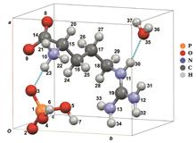
Tingting Sui, Xin Ju, Baoan Liu, Mingxia Xu, and Xun Sun
SignificanceAs a critical component of inertial confinement fusion (ICF), the research on the rapid-growth technology for large-sized deuterated potassium dihydrogen phosphate (DKDP) crystals has attracted significant attention worldwide. The control of growth and application costs for DKDP crystals as well as the regulation of the deuteration degree of the crystals and their performance are among the fundamental issues currently faced in improving load capacity.Neutron physics experimental methods are widely applied in materials science research with the following characteristics1) Neutrons interact with atomic nuclei through a non-monotonically varying scattering intensity function, making them suitable for determining light element positions in crystal lattices and distinguishing adjacent element positions; 2) Neutrons can differentiate between isotopes of the same element, enabling hydrogen-deuterium labeling which shows particular advantages in studying organic molecular materials and related fields; 3) Possessing magnetic moments, neutrons interact with atomic magnetic moments to generate unique magnetic diffraction, through which one can determine magnetic moment magnitudes and orientations of magnetic atoms in crystal lattices, serving as a crucial approach for studying magnetic structures; 4) Their significantly high penetration capability makes them particularly suitable for structural studies requiring specialized thick containers under extreme conditions like high/low temperatures and high pressure. The main limitations of neutron diffraction lie in requiring specialized intense neutron sources and the typical need for larger samples and longer data collection time due to insufficient source intensity. Currently, China possesses three major neutron science facilities: China Spallation Neutron Source (CSNS), China Mianyang Research Reactor (CMRR), and China Advanced Research Reactor (CARR).The current critical issues in enhancing load capacity and the hydrogen (H)-deuterium (D) network system of DKDP crystals are highly compatible with the research strengths of neutron physics methodologies. This paper, based on recent research results from both domestic and international sources, focuses on the application of neutron physics methods in the rapid growth technology of DKDP crystals and the study of laser damage. It also introduces our research progress in this field, points out research directions that should be continuously focused on, and looks forward to the application prospects of large-sized and high-quality DKDP crystals in the future.ProgressHigher performance standards have been imposed on critical optical components within laser transmission systems (Fig. 1). As ICF progresses toward higher energy levels in the future, the growth processes and defect control of DKDP crystals becomes research priorities, particularly exploring the relationship between process parameters and performance from microscopic perspectives, which forms the foundational scientific basis for advancing load capacity. The DKDP crystal structure is primarily dominated by ionic bonding, where each phosphorus (P) atom is coordinated by four oxygen (O) atoms arranged approximately at the vertices of a regular tetrahedron, forming PO4 groups, interconnected via H/D atoms (Fig.2). The unit cell parameters a and b increase with deuterium content, while parameter c shows no significant variation, resulting in relatively complete crystal structures for both low-deuterium and high-deuterium DKDP crystals (Fig. 3). Neutron diffraction methodology provides enhanced precision in quantifying H/D ratios and spatial localization within DKDP crystals. Experimental findings reveal that as the H—O and D—O bonds align parallel to the [100] and [010] crystallographic directions, deuterium content directly influences the lengths of O—O and P—O bonds in the structure (Table 1). The lighter mass of hydrogen facilitates quantum tunneling phenomena in O—H—…—O bonds, resulting in a more symmetric proton distribution between two oxygen atoms. This symmetry can lead to the formation of “quantum depolarization defects,” where PO4 groups fail to contribute to macroscopic polarization, thereby reducing the crystal spontaneous polarization strength and phase transition entropy. In contrast, D, with its heavier mass, exhibits a lower probability of quantum tunneling. D tends to deviate from the hydrogen bond center, forming an asymmetric distribution, which enhances the crystal spontaneous polarization strength and phase transition entropy. These microscopic characteristics manifest distinct differences in the optical field response of high-power laser systems, which is identified by the simulation (Fig. 4).Current challenges in crystal growth primarily include the following aspects1) Cone-column interface. Crystals grown via rapid growth methods exhibit distinct cone-column interfacial boundaries, which can induce phase jumps under optical field conditions, compromising homogeneity, and limiting their application in ICF engineering. Implementing controlled growth environments with structured constraints can improve crystal quality and growth efficiency (Fig. 5). 2) Nonuniform D distribution. Studies have investigated flow field states on crystal surfaces under varying growth conditions through hydrodynamic simulations, proposing optimized flow field strategies. Neutron imaging enables precise detection of H and D distributions in DKDP crystals, facilitating exploration of D-content variations in growth solutions and their impact on the growth process. Coupled with finite element simulations, this approach identifies correlations between growth parameters and flow field dynamics, thereby optimizing growth protocols to mitigate lattice mismatch, local overcooling, and deuterium inhomogeneity, ultimately enhancing crystal quality and laser damage resistance. 3) Residual stress in crystals. Three types of residual stresses arise during crystal growth. Neutron diffraction techniques allow noninvasive measurement of residual stress in DKDP crystals, revealing internal stress levels. Research indicates that macroscopic stress does not increase with deuterium content. Maximum lattice mismatch and microscopic strain occur when the mass fractions of H and D in the crystal are both 50%, with defects identified as the source of macroscopic residual stress. Additionally, developing real-time monitoring systems to track stress field dynamics and relaxation processes can provide critical feedback for refining key growth parameters.Conclusions and ProspectsFor significantly enhancing device load capacity, it is crucial of optimizing the entire operational workflow of DKDP components. As the initial stage of the workflow, crystal growth process optimization and fundamental research on ultraviolet damage response can systematically address engineering challenges. This paper focuses on the application of neutron physics methods in DKDP crystal growth and laser damage studies, where notable progress has been made. However, future work still faces multiple challenges. With the rapid development of large scientific facilities like CSNS, future neutron diffraction technology will advance towards higher resolution, faster dynamic response, and multi-physical field coupling analysis. Combined with X-ray and synchrotron radiation methods, these techniques can provide atomic-scale scientific insights for the regulation of DKDP crystal growth. Supported by theoretical simulations, closed-loop optimization of processes, structures, and properties is expected to achieve controllable preparation of large-size, low-stress DKDP crystals. Through collaborative efforts from Chinese researchers, DKDP crystals are anticipated to continue playing critical roles in laser fusion, high-energy laser systems, and emerging optoelectronic applications.
Sep. 13, 2025Vol. 52 Issue 18 1803006 (2025)
Rui Zhang, Xuping Wang, Bing Liu, Fudi Chen, and Jiyang Wang
SignificancePotassium tantalate niobate (KTa1-xNbxO3, KTN) crystals exhibit the largest quadratic electro-optic (EO, Kerr) coefficient among known materials. This extraordinary property enables electro-optic modulators to operate at driving voltages below 100 V, fundamentally overcoming the “kV bottleneck” that has historically constrained device miniaturization and energy efficiency in photonic systems. The technological implications are profound: such ultra-low-voltage operation is critical for portable biomedical imaging probes [e.g., endoscopic optical coherence tomography (OCT)], integrated optical communication chips, and compact three-dimensional (3D) sensing receivers where power consumption and footprint dictate feasibility. Beyond the Kerr effect, KTN’s tunable phase transitions and broadband optical transparency (250?5000 nm) offer unprecedented versatility in designing wavelength-agile devices for applications from near-infrared (NIR) telecommunications to mid-infrared (mid-IR) sensing. However, decades of research has revealed persistent barriers to practical adoption. The crystal’s infinite solid-solution behavior between KTaO3 and KNbO3 eliminates a congruent melting point, while sequential cubic→tetragonal→orthorhombic phase transitions during cooling induce severe compositional striations, cracking, and defects. Concurrently, challenges in understanding novel physical effects (e.g., space-charge-controlled deflection and ferroelectric domain engineering) have hindered practical applications. This review addresses these gaps by systematizing breakthroughs in crystal growth, property characterization, and device design, and synthesizes transformative advances in overcoming these challenges, establishing a unified framework to harness KTN’s full potential for next-generation photonics.ProgressKTN’s infinite KTaO3-KNbO3 solid-solution system and multi-phase transitions demand innovative growth strategies. For Czochralski method (Fig. 3), undercooling isothermal growth technique stabilizes the growth interface by minimizing temperature fluctuations, and double-crucible real-time feeding system continuously supplies stoichiometric material, suppressing compositional segregation. Combined with both technology, device-grade crystal up to 35 mm×37 mm×58 mm with Ta/Nb compositional uniformity better than 10-5/mm (Fig. 4) is achieved. For hydrothermal method, temperature-difference hydrothermal growth [Fig. 5(b)] enhances homogeneity by minimizing component segregation. Adding H2O2 eliminates blue color centers [Fig. 6(c)], though crystal size remains sub-centimeter.Systematic studies reveal composition-property relationships. Lattice parameter a increases linearly with Nb content x (Table 1). At x=0.37?0.39, KTN achieves optimal dielectric constant (εr>50000) near room temperature. The Kerr coefficient can be directly enchanced via the Curie-Weiss law. Cu2+/Fe3+ doping (0.5%?1% atomic fraction) enhances dielectric response [Fig. 15(d)] and optical homogeneity via trace-impurity-induced dielectric enhancement (e.g., Fe3+-oxygen vacancy dipoles polarize microregions, shifting TC by 60 ℃). Transverse deflection is observed in Cu∶KTN. A compositional gradient generates intrinsic refractivity variations. Coupling this with the Kerr effect under an external electric field produces laser deflection perpendicular to the field direction [Fig. 19(a)], contrasting conventional longitudinal models. Self-powered photoresponse in engineering “head-to-head” charged domain walls (CDWs) creates built-in fields for carrier transport. Cu∶KTN detectors achieve 5.23 mA/W responsivity (four orders higher than that of BaTiO3) (Fig. 12) and 250?1030 nm spectral coverage [Fig. 13(d)].Devices based on KTN crystal were well developed. Space-charge-controlled KTN beam deflectors achieve 250 mrad deflection at ±250 V [Fig. 18(b)], 80 times more efficient than LiNbO3 deflectors.A maximum modulation contrast model of KTN electro-optic modulators optimizes bias voltage, tripling contrast (0.106 versus 0.03). Room-temperature operation at 395 V half-wave voltage (Fig. 26) is enabled by giant Kerr coefficients (S11=2.2×10⁻¹⁴ m2/V2), orders of magnitude higher than those of conventional electro-optic crystals. Periodically poled KTN (PPKTN) exhibits 39% second-harmonic generation (SHG) efficiency at 1030→515 nm [Fig. 22(e)] and covers mid-IR (5→2.5 μm) band via quasi-phase matching, filling a critical gap in mid-IR laser sources.KTN-based devices are poised to enable wide-bandwidth, high-efficiency laser systems for lidar, OCT (Fig. 23), and ultrafast 3D imaging (Fig. 24). KTN-deflector-based swept-source systems scan at 100 kHz rates, resolving strawberry tissue structures at 7 μm axial resolution (100 nm wavelength sweep). Utilizing KTN’s optical isotropy and ultrahigh Kerr coefficient, polarization-modulated 3D lidar achieves 20° field-of-view with 4.4 cm precision at 15 m distance, 60% lower error than DKDP-based systems. KTN large-angle scanners enable synthetic aperture imaging with times wider scan angles than traditional EO crystals [Fig. 24(d)].Conclusions and ProspectsKTN crystals have demonstrated transformative potential in high-efficiency deflectors, low-voltage electro-optics, nonlinear photonics, and self-powered photodetection. Critical future directions include the following aspects. 1) Growth challenges: scaling hydrothermal crystals to device sizes and improving temperature stability during growth. 2) Device optimization: developing precise thermal control systems for Kerr-effect-based modulators operating near TC. 3) High-frequency mechanisms: exploring gigahertz modulation dynamics and field-induced phase transitions. 4) Emerging applications: leveraging scale-free optics and ferroelectric superlattices for quantum optics and integrated photonics. By resolving the dual frontiers of crystal homogeneity and physical understanding, KTN-based technologies are poised to redefine performance ceilings in high-speed optical modulation, energy-autonomous photodetection, and nonlinear frequency conversion.
Sep. 12, 2025Vol. 52 Issue 18 1803007 (2025)
Shuang Niu, Xiufei Hu, Dongyue Wu, Yong Yang, Muqing Zhang, Xiufang Chen, Rongkun Wang, Xuejian Xie, and Xiangang Xu
SignificanceAs a representative of third-generation semiconductor materials, silicon carbide (SiC) has emerged as a revolutionary substrate for high-power electronic devices, radio frequency (RF) components, extreme-environment sensors and future quantum technologies due to its outstanding properties, including a wide band gap, high thermal conductivity, high breakdown electric field, high electron saturation drift velocity, excellent chemical stability and high-temperature tolerance. The exceptional thermal conductivity of SiC is particularly critical for mitigating self-heating effects in wide-bandgap semiconductor devices such as GaN and Ga2O3. However, the performance enhancement and broad application of SiC-based devices face a fundamental bottleneck: conventional heteroepitaxial growth technologies, such as GaN/SiC, InP/SiC, and 3C-SiC/Si, inevitably introduce defects like high-density interface dislocations and cracks. These stem from significant lattice mismatch and differences in thermal expansion coefficients between materials, leading to substantial degradation in device performance. Moreover, high-quality crystal forms such as 4H-SiC cannot be directly epitaxially grown on mainstream substrates like silicon, which severely restricts material choices and limits the design freedom for heterogeneous integration.In this context, wafer bonding offers breakthrough solutions and demonstrates significant research value. Direct bonding techniques, such as surface-activated bonding and plasma-activated bonding, enable precise nanoscale control of the interface. These methods effectively circumvent issues related to lattice mismatch and thermal stress, confine defects to an ultrathin interfacial region, and largely preserve the intrinsic properties of functional materials. The core significance of this approach lies in three aspects. 1) Enabling homogeneous SiC bonding to construct three-dimensional power modules with low interface resistance and high thermal stability, thereby reducing the cost of large-size wafer production. 2) Unlocking the potential for heterogeneous integration of SiC. As a high-thermal-conductivity substrate, SiC can be bonded with materials such as Ga2O3, diamond, Si, GaAs, and InP, substantially improving heat dissipation efficiency. Leveraging mature silicon processes also promotes the development of high-density integrated circuits, while intermediate layer technologies further optimize interfacial performance. 3) Providing large-size, low-cost integration solutions. Therefore, in-depth research on SiC wafer bonding technology is not only critical to addressing the key bottlenecks of currently limiting SiC-based device performance and unleasing its vast application potential, but also serves as a core driver advancing semiconductor heterogeneous integration technology toward higher performance, broader material compatibility and lower cost. It holds profound strategic significance for the innovation and application of next-generation semiconductor devices.ProgressAs a key process in semiconductor manufacturing, the advancement of wafer bonding technology plays a vital role in enhancing device performance. This paper provides a systematic review of the research progress and application of SiC wafer bonding technology. First, the classification system of wafer bonding technologies is summarized, with a focus on two representative methods prominent in the SiC field. One is surface activation technology tailored for SiC material characteristics, including plasma activation bonding and room-temperature surface activation bonding. These techniques significantly reduce the required temperature and pressure for bonding through pretreatment. The other is Smart Cut technology, which combines ion implantation and bonding processes. This approach is particularly suitable for producing high-quality thin-film composite substrates, such as silicon-on-silicon carbide on insulator (SiCOI) structures, offering an ideal material platform for subsequent device fabrication. Second, this review details specific technical pathways for SiC wafer bonding. This includes heterogeneous bonding between SiC and other semiconductor materials, such as Si, Ga2O3, and InP, which aims to integrate the superior properties of different materials to expand device functionality. Also covered is homogeneous bonding between SiC wafers, which is essential for producing large-size, high-quality SiC substrates or specific structural devices such as micro electro mechanical system (MEMS) sensors. The paper examines various bonding methods along with key process parameters and associated challenges. Third, this paper highlights application examples of SiC-based devices that demonstrate the practical value of bonding technology. These include: MEMS sensors based on SiC homogeneous bonding, which exhibit high-temperature and radiation-resistant properties; photonic devices enabled by SiCOI structures, benefiting from its superior optical confinement; RF devices fabricated by bonding piezoelectric materials such as lithium niobate (LiNbO3) with SiC, combining efficient energy transduction with the high-frequency and high-power advantages of SiC; high-performance, low-cost SiC power devices produced by bonding high-quality single-crystal SiC layer with low-cost polycrystalline SiC or reclaimed single crystal SiC substrates via the Smart Cut process. Finally, the paper systematically summarizes the critical influence of these wafer bonding methods on the final bonding quality and the thermal performance of devices, offering valuable reference for researchers and engineers in selecting and optimizing bonding processes.Conclusions and ProspectsSiC wafer bonding technology effectively overcomes the thermal conduction bottlenecks and self-heating effects inherent in traditional semiconductor materials through heterogeneous integration. It enables low-damage bonding of SiC with Si, Ga2O3, InP and various insulating substrates, while also driving advances in homogeneous bonding toward larger wafer sizes and lower stress levels. This progress provides high-performance solutions for power devices, RF modules, MEMS sensors and photonic integration platforms. The core focus of future research lies in further uncovering the physico-chemical mechanisms at the bonding interface. There is a need to systematically elucidate the relationships among interfacial thermal resistance, contact resistance and bonding strength. Concurrent development of advanced processes, such as those enabling low lattice damage, submicron alignment, and reduced wafer warpage, is essential, with particular emphasis on defect control and energy band engineering in oxide intermediate layers. By establishing quantitative models that link the microstructural characteristics of the interface to its macroscopic electro-thermal-mechanical properties, collaborative optimization across multiple physical fields can be achieved. This will ultimately unlock the full potential of SiC wafer bonding in applications such as extreme-environment electronics, high-efficiency energy conversion, and high-speed optical communications, paving the way for a new generation of heterogeneous integrated material platforms that surpass the limitations of silicon-based technologies.
Sep. 25, 2025Vol. 52 Issue 18 1803008 (2025)
Song Zhou, Xiangxu Chai, Xiangbing Wang, Fang Wang, Bin Feng, Wei Zhou, Qihua Zhu, Dongxia Hu, and Ping Li
SignificanceLaser-driven inertial confinement fusion (ICF) stands as a pivotal approach in the quest for clean and virtually limitless energy, a concept first proposed in the 1960s. The fundamental principle involves using high-power lasers to symmetrically irradiate a fuel-filled target, compressing and heating the fuel to conditions where nuclear fusion can occur. A critical parameter in this process is the laser wavelength. It has been established that using short-wavelength ultraviolet (UV) lasers, typically generated through frequency conversion of infrared (IR) lasers, offers indispensable advantages. These include more efficient energy absorption by the target, better control over plasma instabilities, and reduced generation of undesirable high-energy electrons, all of which are crucial for achieving fusion ignition.The significance of this technology was brought to the forefront by the historic achievement at the U.S. National Ignition Facility (NIF) in December 2022, where a net energy gain from a fusion reaction was demonstrated for the first time. This milestone, which relied on converting 2.05 MJ of infrared laser energy into 3.15 MJ of fusion energy using third-harmonic generation (THG) in potassium dihydrogen phosphate (KDP) crystals, has profoundly boosted global confidence in the potential of laser fusion energy. As the field now looks beyond single-shot ignition experiments towards the development of a commercially viable fusion power plant, the requirements for laser drivers are evolving. Future laser fusion energy drivers must not only deliver high energy but also operate at high repetition rates (>10 Hz). This shift introduces a formidable challenge: managing the substantial heat deposited in the frequency conversion crystals due to laser absorption. Consequently, the development of nonlinear optical crystals with superior thermal and optical properties, coupled with advanced thermal management technologies, has become a critical bottleneck and a key research focus for realizing the dream of laser fusion energy.ProgressThis paper provides a comprehensive review of the progress in frequency conversion technology for laser fusion drivers, from the foundational developments in single-shot systems to the cutting-edge research for future high-repetition-rate energy drivers.The development of high-efficiency THG for large-scale ICF facilities has been a gradual process of engineering maturation. The nonlinear optical crystals used, primarily KDP and its deuterated form (DKDP), must meet stringent criteria, including high damage threshold, good optical homogeneity, and the ability to be grown to large size (approaching 400 mm). Early large-scale implementation on the Nova laser in the 1980s pioneered the use of a 3×3 segmented crystal array to overcome limitations in single-crystal growth size (Fig. 1). Employing a “Type-II/Type-II” phase-matching scheme, Nova achieved a THG conversion efficiency of over 60% (Fig. 2), providing the first major scientific validation of large-energy UV laser drivers. However, the segmented design introduced diffraction effects that degraded beam quality. The subsequent Beamlet laser, a prototype for NIF, introduced two key innovations: monolithic (single-piece) large-aperture KDP/DKDP crystals and a more robust “Type-I/Type-II” phase-matching scheme [Fig. 3(a)]. This new approach was less sensitive to polarization and temperature variations, consistently achieving over 70% efficiency and demonstrating superior stability [Fig. 3(b)]. The NIF facility inherited and scaled up this architecture, further refining crystal growth to achieve more than 80% THG efficiency with 42 cm crystals, setting the global standard for modern ICF drivers (Table 1).China’s Shenguang series of laser facilities have also made significant strides. Initially, these facilities faced a bottleneck where the THG efficiency would plateau and fall away from theoretical predictions at high input intensities (Fig. 4). To address this, researchers at the China Academy of Engineering Physics (CAEP) conducted a systematic analysis, identifying and precisely controlling several critical factors that contribute to phase mismatch. Key breakthroughs included improving the optic axis and deuterium content uniformity in DKDP crystals, optimizing crystal mounting techniques to minimize wavefront distortion, and developing an advanced temperature control system capable of maintaining uniformity to within 0.05 ℃, surpassing the NIF specification (Fig. 5, Table 2). The successful integration of these advancements led to a landmark achievement: a stable THG efficiency of over 80% was demonstrated on a 430 mm aperture system, with a peak efficiency of 82.8%, which was in excellent agreement with theoretical models (Fig. 6).Research has also extended to higher-order harmonics, as even shorter wavelengths could further enhance laser-plasma coupling. Significant progress has been made in fourth-harmonic generation (FHG). Researchers at CAEP developed an innovative scheme using non-critical phase matching (NCPM) in a 65% deuterated DKDP crystal within a converging beam. This technique achieved a remarkable 82% conversion efficiency from second-harmonic to fourth-harmonic light, generating over 180 J of UV output (Fig. 7). Fifth-harmonic generation remains challenging due to material limitations and higher susceptibility to optical damage and thermal effects, with current efficiencies around 14%?30%.For future fusion energy drivers, the primary challenge shifts to managing thermal effects in high repetition rate and high average power operation. Comparative studies of different crystals for second-harmonic generation (SHG) at 10 J/10 Hz revealed that while DKDP suffered from thermal dephasing, YCOB’s performance was limited by material quality, and lithium triborate (LBO) showed excellent performance, achieving 82% efficiency at 0.7 GW/cm2 (Table 3, Fig. 8). Building on this, the Bivoj/DiPOLE laser facility set a new world record, producing 50 J of third-harmonic energy at a 10 Hz repetition rate using large-aperture LBO crystals (Fig. 9). However, thermal gradients were still observed to evolve in the crystal over time, affecting the beam profile (Fig. 10). In China, research on a 100 Hz system demonstrated 3 J SHG output using an LBO crystal with a micro-channel cooling system that precisely controlled temperature to within ±0.05 °C (Fig. 11), demonstrating a scalable path towards kilowatt-level average power.Conclusions and ProspectsFrequency conversion technology is a cornerstone of mainstream laser fusion research. For single-shot, large-scale facilities like NIF, the technology based on KDP/DKDP crystals is mature, and China has recently demonstrated a breakthrough in achieving over 82% third-harmonic conversion efficiency through meticulous engineering controls. However, for the next generation of fusion energy drivers operating at high repetition rates, significant challenges remain. The thermal effects, optical damage, and long-term stability of nonlinear crystals under high average power are unresolved physical problems that require comprehensive breakthroughs.Future development should focus on three synergistic directions. First is the development of advanced crystal materials with lower absorption, higher damage thresholds, and larger nonlinear coefficients. This includes exploring alternatives like large-scale LBO and innovative concepts like composite “sandwich” crystal structures or artificially micro-structured materials. Second is the advancement of thermal management engineering. Techniques such as bonding crystals to high-conductivity heat sinks or using a gas-cooled, sliced-crystal-stack architecture must be perfected to handle kilowatt-level average powers. Third, the application of intelligent control systems is crucial. By integrating multi-physics modeling with AI-driven, real-time feedback from distributed sensors, future systems can dynamically predict and compensate for thermal distortions, ensuring stable, efficient, and reliable operation. The successful integration of these advancements will pave the way for a robust frequency conversion solution capable of meeting the demanding requirements of a laser fusion power plant.
Sep. 17, 2025Vol. 52 Issue 18 1803009 (2025)
Xu Chen, Huaize Qin, Yukun Song, Longxi Zhang, Jiankang Zhang, Yanling Cheng, Qilu Liu, Yuanhua Sang, and Jiyang Wang
SignificanceLithium niobate (LiNbO3) has played an essential role in the fields of electro-optic modulation and frequency conversion. In its early stages, it was primarily used as laser frequency-doubling devices and electro-optic modulators in optical communication systems. With the advancement of Ti-diffusion and proton exchange techniques, LiNbO3 devices were no longer confined to bulk configurations, facilitating the development of a range of integrated optical waveguide components. However, challenges in nanofabrication and constraints on integration density still persist. In the 21st century, with the explosive growth of information and data, traditional electronic computing is gradually approaching its physical limits. Emerging applications, including big data, artificial intelligence, high-speed networks, and virtual reality, are placing increasingly demanding requirements on computing devices in terms of performance, size, and energy efficiency.Owing to its exceptional electro-optic and nonlinear optical characteristics, LiNbO3 remains pivotal in traditional communication technologies, while also demonstrating irreplaceable value in emerging fields such as optical computing, artificial intelligence acceleration, and quantum information processing. In particular, the rise of the thin-film lithium niobate (TFLN) platform marks a new era for LiNbO3 as a platform for optical computing chips, which may have a tremendous impact on the future of information technology.TFLN, when combined with advanced nanofabrication techniques, has facilitated the development of compact, low-loss, high-speed photonic devices. TFLN has become a critical material platform for the development of high-speed electro-optic modulators, nonlinear photonic chips, and quantum photonic circuits. TFLN has gained increasing attention in the field of optical computing primarily due to the following reasons: Firstly, its strong electro-optic effect fulfills the high-speed modulation requirements for optical computing. Moreover, the low optical loss and high bandwidth of TFLN enable optical signal transmission over a broad frequency range with minimal attenuation. Finally, TFLN supports ultra-high integration density, making it suitable for constructing compact and miniaturized photonic integrated circuits (PICs).In recent years, the demand for computing processing speed has been approaching the performance bottleneck of electronic computers. Optical computing, as a computing system that relies on photons to process data, has advantages such as low energy consumption, large bandwidth, and fast response, making it one of the most promising disruptive computing architectures. Optical computing is of strategic importance to safeguarding information security and computational sovereignty. Lithium niobate materials and photonics have long been a significant research focus in China, and a series of significant breakthroughs have already been achieved in recent years. Therefore, a systematic review of the progress and prospects of LiNbO3-based optical computing is essential to guide future research and technological development.ProgressFigure 1 shows the microscopy image of the fabricated chip, which consists of three Mach?Zehnder modulators (MZMs) with various microwave signal line widths and device lengths. Figure 2 presents the schematic of the cross-section of the hybrid waveguide, as well as the multifunctional photonic integrated chip and its characterization system. An integrated lithium niobate (LN) modulator with segmented electrodes (designed to reduce the modulation voltage) has significantly enhanced the modulation bandwidth (Fig. 3). Figure 4 depicts the schematic of an MZM with a periodic CLTW (capacitively loaded traveling-wave) electrode. Figure 5 illustrates the architecture of a typical hybrid photonic neural network (PNN). Figure 6 shows a schematic of the proposed integrated photonic tensor core (IPTC), which consists of four physical components: lasers, two TFLN MZMs, and charge-integration photoreceivers. Figure 7 presents the conceptual schematic of a fully integrated optical convolutional neural network (OCNN), which uses an integrated photonic convolution accelerator (IPCA) fabricated on the lithium niobate-on-insulator (LNOI) platform and a micro-ring resonator (MRR) filter. Figure 8 shows an LN-based microwave photonics (MWP) processing engine, which consists of a high-speed electro-optic modulation block and a low-loss, multipurpose photonic processing section. The implementation of the photon ray-tracing core (PRTC) on the TFLN platform is shown in Fig. 9; the PRTC comprises four high-speed push-pull MZMs for parameter encoding, followed by coherent optical processing and detection components for binary result generation. A polarized TFLN waveguide was fabricated, and non-destructive high-resolution in-situ imaging technology was used for characterization (Fig. 10). Figure 11 provides the experimental setup for characterizing the photon pairs generated from the LNOI waveguide. Furthermore, a photonic chip with dimensions of 50 mm×5 mm×0.5 mm (capable of generating and manipulating entangled photon pairs) has been reported (Fig. 12). Finally, the experimental setup for measuring on-chip quantum interference is also showcased (Fig. 13); this setup can realize multiple photonic information processing functions, including on-chip quantum interference and photon demultiplexing.Conclusions and ProspectsThe emergence of TFLN has driven revolutionary advances in multiple fields, including optical modulation, nonlinear optical devices, optical computing, and quantum optics, thereby propelling the development of LiNbO3-based optical computing chips. Notably, critical performance metrics such as operational bandwidth, processing speed, and energy efficiency have undergone remarkable improvements. Importantly, some LiNbO3 optical computing chips fabricated in laboratories have already achieved performance levels suitable for market applications. However, the industrialization of LiNbO3 optical computing is still constrained by challenges in material fabrication, nanofabrication techniques, integration density, and system complexity. Bridging the gap from laboratory prototypes to commercial products will require coordinated efforts across materials science, optical engineering, and computing architecture.
Sep. 17, 2025Vol. 52 Issue 18 1803010 (2025)
Yunjia Bao, Ming Li, Zhongyang Liu, Zihao Wang, Kai Huang, Xin Xia, Rongbang Yang, Yulian He, Yuneng Chen, Kunfeng Chen, and Gongbin Tang
SignificanceIn recent years, lithium niobate (LiNbO3, LN) and lithium tantalate (LiTaO3, LT) thin films have attracted intense research interest due to their excellent electro-optic, piezoelectric, and nonlinear optical properties. By integrating these ferroelectric oxide films with silicon and other substrates, chip-scale photonic and acoustic devices have achieved remarkable performance improvements. This work reviews the state-of-the-art in heterogeneously integrated devices based on LiNbO3/LiTaO3 thin films, highlighting the importance of these platforms for next-generation communication, sensing, and quantum applications.ProgressConsiderable progress has been made in fabricating high-quality LiNbO3/LiTaO3 thin films using techniques like chemical vapor deposition (CVD), molecular beam epitaxy (MBE), pulsed laser deposition (PLD), magnetron sputtering, and smart cut, with each method presenting unique advantages and challenges in composition control, crystallinity, and scalability (Fig. 1, Table 1). For instance, CVD and sputtering enable large-scale production, while MBE and PLD offer atomic-level control for precision devices, and smart cut has become the industry standard for LiNbO3 on insulator (LNOI) substrates in commercial modulators and filters (Fig. 1). Domain engineering via femtosecond laser writing and piezoresponse force microscopy (PFM) allows nanoscale manipulation of ferroelectric domains, enhancing nonlinear and electro-optic properties (Figs. 2 and 3). In on-chip lasers, rare-earth-doped (e.g., Er-Yb co-doped) microring/microdisk lasers achieve ultra-low thresholds (~1 μW), while LN microresonator-based stimulated Raman lasers cover 1592‒1955 nm with sub-mW thresholds (Fig. 4). Optical parametric oscillators (OPOs) on LN films enable wide tuning (1.5‒3.3 μm), and Pockels-effect tunable lasers show record-high frequency sweep rates (2×10¹⁸ Hz/s) and ultra-narrow linewidths (<200 Hz), promising for coherent lidar (Fig. 5). Electro-optic modulators on LN/LT thin films feature reduced half-wave voltage (Vπ·L < 1 V·cm), ultra-high bandwidth (>100 GHz), and low insertion loss (<7.47 dB) via artificial microstructured electrodes and high-κ dielectric claddings (Fig. 6). LT modulators exhibit superior DC stability (e.g., <1 dB power fluctuation over 46 h) and lower photorefractive effects, outperforming LN in cost-effective scalability for high-speed communications (Fig. 7). In quantum photonics, LN/LT films enable efficient quantum frequency conversion (73% internal efficiency), single-ion Purcell enhancement (Purcell factor >170) in Er3+-doped photonic crystal cavities, and all-optical readout of superconducting qubits, eliminating cryogenic microwave components (Figs. 8 and 9). For acoustics, LN/LT thin-film-based surface acoustic wave/bulk acoustic wave (SAW/BAW) filters on platforms like LNOI, LN/SiO2/Si, and LN/SiC achieve 18.2% fractional bandwidth at 23.5 GHz with 2.38 dB insertion loss, and sub-1.2 dB loss at lower frequencies, addressing 5G/6G demands via optimized film orientation and electrode designs to suppress spurious modes (Figs. 10 and 11).Conclusions and ProspectsLithium niobate and lithium tantalate thin films have established a versatile platform for high-performance heterogeneous integration. Future research will focus on scaling to larger wafers, improving yield, and extending operation into new frequency ranges (e.g., millimeter-wave photonics). Advances in hybrid integration (e.g., LiNbO3 on insulator, LiTaO3 on insulator) and novel device architectures will further enhance functionality. Overall, the unique material properties of lithium niobate and lithium tantalate thin films—including high electro-optic coefficients, strong nonlinearity, and excellent thermal stability—position them to drive breakthroughs in high-speed, low-power photonic and acoustic devices. These advancements will pave the way for ultra-compact solutions in optical communications, lidar systems, and quantum photonic technologies, enabling next-generation applications in information processing and sensing.
Sep. 12, 2025Vol. 52 Issue 18 1803011 (2025)
Wenbo Luo, Qiuming Fu, Geming Wang, Qirui Wu, Zhibin Ma, Hongyang Zhao, Tingting Jia, Shiao Wang, Wenshu Liu, Minghe Wang, Ziyun Zhu, and Zhenxiang Cheng
SignificanceQuantum information technology (QIT), a key frontier field emphasized in China’s “14th Five-Year Plan” and the 2035 long-term development goals, serves as a core driver for leading the new round of scientific and technological revolution and industrial transformation. Its in-depth development is of great significance for enhancing national technological competitiveness, promoting innovation-driven development, and breaking through bottlenecks in traditional information technologies. As a critical material foundation for quantum devices, diamond stands out among numerous quantum materials due to its exceptional optical, mechanical, and electronic properties. It is one of the few materials capable of achieving stable manipulation of quantum states at room temperature, thus playing an irreplaceable role in the construction of high-performance quantum information processing systems. Notably, the nitrogen-vacancy (NV) color center in diamond—a point defect formed by a nitrogen atom and an adjacent lattice vacancy—exhibits extraordinary magnetic sensitivity at room temperature. This unique characteristic stems from its ability to realize precise manipulation of quantum states through laser polarization and microwave regulation, enabling high-precision measurement of weak magnetic fields even in complex environments. This endows it with broad application prospects in biomedicine, geological exploration, and industrial detection.In power systems, traditional magnetometers based on the principle of electromagnetic induction have long faced inherent limitations. For instance, they struggle to balance high precision and a wide measurement range, suffer from significant temperature drift during long-term operation, and are difficult to miniaturize for integration into smart grid sensor networks. These drawbacks severely hinder the advancement of intelligent monitoring of power grids, especially in scenarios such as high-precision DC current measurement and real-time status monitoring of power equipment. Against this backdrop, research on quantum magnetometers based on diamond NV color centers holds substantial scientific value and practical significance. It not only offers a novel technical pathway to overcome the bottlenecks of existing measurement technologies but also promotes the development of intelligent, integrated, and low-power-consumption measurement equipment. Furthermore, in-depth exploration of NV color center technology advances the practical application of quantum sensing, bridges the gap between fundamental quantum research and engineering applications, and lays a solid foundation for the innovative development of QIT in engineering fields such as energy, aerospace, and intelligent manufacturing.ProgressThis study first introduces the basic structure of NV centers and the principles of magnetic measurement (Fig. 1), with a particular focus on the continuous wave optical detection of magnetic resonance (CW-ODMR) method. It then details the fabrication processes of NV center diamonds, including high-pressure high-temperature (HPHT) synthesis (Fig. 4) and chemical vapor deposition (CVD) methods (Fig. 5), as well as subsequent processing steps. The advantages of ensemble diamond parameters are also discussed. Subsequently, the framework of the quantum magnetometer system is elaborated (Fig. 7), and the integration and development of quantum magnetometers are reviewed (Fig. 10). The current fabrication methods of diamond quantum magnetometers are summarized, highlighting the overall trends toward system integration, probe miniaturization, high sensitivity, and low power consumption. In the latter part of the paper, the current status of current sensors is detailed (Table 4). Traditional current transformers face certain limitations in achieving high-precision measurement, a wide dynamic range, and miniaturization of measurement probes, which significantly constrain the progress of smart grid research. To address these challenges, the application of quantum current transformers (QCTs) based on NV centers (Fig. 11) is introduced, and their use in power grid current transformers is explored, offering a novel solution for current monitoring. This study also compares different QCTs (Table 5) and further demonstrates the multifaceted application potential of diamond NV center quantum devices. Finally, the existing challenges of NV center magnetometers are discussed, and future research directions are proposed.Conclusions and ProspectsResearch on diamond NV center-based quantum magnetometers has made steady progress. The room-temperature quantum manipulation capability, high magnetic sensitivity, and relative stability in complex environments of these magnetometers have alleviated some of the limitations of traditional magnetometers and laid the foundation for high-precision magnetic field measurements—especially in power system monitoring. However, current challenges remain, including the high cost of high-quality diamond fabrication, difficulties in system miniaturization, and the need to improve measurement accuracy and noise suppression. Future efforts should focus on optimizing diamond growth and post-processing techniques to reduce costs and enhance the performance of NV ensembles, advancing system integration to improve portability and noise suppression capabilities, and exploring multi-physical-parameter sensing to expand application scenarios. These measures will facilitate the practical application of NV center technology in the field of quantum sensing.
Sep. 17, 2025Vol. 52 Issue 18 1803012 (2025)
Xiangyang Lei, Shuai Zhang, Qiao Xu, Shengfei Wang, Xueran Deng, Zhichao Liu, Wei Yang, Haohao Hui, Tianyu Wang, Rui Gao, Yuanhang Zhang, Feng Geng, Jianfeng Zhang, Hongju Ma, Jian Wang, Qinghua Zhang, and Fei Fan
SignificanceLarge-aperture potassium dihydrogen phosphate (KDP) and deuterated potassium dihydrogen phosphate (DKDP) crystals are the only nonlinear optical materials suitable for serving as frequency conversion elements and optical switches in high-power laser facility. However, their anisotropy, soft-brittleness, hygroscopicity, thermal sensitivity, and propensity for cracking impose significant challenges to ultra-precision manufacturing. Conventional grinding and polishing processes are prone to leaving abrasive particles embedded on the surface. These particles serve as precursors to laser-induced damage, significantly diminishing the laser damage resistance of the crystals. Consequently, the simultaneous attainment of full spatial-frequency bandwidth precision and a high laser-induced damage threshold (LIDT) constitutes a pivotal challenge in the advancement of high-power laser facility.ProgressTo address these challenges, an integrated technical route of “single-point diamond turning (SPDT) + sub-nanosecond laser conditioning + sol-gel coating” has been established. Significant progress has been made in the following areas.Ultra-precision cutting technology and equipment: an anisotropic constitutive model for soft-brittle crystals was developed to reveal the brittle-ductile transition (BDT) behavior during cutting (Fig. 1). Simulations identified the optimal cutting direction along 45° within the (001) plane and a BDT depth of approximately 150 nm. Through process optimization and the innovative design of an integrated vacuum chuck with variable hole density and active temperature control (Fig. 2), surface figure accuracy better than 4λ (λ=632.8 nm) and sub-nanometer roughness [root mean square (RMS)=0.59 nm] were achieved on large-aperture KDP crystals.Surface defects induced by fly-cutting, such as brittle indentations, cracks, protrusion pressure points, ballast, and plastic scratches, were systematically characterized (Fig. 4). Fluorescence microscopy (405 nm) revealed that defects like brittle indentations, cracks, protrusions, and ballast exhibit higher fluorescence intensity than defect-free regions, indicating stronger laser energy absorption and lower LIDT (Fig. 5, Table 1). An explosion simulation model was innovatively proposed to quantify the damage thresholds for different defect types and to elucidate the underlying damage mechanisms (Fig. 8). This model simplifies the complex multi-field coupling problem into a quantifiable explosive process, revealing that local mechanical strength and absorption capability are key factors affecting LIDT.Sub-nanosecond laser conditioning: the mechanisms underlying laser conditioning for the elimination or passivation of both point defects and structural defects were elucidated. A pulse width of 500 ps was identified as the optimal parameter within the 300?800 ps range, as it provides sufficient peak power for electronic excitation while exceeding the lattice heat transfer time necessary for thermal effects. After applying this offline conditioning process to 400 mm aperture DKDP crystals, under ultraviolet laser irradiation, the surface damage density was reduced from 5.02 to 0.55 pp/cm2, and the bulk damage density decreased from 2?3 to 0.3?0.8 pp/mm3 (Fig. 10, Table 2), marking a critical step toward engineering application.Sol-gel coatings: to enhance environmental stability and optical performance, multifunctional coatings were developed via sol-gel methods.Moisture barrier coatinga novel network-ball embedded structure was created by embedding hexamethyldisilane (HDMS)-modified SiO2 nanoparticles into a siloxane polymer matrix (Fig. 11). This structure yields a tunable refractive index (1.21?1.44), high hydrophobicity (contact angle increased to 109.4°), and exceptional moisture resistance (less than 0.1% transmission loss after 27 weeks at 80% relatively humidity).Antireflective (AR) coating: using methyltriethoxysilane (MTES) to seal surface pores after HMDS modification, an AR coating with low residual reflectance (less than 0.5%@355 nm), high LIDT (more than 20 J/cm2), and excellent oil contamination resistance (only 0.097% transmission drop after 20 weeks) was achieved (Fig. 12).Bilayer coating systema precisely designed bilayer system for dual-wavelength (527 nm & 351 nm) antireflection was realized. It combines a high-refractive-index moisture barrier layer and a low-refractive-index AR layer, exhibiting outstanding optical uniformity and environmental stability (0.7% transmission drop after 19 weeks in high humidity) (Fig. 13).Conclusions and ProspectsThis review comprehensively summarizes recent breakthroughs in ultra-precision manufacturing technology for large-aperture KDP/DKDP crystals achieved through an integrated process route. Significant advances in fly-cutting theory and equipment, defect characterization and suppression, laser conditioning, and functional coating design have collectively and notably enhanced the surface accuracy, laser damage resistance, and environmental stability of these critical optical components. Looking forward, future research should prioritize several key directions: 1) exploring novel processes such as ultra-precision polishing to further suppress mid-spatial-frequency ripples induced during machining; 2) developing multifunctional composite coatings that exhibit lower curing temperatures, higher LIDT, and extended operational lifetimes; and 3) establishing a full-process database that correlates manufacturing defects with damage performance, along with developing efficient, non-destructive online evaluation techniques for comprehensive performance assessment of large-aperture crystal components.
Sep. 25, 2025Vol. 52 Issue 18 1803013 (2025)
Peilun Ni, Rui Zhao, Xiaodai Yao, Xiaotian Lei, Hang Liu, Zijian Wang, Dehui Sun, Yongji Yu, and Guangyong Jin
SignificanceMid-infrared lasers operating in the 3?5 μm spectral band exhibit critical application value in spectroscopy, environmental monitoring, biomedical engineering, optical communications, and photoelectric countermeasures. This importance stems from their high atmospheric transmission within the atmospheric window and spectral alignment with numerous molecular absorption peaks, establishing them as a key research focus in laser technology. As one of the primary approaches for generating such lasers, optical parametric oscillators (OPOs) traditionally rely on discrete optical components, resulting in complex systems with limited potential for miniaturization. The revolutionary significance of self-optical parametric oscillation (SOPO) implemented through Nd3+-doped periodically poled neodymium-doped magnesium oxide-doped lithium niobate (Nd∶MgO∶PPLN) crystals lies in the monolithic integration of laser gain and OPO frequency conversion within a single gain medium. This breakthrough has opened up new avenues for developing compact, efficient, high-power all-solid-state mid-infrared lasers, garnering significant and sustained attention from both academic and industrial communities in recent years.ProgressThis paper systematically reviews research progress in mid-infrared self-optical parametric oscillator (SOPO) technology, with particular emphasis on Nd∶MgO∶PPLN crystal-based systems. It introduces the optical characteristics of neodymium-doped magnesium oxide-doped lithium niobate (Nd∶MgO∶LN) crystals, including polarization-dependent absorption spectra (Fig. 1(a)) and fluorescence emission profiles (Fig. 1(b)), along with their energy-level structure (Fig. 2). It elaborates how Nd3+ doping confers fundamental wave gain capability, while periodic poling enables efficient nonlinear frequency conversion, synergistically forming the physical foundation for Nd∶MgO∶PPLN as a self-frequency-converting crystal. The evolutionary trajectory spans from early dye-laser-pumped 1085 nm fundamental wave output to contemporary high-power, high-efficiency continuous-wave and pulsed 1084 nm/1093 nm outputs under laser diode (LD) pumping. Pivotal breakthroughs focus on suppressing thermally induced 1093 nm non-phase-matched polarized emission to achieve exclusive π-polarized 1084 nm fundamental light generation through innovative strategies, including thermally boosted pumping, multi-focus coupled pumping, and pulsed pumping techniques.Following the establishment of a high-quality fundamental light foundation, research focus has shifted toward optimizing frequency-converted output performance and characteristics through poling period design. Our research group has successively reported laser emissions covering critical application bands: the 1.5 μm eye-safe band, 2.1 μm molecular detection band, and 3.8 μm atmospheric window band, with targets on high power, high single-pulse energy, narrow linewidth, and programmable control. Representative achievements detailed include:(1) In the 1.5 μm band: 15.3 μJ pulses at 1512 nm under a 60 kHz repetition rate were achieved via dual-end pumping with intracavity acousto-optic Q-switching; 183 mW output at 1514 nm signal wave was obtained using multi-focus coupled pumping for thermal management during dual-spot pumping.(2) In the 2.1 μm band: degenerated 1.21 W output at 2168 nm was realized through intracavity acousto-optic (AO) Q-switching combined with optimized poling period design, followed by narrow-linewidth laser generation via Fabry?Pérot (FP) etalon integration.(3) In the 3.8 μm band: 3.04 W idler output at 3814 nm was obtained through pulse pumping combined with passive Q-switching; programmable pulse-burst generation was enabled by step-active Q-switching; 1.59 W average power output at 3834.3 nm under 28.4 W pump power (with wavelength stability and a tuning range of 29.4 nm) was yielded by thermally boosted pumping integrated with Cr∶YAG passive Q-switching and thermoelectric cooler (TEC) precision thermal control.This section culminates in a comprehensive developmental summary of Nd∶MgO∶PPLN crystal-based self-OPO technology, additionally reporting recent breakthroughs in pulse-pumped electro-optic (EO) Q-switched mid-infrared SOPO. Here, microsecond pulse pumping ensures full-range π-polarized 1084 nm fundamental light output, enabling stable mid-infrared idler generation through integrated electro-optic Q-switching—thus paving the way for miniaturized high-single-pulse-energy mid-infrared SOPO systems.Conclusions and ProspectsIn summary, self-optical parametric oscillator (SOPO) technology is progressively cementing its position as an indispensable methodology for mid-infrared laser generation, unlocking transformative pathways toward the realization of compact, lightweight, and high-power all-solid-state mid-infrared laser systems. The research trajectory demonstrates a coherent evolutionary logic: initial endeavors concentrated exclusively on attaining fundamental wavelength emission, subsequently advancing toward mitigating crystalline thermal effects to achieve precise polarization control of fundamental light, and upon establishing a robust foundation for fundamental wave performance, strategically pivoting toward optimizing quasi-phase-matched frequency-converted outputs for superior characteristics and enhanced functionality. Through meticulous poling period engineering, our research team has successively attained laser emissions spanning strategically critical spectral bands—specifically the 1.5 μm ocular-safe region, the 2.1 μm molecular fingerprint detection window, and the 3.8 μm atmospheric transmission band—while relentlessly pursuing performance benchmarks encompassing elevated power thresholds, augmented single-pulse energy densities, spectral linewidth narrowing, and programmable operational control.Notwithstanding these advancements, persistent challenges endure in practical deployment scenarios, notably insufficient suppression of thermally induced crystal distortions and limitations in further scaling pulse energy magnitudes. Future investigative priorities will emphasize enhancing systemic stability and amplifying output power metrics. Building upon extant SOPO experimental frameworks, the integration of miniaturized solid-state lasers as spatially optimized pumping sources presents a viable strategy for augmenting system compactness and functional integration. Capitalizing on the cognate electro-optic properties shared by Nd∶MgO∶PPLN and conventional lithium niobate (LN) crystals, experimental configurations could exploit Nd∶MgO∶PPLN to manifest intrinsic self-electro-optic Q-switching capabilities. Subsequent research initiatives should comprehensively explore the latent potential of Nd∶MgO∶PPLN crystalline platforms, with dedicated efforts directed toward developing multifunctional monolithic architectures that synergistically integrate pumping, optical gain, and Q-switching modalities within unified Nd∶MgO∶PPLN substrates—thereby catalyzing sustained technological progression of SOPO systems across academic research and engineering applications.
Sep. 17, 2025Vol. 52 Issue 18 1803014 (2025)
Huiqing Zhao, Dezheng Li, Jichuan Qiu, and Hong Liu
SignificancePiezoelectric materials possess intrinsic mechanoelectric coupling properties, allowing efficient bidirectional conversion between acoustic and electrical energy. This unique characteristic has opened transformative avenues in biomedical fields, particularly in brain science. Piezoelectric acoustic-electric conversion technology provides a powerful alternative, enabling non-invasive, precise, and wireless neural modulation and stimulation, which are essential for developing advanced brain-computer interface (BCI), neurological treatments, and neural regeneration strategies. This technology holds significant potential for treating challenging neurological disorders including Parkinson’s disease, epilepsy, and depression and for facilitating neural repair. Additionally, the integration of piezoelectric materials can enhance real-time diagnostics and therapeutic strategies, providing significant benefits in terms of patient safety, procedural efficacy, and reduced healthcare costs. The adoption of these materials can significantly enhance the quality of life for patients with chronic neurological conditions, enabling improved management, monitoring, and treatment outcomes.ProgressSignificant advancements have been achieved in applying piezoelectric materials within neuroscience, driven by continuous innovations in material science, device engineering, and biointerface design. In the inverse piezoelectric pathway, where electrical signals are converted into ultrasound, transcranial focused ultrasound stimulation (tFUS) has emerged as a leading non-invasive neuromodulation technique. Owing to its millimeter-scale spatial precision, controllable penetration depth, and highly tunable acoustic parameters, tFUS enables both targeted therapeutic interventions and the fine, reversible regulation of neuronal excitability and network activity (Fig. 4). To address the limitations posed by skull-induced acoustic scattering and energy attenuation, researchers have developed implantable piezoelectric ultrasound stimulators that integrate ultra-thin, flexible microprobes with localized stimulation capability. In animal models, these devices have been shown to precisely activate dopaminergic neurons and achieve on-demand dopamine release, offering new strategies for neuromodulation in deep brain regions (Fig. 5). Conversely, the direct piezoelectric effect, where ultrasound is converted into electrical signals, forms the foundation for wireless ultrasound-powered stimulation electrodes. For instance, advanced energy harvesters based on Sm-doped PMN?PT single crystals can provide stable, high-efficiency power delivery to chronically implanted electrodes, thereby eliminating infection risks, mechanical constraints, and frequent maintenance associated with percutaneous leads or battery replacements (Fig. 6). At the microscale, the advent of “neural dust” platforms, which are ultra-miniaturized wireless devices powered and interrogated by piezoelectric transducers, has enabled chronic, bidirectional neural recording and stimulation with minimal invasiveness, paving the way for long-term untethered neural interfaces (Fig. 7). At the nanoscale, ultrasonically activated piezoelectric nanoparticles (e.g., BaTiO?-based systems) can generate localized electric fields that modulate ion-channel dynamics, whereas piezoelectric nanostickers have demonstrated the ability to direct neural stem cell differentiation and accelerate tissue repair in traumatic brain injury (TBI) models via precise site-specific electrical stimulation (Figs. 8?9). The bidirectional acoustic?electric interconversion technology, enabled by both the direct and inverse piezoelectric effects, supports mutual transformation between ultrasound and electrical signals, with broad applications in cutting-edge fields such as ultrasonic medical imaging, ultrasonic biosensing, and ultrasonic brain?computer interfaces (BCIs). In imaging, flexible piezoelectric composite arrays allow high-resolution, real-time ultrasound visualization of cerebral vasculature and blood flow, while maintaining intimate conformal contact with the complex topography of biological tissue surfaces (Fig. 10). Building on these imaging capabilities, functional ultrasound (fUS) has been seamlessly integrated with brain?computer interface systems, enabling accurate non-invasive decoding of motor intentions with high spatiotemporal resolution and reliable multiday performance (Fig. 11). Furthermore, the development of injectable and biodegradable ultrasonic sensors has provided a wireless, real-time solution for monitoring critical intracranial physiological parameters such as pressure, pH, and temperature, significantly improving biosafety by reducing long-term implantation risks while maintaining high sensitivity and biocompatibility (Fig. 12). Collectively, these advancements underscore the versatile and transformative potential of piezoelectric acoustic?electric interconversion technologies, which encompass neuromodulation, wireless energy transfer, high-definition neural imaging, and precision biosensing, for both fundamental neuroscience research and the development of next-generation clinical therapies.Conclusions and ProspectsPiezoelectric materials represent a paradigm shift in brain science technology by enabling non-invasive neural imaging, wireless energy transfer, and precise neural modulation and stimulation. However, several challenges must be addressed to fully realize their clinical and practical potential. These include the neurotoxicity of lead-based piezoelectric ceramics, which must be mitigated by developing and optimizing lead-free or biodegradable piezoelectric materials to ensure biocompatibility and long-term stability in biological environments. Enhancing the acoustic energy coupling efficiency and power output of ultrasound-based wireless energy harvesting systems is also crucial to overcome limitations imposed by acoustic safety thresholds and improve operational effectiveness. Furthermore, improving the neural targeting efficiency and reducing invasiveness of nanoparticle-based stimulation systems through sophisticated surface modification techniques, optimized nanoparticle size, and alternative delivery methods such as intravenous or intranasal administration will be necessary. Future research directions will likely emphasize interdisciplinary collaboration, leveraging advancements in nanotechnology, materials science, electronics, and neural engineering to enhance system performance, targeting precision, and safety profiles. Integration with advanced computational modeling and artificial intelligence may further refine device performance and therapeutic accuracy. Continued innovation in these domains promises to facilitate the translation of piezoelectric acoustic-electric technologies from experimental stages to mainstream clinical applications, thereby significantly impacting neural modulation strategies, treatments for brain diseases, and the development of intelligent, minimally invasive neural interface devices.
Sep. 18, 2025Vol. 52 Issue 18 1803015 (2025)
Tao Yan, Xinhang Dong, Ju Lin, Yu Chen, and Min Luo
ObjectiveShort-wave ultraviolet lasers have attracted much attention due to their advantages of large photon energy, high spatial resolution, and excellent focusing ability, which are widely applied in the fields of laser processing, semiconductor inspection, medical diagnosis, data storage, and spectral analysis. Nonlinear frequency conversion is one route of realizing short-wave ultraviolet laser output. The generation of 266 nm through quadruple frequency converting from 1064 nm is comparatively mature at present, which benefits from the development of commercial β-BaB?O?(BBO) and CsLiB?O??(CLBO) crystals. However, the average output power of a 266 nm laser is relatively low at a high repetition rate, owing to the large walk-off angle and two-photon absorption of BBO. The serious deliquescence of CLBO crystals can be overcome by continuously heating at sealed condition, which limits the steady operation of a 266 nm laser. As a novel nonlinear optical crystal, RbLi(HC3N3O3)·2H2O (RLHCY) demonstrates the larger frequency doubling effect, the shorter phase-matching wavelength (calculated at 239 nm), and the higher laser induced damage threshold. More importantly, large-size crystals can be grown by solution method at low cost. This study is focused on crystal growth and optical properties of RbLi(HC3N3O3)·2H2O crystals.MethodsThe RLHCY crystal is grown by the solution method utilizing the raw materials of RbCl, LiOH·H2O, and C3H3N3O3 powders with mass fraction of 98%?99%. The solubility is measured by the way of multiple small quantities at different temperatures. The piezoelectric coefficient is determined by quasi-static piezoelectric coefficient measuring instrument to distinguish the positive and negative polarity. The rocking curve of (100) wafer is measured by X-ray diffractometer to evaluate the crystalline quality. The transmittance spectrum at 200?800 nm is obtained using ultraviolet-visible-near-infrared spectrometer in the step of 0.5 nm with a polished sample of 1.0 mm thickness. The refractive indices of (100), (010), and (001) wafers are measured by prism-coupling method at 407, 514, 636, 965, and 1547 nm. Consequently, the refractive index curve is fitted and the phase matching curve is calculated. The type I frequency-doubling device in dimension of 4 mm×4 mm×5 mm is adopted for the 266 nm output experiment.Results and DiscussionsThe solubility of RLHCY is increased with the temperature from 12.2 g (25 ℃) to 35.6 g (65 ℃) (Fig. 1). The optimized conditions are determined as the following: the growth temperature range of 50?25 ℃, the cooling speed of 0.5?1.0 ℃/d, and the rotation rate of 12 r/min. A transparent crystal is acquired in a large size of 50 mm×35 mm×20 mm (Fig. 2). Based on the plane orientating and the piezoelectric coefficient measurement, the growth rate is confirmed in the sequence of R[010]>R[001]>R[100]>R[00?1]. The full width at half-maximum (FWHM) of (100) X-ray rocking curve is 43.2″(Fig. 4), which indicates the excellent crystalline quality. The ultraviolet cut-off edge is around 238 nm and the transmittance at visible region is larger than 85% (Fig. 5). The calculated phase-matching curve demonstrates that the phase matched wavelength can be as low as 238 nm (Fig. 7). The 266 nm laser output is achieved under the 532 nm pumping (repetition frequency of 3 Hz, pulse width of 8 ns), using a type I device in a size of 4 mm×4 mm×5 mm. The conversion efficiency of 532 nm to 266 nm is about 2.8%.ConclusionsThis work focuses on the growth of RbLi(HC3N3O3)·2H2O by the solution method. A large crystal in a size of 50 mm×35 mm×20 mm is obtained under the optimal conditions of temperature range, cooling speed, and rotation rate. The FWHM value of X-ray rocking curve for (100) plane is 43.2″. The ultraviolet cut-off edge is measured to be 238 nm and the transmittance at visible region is higher than 85%. The laser output of 266 nm is realized using a type I frequency-doubling device. The conversion efficiency is about 2.8% from 532 nm to 266 nm. The output power and the conversion efficiency of 266 nm can be greatly improved by means of quality enhancement of both crystal and device.
Sep. 13, 2025Vol. 52 Issue 18 1803016 (2025)
Daofa Sun, Longnan Ma, Bo Yao, Hongkun Nie, Jinbao Xia, Jingliang He, and Baitao Zhang
ObjectiveSingle-frequency nanosecond-pulsed lasers find extensive applications in coherent radar, remote sensing, and nonlinear frequency conversion, owing to their inherently narrow linewidth, high temporal coherence, and high peak power. In conventional systems, high-energy single-frequency nanosecond pulses are generated by using a narrow-linewidth low-repetition-rate fiber laser as the seed source, and the seed pulse is then amplified by the diode-pumped solid-state amplifier stages. However, improving the overall amplification efficiency and reducing the numbers of required amplifier stages demand that the fiber seed laser delivers higher pulse energy without broadening its linewidth. In practice, increasing the pulse energy generally involves using a gain fiber with a larger core diameter (thus supporting multiple transverse modes), which in turn degrades the spatial beam quality. As a result, achieving high-energy output while preserving excellent beam quality remains a critical challenge for low-repetition-rate single-frequency nanosecond fiber lasers. To address this challenge, we propose the design of a low-repetition-rate high-energy single-frequency narrow-linewidth nanosecond fiber laser operating at a center wavelength of 1064.2 nm. The proposed design ensures that the pulse energy is significantly enhanced without compromising the beam quality, rendering the system well suited for applications in coherent radar, nonlinear frequency conversion, and related fields.MethodsThis study designs a fiber master oscillator power amplifier (MOPA) structure (Fig. 1), consisting of a single-frequency continuous fiber laser, pulse generation, and fiber amplifiers. For the single-frequency continuous fiber laser, a distributed Bragg reflector (DBR) single-mode laser with a linewidth of approximately 4 kHz is employed as the fiber seed source. To enhance the pulse energy after modulation, a double-clad fiber amplifier is used to pre-amplify the single-frequency continuous laser. A pre-shaped electrical signal waveform is applied as the modulation signal, and the single-frequency continuous laser is modulated into a pulse sequence with a repetition rate of 10 kHz and a pulse duration of 263 ns by an acousto-optic modulator (AOM). The resulting pulsed laser is coupled into an ytterbium-doped single-mode fiber (YSF) amplifier for energy amplification, and then enters a second AOM to reduce the repetition rate from 10 kHz to 100 Hz, followed by further pulse amplification using a pulse-pumped ytterbium-doped double-clad fiber amplifier with a 30 μm core diameter.Results and DiscussionsThe performance of the single-frequency continuous laser is first tested with a center wavelength of 1064.2 nm, a laser signal-to-noise ratio of 60 dB, and a 3 dB linewidth of 4 kHz (Fig. 2). After pre-amplification using a double-clad fiber amplifier, the laser is modulated by AOM-1 driven by an analog electrical signal, generating a pulsed laser with a repetition rate of 10 kHz and a pulse duration of 263 ns. After power amplification through a two-stage continuous pumping single-mode fiber amplifier, the laser is processed by a digitally-driven AOM-2 to reduce the repetition rate from 10 kHz to 100 Hz. At this point, the pulse duration is 307 ns and the single pulse energy is 8 μJ. The pre-shaped pulse waveform exhibits a tendency to broaden gradually in the fiber optic link (Fig. 3). To minimize the amplified spontaneous emission (ASE) and stimulated Brillouin scattering (SBS) effects during the amplification process, a large-mode-field double-clad fiber with a core diameter of 30 μm is used for the main amplification stage, with synchronous pulse pumping employed. The optical-to-optical conversion efficiency and the output laser signal-to-noise ratio (SNR) of the main amplification stage are shown at different pump pulse durations (Fig. 4). A maximum output power of 47 mW and a single-pulse energy of 470 μJ are achieved, with the laser pulse duration broadening to 452 ns and the SNR reaching 45 dB. The gain fiber of the main amplification stage is wound around a hollow copper column with a diameter of 6 cm to suppress the higher-order modes and enhance the amplifier stability in terms of power and polarization. At the maximum single-pulse energy, the laser performance is tested, with a beam qualityfactor (M2) less than 1.1. The power stability test shows a peak-to-peak jitter of less than 1%, with a root mean square (RMS) value of less than 0.4% (Fig. 5). A linewidth testing setup is built, and the time-domain data is processed through fast Fourier Transform (FFT) to obtain a 3 dB linewidth of 2.2 MHz for the laser pulse output (Fig. 6). The results show that the developed low-repetition-rate high-energy single-frequency narrow-linewidth nanosecond fiber laser meets the application requirements for fields such as coherent radar and nonlinear frequency conversion.ConclusionsThis study develops a low-repetition-rate high-energy single-frequency narrow-linewidth nanosecond fiber laser. The system employs a distributed Bragg reflector single-frequency continuous-wave fiber laser with 4 kHz intrinsic linewidth as the seed source. The continuous-wave output is modulated into pulsed operation at 10 kHz repetition rate through an analog-driven acousto-optic modulator. A cascaded continuous-wave-pumped ytterbium-doped single-mode fiber amplifier performs pre-amplification, followed by a digitally controlled AOM that precisely reduces the repetition rate to 100 Hz, generating a nanosecond pulse with 8 μJ energy and a custom-shaped temporal profile. The amplified pulse undergoes further energy scaling in a pulse-pumped ytterbium-doped double-clad fiber amplifier featuring a 30 μm core diameter. Through optimized pump pulse width and fiber coiling management, the system achieves linearly polarized single-frequency output with 100 Hz repetition rate, 452 ns pulse duration, and 470 μJ pulse energy. The laser demonstrates a 45 dB signal-to-noise ratio, near-diffraction-limited beam quality (M2<1.1), and 2.2 MHz spectral linewidth. This high-energy narrow-linewidth polarization-maintained nanosecond fiber laser with programmable temporal characteristics shows strong potential for coherent radar systems and nonlinear frequency conversion applications.
Sep. 13, 2025Vol. 52 Issue 18 1803017 (2025)
Heng Ding, Ning Zhang, Kui Wu, Fei Liang, Dazhi Lu, Shuxian Wang, Yongguang Zhao, Haohai Yu, Huaijin Zhang, and Jiyang Wang
ObjectiveThe 2-μm spectral region is critical for applications in precision machining, biomedical surgery (tissue absorption peaks), atmospheric sensing (molecular vibrational bands), and as a driver for high-harmonic generation (HHG) toward soft X-rays. Ultrashort pulse generation (<50 fs) in this band remains challenging for garnet-family crystals due to thermal effects from conventional ~0.8-μm pumping and limited gain bandwidth. Prior garnet-based lasers achieved only >50-fs pulses. Tm,Ho∶CNGG—a disordered calcium niobium gallium garnet—exhibits broad, homogeneous-free emission spectra owing to structural cation disorder (Nb5+/Ga3+ site randomness) and co-doping-induced inhomogeneous broadening, theoretically enabling few-cycle pulses. This work pioneers resonant in-band pumping at 1.7 μm to minimize quantum defects and thermal load while systematically exploring continuous-wave (CW), tunable, and mode-locking capabilities of Tm,Ho∶CNGG laser.MethodsThe experimental setup employed an X-folded cavity with astigmatism compensation (Fig. 2) pumped by a 1.7-μm Raman fiber laser focused to a 22-μm radius spot on a water-cooled (13 ℃) 3 mm×3 mm×6 mm Tm,Ho∶CNGG crystal. For CW and tuning studies, a 1.65-m-long cavity utilized two dichroic mirrors (ROC=-100 mm), a plane mirror (M3), and output couplers. Mode-locking was achieved using a semiconductor saturable absorber mirror (SESAM: 97% reflectivity, 1.5%?2% modulation depth) combined with Kerr-lens mode-locking; the SESAM replaced M3 with a second focus (beam radius ~65 μm), while two chirped mirrors (total GDD ~-125 fs2) compensated dispersion in the extended ~2 m cavity. Pulse characterization involved power meters, optical spectrum analyzers, autocorrelators, SHG-FROG, and stability diagnostics (oscilloscope, RF spectrum analyzer), with extra-cavity dispersion managed using a ZnSe plate (+730 fs2) and fused silica (-240 fs2).Results and DiscussionsStable mode-locked operation at TOC=1.5% yielded 42-fs pulses (6 optical cycles) at 2091 nm with a 113-nm FWHM bandwidth (Fig. 5)—the shortest pulse duration from any garnet crystal. SHG-FROG verified the pulse characteristics (<0.008 retrieval error, Fig. 8), confirming sech2 pulse profiles and linear spectral phase. The average output power was 105 mW (1.37-nJ pulse energy) at 76.6 MHz. Stability tests showed RMS power fluctuation <1.4% over 30 min [Fig. 9(a)], clean pulse trains [Fig. 9(b)], and RF spectra with >70-dB SNR [Fig. 9(c),(d)].ConclusionsThis study employs disordered Tm,Ho∶CNGG garnet crystal as the gain medium to investigate its continuous tuning and mode-locked laser performance. In continuous-wave operation, a tuning range from 1865 nm to 2132 nm was achieved, with a tuning bandwidth of 267 nm. In mode-locked operation, by balancing the group delay dispersion in the cavity, a 42-fs laser (corresponding to 6 optical cycles) was obtained at a central wavelength of 2091 nm with an output-coupler transmission of 1.5%, featuring a FWHM spectral bandwidth of 113 nm. This represents the shortest pulse width achieved based on garnet-series crystals, demonstrating the importance of the spectral inhomogeneous broadening induced by the structural disorder and co-doping mechanism of Tm,Ho∶CNGG crystals for broadband mode-locked spectrum generation, as well as the advantages of resonant pumping technology in few-cycle pulse generation. To achieve even shorter mode-locked pulses, Kerr media with high nonlinear refractive indices could be inserted into the cavity in the future to enhance the self-phase modulation effect, enabling nonlinear spectral broadening. Combined with dispersion management, this approach could further facilitate the generation of few-optical-cycle pulses.
Sep. 17, 2025Vol. 52 Issue 18 1803018 (2025)
Lin Li, Ke Lin, Li Shi, Peixiong Zhang, Zhenqiang Chen, and Yin Hang
ObjectiveAll-solid-state lasers exhibit excellent laser beam quality, stable output wavelength, broad spectral range, and high-power narrow-pulse output characteristics, making them suitable for military, medical, surveying and mapping, communications and other fields. The gain medium serves as the core component of a solid-state laser. A laser gain medium with a wide gain bandwidth is essential for achieving narrow pulse widths in mode-locked pulsed lasers. In recent years, significant research has focused on Yb3+-doped disordered laser crystals for fs-level ultrashort pulse generation. Rare-earth ion-doped disordered mixed crystals are widely employed in ultrafast lasers due to their broad emission bandwidths. However, the relationship between fluorescence bandwidth and the structural disorder surrounding the luminescent ions has not been systematically investigated or verified. Therefore, addressing the application requirements for near-infrared ultrashort pulse lasers, this study investigates the local structural distortions around luminescent ions in mixed crystals with different crystal structures. It further correlates these structural characteristics with the luminescent properties of the crystals to analyze the relationship between local structure and the bandwidth of near-infrared fluorescence spectra. The ultimate goal is to broaden the emission spectrum through structural engineering modulation, thereby developing novel gain medium materials promising for ultrashort pulse lasers.MethodsFirst-principles calculations were performed using the CASTEP code implementing the plane wave potential method based on density functional theory. The Perdew-Burke-Ernzerhof (PBE) functional within the generalized gradient approximation (GGA) was used to describe the exchange correlation potential between electrons. Based on convergence test, the 550 eV cut-off energy for all self-consistent field relaxation, and a k-grid with separation of 0.06/? was used in the first Brillouin zone integration to ensure the relaxation accuracy of 10-5 eV and 0.01 eV/?. To account for quantum effects arising from strong electron correlation effects in the d- and f-electron systems of Yb3+ ions with the electronic structure of [Xe]4f13, the Hubbard (U) values of the non-full shell f orbitals is set to 1.0 eV for correction.Yb3+-doped Y2(Ca,Mg)3(SiO4)3 (YCMS), Ca(Y,Gd)A1O4 (CYGA), and (Gd,Y)AlO3 (GYAP) crystals were grown using laser-heated pedestal growth (LHPG) method. The growth was conducted at a power of 39?43 W with a pull-rate ratio of 2.5?3. At the end of growth, the temperature was reduced to room temperature at a rate of 0.006?0.010 ℃/h to protect the crystals from large temperature variations. Single crystal X-ray diffraction and Raman spectra, fluorescence emission spectra were tested based on the optical polished samples. The spectroscopic properties (luminescent spectra of 950?1200 nm and fluorescence decays) were measured by the Edinburgh Instruments FLS920 and FSP920 spectrophotometers, under excitation of 922 nm. All measurements were performed at room temperature and other conditions were kept almost identical. The relationship between structural distortion and spectrum bandwidth broadening was analyzed based on structural changes such as cell parameters, cell volume, and distortion index.Results and DiscussionsThermodynamically stable configurations derived from first-principles calculations are used to comprehensively characterize the local structure disorder around luminescent ions in mixed crystal systems. This characterization employed quantitative parameters including the structural distortion index, polyhedral volume difference, unit-cell parameters, and unit-cell volume. Focusing on the cubic garnet-structured Yb∶YCMS, the relationship between the degree of polyhedral distortion of Yb3+ and the full width at half maximum (FWHM) of the emission spectra (Fig. 4) was analyzed. The increase in both the distortion index of the [YbO6]9- polyhedron and the unit-cell volume enhances lattice disorder surrounding Yb3+. This heightened disorder strengthens crystal field splitting, ultimately leading to broadening of the emission spectra. As evidenced in Table 1, the emission spectral FWHM of Yb∶YCMS crystals (89.85?103.10 nm), incorporating the matrix-regulating ion Ca2+, exceeds that of Yb∶YMS (87.26 nm).This comparison confirms the efficacy of matrix regulation for spectral broadening and suggests a positive correlation between fluorescence spectral bandwidth and structural modifications. Further structural analysis was conducted on Yb∶CYGA and Yb∶GYAP crystals belonging to different crystal systems. These analyses also indicated that varying ion ratios within the host lattice induce not only changes in the local Yb3+ coordination environment but also a degree of distortion within the entire unit cell. The luminescent ions in locally symmetric environments exhibit relatively long decay time, as shown in Tables 1-3. This study provides a comprehensive explanation for the relationship between structural distortion (both local and global) and key optical properties: spectral FWHM (positively correlated) and lifetime (negatively correlated), providing valuable guidance for the future design of optically tunable laser gain media.ConclusionsBased on the first-grown Yb∶YCMS, Yb∶CYGA and Yb∶GYAP mixed crystals with distinct crystal structures, the local geometric distortion around the luminescent ions was calculated using first-principles calculations. The structural distortion index and polyhedral volume difference are introduced as quantitative characterization parameters to describe the local structural disorder of the luminescent centers within these mixed crystal systems. It was found that as structural distortion increases, characterized by metrics such as the distortion index, ligand volume and unit cell parameters, the emission bandwidth undergoes inhomogeneous broadening. This finding verifies the effective broadening achieved through structural engineering in mixed crystal systems and provides valuable guidance for exploring novel gain materials for ultrashort pulse laser crystals.
Sep. 18, 2025Vol. 52 Issue 18 1803019 (2025)
Bohui Xu, and Zheshuai Lin
ObjectiveBirefringent crystals are indispensable for polarizing optics in applications such as laser modulation, UV detection, and quantum state control. Current commercial inorganic crystals (e.g., α?BBO, Δn=0.122 at 546 nm) exhibit limited birefringence, hindering the development of miniaturized optical devices, especially those operating in the solar-blind UV region (200?280 nm). Organic π?conjugated functional building units (FBUs) offer superior optical anisotropy due to strong electron delocalization and tunable weak interactions. This work aims to design a high-birefringence molecular crystal for solar-blind UV applications by strategically combining two anisotropic FBUs—melamine (C3N6H6) and cyanuric acid (H3C3N3O3)—through hydrogen-bond-directed assembly.MethodsThe melamine-cyanuric acid cocrystal (CNCO) was synthesized hydrothermally by reacting melamine and cyanuric acid (1∶1 molar ratio) at 180 ℃ for 10 h, followed by slow cooling. Phase purity was confirmed via powder X-ray diffraction (XRD), with experimental data matching theoretical simulations. Hydrogen bonding was characterized using Fourier-transform infrared spectroscopy (FTIR). The UV cutoff edge was determined from diffuse reflectance spectra, with the band gap derived via the Kubelka?Munk method. First-principles calculations were performed using the CASTEP package within the framework of density functional theory (DFT). The generalized gradient approximation (GGA-PBE) was used for geometry optimization, while the HSE06 hybrid function was employed to calculate electronic properties. Refractive indices and birefringence were derived from frequency-dependent dielectric functions. Hirshfeld surface analysis (Fig. 3) and differential charge density maps elucidated intermolecular interactions.Results and DiscussionsCNCO crystallizes in the I 2/m space group, forming a 2D layered structure via N—H…O (2.063—2.103 ?) and N—H…N (2.011 ?) hydrogen bonds between melamine and cyanuric acid molecules. These layers stack vertically with a spacing of 3.108 ?, stabilized by π-π interactions. Hirshfeld surface analysis confirmed strong in-plane N—H…O (proportion of contact area of 43.01%) and N—H…N (16.39%) hydrogen bonds, alongside out-of-plane π-π stacking (24.97%). FTIR revealed a significant redshift in N—H stretching vibrations (3362?3396 cm?1 vs. 3419?3470 cm?1 in pure melamine), validating strong H-bond-induced proton delocalization. UV spectroscopy showed a wide band gap of 5.06 eV (cutoff edge of ~250 nm) in CNCO, confirming its solar-blind UV transparency. Crucially, CNCO exhibited a giant birefringence of 0.508 at 400 nm—approximately four times larger than α-BBO (0.130 at 400 nm)—and 0.377 at 1064 nm. This surpasses most reported cyanurate or melamine-based crystals (e.g., K2Pb(H2C3N3O4)4(H2O)4, Δn=0.325 at 532 nm; (C3N6H7)BF4·H2O, Δn=0.37 at 546 nm). The exceptional Δn arises from synergistic effects: hydrogen bonds enforce parallel alignment of FBUs within layers, while π?π stacking enhances in-plane polarizability anisotropy.Electronic structure analysis (Fig. 6) revealed that the valence band maximum (VBM) is dominated by N 2p orbitals of melamine, while the conduction band minimum (CBM) comprises C 2p orbitals of the [C3N3] rings (from both melamine and cyanuric acid) and O 2p orbitals of cyanuric acid. The delocalized pπ electrons and anisotropic O 2p contributions underpin the huge optical anisotropy.ConclusionsThis work demonstrates CNCO as a record-high birefringence material (Δn=0.508 at 400 nm) for the solar-blind UV region. Its performance stems from the synergy of hydrogen bonds and π-π interactions, which enforce planar, parallel alignment of π?conjugated FBUs, maximizing in-plane polarizability. Experimental characterization (XRD, FTIR, UV-Vis) and DFT calculations consistently validate its wide band gap (5.06 eV), structural integrity, and giant birefringence. This study establishes hydrogen-bond-regulated molecular ordering as a powerful strategy for designing birefringent crystals, addressing the critical need for high-performance materials in solar-blind UV optics.
Sep. 17, 2025Vol. 52 Issue 18 1803020 (2025)
Chengcheng Liu, Dehua Wu, Qi Liu, Sujuan Sun, Xiaofeng Wei, Siwei Peng, Kai Beichao, Zhen Zhu, Junjun Du, Wanggen Sun, Chuanshang Fu, and Xiangang Xu
ObjectiveLaser diodes (LDs), leveraging their prominent advantages in high efficiency, long lifespan, and high repetition rates, have gradually supplanted flashlamps as the core pump source for solid-state lasers. LD side-pumped lasers introduce pump light via the crystal sidewalls. They boast an extended effective pump region that enables high-power pumping, thus emerging as an efficient solution for medium-to-high energy laser output. These lasers find extensive application in industrial processing, laser fusion, laser guidance, and other fields.However, thermal effects induced by the non-uniform gain distribution within the crystal, such as thermal lensing and thermally induced birefringence, severely constrain the performance of high-power laser systems. This limitation restricts large-aperture modules to operating below hundreds of Hz and impedes their utilization in high-repetition-rate scenarios.The primary objectives of this study are as follows(1) To probe into the factors that influence the gain field uniformity in a Nd∶YAG crystal with a diameter of 15 mm and a doping concentration (atomic fraction) of 0.6%; (2) To optimize the system structure to enhance the homogeneity of the gain distribution; (3) To alleviate thermal effects, thereby attaining high-power and high-beam-quality laser output.MethodsA theoretical model was established using ray-tracing methods. This model was employed to simulate and analyze the impacts of different LD arrangements (7-dimensional, 9-dimensional, and 11-dimensional) and the distances between LDs and the crystal on the gain field distribution (Fig. 2, Fig. 3).Based on the optimization results, an integrated LD side-pumped module was devised (Fig. 6). The module adopts an 11-dimensional annular array, with the distance from the LD to the crystal center being 21 mm. In each dimension, two LD bars are packaged using AuSn hard solder to form a ring-shaped unit structure (Fig. 4). The module is composed of eight serially connected ring structures and integrates a total of 176 LD bars. Additionally, it is equipped with a dual-coolant system for the independent thermal management of LDs and the crystal (Fig. 5).The experimental characterization encompassed wavelength consistency (Fig. 7), gain distribution uniformity (Fig. 9), thermal lens focal length (Fig. 10), and single-pass gain factor (Fig. 12).Results and DiscussionsThe designed 11-dimensional pump structure exhibited stable operation at a current of 140 A, a repetition rate of 500 Hz, and a pulse width of 200 μs. Under these conditions, the module achieved a peak pump power of 25 kW. Moreover, a 90% gain uniformity was realized across 90% of the crystal volume (Fig. 9), representing a notable improvement compared to the 7-dimensional and 9-dimensional configurations (Fig. 2). Additionally, a single-pass small-signal gain of 5.3 was attained (Fig. 12).Thermal lensing tests revealed that the focal length was 435 mm under high-power pumping (Fig. 10). Spectral analysis indicated that the wavelength deviations among all eight ring units were within -0.5 to +0.5 nm (Fig. 7). Meanwhile, the LD junction temperature remained at only 41.7 ℃ during operation at a 10% duty cycle, ensuring long-term reliability.ConclusionsThrough theoretical modeling and experimental validation, this study successfully developed an LD side-pumped Nd∶YAG module with a 15 mm diameter crystal, featuring high gain uniformity. The module caters to the requirements of high-repetition-rate operation at 500 Hz and delivers an integrated peak pump power of 25 kW.The optimized 11-dimensional pump configuration and the 21 mm pump distance design achieved a 90% gain uniformity. Concurrently, an extended thermal lens focal length (435 mm) and a high single-pass gain (5.3) were accomplished. This work furnishes a reliable pump solution for high-power solid-tate lasers in industrial and scientific applications.
Sep. 17, 2025Vol. 52 Issue 18 1803021 (2025)
Quan Yao, Yongkang Zhang, Xin Li, Daiying Wei, Bofeng Gao, Mingyang Zheng, and Xiuping Xie
ObjectiveLithium niobate (LN) has emerged as a cornerstone material in the fields of nonlinear optics and integrated photonics. While traditional bulk lithium niobate crystals have been extensively utilized for laser frequency conversion, they face significant limitations due to the walk-off effect and weak light field confinement during the process. These challenges necessitate extremely high pump light power levels to achieve substantial nonlinear conversion efficiency, making them less suitable for on-chip integration applications. The development of lithium niobate-on-insulator (LNOI) thin films has addressed these limitations through advanced bonding and thinning processes. LNOI not only retains the advantageous properties of bulk lithium niobate crystals but also offers a high refractive index contrast and the micron-scale light field confinement capability. Although Ti-diffused or proton-exchanged waveguides can achieve high frequency conversion efficiency, their relatively low damage thresholds (below 100 MW/cm2) significantly limit their applicability in high-power scenarios. In contrast, ridge waveguides directly fabricated in LNOI thin films through etching or other manufacturing techniques not only avoid introducing lattice defects but also maintain the excellent physical properties of the bulk crystals. While nanoscale thin film waveguides demonstrate ultra-high normalized conversion efficiency, their submicron mode field dimensions result in significant mismatch with standard fiber modes, leading to excessive coupling losses. To realize commercially viable high-reliability and high-power frequency conversion devices, the use of micron-scale thin film waveguides is imperative. The micron-scale LNOI ridge waveguides offer a promising balance between efficient nonlinear interaction and practical coupling performance, making them particularly suitable for demanding high-power applications. Further research should focus on optimizing their structural design and fabrication processes to fully unlock their potential in integrated photonics systems.MethodsAs illustrated in Fig. 1(a), the ridge waveguide utilized in this work features a ridge height of 7 μm, a ridge width of 7 μm, an etching depth of 3.5 μm, and sidewall inclination of 70°. The waveguide length is 15 mm, with a poling period of 18.18 μm for the 1560 nm second-harmonic generation (SHG) process. Our platform is based on z-cut LNOI thin film, comprising a 7 μm-thick LN layer, a 2 μm-thick SiO? layer, and a silicon substrate. The fabrication process involves two key steps: the periodically poling and the waveguide etching. As detailed in Fig. 2(a), the procedure begins with the deposition of aluminum layers on both sides of the LNOI wafer using electron beam evaporation. A periodic poling electrode pattern is then defined through spin-coating lithography, followed by the wet etching to reveal the electrode areas. Following the completion of the periodic poling process, a chromium layer is plated onto the sample surface to serve as a mask. The waveguide path is subsequently defined using spin-coating lithography, and the ridge waveguides are etched using the inductively coupled plasma. After completing the inductively couple plasma etching process, the chromium mask is removed using a chromium etchant solution. Finally, the waveguide sidewalls are polished to reduce the transmission loss, and both end facets of the waveguide are polished and coated with an anti-reflection layer to minimize the Fresnel reflection loss.Results and DiscussionsUnder low-power conditions, the normalized conversion efficiency of the SHG waveguide is measured to be 61%/(W·cm2). The relationship between the output power of the frequency-doubled light and the input power of the fundamental light follows a quadratic dependence. As the input power of the fundamental light increases, the output power of the frequency-doubled light scales linearly with it. Ultimately, an output of frequency-doubled light at 780 nm exceeding 5 W is achieved (Fig. 5). The internal conversion efficiency of the waveguide is determined to be 84.8%, while the overall device conversion efficiency reaches 52.6%. Analysis reveals that the residual fundamental light in higher-order modes and the temperature gradient generated by thermal effects at high power are the primary factors limiting the internal conversion efficiency from reaching 100%. Finally, a 24 h high-power stability test is conducted, which demonstrates excellent stability with the output power fluctuation within ±3%.ConclusionsThis paper presents a high-power periodically poled lithium niobate (PPLN) waveguide frequency conversion device with an all-fiber structure. Based on the 7 μm-thick magnesium-doped LNOI thin films, the PPLN ridge waveguides are fabricated using dry etching technology. Under an input power of 9.5 W at the fundamental wavelength of 1560 nm, the device achieves a SHG output of 5 W at 780 nm, corresponding to an overall conversion efficiency of 52.6%. Notably, after continuous operation for 24 h under high-power conditions, the SHG output power fluctuation remains within ±3%. Additionally, this study experimentally identifies the higher-order modes of the fundamental light as the principal factor constraining the device conversion efficiency from reaching its theoretical limit. The proposed single-mode condition provides a clear guideline for optimizing waveguide dimensions to enhance the frequency conversion efficiency. This high-power PPLN waveguide frequency conversion device successfully combines the high conversion efficiency with the low fiber coupling loss, delivering a significant output power. These advancements support the development of commercial integrated photonic devices and hold promising application prospects in quantum information processing and quantum light sources.
Sep. 13, 2025Vol. 52 Issue 18 1803022 (2025)
Qingguo Wang, Sen Kang, Fei Guo, Wei Chen, Yarong Lu, Wei Hua, Feng Wu, Ping Luo, Yongjun Dong, Dianjun Yan, and Jun Xu
ObjectiveAs an excellent oscillation and amplification medium for ultrafast, ultra-strong femtosecond lasers and high-power tunable laser systems, titanium sapphire (Ti∶Al2O3) crystals are among the laser crystals with the widest tuning range (700?1000 nm). Through the chirped pulse amplification (CPA) technology, laser pulse output of less than 10 fs can be achieved. They have extensive applications in high-energy physics, environmental pollutant detection, military defense, laser spectroscopy, and other fields, and become the preferred working medium for many ongoing ultra-intense and ultra-short laser engineering systems. The optical properties of Ti∶Al2O3 crystals are highly dependent on the concentration and uniform distribution of doped titanium ions (Ti3?). However, first, the coefficient of segregation of titanium ions in Al2O3 melt is only 0.16, which easily leads to the formation of axial and radial concentration gradients during crystal growth, resulting in optical inhomogeneity. Second, after titanium ions are doped, the viscosity of the Al2O3 melt significantly increases. The relatively slow convection of the melt leads to many scattering defects such as bubbles inside the crystal, making it difficult to prepare Ti∶Al2O3 crystals with uniform composition and high quality. Studies have shown that when the doping mass fraction exceeds 0.25%, it is easy to form Ti3?-Ti3? ion pairs and Ti?? impurity centers, significantly increasing the parasitic absorption in the 575 nm (visible light) and 800 nm (near-infrared) bands, and reducing the figure of merit (FOM) of Ti∶Al2O3 crystals. Therefore, it is extremely necessary to grow large-sized, high-quality and high-factor Ti∶Al2O3 crystals.MethodsHeat exchange method and Kyropoulos method are currently the most mainstream growth methods for large-sized and high-quality Ti∶Al2O3 crystals. The heat exchange method involves using liquid helium in the heat exchanger to remove heat, creating a longitudinal temperature gradient in the crystal growth zone from the bottom to the top. At the same time, the temperature gradient is controlled by adjusting the size of the gas (He cooling source) flow rate in the heat exchanger, adjusting the structure of the heat exchanger, and changing the heating power, which enables the melt in the crucible to gradually solidify from bottom to top into a crystal. In contrast, the Kyropoulos method is used to form temperature gradients in the axial and radial directions by adjusting the power of the heating zones around the crucible—for example, by cooling the top heater while heating the side heater. First, the raw material is heated to its melting point. Next, a seed crystal is brought into contact with the melt surface and slowly withdrawn. By controlling the cooling rate, the single crystals gradually solidify from top to bottom and finally grow into a whole single crystal. Through the self-designed heat exchange furnaces and the Kyropoulos furnaces, large-sized and high-quality Ti∶Al2O3 crystals with diameters of 380 mm×260 mm and 380 mm×360 mm are successfully grown.Results and DiscussionsLarge Ti∶Al2O3 crystals with 100 kg and the diameter up to 300 mm are grown successfully with the heat exchange method and the Kyropoulos method, respectively. The Ti∶Al2O3 crystals by the heat exchange method have a transparent red center, and under laser irradiation, scattered particles can be locally distributed. The color of the crystal gradually deepens along the direction of crystal growth, mainly due to the condensation of titanium ions, which leads to the gradual increase of doping concentration. In the central region of the crystal, the absorption coefficient at 532 nm from the seed crystal to the top of crystal gradually increases from 2.01 cm-1 to 3.98 cm-1. The Ti∶Al2O3 crystals by the Kyropoulos method also gradually deepen in color during the crystal growth process. The testing results of absorption coefficients at different heights from the seed crystal to the crystal bottom show that the absorption coefficient at 532 nm gradually increases from 0.6 cm-1 to 5.5 cm-1. The average stress of the wafer with 4 inch (1 inch=2.54 cm) diameter and 1 mm thickness is reduced from 183 nm/cm to below 10 nm/cm after hydrogen annealing. The full width at half maxima (FWHM) of the double swing curve is 14.04″, which shows that the sample lattice is intact and the single crystal performance is good. After polishing and coating, the laser energy amplification experiment is operated with 50 mm×35 mm sized samples, which achieves the laser energy amplification of 3 J , the pulse duration of 500 ps, and the peak power of up to 6 GW.ConclusionHigh-quality and large-size Ti∶Al2O3 crystals grown by the heat exchange method and the Kyropoulos method are now on the market.
Sep. 13, 2025Vol. 52 Issue 18 1803023 (2025)
Xiao Cao, Jianda Li, Yongchun Ren, Yi Huang, Qingsong Song, Youchenchen Zhou, Jian Liu, Jie Ma, Qingguo Wang, Huili Tang, Xiaodong Xu, and Jun Xu
ObjectiveThis work presents a detailed investigation of Nd∶YScO3 mixed sesquioxide crystals, addressing the urgent demand for advanced laser gain materials that combine superior thermal properties and excellent optical performance for high-power laser applications. The study is significant because it addresses the inherent limitations of pure cubic sesquioxides (RE2O3), which have excessively high melting point (>2350 ℃) that complicates crystal growth and raises production costs. The innovative approach centers on the YScO3 system, where the random distribution of Y3+ and Sc3+ cations creates structural disorder, allowing for considerable spectral broadening, a vital characteristic for ultrashort pulse generation. Since 2020, various rare-earth-doped YScO3 crystals (including Er, Yb, and Tm) have displayed impressive laser performance, yet the potential of Nd-doped variants for 1 μm applications remained unexplored. This work systematically evaluates Nd∶YScO3 as a novel gain medium, filling a critical gap in laser material development and providing new opportunities for highly efficient and thermally robust laser systems operating in the technologically important 1 μm spectral region.MethodsThe experimental approach utilized the edge-defined film-fed growth (EFG) method to produce 0.5% Nd∶YScO3 single crystals. This method was chosen for its capacity to ensure precise control over crystal dimensions and doping homogeneity. High-purity (99.99%) oxide powders (Nd2O3, Y2O3, Sc2O3) were accurately weighed according to the stoichiometric formula Nd0.005Y0.9975Sc0.9975O3, reflecting a nominal 0.5% Nd3+ doping concentration (atomic fraction), and thoroughly homogenized through extensive mechanical mixing. Crystal growth occurred in a meticulously controlled argon atmosphere (110 kPa) using a tungsten crucible heated to approximately 2140 ℃ via low-frequency induction, with the pulling rate consistently maintained at 4 mm/h throughout the process. Advanced monitoring systems provided real-time feedback for power adjustments based on weight change rates, ensuring stable growth conditions. Comprehensive characterization included inductively coupled plasma atomic emission spectroscopy for verifying doping concentrations, high-resolution X-ray diffraction for structural analysis, and double-crystal rocking curve measurements for quality assessment. Optical properties were extensively evaluated through absorption and fluorescence spectroscopy. This was followed by a detailed analysis using Judd?Ofelt theory to extract fundamental spectroscopic parameters. Laser performance testing under continuous-wave operation at 1.08 μm validated the material's practical utility.Results and DiscussionsThe Nd∶YScO3 crystals grown in this study exhibited exceptional quality, as evidenced by sharp, symmetric X-ray diffraction peaks (Fig. 2) and notably narrow rocking curve full-width at half-maximum values (Fig. 3). These findings indicate excellent crystalline perfection with minimal defects. Structural analysis revealed lattice parameters of a=b=c=10.235 ?, which closely followed Vegard’s law between Y2O3 and Sc2O3. This confirmed the formation of an ideal solid solution with random cation distribution. Spectroscopic characterization demonstrated an absorption cross-section of 0.14×10⁻²⁰ cm2 at the crucial 808 nm pump wavelength, alongside a particularly strong emission cross-section of 5.1×10⁻²¹ cm2 at 1084 nm, positioning it competitively with established Nd-doped laser materials. The fluorescence lifetime of the 4F3/2 energy level was measured at 314 μs, suggesting a high capacity for efficient energy storage. Most significantly, the crystal showcased outstanding laser performance by achieving continuous-wave output at 1.08 μm with a maximum power of 4.03 W and an impressive slope efficiency of 28.4%. This represents the first successful laser operation from Nd∶YScO3, validating its potential as a practical gain medium. These results significantly advance the field by demonstrating that the YScO3 host combines the advantages of traditional sesquioxides, such as excellent thermal properties, with the benefits of mixed cation systems (including spectral broadening potential), while maintaining competitive laser performance metrics.ConclusionsThis study established Nd∶YScO3 as a promising laser gain medium for 1 μm applications through thorough material development and characterization. The EFG method was effective in producing high-quality single crystals, despite the material’s high melting point, and structural analyses confirmed excellent crystalline. The spectroscopic properties, including favorable absorption and emission characteristics combined with efficient energy storage, position Nd∶YScO3 as a competitive alternative to traditional Nd-doped laser materials. The achievement of efficient continuous-wave lasing at 1.08 μm with a slope efficiency of 28.4% marks a significant milestone in laser material development, particularly for applications requiring high power and thermal stability. The unique structural characteristics of the YScO3 host, indicated by intermediate lattice parameters and random cation distribution, suggest additional potential for specialized applications needing broad emission spectra or specific thermal management properties. These findings not only broaden the range of available laser gain materials but also offer valuable insights into the fundamental relationships between crystal structure, spectroscopic properties, and laser performance in mixed rare-earth sesquioxide systems. Future research should focus on optimizing doping concentration, exploring different crystal orientations, and investigating the material’s potential for mode-locked operation to fully harness its spectral broadening capabilities. The successful development of Nd∶YScO3 crystals paves the way for advanced laser systems that combine high efficiency, excellent thermal properties, and unique spectral characteristics.
Sep. 17, 2025Vol. 52 Issue 18 1803024 (2025)
Wenqi Jia, Xiaoxuan Li, Ruyan Kang, Xiaoshan Wang, Ranyou Zhao, Zehan Liu, Guangzhi Zhu, and Zhiyuan Zuo
ObjectiveThe architecture of disk lasers exhibits significant advantages in terms of pump power and thermal management efficiency, representing a crucial development pathway for high-power and high-energy laser systems. However, bonding technology has long been a limiting factor in performance optimization. Traditional high-temperature soldering leads to solder splashing, secondary melting damage, and high thermal resistance, while direct bonding is difficult to implement widely due to challenges like lattice mismatch and stringent surface requirements. In comparison, the interlayer bonding offers a promising low-temperature alternative. Therefore, this study systematically investigates the influence of bonding interlayer thickness on the mechanical properties of Yb∶YAG/SiC disk laser device to optimize the bonding process for high-power disk lasers. It also explores how the interlayer thickness, precisely controlled by the spin speed, affects both the bonding strength and bonding stress. Establishing this quantitative relationship is essential for developing kilowatt-class disk lasers that achieve minimal thermal resistance along with maximum structural integrity.MethodsFollowing the process flowchart illustrated in Fig. 2, bonding experiments were conducted using SiC wafers with a diameter of 2.0 cm and a thickness of 1.5 mm as heat sinks, and Yb∶YAG disks with a diameter of 1.5 cm and a thickness of 0.15 mm (doped with 8% atomic percent of Yb) as the laser gain medium. During the process, the spin speed was adjusted to control the thickness of the bonding interlayer, which was subsequently quantified using spectroscopic ellipsometry. Spin coating was carried out for 60 s at spin speeds of 2×10³, 4×10³, 6×10³, 8×10³, and 10×103 r/min, with three replicates for each condition. After bonding, area mapping was performed on each disk device using a confocal micro-Raman spectrometer to obtain the two-dimensional (2D) stress distribution. The shift in the 261 cm-1 T2g peak was utilized to assess the average interface stress. Finally, tensile pull tests were performed using a universal testing machine to evaluate the bonding strength of the Yb∶YAG/SiC disk devices fabricated under each spin speed condition.Results and DiscussionsWith a fixed spin-coating duration of 60 s, the average thickness of the bonding interlayer decreases monotonically from 5.54 to 1.06 μm as the spin speed increases from 2×10³ to 10×103 r/min (Fig. 4). However, the rate of reduction significantly diminishes once the speed exceeds 6×10³ r/min. This phenomenon can be attributed to the combined effects of centrifugal force, shear-thinning behavior, and solvent evaporation: initially, centrifugal force is the dominant mechanism driving film thinning; as the interlayer becomes thinner, shear-thinning behavior and enhanced solvent evaporation become predominant phenomena. By correlating the measured interlayer thickness with mechanical performance: bonding stress (Fig.8) and bonding strength (Fig. 10), a coupling relationship of spin speed, bonding strength, and bonding stress is established. At a spin speed of 6×10³ r/min, the interlayer stabilizes at an average thickness of 1.86 μm, corresponding to the maximum bonding strength of 18.74 MPa and the bonding stress of 262.15 MPa. This moderate spin speed facilitates uniform layer formation with minimal defects. The resulting interlayer thickness is sufficiently substantial to ensure effective mechanical interlocking, while simultaneously thin enough to mitigate thermal expansion mismatch-induced stress.ConclusionsThis study systematically explores the influence of spin speed on interlayer thickness and its subsequent effect on the mechanical performance of Yb∶YAG/SiC disk laser gain devices. Experimental results demonstrate that a spin speed of 6×10³ r/min produces an interlayer thickness of 1.86 μm, achieving the highest bonding strength of 18.74 MPa and a bonding stress of 262.15 MPa. However, when the spin speed is increased to 8×10³ r/min or higher, the interlayer thickness decreases to no more than 1.42 μm, leading to excessive stress accumulation at the interface and a heightened risk of bonding failure. These findings establish an empirical basis for optimizing spin-coating parameters for Yb∶YAG/SiC interlayer bonding and provide valuable insights for improving the mechanical reliability of high-power disk lasers.
Sep. 12, 2025Vol. 52 Issue 18 1803025 (2025)
Wanggen Sun, Kaidi Zhao, Dehua Wu, Qi Liu, Junjun Du, Kang Chen, Chengcheng Liu, Chuanshang Fu, Wenjing Tang, Xiaofeng Wei, Sujuan Sun, Dechao Wang, Siwei Peng, Zhen Zhu, Wei Xia, and Xiangang Xu
ObjectiveDiode side-pumped laser modules (DSPLMs) with high-uniformity pump light fields hold significant application potential in space exploration, deep-sea research, handheld laser processing, and other fields. However, existing technical solutions fail to simultaneously achieve high pump uniformity and a high power-to-volume ratio, limiting the application of DSPLMs in these areas. Several methods have been proposed to improve the pump uniformity of DSPLMs, with the most common approaches including incorporating optical shaping, rotating the axial pump optical field, and increasing the pump distance. Although these methods can enhance pump uniformity to some extent, they suffer from drawbacks such as complex structures, high costs, increased volume, and reduced pump efficiency. The laser diode (LD), as the core pump source of DSPLMs, directly influences the module pumping performance through its optical field characteristics. Optimizing the LD optical field properties can reduce the production cost of high-uniformity DSPLMs, minimize their size, and improve pump beam utilization. In this study, we develop a DSPLM with a highly uniform pump light field by optimizing the LD epitaxial structure. The proposed module exhibits high pump uniformity, an excellent power-to-volume ratio, and high energy efficiency. Our approach provides a new direction for laser miniaturization.MethodsIn this study, we design and fabricate an LD with a strong optical field confinement structure and subsequently integrate it into a DSPLM. The performance of this module is then compared with that of a DSPLM based on a conventional LD structure. First, we design the epitaxial structure of the LD with strong optical field confinement. Numerical simulations are conducted to compare the far-field fast-axis divergence angle and the power-current-voltage (PIV) characteristics between the strong optical field confinement structure and the conventional structure. The results confirm that the divergence angle of the LD with strong optical field confinement is larger than that of the conventional LD. The epitaxial layers are grown on a GaAs substrate using metal-organic chemical vapor deposition (MOCVD). Subsequently, standard semiconductor fabrication processes including photolithography, development, metal evaporation, and cleaving are employed to produce the LD bars. The bars are packaged into a single-bar LD module using a heat sink, an insulator, and a cooling plate. The packaged LDs are then tested to verify that the strong optical field confinement structure indeed exhibits a larger divergence angle than the conventional structure while maintaining reliable long-term operation. Next, the LD bars are assembled into an LD pump array, which is integrated with a focusing cavity, a quartz tube, and an Nd∶YAG crystal to construct the DSPLM. Based on the ray-tracing method, simulations are performed for both epitaxial structures of the DSPLM to analyze the improvement in pump optical field uniformity achieved by using the LD with strong optical field confinement. The fluorescence distribution of the assembled DSPLM is experimentally measured to further validate the actual enhancement effect of the LD with strong optical field confinement on pump uniformity. Additionally, we characterize and compare the PIV characteristics, operating wavelength, small-signal gain, and store energy of both DSPLM configurations. The physical dimensions and mass of the DSPLM with strong optical field confinement are measured to calculate the pump power-to-volume ratio and the pump power-to-mass ratio.Results and DiscussionsSimulation results demonstrate that the strong optical field confinement epitaxial structure effectively increases the fast-axis far-field divergence angle. Compared with that of the conventional epitaxial structure, the divergence angle increases from 45.7° to 59.7°, showing a 14° improvement [Fig. 2(a)]. Experimental measurements confirm that the LD with strong optical field confinement indeed exhibits larger divergence angle than conventional LDs, reaching 60.5° [Fig. 4(a)]. Furthermore, this structure shows slightly better performance in other metrics, achieving a peak power of 220.5 W@200 A with an electro-optical efficiency of 61.9% [Fig. 4(b)]. The pump optical field simulation results of the DSPLM reveal that the strong optical field confinement structure achieves a pump uniformity of 87%, a significant improvement over the 82.3% obtained with the conventional structure (Fig. 7). Fluorescence distribution uniformity tests further verify that the actual pump uniformity of the DSPLM with strong optical field confinement reaches 88.4%, outperforming the 81.7% achieved with the conventional structure (Fig. 8). Additionally, the DSPLM with strong optical field confinement shows improvements in output power, small-signal gain (SSG), and stored energy, compared to the conventional structure, achieving a peak power of 2.98 kW, a maximum SSG of 15.9, and a maximum stored energy of 0.36 J [Fig. 9(a) and Fig. 9(c)]. With a volume of 468.16 cm3 and a mass of 1613.9 g, the DSPLM with strong optical field confinement demonstrates an excellent power-to-volume ratio of 14.1 W/cm3 and a power-to-mass ratio of 4.09 W/g, indicating its compact size and lightweight characteristics (Fig. 10).ConclusionsIn this study, we design and fabricate an LD bar with large fast-axis far-field divergence angle of 60.5° through a strong optical field confinement epitaxial structure. The single LD bar achieves a maximum peak power of 220.5 W with an electro-optical efficiency of 61.9%. By implementing this LD with strong optical field confinement in a DSPLM, we obtain fluorescence uniformity of 88.4%, superior to those with the conventional LD structures. The module demonstrates a laser output power of 2.98 kW @ 1064 nm, with an SSG of 15.9, a maximum stored energy of 0.36 J, a power-to-volume ratio of 14.1 W/cm3, and a power-to-mass ratio of 4.09 W/g. This approach of confining the LD optical field to increase the fast-axis far-field divergence angle and enhance DSPLM fluorescence uniformity effectively improves module performance while reducing its size and mass. These advancements enable the application of high-performance modules in space- and mass-constrained environments.
Sep. 13, 2025Vol. 52 Issue 18 1803027 (2025)
Baoli Wang, Zhihao Yan, Huabing Qin, Peipei Zhang, Chunming Sun, Peixu Li, Wei Xia, Dehua Wu, Qi Liu, Kang Chen, Zhen Zhu, Shuqiang Li, and Xiangang Xu
ObjectiveWith the expanding application of high-end fiber lasers across various fields, limitations related to mass, size, heat dissipation, and power consumption have become increasingly prominent in priority areas such as scientific research. There is a corresponding growing demand for fiber-coupled modules that are compact, lightweight, and possess a high electro-optical conversion efficiency as well as strong environmental adaptability to ensure stable and reliable operation. As a core component of a fiber laser, the fiber-coupled pump source module directly impacts the key performance of the fiber laser. High-end fiber lasers require semiconductor laser pump sources to possess the characteristics of lightweight design, compact form factor, high efficiency, high power output, wavelength locking in a wide temperature range, full current, and good environmental reliability. Therefore, an ideal fiber-coupled pump source should simultaneously incorporate all these characteristics to meet the diverse application requirements of fiber lasers across various scenarios. However, this presents a significant technical challenge, particularly in terms of the power-to-mass ratio, which still has considerable room for improvement. With the iterative upgrade of compact high-energy laser systems, bottlenecks such as output power, electro-optical conversion efficiency, lightweight design, and thermal management have become more pronounced, and breakthroughs are urgently needed to overcome external constraints in the field of research. Currently, traditional optical paths suffer from the issues of slow-axis collimation with long working distances, wasted optical path space, and large volume dimensions. Volume Bragg grating (VBG) wavelength locking causes beam deflection in the collimation direction and expansion along the slow axis, reduces coupling efficiency, and degrades numerical aperture of the output beam. Single-lens coupling suffers from low coupling efficiency due to aberrations. VBG has a high diffraction efficiency but low beam transmission, resulting in high losses and power attenuation that affect the coupling efficiency of the wavelength-locking module.MethodsOptimization of COS (chip on submount) devices based on high-power, high-efficiency 976 nm semiconductor laser chip packaging is needed to further improve the electro-optical conversion efficiency and reduce the slow axis divergence angle at high operating temperatures. Module adopts an optical-mechanical-thermal integrated balance design, brand-new slow-axis beam expansion collimating lens, optimized optical paths of fast-axis collimation, VBG wavelength locking, slow-axis beam expansion collimation, and separated coupling technology for fast and slow axes. At the same time, small-size and low-diffraction-efficiency VBG is used to develop wide-temperature and full-current wavelength locking. Finally,the combined use of all the above techniques makes the module to achieve a high-performance output . The light source is densely arranged, lightweight alloy materials are selected, a compact structure design is adopted, and thermal simulation optimization is performed to develop a lightweight module with a high power-to-mass ratio.Results and DiscussionsThe laser diode (LD) chips are packaged into COS devices to achieve a high-performance output. Through optimization, the electro-optical conversion efficiency at high-temperature operating points is improved by 2% [Figs. 3(a) and (c)], while the slow-axis divergence angle at high-temperature operating points is reduced by 0.5° [Figs. 3(b) and (d)]. Through the opto-mechanical-thermal integration design and simulation, the module size is 105 mm×33 mm×12.2 mm, and the module mass is 75 g [Figs. 11(a) and (b)]. Compared to traditional fiber-coupled modules, the volume is reduced by 60% and the mass is reduced by 70%. The fiber with a core diameter of 135 μm and a numerical aperture of 0.22 achieves a continuous output power of 280 W, an electro-optical conversion efficiency of 55%, a numerical aperture of 0.17, the center wavelength of 976.3 nm, and a spectral width of 0.4 nm [Figs. 12(a) and 12(b)]. The high-performance, lightweight 976 nm wavelength-locked fiber-coupled module developed in this paper has a power-to-mass ratio of 3.7 W/g and a power-to-volume ratio of 6.6 W/cm3.ConclusionsThis paper is based on a high-power, high-efficiency 976 nm semiconductor laser chip with an emitting area width of 190 μm and a cavity length of 4500 μm. At a current of 25 A, the output power reaches 25.5 W, with a voltage of 1.55 V, an electro-optical conversion efficiency of 68%, and a slow-axis divergence angle of 8° for 95% of the energy. The COS device integrates 18 LD chips of 976 nm and features a space-efficient packaging design and a balanced optical-mechanical-thermal integration. It employs slow-axis beam expansion collimating lens, optimized optical paths combining fast-axis collimation, VBG wavelength-locking, and slow-axis beam expansion collimation, and separated coupling technology for the fast and slow axes. Lightweight alloy materials and a compact structural design are selected along with thermal simulation optimization. A high-performance lightweight 976 nm fiber-coupled module is developed, achieving an output power of 280 W at a core diameter of 135 μm, an electro-optical conversion efficiency of 55%, a numerical aperture of 0.17, a center wavelength of 976.3 nm, and a spectral width of 0.4 nm. This achieves a power-to-mass ratio of 3.7 W/g and a power-to-volume ratio of 6.6 W/cm3, providing a stable and reliable laser for applications with constraints on mass, volume, and power consumption.
Sep. 16, 2025Vol. 52 Issue 18 1803028 (2025)
Chengkai Jiang, Kaiyan Pan, Xinyu Zhang, Qi Qin, Xiaopeng Hu, and Shining Zhu
ObjectiveThin-film lithium niobate (TFLN) photonic integrated circuits are driving the development of next-generation optoelectronic technologies. Due to the indirect bandgap nature of lithium niobate, the TFLN photonic integrated chips typically require off-chip light sources. Thus, grating couplers are key components for enabling efficient coupling between external light sources and the integrated chip. Existing research on TFLN grating couplers has primarily focused on oblique incidence configurations. While uniform gratings under angled incidence can achieve higher coupling efficiencies, they are less favorable during coupling and packaging processes due to the difficulty in accurately controlling the incident angle, which may introduce additional coupling losses. Vertical incidence is advantageous for device packaging; however, it often suffers from significant back-reflection caused by second-order Bragg diffraction. To mitigate this effect, efficient vertical coupling can be achieved by designing dual-layer gratings or incorporating a bottom reflector. However, such approaches often involve complex fabrication steps and may induce additional optical losses in other on-chip components. Therefore, it is of great significance to develop efficient vertical grating couplers on TFLN using standard films without metallic reflectors by carefully designing the grating structure and adopting relatively simple fabrication procedures. Such an approach will facilitate the integration of TFLN photonic chips with off-chip light sources.MethodsThis study presents the design of a non-uniform grating with a spatially varying period and duty cycle to achieve efficient vertical coupling. The grating structure is optimized using the L-BFGS-B algorithm, which is based on gradient descent. To ensure consistency between the design and the experimental results, the initial structural parameters are determined. A linearly tapered grating is then constructed to enable preliminary vertical coupling. The simulations are conducted using the finite-difference time-domain (FDTD) method with perfectly matched layer (PML) boundary conditions. The objective function in the inverse design is defined as the coupling efficiency of the vertical grating coupler, and a minimum feature size constraint of 300 nm is applied based on current fabrication capabilities. During optimization, the algorithm adjusts the widths of each grating tooth and trench according to the objective function, with gradients estimated via two FDTD simulations per iteration. The structural parameters are updated iteratively under the feature size constraint, and the process is repeated until 250 iterations are completed. After several rounds of simulation validation, 250 iterations are found to be sufficient to obtain the optimal structural parameters. Following the completion of the design optimization, simulations are also conducted to evaluate the impact of fabrication errors on the grating coupling efficiency.Results and DiscussionsSimulation results indicate that the designed vertical grating coupler achieves a coupling efficiency of -1.9 dB at 1550 nm. The grating is fabricated using electron beam lithography and ion beam etching. Scanning electron microscope (SEM) images reveal that the grating surface and sidewalls are clean and smooth. After fabrication, the device is characterized using the fiber-to-chip vertical coupling setup. Experimental measurements indicate a peak coupling efficiency of -4.3 dB near 1550 nm. The discrepancy between the measured and simulated results is mainly due to a fabrication-induced structural deviation of approximately 20 nm. Future improvements in fabrication processes may further enhance the device performance. In the 1525?1575 nm wavelength range, the measured spectral response aligns well with the simulation results. The vertical grating coupler proposed in this work is designed via an inverse design approach and fabricated using a simple process involving only a single lithography and etching step, without the need of heterogeneous material integration or metal reflectors. The measured coupling efficiency of -4.3 dB meets the basic requirements for photonic device testing and research. The 3 dB bandwidth of 25 nm is sufficient to support applications in lithium niobate based nonlinear photonic chips where single-wavelength lasers are used as the input light sources.ConclusionsThis work presents a vertical grating coupler on TFLN, designed using an inverse design method. The grating period and duty cycle are optimized using a gradient descent algorithm, and the coupler is fabricated through a single-step etching process. In the 1550 nm communication band, the fabricated coupler achieves a vertical coupling efficiency of -4.3 dB and a 3 dB bandwidth of approximately 25 nm. A deviation from the simulated efficiency (-1.94 dB) is observed, primarily due to fabrication limitations. Further performance improvements are expected with process optimization. The developed vertical grating coupler provides a practical and efficient solution for integrating off-chip light sources with TFLN photonic chips.
Sep. 18, 2025Vol. 52 Issue 18 1803029 (2025)
Peipei Zhang, Chunming Sun, Xiaodong Zhang, Wei Xia, Baoli Wang, Fuyang Ren, Kang Chen, Zhen Zhu, Shuqiang Li, and Xiangang Xu
ObjectiveAlGaInP-based red semiconductor lasers operating at 638 nm are vital for applications like displays and sensors. However, their long-term reliability is severely hampered by catastrophic optical damage (COD) occurring at the laser facets during operation. This COD stems from facet oxidation, which leads to non-radiative recombination centers, heat accumulation, and rapid power degradation. Conventional oxide facet coatings often suffer from insufficient thermal conductivity, optical absorption losses, and critically oxygen diffusion into the active region. Alternative materials such as ZnSe exhibit absorption at 638 nm. Aluminum nitride (AlN) is a promising candidate due to its wide bandgap, high thermal conductivity, excellent chemical stability, and transparency in the red spectrum. However, conventional deposition methods, such as magnetron sputtering or electron beam (E-beam) evaporation, often introduce lattice damage or leave interfacial transition layers that degrade performance. This study aims to develop a low-damage, low-temperature facet passivation technology using electron cyclotron resonance (ECR) sputtering to deposit AlN/Al?O? composite films, specifically engineered to suppress oxygen diffusion and enhance the COD resistance and reliability of 638 nm lasers.MethodsA low-temperature, low-damage facet treatment and deposition process is implemented using a solid-source ECR sputtering system. The process begins with in-situ Ar/N plasma cleaning under optimized conditions to achieve an atomically clean GaAs facet surface without lattice damage, utilizing low-energy ions controlled below 30 eV. Subsequently, without breaking vacuum, the thin composite passivation film is deposited. The key innovation is the direct deposition of 2 nm thick AlN films onto the cleaned facet via ECR sputtering using an Al target in Ar/N? plasma, followed by a 20 nm thick Al?O? layer. This AlN layer acts as a dense diffusion barrier. For the complete facet coating, conventional E-beam evaporation is then used to deposit standard anti-reflection (AR) and high-reflection (HR) stacks on top of this ECR-sputtered composite base layer. AlN thin films deposited by ECR on GaAs substrates under these conditions are systematically characterized using ellipsometry, atomic force microscope (AFM), and transmission electron microscope (TEM) to evaluate optical properties, surface morphology, and interface quality. Comparative devices are fabricated with facets coated solely by E-beam evaporation. Finally, 638 nm ridge waveguide laser diodes are fabricated using metalorganic chemical vapor deposition (MOCVD) grown epitaxial structures, cleaved, coated using both methods, packaged into TO-56 modules, and subjected to accelerated aging tests at 30 °C and a 1.2 A constant current.Results and DiscussionsEllipsometry confirms that the ECR-sputtered AlN film exhibits near-theoretical optical properties at 638 nm, with a refractive index of 2.13 and a zero extinction coefficient. AFM reveals exceptionally smooth and dense surface morphology for ECR-AlN, contrasting sharply with the columnar structures observed in E-beam deposited Al?O?. Crucially, cross-sectional TEM analysis demonstrates a sharp, defect-free interface between the ECR-AlN/Al2O3 composite film and the GaAs substrate, whereas E-beam deposited films show interfacial layers attributed to oxides or defects. Aging tests provide definitive evidence of the technology effectiveness. Devices with ECR-AlN/Al2O3 passivation show zero failures after 1000 h aging. Their output power degradation is less than 4%, primarily occurring early in the test, and crucially, their COD threshold remains highly stable at 1.91 W, representing only a 1% decrease from the initial 1.94 W. This corresponds to a power density of 6.3 MW/cm2 after aging, surpassing reported values for similar devices. In stark contrast, control devices with E-beam-only coatings suffer a 30% reduction in the COD threshold, dropping to 1.2 W, and exhibit a 40% cumulative failure rate after 1000 h. The superior reliability is directly attributed to the ECR plasma cleaning eliminating surface contaminants, the low-energy deposition preventing lattice damage, and the dense, oxygen-impermeable AlN film effectively blocking oxygen diffusion towards the quantum wells. These suppress interfacial oxidation, minimize the formation of non-radiative recombination centers, and prevent the thermal runaway that leads to COD.ConclusionsThis research develops a high-reliability facet passivation technology for 638 nm semiconductor lasers by integrating low-energy ECR plasma cleaning with the deposition of AlN/Al?O? composite films. The ECR process enables low-temperature and low-damage fabrication, producing AlN films with excellent optical properties and a sharp, defect-free interface. The ultrathin AlN film serves as a critical oxygen diffusion barrier. The technology effectively suppresses facet oxidation and COD, resulting in exceptional long-term stability under high-stress aging conditions. Devices incorporating this passivation exhibit minimal power degradation and maintain stable COD thresholds over 1000 h, significantly outperforming conventional E-beam coated devices. This ECR-sputtered AlN/Al?O? passivation provides a robust and effective solution for enhancing the reliability and lifetime of high-power 638 nm semiconductor laser diodes.
Sep. 13, 2025Vol. 52 Issue 18 1803030 (2025)
Xianglong Yang, Xixi Xiong, Jiaxin Zhang, Hongyu Shao, Xiufang Chen, Xuejian Xie, Rongkun Wang, Xiufei Hu, Guanglei Zhong, Guojian Yu, Guojie Hu, Muqing Zhang, Xiaobo Hu, and Xiangang Xu
ObjectiveSilicon carbide (SiC) exhibits excellent properties, such as high breakdown field strength, high saturation electron drift velocity, high thermal conductivity, and good chemical stability. These characteristics enable miniaturization and weight reduction of power modules, ushering in a new era for power devices. Having successfully transitioned from R&D to mass production, SiC materials and devices have advanced rapidly through industrial scaling. However, the price of contemporary SiC power devices is 2?3 times higher than that of their silicon-based equivalents with comparable specifications. This cost differential partially constrains the further market penetration of SiC technology. For the SiC industry, reducing costs while enhancing efficiency is a critical priority for the next developmental phase. The current mainstream wafer diameter of SiC is 6?8 inch. Transitioning from 8-inch to 12-inch substrates delivers over 125% greater usable area, substantially increasing the die yield per wafer by more than two-fold. Recent emerging applications such as augmented reality (AR) glasses and advanced integrated circuit (IC) packaging have further accelerated the market demand for 12-inch SiC substrates. However, as the crystal diameter increases, the manufacturing complexity increases exponentially. The principal challenges in fabricating 12-inch 4H-SiC crystals include the development of high-quality 4H-SiC seeds, nonuniform thermal field distribution, nucleation control exacerbated by superscaled dimensions, inefficient vapor-phase mass transport, evolution dynamics of precursor species in supersized growth systems, and intensified thermal stress leading to crystal cracking and defect propagation. This study aims to achieve an efficient diameter expansion of seeds in fabricating 12-inch n-type 4H-SiC substrates and characterize their properties.MethodsUtilizing a home-grown 8-inch (0001) carbon-face 4H-SiC seed crystal with a 4° off-orientation toward 112ˉ0, diameter expansion was achieved via the physical vapor transport (PVT) method. The thermal fields during 12-inch SiC crystal growth and diameter expansion were investigated using the Virtual Reactor simulation software. To expand the diameter of the crystals from 8 inch to 12 inch, a “trapezoidal” temperature field was designed and constructed with a small radial temperature gradient at the center and a large radial temperature gradient only within a certain range of the edges. This ensured expansion of the edges while reducing the overall stress on the crystal. To optimize the quality of the 12-inch crystals, a continuous flat temperature field was designed and constructed in conjunction with large-diameter seeds (>300 mm), without the need for diameter expansion, to optimize and improve the quality of the 12-inch seed. Following the acquisition of high-quality 12-inch seed, n-type 4H-SiC single crystals were grown under a controlled nitrogen gas flow. The as-grown boules were subjected to cylindrical grinding and end-facing to meet the standardized 12-inch diameter specification. These boules were sliced using laser cutting. The resulting wafers were subsequently thinned, polished, and cleaned to produce 12-inch n-type 4H-SiC substrates. The wafers were characterized by Raman spectroscopy, contactless resistivity measurement, automatic microscope scanning, high-resolution X-ray diffraction (HRXRD), and dislocation detection to analyze their polytype, micropipes, resistivity, crystal quality, and dislocations.Results and DiscussionsBuilding on our previously established 8-inch high-efficiency diameter expansion technology, this research leveraged a home-grown 12-inch SiC single-crystal furnace. Concurrently, numerical simulations and crystal growth experiments were employed to investigate the diameter expansion mechanism of ultra-large SiC single crystals. To balance the single-step diameter expansion magnitude and thermal stress compatibility in ultralarge single crystals, we engineered tailored thermal field profiles, flow field configurations, and diameter expansion hardware. Commencing with 8-inch SiC seeds, iterative crystal growth and processing cycles progressively scaled the crystal diameter to 12 inch. After achieving the diameter, multi-cycle crystal growth and processing optimized the crystalline quality in the expansion zone, ultimately enhancing the 12-inch seed integrity. Following the acquisition of high-quality 12-inch seeds, nitrogen gas doping was precisely regulated to achieve a 12-inch n-type conductive 4H-SiC ingot. A 12-inch n-type 4H-SiC substrate with a thickness of 560 μm was obtained through laser cutting processing. The performance of the 12-inch SiC substrate was characterized. Raman mapping indicated that there were no polymorphic inclusions, such as 6H and 15R, and the area ratio of the 4H polytype reached 100%. The micropipe distribution map indicated that there was no proliferation of micropipes in the edge expansion area, and the micropipe density was less than 0.01 cm-2. The resistivity distribution map showed a resistivity range of 20.5?23.6 mΩ·cm, with an inhomogeneity of less than 2%. The 5-point rocking curves of the (004) diffraction plane exhibited nearly symmetrical single peaks without multiple peaks, indicating that there were no small-angle grain boundary defects in the substrate. The average full-width half maximum of the 5-point rocking curve was 20.8″, which indicates good crystalline quality. Threading screw dislocation (TSD) density was 2 cm-2 using molten KOH corrosion.ConclusionsThe 12-inch 4H-SiC seed was obtained by the PVT method, expanding the boule diameter from 8 inch to 12 inch to obtain home-grown conductivity type 4H-SiC crystals. The 12-inch n-type 4H-SiC substrate with a thickness of 560 μm was processed through standard semiconductor processing steps including laser cutting, grinding, and polishing. The polytype of the entire wafer was 4H without other polytype inclusions. The micropipe density was less than 0.01 cm-2. The resistivity range was 20.5?23.6 mΩ·cm, with an average value of 22.8 mΩ·cm. The full-width half maximum (FWHM) of the rocking curve of the (004) diffraction peak was 20.8″. The TSD density was 2 cm-2. These results indicate the high quality of the 12-inch n-type 4H-SiC substrate. Further research is required to control the dislocation density in 12-inch SiC crystals and precise chemical-mechanical polishing process of the substrates.
Sep. 17, 2025Vol. 52 Issue 18 1803031 (2025)
Sheng’an Hu, Cuishan Wang, Xueting Jing, Junhua Zhao, Xiaoye Sun, Xiuhui Yue, Kai Jiang, Wenjing Tang, Jian Su, Mingsheng Xu, Wei Xia, and Xiangang Xu
ObjectiveThermal management has a crucial impact on the performance of high power semiconductor lasers. Poor heat dissipation can lead to an increase in junction temperature, a decline in output power, and a decrease in conversion efficiency, thereby affecting the operational stability and lifetime. Heat sinks play a crucial role in the heat dissipation of semiconductor lasers. In recent years, as the output power of semiconductor lasers continues to rise, higher demands are placed on their heat dissipation performance. As a third-generation semiconductor material, silicon carbide (SiC) has a theoretical thermal conductivity of 490 W/(m·K), much higher than that of aluminum nitride (AlN) ceramics [270 W/(m·K)]. It is regarded as an ideal material for manufacturing heat sinks for semiconductor laser packaging. Therefore, packaging semiconductor lasers with single crystal SiC heat sinks is an effective solution to improve the heat dissipation issues of high power semiconductor lasers.MethodsIn this study, we first design and fabricate single crystal SiC heat sinks with and without copper coated. After the heat sinks are fabricated, we select 640 nm and 915 nm chips from the same batch, package them with SiC heat sinks and compare them with laser diodes (LDs) packaged with standardized commercial AlN heat sinks. The 640 nm laser chip adopts the TO9 packaging form, and the 915 nm laser chip adopts the chip on submount (COS) packaging form. Finally, performance tests including power-current-voltage(P-I-V) and output wavelength are conducted on the 640 nm LD and the 915 nm LD. Based on the test results, the thermal resistance of the lasers is calculated.Results and DiscussionsThrough comparative experimental results, the maximum output power of the 640 nm LD packaged with the single crystal SiC heat sink is 4.8 W, which is higher than 4.3 W of the LD packaged with the AlN heat sink. Its threshold current and electro-optical conversion efficiency are also superior to those of the LD packaged with the AlN heat sink (Fig. 3). As the operating temperature increases, the output power of the former packaged with the single crystal SiC heat sink decreases by 0.78 W, while that of the latter packaged with the AlN heat sink decreases by 1.3 W (Fig. 4). In the wavelength test, the temperature drift coefficient of the LD packaged with the single crystal SiC heat sink is 0.24 nm/℃, while that of the LD packaged with the AlN heat sink is 0.261 nm/℃ [Fig. 5(a)]. As the operating current rises from 1 A to 2 A, the wavelength of the former increases by 1.23 nm, while the wavelength variation of the latter is 1.56 nm [Fig. 5(b)]. Through calculation, the thermal resistance of the LD packaged with the single crystal SiC heat sink is 3.32 K/W, which is lower than 5.45 K/W of the LD packaged with the AlN heat sink. In the catastrophic optical damage (COD) test, the LD packaged with the single crystal SiC heat sink achieves an output power of 8.7 W at 8 A, while the LD packaged with the AlN heat sink fails at 6.8 A (Fig. 6). The maximum output power of the 915 nm LD packaged with the single crystal SiC heat sink with copper coated is 1.9 W, higher than that of the LD packaged with the AlN heat sink with copper coated. The maximum electro-optical conversion efficiency is 64.9% at 30 A, which is higher than 62.1% of the latter (Fig. 7). In the wavelength test under different temperatures, it can be concluded that the wavelength drift coefficient of the 915 nm LD packaged with the single crystal SiC heat sink with copper coated is 0.358 nm/℃, which is smaller than 0.397 nm/℃ of the LD packaged with the AlN heat sink with copper coated (Fig. 8).ConclusionsIn this paper, single crystal SiC heat sinks with and without copper coated are developed based on single crystal SiC, and they are used to package and test the 640 nm and 915 nm laser chips. Through comparison, the 640 nm LD packaged with the single crystal SiC heat sink has an output power of 4.8 W and an electro-optical conversion efficiency of 42.7%, while the 915 nm laser packaged with the single crystal SiC heat sink with copper coated has an output power of 54.5 W and an electro-optical conversion efficiency of 64.9%. All performance indicators are superior to those of LDs packaged with AlN heat sinks. As the temperature increases, the wavelength drift of LDs packaged with single crystal SiC heat sinks is smaller. Therefore, packaging laser chips with single crystal SiC heat sinks is an effective method to improve the output power and the thermal management problems of semiconductor lasers.
Sep. 13, 2025Vol. 52 Issue 18 1803032 (2025)
Linlin Che, Qiu Chen, Bixue Li, Jianfei Zhang, Haoyu Fan, Xing Zhang, Xiufei Hu, Qingyu Li, Baitao Zhang, Xianglong Yang, Rongkun Wang, Xiufang Chen, and Xiangang Xu
ObjectiveThe growing demand for high-performance power electronics and wide-bandgap semiconductor devices has accelerated the need for large-diameter silicon carbide (SiC) substrates, particularly 12 inch wafers. Silicon carbide—endowed with exceptional thermal conductivity, a wide bandgap, and a high breakdown electric field—is a prime candidate for next-generation high-temperature, high-frequency, and high-power devices. However, SiC’s intrinsic properties (i.e., high hardness, brittleness, and low fracture toughness) pose substantial challenges to conventional wire-saw slicing methods, which suffer from low material yield, slow processing rates, and surface damage. More critically, traditional techniques struggle to meet the mechanical and geometric tolerances required for 12 inch wafers. Consequently, developing an efficient, low-damage, and scalable slicing technology for large-diameter SiC crystals has become a pressing priority. In response, laser slicing technology—especially ultrafast laser-induced internal modification—offers a promising alternative. Nevertheless, implementing this method on 12 inch SiC ingots introduces new challenges, including increased stress, warpage, and inhomogeneities across the larger crystal volume. This study aims to address these issues by integrating real-time focal correction, spherical aberration pre-compensation, and ultrasonic delamination to achieve high-quality slicing of 12 inch n-type 4H-SiC wafers.MethodsThe experimental substrate was a 12 inch (300 mm) diameter n-type 4H-SiC single crystal grown via the physical vapor transport (PVT) technique. The crystal had a thickness of 12 mm and was preprocessed using a dual-surface polishing method, resulting in a total thickness variation (TTV) of 17 μm and a surface roughness below 3 nm. A custom-built laser slicing system was employed, featuring a linearly polarized picosecond laser source with a wavelength of 1030 nm, a pulse width of 15 ps, a maximum power of 40 W, and an adjustable repetition rate of 100?500 kHz. The laser beam was expanded and focused using a high-numerical-aperture (0.67) objective lens with a working distance of 9.5 mm. To mitigate the significant refractive index mismatch between air (n≈1.0) and SiC (n≈2.6), a depth-dependent spherical aberration pre-compensation strategy was implemented using a spatial light modulator (SLM). The compensation phase maps were designed to optimize the focal spot size and reduce energy dispersion within the crystal volume. Real-time focal tracking was performed using a color confocal displacement sensor, which provided dynamic feedback to adjust the z-axis height via a piezoelectric actuator, synchronized with the surface topography. The optimized laser parameters were as follows: 5 W power, 100 kHz repetition frequency, 400 mm/s scanning speed, 200 μm inter-line pitch, and a target focus depth of 230 μm—resulting in a final modified layer at a depth of 680 μm. After laser processing, the ingot was immersed in deionized water, and ultrasonic waves (20?50 kHz) were applied to induce wafer delamination.Results and DiscussionsThe sliced 12 inch wafers were characterized for geometry, uniformity, and surface quality. The resulting wafers exhibited a TTV of less than 10 μm—representing a significant improvement over conventional techniques. The bow value was -14.07 μm, indicating a concave profile with stress concentration consistent with the scanning direction. Profilometry results revealed minimal height deviation along the laser scanning axis (0° direction), suggesting that focal correction effectively minimized depth fluctuations during internal processing. In contrast, larger deviations were observed in the feed direction (90°), attributed to cumulative stress effects between adjacent laser lines. White light interferometry (Sensofar S Neox) was used to analyze surface morphology at multiple wafer locations (center, edge, and facet) (Fig. 10). The central region (A) displayed uniform sawtooth structures with no evidence of interlayer delamination. By comparison, the wafer facet (B) exhibited minor structural irregularities, likely due to local refractive index variations and the need for dedicated compensation at the wafer edges. Regions C?F (edges) showed well-formed periodic crack arrays, reflecting stable energy distribution and laser?material interaction. The measured surface roughness (Sa) ranged from 3.25 μm to 3.93 μm, with the lowest values near the center (A) and slightly higher values at the edges (Table 1). Average step heights remained below 16 μm across all regions. The observed sawtooth and step structures resulted from localized thermal stress-induced cracking along the (0001) crystal plane—initiated by laser modification and propagated uniformly during ultrasonic delamination. These results highlight the importance of depth control and focal optimization for achieving uniform slicing outcomes. Simulation results further confirmed that an optimal processing depth of 230 μm yielded the shortest focal spot length (84 μm), minimizing kerf depth and reducing the need for post-slicing grinding (Figs. 4?5). When the preset and actual focal depths diverged by more than -20 or 20 μm, depth deviation increased dramatically, leading to potential slicing failure or multilayer separation.ConclusionsThis study reports the first successful slicing of 12 inch n-type 4H-SiC crystals using a combination of picosecond laser-induced internal modification and ultrasonic delamination. By implementing spherical aberration pre-compensation and real-time focal correction, high-precision laser slicing was achieved, producing wafers with a thickness of 680 μm, TTV<10 μm, and bow of -14.07 μm. The resulting wafers exhibited excellent surface uniformity, with Sa values between 3.25 and 3.93 μm and step heights below 16 μm. These findings confirm the feasibility of scalable laser slicing for large-diameter SiC substrates and provide key insights into laser?crystal interactions, laying a solid foundation for future industrial-scale wafering processes. The proposed methodology represents a significant advancement toward the efficient, high-yield manufacturing of next-generation SiC-based power devices.
Sep. 17, 2025Vol. 52 Issue 18 1803033 (2025)
Cheng Gan, Haiping Xia, Lizhi Fang, Liangbi Su, and Baojiu Chen
ObjectiveMid-infrared (MIR) lasers with wavelengths of 3?5 μm have significant application value in fields such as national defense, military use, biomedical applications, and gas sensing. However, current mainstream light source technologies, such as super-continuum laser methods and optical parametric oscillators, generally suffer from inherent drawbacks like complex system structures and low electro-optical conversion efficiency. In contrast, rare-earth ion-doped solid-state laser media—which offer high beam quality, good output stability, and a compact structure—are considered an ideal approach for achieving efficient 3?5 μm laser output. This study uses LiYF4 single crystals grown by the Bridgman method as the matrix, taking full account of their excellent optical and physicochemical properties. Additionally, holmium ions (Ho3+) are regarded as ideal active ions for this wavelength band due to their 5I5→5I6 energy-level transition, which corresponds to 3.9 μm emission. By successfully preparing Ho3+/Nd3+ co-doped LiYF4 single crystals, Nd3+ efficiently absorbs 808 nm LD pump light and, through inter-ion energy transfer, effectively excites Ho3+—alleviating the self-terminating effect of the lower laser level of Ho3+ ions and thus achieving 3.9 μm mid-infrared emission. The successful development of this single crystal provides a new material for the development of efficient and environmentally friendly 3?5 μm mid-infrared lasers.MethodsHigh-quality LiYF4 single crystals doped with Ho3+ (molar fraction: 0.6%), doped with Nd3+ (1.0 %), and co-doped with Ho3?/Nd3? (0.6%/1.0%) were prepared using the Bridgman method. The raw materials used were LiF, YF3, HoF3, and NdF?, each with a purity of 99.999%, in molar ratios of n(LiF)∶n(YF3)∶n(HoF3)∶n(NdF3)=50∶(50-α-γ)∶α∶γ (α=0,0.6; γ=0,1.0). The XRD patterns of the samples were measured using a Bruker D8 Advance X-ray diffractometer (Germany) with a scanning range from 10° to 90°. The absorption spectra of the crystals were determined using a Cary 5000 UV/VIS/NIR spectrophotometer within a wavelength range of 400 to 2200 nm. The mid-infrared fluorescence spectra and fluorescence decay curves of the samples were measured using FSP920/FSP980 mid-infrared fluorescence spectrometers and FLS920 UV-Vis-NIR fluorescence spectrometers. The doping concentrations of Ho3? and Nd3? ions in the grown crystals were measured by inductively coupled plasma atomic emission spectroscopy (ICP-AES).Results and DiscussionsHo3+ and Nd3+ ions successfully replaced Y3+ lattice sites in LiYF4 single crystals (Fig. 1, Table 1), indicating that the doping of Ho3+ and Nd3+ does not disrupt the LiYF4 crystal structure. Compared to Ho3+∶LiYF? single crystals, the higher spectral intensity parameter Ω? and fluorescence branching ratio of Ho3+ ions in Ho3+/Nd3+∶LiYF4 single crystals (Table 2) confirm that the co-doping of Nd3+ increases the asymmetry of the local crystal field environment around Y3+ ions and enhances the fluorescence emission efficiency of Ho3+ ions. The full width at half maximum (FWHM) values of Ho3+/Nd3+∶LiYF4 single crystals are 124 nm and 91 nm, which are higher than those of Ho3+∶LiYF4 single crystals (116 nm and 87 nm)—suggesting that the co-doping of Nd3+ ions facilitates the broadening of the mid-infrared laser emission range (Fig.4). Additionally, the emission cross-sections at 2.9 μm and 3.9 μm are 1.48×10?20 cm2 and 0.19×10?20 cm2, respectively (Fig. 5), demonstrating the significant laser output advantages of Ho3+/Nd3+∶LiYF4 single crystals. Finally, the energy transfer efficiency (ET1) from Nd3+∶4F3/2 to Ho3+∶5I5 is 91.42% (Fig. 8), the energy transfer efficiency (ET2) from Ho3+∶5I6 to Nd3+∶4I15/2 is 52.91%, and the energy transfer efficiency (ET3) from Ho3+:5I7 to Nd3+:4I13/2 is 61.43% (Fig. 9)—validating the efficient sensitizing and quenching effects of Nd3+ ions on Ho3+ ions.ConclusionsThe fully sealed crucible descent method is an appropriate process for growing high-quality Ho3+/Nd3+∶LiYF4 single crystals. Under 808 nm LD pumping, both 2.9 μm and 3.9 μm mid-infrared fluorescence emissions can be observed. The absorption cross-sections and emission cross-sections (for 2.9 μm and 3.9 μm, respectively) are 1.29×10⁻²⁰ cm2 and 1.48×10⁻²⁰ cm2, as well as 0.12×10⁻²⁰ cm2 and 0.19×10⁻²⁰ cm2—with effective emission bandwidths of 124 nm and 91 nm. The incorporation of Nd3+ ions enhances the lifetime of the Ho3+:5I5 energy level through energy transfer from Nd3+:4F3/2 to Ho3+:5I5 (transfer efficiency η=91.42%) and also promotes the energy transfer processes from Ho3+:5I6 to Nd3+:4I15/2 and from Ho3+:5I7 to Nd3+:4I13/2. These energy transfer mechanisms strengthen the 3.9 μm and 2.9 μm mid-infrared fluorescence emissions. The doping of Nd3+ plays roles in sensitization and deactivation. Therefore, Nd3+/Ho3+ co-doped LiYF4 single crystals are a promising medium for mid-infrared lasers.
Sep. 17, 2025Vol. 52 Issue 18 1803034 (2025)
Deqiang Li, Xun Sun, Yangfan Li, Huiru Sha, Jian Jiao, Biao Yang, Chongbiao Luan, Hongtao Li, Longfei Xiao, Xiufang Chen, and Xiangang Xu
ObjectiveAs a novel type of solid-state devices, photoconductive switches (PCSS) offer remarkable characteristics such as high power output (~MW), low jitter (~ps), ultra-fast switching time (~ps), and high repetition rates (>MHz). These advantages have led to their widespread application in diverse fields including pulsed power electronics, high-power microwave technology, and bioengineering. Compared to conventional photoconductive switches that rely on external energy storage capacitors, silicon carbide (SiC)-based integrated photoconductive switches exhibit superior performance, including faster rise times and narrower pulse widths, making them especially suitable for high-frequency and high-voltage signal transmission applications. This study systematically examines the performance variations of the energy storage capacitor unit within the integrated switch device under varying frequencies and under high-temperature, high-humidity conditions. Experimental results reveal that electrical breakdown in the energy storage capacitor unit under high electric field strength is primarily attributed to threading screw dislocation (TSD) presenting in the semi-insulating SiC substrate. Furthermore, simulation results confirm the correlation between the spatial distribution of screw dislocations and the voltage withstand capability of the energy storage capacitor unit. It is anticipated that the findings of this study will provide valuable insights for optimizing the structural design of integrated photoconductive switches and enhancing their performance under high electric field conditions.MethodsIn this study, we systematically investigated the conductive properties of integrated photoconductive switches. The experimental procedure was as follows: integrated photoconductive switch devices with varying capacitance values were fabricated, all with an electrode spacing of 1.5 mm. Initially, devices with capacitance values of 14 pF and 25 pF were tested. The experimental results demonstrated that the integrated photoconductive switch with a capacitance of 25 pF exhibited superior voltage conversion efficiency. To further evaluate the stability of the integrated switch device, the performance of the 25 pF energy storage capacitor unit was examined under high-frequency, high-temperature, and high-humidity conditions. High-frequency stability was assessed using an LCR meter (Keysight E4980A), while aging tests under high-temperature and high-humidity were conducted under reverse bias using a dedicated test system (DEVR-H3). Subsequently, the behavior of the 25 pF integrated photoconductive switch under high electric field strength was investigated. The breakdown mechanism was analyzed by integrating experimental data with theoretical simulations. Additionally, the correlation between the distribution of screw dislocations and the voltage withstand capability of the energy storage capacitor unit was explored.Results and DiscussionsThis study developed a SiC photoconductive switch device that combines switching and capacitor functions. It features an ultra-fast rise time (211 ps, measured from 10% to 90%) (Table 1), a minimum on-resistance of 5.3 Ω, and an output power of 6.5 MW (Fig. 3). Experimental results demonstrate that the energy storage capacitor unit integrated within the SiC photoconductive switch device exhibits high stability under high-frequency, high-temperature, and high-humidity conditions (Fig. 2). Through a combination of experimental and simulation approachs, it was determined that screw dislocations in the 4H-SiC substrate are the primary cause of electrical breakdown in the energy storage capacitor unit under high electric field strengths. Both experimental and simulation results confirm a clear correlation between the breakdown voltage and the distribution of screw dislocations (Figs. 4?6).ConclusionsIn this study, an integrated device based on 4H-SiC that combines photoconductive switching functionality was fabricated. The energy storage capacitor unit demonstrated high stability under high-frequency, high-temperature, and high-humidity conditions. The integrated photoconductive switching device achieved a maximum voltage conversion efficiency of 90.2%, a rise time of 211 ps, and a maximum output power of 6.5 MW. The results clearly indicate that screw dislocations in the 4H-SiC substrate are the primary cause of electrical breakdown in the energy storage capacitor unit under high electric field strengths. Through a combination of experimental and simulation approaches, the correlation between breakdown voltage and the distribution of screw dislocations was analyzed. Reducing the dislocation density in the 4H-SiC substrate is an effective strategy to enhance the voltage withstand capability of integrated photoconductive switch devices with integrated switching and capacitor functions. Additionally, avoiding the placement of energy storage capacitor units in regions with TSD aggregation during device manufacturing presents another viable approach to improve the voltage endurance of the switch.
Sep. 15, 2025Vol. 52 Issue 18 1803035 (2025)
Ming Shi, Zihan Li, and Haitao Huang
ObjectiveBenefiting from the maturity of 0.8 μm laser diode pump sources and a diverse range of laser materials, thulium-doped lasers serve as the mainstream solution for achieving 2 μm laser sources. However, the 0.8 μm pumping scheme suffers from a large quantum defect. Even with the use of concentration-dependent cross-relaxation processes to enhance the populating efficiency of the upper energy level, the slope efficiency of 0.8 μm laser diode (LD)-pumped thulium-doped lasers generally remains below 50%. According to the absorption spectra of thulium-doped media, these materials exhibit strong ground state absorption (3H6→3F4) at 1.6?1.7 μm, which enables an in-band pumping scheme and thereby enhances the operation performance of 2 μm thulium-doped lasers. Although using 1.6 μm fiber or solid-state lasers as pump sources can precisely match the strongest absorption peak of thulium-doped media in the 1.6?1.7 μm band, it inevitably increases the complexity and the cost of 2 μm thulium-doped laser systems. Additionally, 1.6 μm Er-doped fiber or solid-state lasers typically utilize pump sources based on 0.8?1 μm laser diodes. If the conversion efficiency of the 1.6 μm pump source is also taken into account, the overall conversion efficiency of the 2 μm thulium-doped laser with 1.6 μm laser pumping will also be significantly reduced. Emerging application scenarios like transparent plastic welding have driven the commercialization of InP-based long-wavelength laser diodes at 1.7 μm, which provide cost-effective in-band pump sources for 2 μm thulium-doped solid-state lasers.MethodsThe laser experiment employs LD with a central wavelength of 1700 nm (linewidth of 5.3 nm) as the in-band pump source. The output fiber of LD has a core diameter of 400 μm and a numerical aperture (NA) of 0.22. Significant absorption of thulium-doped media at 1700 nm is a prerequisite for achieving in-band pumping. Therefore, Tm∶YAG and Tm∶YAP crystals are selected as laser media. Tm∶YAG crystals cut in the [111] crystal orientation and Tm∶YAP crystals cut in the b-axis are used. The doping atomic fractions of both crystals are 2%, and the dimensions are both 4 mm×4 mm×8 mm. Anti-reflection films at laser wavelength are coated on the two light-transmitting surfaces of 4 mm×4 mm. The resonant cavity has a length of 15 mm. The side of the input mirror (IM) facing away from the resonant cavity is coated with an anti-reflection (AR) layer at 1650?1750 nm, and the other side is coated with a high-reflection (HR) layer at 1900?2150 nm (reflectivity of >99.5%). The output coupler (OC) has a transmission of 5% across the 1900?2100 nm band.Results and DiscussionsFor the 1700 nm LD-pumped Tm∶YAP laser, oscillation initiates at the absorbed pump power of 1.56 W. When the absorbed pump power is increased to 10.7 W, a maximum output power of 7.13 W at 1987 nm is achieved, corresponding to a slope efficiency of 80.5% (Fig. 7), which is increased by 78.5% compared to that achieved in 785 nm LD pumping. The beam quality of the 1700 nm LD-pumped Tm∶YAP laser at the maximum output power is measured with the beam quality factors being Mx2=1.73 and My2=1.87. The 785 nm LD-pumped Tm∶YAP laser exhibits degraded beam quality factors of Mx2=2.71 and My2=2.52 at its maximum output power of 5.22 W. For the Tm∶YAG laser, a maximum output power of 4.47 W at 2015 nm is achieved with an absorbed pump power of 7.51 W, yielding a slope efficiency of 69.2% (an 86.0% efficiency enhancement over that of 785 nm LD pumping). Considering the effectiveness of the in-band pumping scheme for enhancing the operation performance of a thulium-doped laser, we further construct a 1700 nm LD-pumped Tm∶YAP/Ho∶Y?O? laser. Laser oscillation at 2117 nm begins at an absorbed pump power of 1.56 W. A maximum output power of 3.37 W is attained at a 7.64 W absorbed pump power, corresponding to a slope efficiency of 56.8%.ConclusionsIn this paper, a 2 μm thulium-doped all-solid-state laser with in-band pumping is constructed using 1700 nm LD as the pumping source. The maximum output powers corresponding to Tm∶YAP and Tm∶YAG are 7.13 W and 4.47 W, with slope efficiencies of 80.5% and 69.2%, respectively. The two efficiencies respectively represent 78.5% and 86.0% improvements over that of the conventional 0.8 μm LD pumping scheme. The beam quality factors of the 1700 nm LD-pumped Tm∶YAP laser measured at the maximum output power are Mx2=1.73 and My2=1.87. As an application demonstration of the in-band pumped thulium-doped laser, the 1700 nm LD-pumped Tm∶YAP/Ho∶Y2O3 laser is further configured, generating an output power of 3.37 W at 2117 nm with a slope efficiency of 56.8%. The experimental results show that the 1.7 μm LD in-band pumped thulium-doped laser has significant comparative advantages, such as a more compact structure, higher conversion efficiency, better beam quality, and wider application scalability.
Sep. 13, 2025Vol. 52 Issue 18 1803036 (2025)
Enbo Zhao, Haiping Xia, Xiong Zhou, Lizhi Fang, Liangbi Su, and Baojiu Chen
ObjectiveYellow light is widely used in many fields, but the existing techniques for obtaining yellow lasers (such as dyes laser, semiconductors laser, and nonlinear frequency conversion technologies) have the disadvantages of complex systems, high cost, difficult operation, and poor beam quality. The emerging approach of using high-power blue laser diodes (LDs) to directly excite rare earth ions (especially Dy3?) for yellow light generation provides a more economical and efficient way to obtain yellow light. Dy3? ions are ideal yellow emission centers due to their specific energy level transitions. The maturity of GaN-based blue LD technology has promoted the development of Dy3+-doped solid-state yellow lasers. Co-doping with the deactivator ion Tb3? can optimize the luminescence properties of Dy3+. At the same time, the introduction of Y3+ (an inactive center ion) complicates the crystal structure and further improves the luminescence intensity of rare earth ions. In this paper, Na5Lu9F32 (NLF) fluoride single crystals were selected as the matrix, as their excellent physical and chemical properties and low phonon energy can reduce non-radiative relaxation. Dy3+/Tb3+/Y3+ co-doped NLF single crystals were grown by the Bridgman method, and the effect of Y3+ doping concentration on yellow light enhancement was studied to obtain a strong yellow-light-emitting material as an effective gain medium for high-power blue LD-directly pumped yellow lasers.MethodsHigh-quality NLF single crystals doped with Dy3+, Tb3+, and Y3+ were grown by the Bridgman method. The raw materials used for crystal growth were fluorides: NaF (99.999%), LuF3 (99.999%), DyF3 (99.999%), TbF3 (99.999%), and YF3 (99.999%). The doping concentration (atomic fraction) of Dy3+ and Tb3+ ions was fixed at 0.5%, and the doping concentration of Y3+ ions was set to 0, 1.0%, 2.0%, and 4.0%, respectively, according to the compositional ratio of 50NaF-(49-γ)LuF3-0.5DyF3-0.5TbF3-γYF3. The single crystals were characterized by an X-ray diffractometer (XRD; Bruker D8 Advance, Germany). Rietveld refinement analyses were performed using XRD data and the FullProf program. The absorption spectra were measured by a Cary5000 UV/VIS/NIR spectrophotometer. An FLSP920 spectrometer (Edinburgh, UK) was used to detect the emission spectrum, fluorescence spectrum, and fluorescence decay curve at 573 nm.Results and DiscussionsThe doped ions (Dy3+, Tb3+, and Y3+) successfully replaced the lattice sites of Lu3+ ions in NLF crystals (Table 1). With the doping of Y3+ ions, the Ω2 value of the crystal increased, which means that the symmetry of the local crystal field around Dy3+ ions gradually decreases (Table 2). Dy3+ ions in Dy3+/Tb3+/Y3+ tri-doped NLF single crystals had a high probability of radiative transition, indicating that the crystal can release energy in the form of light more effectively, thus exhibiting higher luminous efficiency. At the same time, the radiative lifetime of the Dy3+:4F9/2 energy level was longer than that of other Dy3+-doped materials, indicating that the crystal has good energy storage capacity (Table 3). Under excitation with 453 nm blue light, a prominent yellow emission at 573 nm was observed. When the doping concentration of Y3+ reached 1.0%, the yellow emission reached its maximum intensity; thereafter, the fluorescence intensity gradually decreased as the Y3+ doping concentration further increased to 4.0%. The maximum emission and absorption cross sections of Y3+-doped Dy3+/Tb3+∶NLF single crystals at 573 nm were calculated to be 4.67×10?21 cm2 and 7.24×10?21 cm2, respectively.ConclusionsThe Bridgman method is a suitable process for the preparation of highly transparent Dy3+/Tb3+/Y3+ tri-doped NLF single crystals. XRD and Rietveld refinement analyses confirmed that Y3+ ions were effectively incorporated into the Lu3+ lattice sites of NLF single crystals. The incorporation of inactive rare earth ions (Y3+) can effectively enhance the 573 nm yellow luminescence intensity of Dy3+/Tb3+-doped NLF single crystals, which is mainly attributed to the substitution of Lu3+ sites by Y3+ ions upon their doping into NLF single crystals, resulting in lattice distortion. However, high Y3+ doping concentrations caused a decrease in yellow luminescence, which is due to the dilution of the relative concentration of Dy3+ and the increased distance between Dy3+ and Tb3+ ions. Under excitation at 453 nm, the maximum emission cross section and maximum absorption cross section for the 573 nm emission are 4.67×10?21 cm2 and 7.24×10?21 cm2, respectively. Y3+-modified Dy3+/Tb3+∶NLF single crystals are potential yellow optical materials for all-solid-state yellow lasers and related yellow light-emitting devices.
Sep. 17, 2025Vol. 52 Issue 18 1803037 (2025)
© Copyright 2018-2021 | Chinese Laser Press.
All Rights Reserved 沪ICP备15018463号-20