


Please enter the answer below before you can view the full text.

2024
Volume: 51 Issue 12
39 Article(s)

Hao Wang, Yining Hu, and Tao Wang
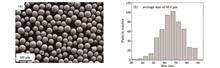
ObjectiveThe TC17 alloy has excellent mechanical strength, fracture toughness, and corrosion resistance and is primarily used in the manufacturing of aero engine disk components. Directed energy deposition (DED) can achieve specific location repairs of damaged parts and 3D printing of complex and large parts. DED of TC17 alloy has been successfully applied to such parts as integral blade disks. However, the low hardness and poor wear resistance of TC17 alloy make it susceptible to fatigue fracture under the harsh use environment of aero engines, which limits its application in the aerospace field. At present, the problems of poor bonding strength, introduction of new defects, and inability to meet various performance requirements in the spraying of hard coatings on titanium alloy surfaces present potential risks and limitations in aerospace applications. Optimized heat treatment has unique advantages in solving these problems. Optimized heat treatment can adjust material properties by adjusting the microstructure. Several studies have been conducted on improving the tensile properties of TC17 by optimizing the heat treatment process, but further research is needed on whether optimized heat treatments can improve the wear resistance of deposited TC17 alloy. Therefore, in this study, the effects of annealing, post-annealing solid solution, and post-annealing solid solution aging treatments on the microstructure, hardness, and tribological properties of deposited TC17 alloy are investigated. The evolution of the structure during heat treatment and the comprehensive wear behavior under 20 N dry sliding wear are analyzed. The results provide a reference for optimizing the tribological properties and heat treatment process of TC17 alloy.MethodsThe experimental material is TC17 spherical powder, with an average particle size of 66.6 μm (Fig. 1). The experiment uses the semiconductor laser to generate lasers, and the robot, equipped with coaxial powder feeding, deposits the TC17 powder on the polished TC4 substrate in the argon environment (Fig. 2). The process parameters are optimized: laser power of 1600 W, scanning speed of 10 mm/s, powder feeding rate of 11 g/min, overlap rate of 45%, and center protection gas flow rate of 11 L/min. A TC17 alloy sample (size of 75 mm×35 mm×12 mm) is obtained using an N-type scanning path. Samples are taken along the direction of laser deposition, with a sample size of 6 mm×6 mm×6 mm. The TC17 deposition samples are subjected to pre-annealing, annealing solid solution treatment, and annealing solid solution aging treatment (Fig. 3), and the microstructure and wear properties of the TC17 deposition and heat-treated samples are characterized by the X-ray diffraction (XRD), energy-dispersive X-ray spectroscope (EDS), scanning electron microscope (SEM), hardness tester, and pin-disk-type friction wear testing machine.Results and DiscussionsThe experimental results indicate that the deposited TC17 alloy consists of α and β phases, displaying a basketweave structure (Fig. 6). After annealing at 840 ℃, some of the fine α phase dissolves because of the high temperature. After solid solution treatment at 800 ℃, the primary α phase (αP) in the grain interior gradually flattens. During the annealing and post-annealing solid solution treatment stages (Fig. 7), affected by the diffusion rates of different elements, the grain boundary α phase (αGB) is divided into continuous αGB and discontinuous αGB. A phase-free zone (PFZ) appears around the continuous αGB because of the insufficient concentration of α stabilizing elements at the low-angle grain boundary. After aging at 580 ℃ based on the post-annealing solution treatment, a large amount of fine needle-like secondary α phase (αS) precipitates, and the PFZ disappears. When the temperature rises to 630 ℃, some of the ultrafine αS redissolves in the β matrix. After aging at 680 ℃, PFZ reappears with only partial coarsening αS interspersed between αP (Fig. 9). The αS precipitates inside the β grains, and the randomness of orientation makes the size and quantity of αS very sensitive to changes in aging temperature. After solution treatment, the average microhardness reaches 425.45 HV, which is higher than the hardness in the as-deposited state (Fig. 12). This is attributed to the precipitation and growth of αP, which increase the volume fraction of the phase, thereby improving the microhardness. After aging treatment, the hardness is further increased, reaching its highest value (~486.93 HV) after aging at 580 ℃. This is caused by the large amount of αS precipitation, which achieves the strongest dispersion-strengthening effect. The wear test results show that the wear properties of the heat treatment state are superior to those of the deposition state (Fig. 13). Table 3 shows the maximum wear widths and depths in different states. The tribological properties are the best after aging at 580 ℃, which is attributed to the significant increase in hardness and a large number of secondary phases inhibiting dislocation movement and crack expansion. After heat treatment, a variety of wear mechanisms coexist, and the wear rate and wear morphology depend on the changes in the microstructure and oxide layer.ConclusionsA TC17 sample is prepared by DED and then heat-treated. The changes in phase composition, microstructure, microhardness, and tribological properties during heat treatment are studied. The results show that the main microstructure evolution of TC17 alloy during heat treatment includes the growth and coarsening of αP; the continuous and discontinuous growth of αGB, where the width of PFZ is positively related to the continuous growth of αGB; and the precipitation and growth of αS, where, as the aging temperature increases, some αS dissolves and some grows to have a clear phase boundary with the β phase. The hardness after heat treatment is higher than that of the deposited state. In the solid solution stage after annealing, the hardness increases with the increase in α phase volume fraction. After further aging, the precipitation of αS achieves dispersion strengthening, and the strengthening effect weakens with the dissolution of αS. The hardening effect is higher at 580 ℃, and the hardness is increased by 20.1% compared with that of deposition state. The tribological performance after heat treatment is better than that in the deposition state. The increase in hardness, secondary phase precipitation, and hard oxide formation are the main reasons for the improvement of the tribological properties. Optimal wear resistance is achieved in the heat treatment systems of 840 ℃/1 h, air cooling+800 ℃/4 h, water quenching +580 ℃/8 h, and air cooling, with a friction coefficient (wear rate) of 0.422 (0.0451 mg/m).
Jun. 25, 2024Vol. 51 Issue 12 1202301 (2024)
Yangyang Wang, Mingyan Sun, Jie Chen, Yu Qin, Xianfeng Shen, Guowei Wang, and Shuke Huang
ObjectiveCompared with traditional manufacturing methods, selective laser melting (SLM) can form complex components. As 316 L stainless steel has excellent mechanical properties, several studies on additive manufacturing of 316L stainless steel have been conducted. However, current research on the impact toughness of 316L prepared by SLM based on the heat treatment temperature is insufficient, and the effect on anisotropy has not been reported. Therefore, in this study, we use the SLM method to prepare 316L impact components with different forming orientations and compare the impact toughness and anisotropy of the SLM-formed 316L stainless steel before and after heat treatment at different temperatures. The study provides technical ideas for regulating the microstructure and properties of 316 L stainless steel parts prepared by SLM.MethodsWe use 316 L stainless steel spherical powder. The selected process parameters are as follows: laser power of 280 W, scanning speed of 1150 mm/s, layer thickness of 30 μm, and scanning spacing of 0.1 mm. Impact specimens and micro-characterization specimens are prepared in an SLM equipment. Three impact specimens, namely XZ-X, XY-Z, and XY-X, are prepared according to different printing and notch orientations (Fig.2). They are heated to 1050 ℃ and 1100 ℃ in the vacuum furnace and held for 1 h after air cooling. Three groups of comparison samples with different states are obtained, namely the SLM state, heat treatment state at 1050 ℃, and heat treatment state at 1100 ℃. Finally, the prepared impact samples are subjected to the Charpy impact test at room temperature and characterized by X-ray diffractometer (XRD), scanning electron microscope (SEM), electron back-scattered diffraction (EBSD),and transmission electron microscope (TEM).Results and DiscussionsThe impact toughness of 316 L with different states and orientations shows an obvious trend. For different states, the impact toughness of SLM samples is the highest, followed by that of the heat treated sample at 1100 ℃, and that of the heat treated sample at 1050 ℃ is the lowest. For different orientations, the impact toughness of the XY-Z sample in the SLM state is the best, but it has the worst impact toughness after heat treatment (Fig.4). The phase composition characterized using XRD is found to be the single austenite phase (Fig.3). Using SEM and TEM to characterize the microstructure, it is found that 316L in the SLM state is composed of many fine crystals and cellular subgrains. After the heat treatment, recrystallization occurs, fine crystals transform into coarse grains, and subgrain boundaries gradually disappear. This phenomenon becomes more evident as the heat treatment temperature increases (Fig.7). Simultaneously, oxides rich in Si and Mn are observed in the SLM state (Fig.8). The size of the oxides increases significantly after heat treatment but does not increase after the heat treatment temperature reaches 1100 °C (Fig.9). EBSD characterization reveals that the grain size and proportion of large-angle grain boundaries increase after heat treatment, which becomes more evident as the heat treatment temperature increases (Fig.6 and Fig.10). Therefore, the effects of heat treatment on impact toughness and anisotropy are analyzed. Impact toughness is affected by oxide content, grain size, and large angle grain boundaries. Among these effects, the size of the oxide inclusions is dominant. The coarsening of the oxide after heat treatment significantly worsens the impact toughness. Although the increase in grain size and large-angle grain boundaries can improve the impact toughness, the effect on impact toughness is less than that of the oxide coarsening. It is believed that anisotropy is affected by the multi-layer structure and grain texture. The anisotropy of the SLM state is dominated by the multilayer structure, and the notch cracks of the XZ-X and XY-X samples expand between layers and are not hindered by the print layer. The notch cracks of the XY-Z samples expand perpendicular to the layer and are hindered layer by layer, releasing more energy when the impact is exerted (Fig.11). After heat treatment, the multilayer structure is destroyed, and the grain orientation of the XY plane is <110> (Fig.12), which is not conductive for increasing the impact toughness; therefore, the impact energy released by the XY-Z sample is lower.ConclusionsThe SLM sample exhibits the highest impact toughness, which decreases after heat treatment owing to an increase in inclusions. As the heat treatment temperature increases, the grain size and large-angle grain boundaries also increase, along with the impact toughness. The XY-Z sample in the SLM state has many impact obstacles and exhibits good toughness. After heat treatment, the obstacles are weakened, and the texture dominates. The <110> crystal orientation is not conducive to impact performance, and the toughness of the XY-Z sample decreases.
Jun. 25, 2024Vol. 51 Issue 12 1202302 (2024)
Ao Zhang, Wangping Wu, Peng Jiang, Zhizhi Wang, Haijun Pan, and Yi Zhang
ObjectiveLaser powder bed fusion (L-PBF) is a representative technology in metal/alloy additive manufacturing. It utilizes a laser as the heat source with a small beam size, enabling the production of fine and intricate parts. During L-PBF additive manufacturing of complex structure parts, the forming direction is variable which increases the complexity of heat transfer and solidification. As a result, the thermal efficiency differs among different forming directions, which can impact the performance of the printed parts. However, the current research on the influence of forming direction on the microstructure and properties of L-PBF 316L stainless steel is not sufficiently systematic. Therefore, it is further necessary to deeply investigate the influence of formation direction. We investigated the correlation between the forming direction and the microstructure and properties of L-PBF 316L stainless steel and explored the variations in mechanical properties to provide valuable insights for the development and applications of L-PBF 316L stainless steel.MethodsFirst, the 316L stainless steel parts were fabricated using L-PBF from two different forming directions of 0° and 60°. The microstructure and mechanical properties of the parts were investigated through metallographic and tensile tests. The phases of the 316L stainless steel powder and as-printed samples were determined using X-ray diffraction (XRD). The grain orientation distributions, grain sizes, and grain boundary angles of these samples at different deformation strains were characterized using electron backscattered diffraction (EBSD) and scanning electron microscope (SEM).Results and DiscussionsThe results show that some porosity defects occur in the L-PBF 316L stainless steel (Fig.5). During the printing process, the rapid cooling rate leads to the retention of the α-Fe ferrite phase (Fig.6). Tensile testing shows that the samples printed from the forming direction of 60° exhibit higher tensile strength than those from the forming direction of 0°, while the samples printed from the forming direction of 0° demonstrate better elongation than those from the forming direction of 60° (Fig.7 and Table 3). In-situ tensile testing results indicate that there exist significant differences in grain boundary angles, phase contents, surface morphologies, grain orientations, and grain sizes among the L-PBF 316L stainless steel samples printed from different forming directions during the tensile deformation process. In both 0° and 60°, the samples exhibit predominantly high-angle grain boundaries before tensile deformation. However, as the deformation strains increase, the proportion (volume fraction) of low-angle grain boundaries gradually increases and finally surpasses that of high-angle grain boundaries (Fig.9). In terms of phase composition, the γ-Fe face-centered cubic (FCC) phase account for over 98% in the sample before deformation, but its proportion (volume fraction) decreases while the α-Fe body-centered cubic (BCC) phase increases with increasing deformation strains (Fig.10 and Table 5). In terms of surface morphology, the samples underwent dislocation slip and twinning during the tensile process. The sample built from the forming direction of 0° exhibits much more slip bands as well as a large amount of deformation twinning compared with the part printed from the forming direction of 60°, which improves the tensile properties of the parts (Fig.11). In terms of grain orientation, the samples manufactured using L-PBF exhibit anisotropy. For the sample built from the forming direction of 0°, the initial <101>∥Z1 grain orientation gradually transforms to <001>∥X1 and <111>∥X1 during the tensile process. In contrast, for the sample built from the forming direction of 60°, the initial <111>∥Z1 grain orientation gradually transforms to <111>∥X1 during tensile deformation. This difference in grain orientation is related to the formation of deformation twinning within the grains during tensile deformation, which induces grain orientation rotation (Fig.12). In terms of grain size, the L-PBF 316L stainless steel undergoes grain refinement with increasing deformation strain. The coarse columnar grains in the as-printed state are progressively fractured under external forces, leading to a reduction in grain size with increasing strain. The sample built from the forming direction of 0° exhibits a higher degree of grain refinement and smaller grain size than the sample printed from the forming direction of 60° (Fig.13).ConclusionsThe influence of two forming directions of 0° and 60° on the microstructure and mechanical properties of L-PBF 316L stainless steel was studied. The evolution of microstructure and grain orientation during tensile deformation of L-PBF 316L stainless steel was studied using in-situ tensile testing. There are some defects in the L-PBF 316L stainless steel, and a fish-scale-like melt pool occurred in the part printed from the forming direction of 60°. The sample built from the forming direction of 60° exhibits a high tensile strength, while the part printed from the forming direction of 0° shows good elongation and plasticity. During in-situ tensile deformation, the proportion of low-angle grain boundaries and the α-Fe-BCC phase content increase, the grain size decreases, and the slip bands appear within the grains. Compared with the sample built from the forming direction of 60°, these changes are much more significant in the part printed from the forming direction of 0°. In the forming direction of 0°, the initial <101>∥Z1 grain orientation gradually transforms to <001>∥X1 and <111>∥X1 during tensile deformation, while in the forming direction of 60°, the initial <111>∥Z1 grain orientation gradually transforms to <111>∥X1.
Jun. 25, 2024Vol. 51 Issue 12 1202303 (2024)
Shuai Zhang, Tongzheng Liu, Zhihong Xu, Xiaoguang Dai, Zhaohui Zhu, Ming Gao, and Shaofeng Guo
ObjectiveTo achieve carbon neutrality, lithium batteries, as a new generation of green energy products, are poised to enter the terawatt-hour (TW·h, equivalent to 1000 GW·h) era. Currently, mainstream manufacturers of state-of-the-art energy batteries have reached a production capacity of 200 pieces per minute (PPM), and there are plans to increase the production capacity of cylindrical batteries to 300 PPM. Consequently, extremely high-speed production lines present substantial challenges to the welding process. Therefore, the development of highly efficient and reliable battery-welding technologies and processes has become an urgent concern for the automobile manufacturing industry. Laser welding, with its small laser spot, high energy density, efficient welding, precise energy control, automation capabilities, and safety features, has been widely used in the field of new energy battery welding, including vehicle manufacturing. Recent research has primarily focused on enhancing the welding quality of aluminum alloys by optimizing laser welding process parameters and beam shaping. However, as the demand for higher welding efficiency in power battery welding increases, the scope for ensuring both welding quality and speed becomes constrained, making it increasingly challenging to identify suitable process parameters. Considering that lasers, as a new type of welding light source, exhibit characteristics distinct from those of the arc light sources generated by arc welding machines, research has primarily focused on laser power. The impact of laser light source characteristics on welding quality and efficiency, particularly the influence of laser beam quality, has received limited attention. To meet the demands of high-speed production lines for new energy power batteries, the effect of the beam quality from fiber lasers in aluminum alloy laser welding is systematically analyzed in this study based on the energy distribution characteristics within the laser welding process. The quantitative relationship between beam quality and welding stability, as well as welding efficiency, is also explored.MethodsAn industrial-grade 3-kW continuous fiber laser is used in the experiment. The laser employs a circular swing path for welding with a swing amplitude of 0.6 mm and spacing of 0.25 mm. The upper-layer material consists of a 1.5-mm-thick 3003 aluminum alloy plate, while the lower-layer material is a 3-mm-thick 3003 aluminum alloy plate.Results and DiscussionsWith a decrease in the laser beam quality factor (M2), the welding speed increases, corresponding to the same weld penetration (2.7 mm), and the complex process capability index (CPK) value of weld penetration also increases. When the M2 is reduced from 11.6 to 1.25, the welding speed increases by 5.5 times, and the CPK value of the weld penetration increases by 2.3 times, corresponding to the same weld penetration (2.7 mm) (Fig. 4). Analyzing the energy distribution of postlaser welding oscillations on the YOZ surface reveals that, as the M2 improves, there is a consistent downward trend in the maximum value of the laser energy density. In addition, the area between the two maximum values decreases. For instance, the maximum energy density at M2=1.18 is 1.4 times higher than that at M2=11.6 (Fig. 5). To gauge the influence of the laser energy density on the welding efficiency, a factor derived from the product of the maximum laser energy density and the difference in the maximum value of the energy density is introduced. Calculations demonstrate that, at M2=1.18, this influence factor for laser energy density welding efficiency is 5.2 times higher compared with that at M2=11.6 (Fig. 6). To facilitate the assessment of the area disparities between the maximum peak and intermediate minimum at both ends of the weld, the region between these points on the energy distribution map is defined as the laser energy occupied space line density. Remarkably, when M2 is 1.18, the laser energy occupied space line density is 10.7 times greater than that when M2 is 11.6 (Fig. 6).ConclusionsThe influence of the beam quality from fiber lasers on aluminum alloy welding is systematically analyzed by considering the energy distribution characteristics during the welding process. A quantitative relationship between beam quality and welding stability, as well as welding efficiency, is established. The improvement mechanism for the laser beam quality effect is as follows. When the M2 decreases while retaining the same penetration depth, the maximum value of the energy density increases, and the energy density between the edge of the weld bead and the middle interval also increases. The higher the energy absorption efficiency of the workpiece material, the higher the welding efficiency of the laser. The product of the maximum value of the laser energy density and the difference in the maximum value of the energy density is used as a factor influencing the laser energy density welding efficiency. The theoretical calculations show that, when M2 is 1.18, the influence factor of the laser energy density welding efficiency is 5.2 times higher than that when M2 is 11.6, which is basically consistent with the experimental results.
Jun. 25, 2024Vol. 51 Issue 12 1202101 (2024)
Yichen Li, Lei Wang, He Li, Yong Peng, Runhuan Cai, and Kehong Wang
ObjectiveLaser utilization as a heat source to connect nickel-based superalloys has been applied in aviation, aerospace, weapons manufacturing and other fields. Solidification behavior of the laser welding molten pool of nickel-based alloys, including the nucleation, growth, collision and movement of grains, and the diffusion, enrichment and segregation of alloying elements, directly affect nickel-based alloy laser weld performance. Therefore, in-depth research of the solidification behavior of the nickel-based alloy laser welding molten pool is of paramount significance, particularly for laser welding process optimization, welding defect formation control, and the improvement of laser weld mechanical properties.MethodsThe macroscopic heat and mass transfer coupling model alongside microstructure evolution is utilized to quantitatively simulate the macroscopic heat and mass transfer, and the microstructure evolution of a laser welded IN718 alloy. The fluid volume (VOF) method is used to simulate the molten pool morphology and temperature field distribution of the macroscopic heat transfer process, and the temperature field distribution replaces the solidification parameter variables relating to the phase field control equation and is brought into the phase field model for microstructure evolution process simulation.Results and DiscussionsThe simulated and experimental microstructures are shown in Fig.6, where it can be observed that all tissues are columnar crystal structures with a consistent morphology. As shown in Fig.7(a), the solidification velocity R and temperature gradient G at different positions were extracted in the macroscopic simulation results. The solidification velocity R gradually decreased from top to bottom with the molten pool boundary, and the temperature gradient G gradually increased. The cooling rate G·R showed a decreasing trend, the dendrite spacing gradually increased, and the results are shown in Fig.7(b). Compared with the Hunt and Kurz et al. numerical models, the phase field model calculated results are more accurate and close to the experimental results, showing consistent regularity, as shown in Fig.8. The distribution of Nb elements perpendicular to the growth direction of columnar crystals in the simulation results is shown in Fig.9 (b), this shows obvious periodic changes, and the change period is closely related to the phase morphology, because the IN718 solute partition coefficient is less than 1. Solute elements tend to be segregated and enriched at the dendrite gap position. In the simulation results, the mass fraction of Nb elements inside the solid-phase dendrite is significantly reduced, and the lowest mass fraction occurs at the columnar center owing to segregation caused by solute redistribution during solidification. The mass fraction of Nb element increased significantly at the liquid phase position of columnar crystal gap, and the mass fraction of Nb element in the position was relatively higher than that closer to the bottom of the columnar crystal. From Fig.10, the Laves phase enriched by the Nb element precipitated from the IN718 molten pool after solidification is distributed in the γ phase matrix in the shape of droplets. The Laves phase morphology and distribution are approximately consistent with the simulated distribution of Nb elements. The SEM results are shown in Fig.11(b), the EDS spot scan analysis is performed on the illustrated position, with the test results shown in Figs.11(a) and (c). The mass fraction of Nb element in the matrix γ is approximately 4.7%. The mass fraction of Nb element in the Laves phase is approximately 9.8%, and the Nb element mass fraction in Laves phase is significantly higher than that in matrix γ. This proves the accuracy and reliability of the simulation results.ConclusionsThe results demonstrate that the simulated microstructure grows in a columnar crystal structure. The solidification rate R of the molten pool gradually decreases from top to bottom, the temperature gradient G gradually increases, the cooling rate G*R decreases continuously, and the primary dendrite arm spacing increases with the decrease in cooling rate, from 4.52 to 7.12 μm, which is consistent with the experimental results. The mass fraction of Nb elements in the columnar crystal spacing increased significantly, and this mass fraction was relatively higher near the bottom of the columnar crystals in the liquid phase. The Nb elements are finally distributed in the shape of droplets and approximately consistent with the Laves phase in morphology and distribution, which is also consistent with the experimental results. The microstructure transformation process and elemental segregation behavior of IN718 in laser welding are examined, and the solidification theory of the laser welding molten pool of nickel-based alloys is enriched. Finally, this research provides a foundation for a numerical solution of the defect formation process for laser welding IN718 cracks and pores.
Jun. 25, 2024Vol. 51 Issue 12 1202102 (2024)
Yue Cui, Ruixing Wang, Te Ma, Wu Yuan, Hongwei Song, and Chenguang Huang
ObjectiveLaser technology is extensively used in various fields, including additive manufacturing, removal processing, and laser weaponry. This technology has the potential to revolutionize battlefield dynamics through defensive and offensive applications. Research on laser irradiation under high-speed airflow provides a theoretical basis for efficient damage strategies and the protection of aircraft, this is crucial for deploying military laser systems. However, conducting real-scale model tests for large-scale engineering structures is challenging due to equipment limitations and testing environments. Additionally, wind tunnel tests with real-scale models are prohibitively expensive and time-consuming, preventing extensive testing. Consequently, scaled-model tests are often relied upon for regularity studies. Therefore, establishing a similarity relationship in the thermomechanical responses between real and scaled models under laser irradiation and high-speed airflow is a practical approach. Significant efforts have been made to understand the similarity theory of laser-induced thermomechanical behavior under static air conditions. Nonetheless, due to the complex fluid-thermal-structural interactions in high-speed airflow, the similarity criteria for thermomechanical responses in an airflow environment significantly differ from those in static air. In this study, we propose new similarity criteria and scaling laws suitable for the thermomechanical responses of a metal plate subjected to high-speed airflow and laser irradiation.MethodsTo clarify the similarity relation of thermomechanical responses for metal plates under coupling conditions, the effects of the tangential airflow were equivalently converted to the structural force and thermal load boundary conditions using the approximate equivalence method, and the dimensionless governing equations of the coupling problem were established. Thus, combined with the analysis of dominant factors, the similarity criteria and scaling laws suitable for the thermomechanical responses of the metal plate under the combined action of a high-speed airflow and laser were determined. According to the similarity criteria, there is a contradiction in the similarity relationship between the thermal boundary condition and force boundary condition under the fluid-thermal-structural coupling effects, which cannot be satisfied simultaneously. Considering that the thermal stress induced by the temperature gradient is much greater than the mechanical stress due to the aerodynamic force under the combined action of high-speed airflow and laser irradiation, this study focused on the similarity of aerodynamic heat transfer, ignored that of the aerodynamic force, and established the corresponding scaling law. Then, a fluid-thermal-structural coupling numerical example of a metal plate irradiated by a high-power laser under tangential flow was conducted to verify the scaling law under different scale ratios and Mach numbers.Results and DiscussionsThe similarity criteria and scaling laws for the fluid-thermal-structural coupling analysis of the metal plate subjected to laser irradiation and high-speed airflow are presented in Tables 1 and 2, respectively. A numerical example of the fluid-thermal-structural coupling of a metal plate irradiated by a high-power laser under a tangential flow is conducted to verify the scaling law. The results show that under different scale ratios and Mach numbers, the predicted response errors between the scaled and original models are within 1%, which proves the reliability and accuracy of the scaling law. Simultaneously, with the increase in scale ratios or Mach numbers, the aerodynamic heat transfer effect is enhanced, making the thermal-mechanical response difference between the scaled model and real model more obvious when the aerodynamic similarity criteria are not considered.ConclusionsIn this study, similarity criteria and scaling laws suitable for the thermomechanical responses of a metal plate under the combined action of a high-speed airflow and laser are determined. Several numerical examples are conducted and compared to verify the proposed similarity criteria and scaling laws. The main conclusions are as follows: (1) Using the approximate equivalence method and analysis of dominant factors, the effects of the tangential airflow are equivalently converted to structural force and thermal load boundary conditions, and the similarity criteria and scaling laws are determined. Considering that the thermal stress induced by the temperature gradient is significantly greater than the mechanical stress caused by the aerodynamic force, this study focusses on the similarity of the aerodynamic heat transfer and ignores the similarity of the aerodynamic force. (2) A fluid-thermal-structural coupling numerical example of a metal plate irradiated by a high-power laser under tangential flow was conducted to verify the scaling laws under different scale ratios and Mach numbers. The results show that the predicted response errors between the scaled and original models are within 1%, which proves the reliability and accuracy of the scaling laws. (3) However, the scope of application of the proposed similarity criteria should be emphasized in the following aspects: the similarity criteria are applicable for calorically perfect gases. For hypersonic flows, complex chemical reactions occur at high temperatures, and the similarity criteria are no longer applicable. The similarity criteria are applicable for the plate flow condition. However, for the non-plate flow, such as the flow around a blunt-nosed bodies, the similarity criteria are no longer applicable. The similarity criteria are applicable to the thermal-mechanical responses of the metal structure before melting. When melting is involved, similarity criteria are no longer applicable.
Jun. 25, 2024Vol. 51 Issue 12 1202103 (2024)
Jinfang Dong, Fangyi Yang, Di Wu, Xiaoting Li, Da Zeng, Hongxing Huang, Hao Wu, Peng Zhang, Liangyin Jiang, and Peilei Zhang
ObjectiveWith the development of the new energy vehicle industry, laser welding has become increasingly popular in the manufacturing of power batteries because of its high welding speed, small heat-affected zones, and high degree of automation. However, as the laser involves high-energy beam, its interaction with materials is often intense. This can easily lead to defects, such as spatters and explosion points, thus compromising the quality of battery welding. In the field of power batteries, the adjustable ring-mode (ARM) laser has emerged as a high-speed low-spatter laser welding tool, gaining attention from both academia and industry. However, the spatter suppression mechanism of the ARM laser during high-speed welding remains unclear. This limitation hinders theoretical guidance and process optimization for industrial applications. Thus, in this study, the complete welding of an aluminum alloy roof is considered and how the core ring power ratio affects the penetration and width is analyzed. Moreover, how the ARM laser effectively curbs the metal spatter is elucidated by examining the dynamic behavior of the keyhole in the molten pool. Optical coherence tomography (OCT) measurement technology is used to monitor keyhole depth fluctuations in real time, providing a quantitative assessment of welding stability and identifying the optimal process window.MethodsA synchronous-sensing monitoring platform (Fig. 1) is established by integrating high-speed visual shooting with penetration detection. For the visual sensing component, a high-speed camera is utilized to capture sharp keyhole images of the molten pool. For penetration detection, the platform is merged with an OCT-based monitoring module to acquire real-time keyhole depth information during the welding process. Initially, the process window of the ARM laser welding is determined by conducting an orthogonal experiment, as shown in Fig. 3. The keyhole images under different parameters are obtained, and the changes in the keyhole depth are recorded. Comparisons of the keyhole opening and depth reveal the mechanism behind the spatter suppression during ARM laser welding. To identify the best low-spatter process window, keyhole volatility is introduced as a variable. The variance in the keyhole depth, measured by applying OCT in real time, is calculated. This variance is used to assess the depth fluctuations of the keyhole and, consequently, the stability of the welding process. The relationship between the welding process stability and the power ratios of inner ring laser to outer ring laser is then established by using a contour map, resulting in the identification of optimal process window parameters (Fig. 10).Results and DiscussionsThe spatter formation mechanism in the ARM laser high-speed (150 mm/s) welding is analyzed. The spatter formation process and suppression methods are elucidated, demonstrating that the ARM laser can indeed diminish the spatter occurrence rate by enlarging the keyhole opening. The effect of the power ratio of inner ring laser to outer ring laser on the keyhole stability is verified. First, a traditional orthogonal experiment is conducted to determine the process window for melting width when the inner ring laser power ranges from 600 W to 1300 W and the outer ring laser power ranges from 800 W to 1800 W. The process window for the penetration is determined for an inner ring laser power of 500?1150 W and outer ring laser power of 800?1800 W. Subsequently, the optical coherence scanning technology is employed to acquire the keyhole depth information. This information enables a qualitative evaluation of the welding process stability, facilitating the process optimization of the ARM laser welding. The findings suggest that a higher outer ring laser power is better for achieving a suitable penetration. A higher outer laser ring power stabilizes molten pool fluctuations and enlarges the keyhole opening.ConclusionsThis study presents a process optimization scheme combined with real-time monitoring of the laser welding depth. The theory that spatter is mainly caused by keyhole collapse is verified. The laser welding process is further optimized based on the standard deviation of keyhole depth fluctuations. The final process window that satisfies both the traditional process window and keyhole fluctuation stability analysis window is identified: the core laser power ranges from 800 W to 1000 W, ring laser power is between 1200 W and 1600 W, and welding speed is set at 150 mm/s. The optimal power ratio of inner ring laser to outer ring laser for welding aluminum alloys typically lies between 1∶2 and 1∶3. Within this range, the keyhole achieves maximum stability and the defect occurrence rate is the smallest.
Jun. 25, 2024Vol. 51 Issue 12 1202104 (2024)
Yonghong Liu, Chuang Cai, Jia Xie, Bingbing Zhang, Jie Yu, and Jiasen Huang
ObjectiveThe use of low-density lightweight materials, such as aluminum alloys, instead of traditional steel, titanium, and other materials to form a dissimilar material composite structure is an important way to achieve a light weight. Because of the different physical and chemical properties of aluminum alloys and steel, it is difficult to join aluminum and steel by laser welding-brazing. Brittle intermetallic compounds (IMCs) in the interface layer are easily produced owing to the small solid solubility between iron and aluminum. In this research, a rotating laser is applied to improve the temperature distribution and optimize the interface reaction. Based on the analysis of the morphology, type, and thickness of the interface layer of the aluminum/steel laser welding-brazing joint under different rotating parameters, the mechanical properties of the aluminum/steel welded joint are studied by a tensile test, and the fracture morphology and fracture mode of the joint are also investigated.MethodsThe test materials are a 304 stainless-steel plate with a size of 100.0 mm×80.0 mm×0.9 mm and a 6061-T6 aluminum alloy sheet with a size of 100.0 mm×80.0 mm×1.2 mm. AlSi12 is used as filler wire. A fiber laser is used as the heat source. High-purity argon (volume fraction of 99.99%) with a gas flow rate of 25 L/min is used as the protective gas. After welding, the cross-sectional morphology of the weld is observed by using a metallographic microscope. A scanning electron microscope (SEM) is used to analyze the morphology and thickness of the IMC layer. The chemical composition of the interface layer is detected using an energy-dispersive X-ray spectroscope (EDS) system integrated with the SEM. The mechanical performance of the joint is represented by the line load. The fracture morphology is observed using the secondary electron detector of the SEM.Results and DiscussionsAfter the addition of the rotating laser, the thickness of IMCs composed of θ-(Fe, Ni)(Al, Si)3 and τ5-(Fe, Ni)1.8Al7.2Si is significantly reduced, and the uniformity of the IMC layers is improved. The line load of the joint without a rotating laser is 215.9 N/mm. The joint with a rotation diameter of 2 mm has the largest line load of 289.1 N/mm, which is 33.9% higher than that without rotation. Compared with nonrotating-laser joints, the joint line load increases because of the thinning of the intermetallic layer and the reduction of the complexity of the IMC. At a rotation diameter of 2 mm and frequency of 30 Hz, a fracture occurs at the weld. Under these parameters, the IMC thickness of the joint is uniform and only composed of the τ5-(Fe, Ni)1.8Al7.2Si phase. Compared with the θ-(Fe, Ni)(Al, Si)3/τ5-(Fe, Ni)1.8Al7.2Si interface, a single τ5-(Fe, Ni)1.8Al7.2Si/steel interface achieves relatively low interface crystal plane mismatch and better bonding performance, thereby improving the tensile performance of the joint. In the EDS results in Table 4, α-Al and Al-Si eutectic on the fracture can be observed. Additionally, many dents are formed on the fracture, and the fracture mode is ductile fracture.ConclusionsCompared with the rotating frequency, the rotating diameter has a greater influence on the wetting width of the joint. To obtain a well-formed rotating laser welding-brazing aluminum/steel joint, the welding process parameters should be optimized with a laser rotating diameter of 2 mm. When the laser is not rotating, two layers of IMCs with a thickness of approximately 8.45 μm are formed at the interface. After the rotating laser is applied, the thickness of the intermediate layer is reduced, and the variety is decreased. The rotating laser reduces the welding peak temperature and inhibits the formation of brittle IMCs. At a laser rotation diameter of 2 mm and frequency of 30 Hz, the linear load reaches a maximum value of 289.1 N/mm, which is approximately 33.9% higher than that without the rotating laser. The fracture position of the joint changes from the interface layer without the rotating laser to the weld.
Jun. 25, 2024Vol. 51 Issue 12 1202105 (2024)
Chenqian Yu, Gang Ren, Yingjie Huang, and Ming Gao
ObjectiveLaser welding has the characteristics of a high energy density, low heat input, and high welding efficiency; however, conventional laser welding has a small focused spot and high requirements for the welding assembly gap. To solve this problem, scholars have developed laser wire filling welding technology. Based on this, some scholars have developed laser hot wire welding technology, which can effectively improve the absorptivity of the welding wire by preheating the welding wire in advance, reduce the requirements for laser power, and improve the welding speed; however, there are still problems such as high requirements for the alignment of the laser focus and the tip of the welding wire, and an uneven weld height. In this study, the process characteristics of Q235 steel by scanning laser hot wire welding are systematically studied, and the mechanism of the influence of the scanning laser on the solidification process of weld metal is clarified, which provides technical guidance for expanding the industrial application of laser welding.MethodsThe base material used in this study is the Q235 steel plate. The size is 50 mm×120 mm×2 mm, and the structure is massive ferrite at normal temperature. The flat surfacing welding method is used in the research on the weld surface and section forming. The docking method is adopted in the study of the microstructure and properties of welded joints. According to the previous research and accumulation of this research group, the fixed wire feeding method is front wire feeding, the tilt angle of the welding torch is 45°, and the laser focus is located on the surface of the plate, that is, the defocus quantity is 0 mm. In the welding process, the shielding gas is argon with purity (volume fraction) greater than 99.99%. The gas pipe angle is 60° and the gas flow rate is approximately 20 L/min. In the butt welding experiment, the fixed laser power is 1.8 kW, the welding speed is 1.0 m/min, the preheating current of laser cold wire welding is 0 A, the preheating current of laser hot wire welding is 100 A, the scanning amplitude ranges from 0.6 mm to 1.0 mm, and the scanning frequency ranges from 100 Hz to 200 Hz.Results and DiscussionsUnder different scanning parameters, the distribution of the laser energy is different, which affects the temperature field distribution of the weld pool, and then affects the macro forming, microstructure, and properties of the weld. Compared with that in non-scanning laser hot wire welding, the weld forming in scanning laser hot wire welding is smoother and straighter, and the splash is less (Fig. 5). The weld structure in non-scanning laser hot wire welding is dominated by thick side lath ferrite. Because the scanning laser enhances the flow of the molten pool through the stirring effect and breaks the coarse columnar crystals, the weld structure in scanning laser hot wire welding is dominated by fine crystalline ferrite and acicular ferrite with finer grains (Fig. 7). The tensile strength (578.8 MPa) of the scanning laser hot wire welded joint is basically the same as that (574.7 MPa) of the non- scanning laser hot wire welded joint, but the elongation is increased from 8.4% to 13.1% (Table 3). The dimple size of the tensile fracture surface of the scanning laser hot wire welded joint is more uniform, and the dimple size difference between the laser hot wire welded joint and the laser cold wire welded joint is larger; moreover, there is obvious inclusion precipitation at the bottom of the dimple, indicating that the scanning laser improves the homogeneity of the weld structure (Fig. 10). Simultaneously, the scanning laser improves the gap tolerance during butt welding. In the butt welding experiment of the Q235 steel plate with a thickness of 2 mm, the scanning laser hot wire welding ensures good weld formation without defects when the gap is 1.3 mm (Fig. 12).ConclusionsIn the experiment of scanning laser hot wire welding, by optimizing the process parameters, when the scanning diameter is 0.4?1.0 mm and the scanning frequency is 50?200 Hz, the welds obtained are well formed, smooth, no defects and nearly no splash, which proves that the scanning laser has a good improvement effect on the weld formation. Simultaneously, the scanning laser improves the gap tolerance of laser hot wire welding, which is conducive to achieve stable welding when the gap is uneven and obtain a weld with good fusion with the base metal side wall and no surface collapse. At the microstructure level, the stirring effect of the scanning laser on the weld pool can promote the flow of the weld pool and refine the grain. In terms of mechanical properties, compared with that in non- scanning laser hot wire welding, when the tensile strength is basically unchanged, the fracture elongation increases to 13.1% in scanning laser hot wire welding, indicating that the addition of the scanning laser can effectively improve the toughness of the weld, which is also proved by the deeper dimples in the electron microscope image of the fracture. The hardness of the fusion zone in the laser hot wire welding is the highest, followed by that of the heat affected zone, whereas the hardness of the base metal is the lowest. The hardness of the fusion zone in the scanning laser hot wire welding is lower than that in the non- scanning laser hot wire welding, mainly because the fusion zone in the non- scanning laser hot wire welding is easy to produce segregation, and the generated inclusions increase the microhardness.
Jun. 25, 2024Vol. 51 Issue 12 1202106 (2024)
Yafeng Zheng, Hechao Wang, Haojie Zhang, Qunli Zhang, Liang Wang, Huaxia Zhang, Rangda Wu, and Jianhua Yao
ObjectiveCompared with laser welding and arc welding, laser-arc hybrid welding not only inherits the advantages of laser welding and arc welding but also makes up for respective shortcomings. Thus, it is an advanced welding process method with great application prospects. With the continuous development of laser technologies, laser power has exceeded 10 kW or even higher. Therefore, in order to make the development of lasers well meet the need of actual industrial production, the basic theoretical research on high-power laser-arc hybrid welding has been a hot spot in the academic community in recent years. Researchers have carried out a lot of research on the interaction mechanism between laser and arc. However, the laser power involved was mostly below 5 kW. There are few reports on the mechanism regarding the effect of a high-power (higher than 5 kW) laser on the droplet transfer in laser-arc hybrid welding. Therefore, in this study, a high-power (7.5 kW) laser is introduced into the different modes of arc [standard metal active-gas(MAG), cold metal transfer (CMT), and pulsed arc] welding process, and its effects on droplet transition, weld forming and welding efficiency are compared and studied by using high-speed camera, optical microscope, etc.MethodsIn this study, a high-power laser-arc hybrid welding platform was built, which mainly consisted of a continuous fiber laser, a welding system, a manipulator arm, and a high-speed camera system. The high-power laser-arc hybrid welding experiments were carried out on 10 mm thick Q345 steel, and the laser used in the test was a fiber laser (maximum output power of 12 kW), with an output laser wavelength of (1080±10) nm and a focused spot diameter of 0.2 mm. Before the welding test, an angle grinder was first used to grind the surface to be welded, and then the ground surface was cleaned with alcohol. The arc-guided laser-arc welding was chosen for obtaining a stable droplet transition process. In order to further understand the influence of a high-power laser on droplet transition in different modes of arc welding, the laser was coupled with three different arc modes (standard MAG, CMT and pulsed arc). The welding shielding gas used in the welding process was the Ar and CO2 mixture with a flow rate of 20 L/min. During the welding process, a high-speed camera was used to track and monitor the droplet transition behavior with a frame rate of 10000 frame/s. In order to obtain a clear droplet transition image, an infrared filter was added to the camera lens before the experiment began. Image pro plus software was used to process the pictures taken by the high-speed camera, and the droplet transition mode and the number of droplet transitions within 500 ms under each parameter were counted, so as to calculate the droplet transition frequency within 1 s. After welding, the forward and cross-sectional morphologies of the weld were observed by optical microscope.Results and DiscussionsThe high-power laser has a significant effect on the droplet transition mode of arc welding in different arc modes. During standard MAG welding, the high-power laser attracts and compresses the arc, resulting in a significant reduction in arc length. Meanwhile, metal vapor and plasma ejected from the keyhole reduce the droplet transition frequency (Figs. 6 and 7). In the case of CMT welding, the high-power laser extends the single short-circuit transition period, and the resulting molten pool oscillation reduces the stability of the short-circuit transition (Fig. 8). Regarding the pulsed arc welding process, the high-power laser increases the melting rate of the welding wire. In the meantime, the droplet transition mode changes from the droplet transition to the jet transition, and the droplet transition frequency is significantly increased. The air flow at the key hole hinders the droplet transition, so that the droplet transits to the side of the molten pool (Figs. 11 and 12). Compared with that during arc welding, the weld melting width increases during laser-standard MAG and laser-pulsed arc hybrid welding, while no obvious change in weld width is observed in the case of laser-CMT hybrid welding. The residual height of welds in laser-standard MAG and laser-CMT hybrid welding decreases significantly, while the residual height of welds in laser-pulsed arc hybrid welding increases slightly. This is attributed to different degrees of influence of the laser on the droplet diameter and transition frequency in three different modes of arc welding. Furthermore, the melting energy increment value (ψ) of laser-arc interaction varies under different hybrid welding conditions, among which laser-pulse arc welding has the highest ψ value (36%), followed by laser- standard MAG welding (19%), while laser-CMT welding has the smallest ψ value (-12%).ConclusionsIn this study, the effects of laser (7.5 kW power) on droplet transition and weld formation in different modes of arc welding were investigated. The results reveal that the addition of laser has a significant influence on the droplet transition in standard MAG, CMT and pulsed arc welding processes. During standard MAG welding, the high-power laser attracts and compresses the arc, resulting in a significant reduction in arc length, and the metal vapor and plasma ejected from the keyhole reduce the droplet transition frequency. In the CMT welding process, the laser extends the single short-circuit transition cycle, and the melt pool oscillation caused by the high-power laser reduces the stability of the short-circuit transition. Regarding the pulsed arc welding process, the addition of a high-power laser increases the melting rate of welding wires. The droplet transition mode changes from the droplet transition to the jet transition, and the droplet transition frequency increases. Meanwhile, the air flow at the key hole hinders the droplet transition, so that the droplet transits to the side of the molten pool. Compared with arc welding, the weld melting width increases during laser-standard MAG and laser-pulsed arc welding, while no obvious changes in weld width are observed in the case of laser-CMT hybrid welding. The residual height of the welds in laser-standard MAG and laser-CMT hybrid welding decreases significantly, while the residual height of welds in laser-pulsed arc hybrid welding increases slightly. The melting energy increment values of the interaction between laser and arc under three arc modes are: laser-pulsed arc hybrid welding (36%), laser-standard MAG hybrid welding (19%), and laser-CMT hybrid welding (-12%).
Jun. 25, 2024Vol. 51 Issue 12 1202107 (2024)
Feng Tang, Deng Pan, Fei Yu, Kunjing Huang, Yanlei Hu, Dong Wu, and Jiawen Li
A spatial light modulator (SLM) is a diffractive optical device that modulates the wavefront of a light wave. It can modulate a light beam into a predesigned spatial light field. SLMs can be categorized into phase and amplitude types depending on the modulation physical quantities. The most commonly used devices are liquid-crystal spatial light modulators (LC-SLMs) and digital micromirror devices (DMDs). In recent years, researchers have used SLMs to modulate various forms of light fields. Based on the modulated light fields, they have efficiently processed and fabricated micro-nano structures with specific shapes, thereby improving the efficiency and processing accuracy of femtosecond laser TPP.Herein, the main research achievements of SLM-assisted TPP technology in the past decade are summarized, including holographic processing based on iterative algorithms, holographic processing based on structured light fields, interferometric holographic processing, and spatiotemporal focusing. The advantages and disadvantages of various methods are analyzed, and their applications in various fields are discussed. Finally, existing issues associated with the processing methods are discussed, and future endeavors are proposed.Another commonly used modulated light field is the structured light field, which enables the effective modulation of the incident laser light via the simulation of existing optical devices. Researchers have simulated optical devices such as cone lenses, Fresnel lenses, and helical phase plates to modulate beams into long-focus beams (Fig. 4) and higher-order Bessel beams (Fig. 5), toroidal Fresnel beams (Fig. 6), Airy beams (Fig. 7), and Mathieu beams (Fig. 8). Various micro-nano structures, including micropillars, hollow microtubes, and micro-cages with high aspect ratios, have been fabricated.Meanwhile, some researchers have adopted optical interference to generate more complex light fields. Specifically, multibeam laser interference was simulated by loading computational holograms on an SLM to form periodic or custom-shaped light field distributions, and functional structures such as helical structures or chiral microstructures were prepared in a single exposure (Figs. 9 and 10).Finally, femtosecond laser TPP has yielded impressive results in micro-nano structure processing. However, further improvements are required to efficiently prepare cross-scale (nano-micron-centimeter) structures. Furthermore, conventional femtosecond lasers result in elliptical asymmetric focal cross-sections owing to the inequality between the beam focal radius and Rayleigh length. This renders it challenging to achieve a spherical focal point with isotropic resolution in 3D space. Hence, researchers have combined SLMs with spatiotemporal focusing to efficiently process cross-scale micro-nano structures with high precision (Fig. 11).Although femtosecond laser TPP based on SLMs has achieved significant breakthroughs, some of its aspects can be further improved: 1) The range of materials suitable for femtosecond laser TPP can be further broadened to accommodate other fabrication processes to further expand the functionality of micro-nano structures. 2) To satisfy the requirements of practical applications, the efficiency of SLM-assisted TPP must be further improved. 3) The algorithms for the iterative generation of high-quality 3D light fields should be further investigated. 4) The generation and modulation of novel structured light fields should be further developed.SignificanceFemtosecond laser two-photon polymerization (TPP) technology enables the direct three-dimensional (3D) printing of micro-nano structures with submicron precision. This technology has broad application prospects in many fields. Conventional femtosecond laser TPP uses a point-by-point scanning strategy to shape 3D structures. Specifically, it requires the focused spot to traverse the 3D spatial coordinates of the structure to be processed, thus rendering the efficient fabrication of 3D devices challenging. Consequently, the application of this technology is limited in various fields. Optical modulation technology can be applied to modulate incident light into the target light field, which significantly improves the processing efficiency and reduces the processing time. Thus, it can serve as a basis for high-throughput large-area manufacturing.ProgressLight field modulation can improve processing efficiency and accuracy. Achieving high-quality light field modulation is a priority for many researchers. Using various hologram iterative algorithms, such as the Gerchberg-Saxton (GS) and weighted Gerchberg-Saxton (GSW) algorithms, researchers have successfully achieved the rapid machining of repetitive structures by modulating the incident laser into a multifocal shape (Fig. 1). Furthermore, researchers have realized the flexible processing of multiple foci by dynamically loading holograms combined with the movement of the carrier table (Fig. 2). Additionally, the efficiency of TPP has been improved by modulating the light field into a patterned or 3D light field and then enhancing the uniformity of the light field, thus enabling complex micro-nano structures to be processed in a single exposure (Fig. 3).Conclusions and ProspectsIn this paper, domestic and international studies pertaining to SLMs in femtosecond laser TPP are reviewed. In particular, holographic processing based on iterative algorithms, holographic processing based on structured light fields, interferometric holographic processing, and spatiotemporal focusing high-efficiency processing are discussed. The implementation methods and development process of femtosecond laser TPP for efficient processing are discussed, and the advantages and disadvantages of each method are summarized.
May. 20, 2024Vol. 51 Issue 12 1202401 (2024)
Hantong Zhao, Sihua Su, Chen Li, Mingxia Zhou, Zezheng Zhang, Chen Zhang, Qifeng Ruan, and Qinghai Song
Progress The rapid evolution of information technology imposes continuous demands on information transfer speed, the energy consumption of devices, and anti-interference performance. In this context, photons, which serve as information carrier, exhibit greater capability in terms of information processing compared with electrons. Photonic crystals, which are recognized as quintessential structures for manipulating photons, have garnered substantial research interest. The periodic arrangement of materials with varying refractive indices in photonic crystals results in advanced optical modes, including photonic band gaps and slow light modes (Fig.1). The conceptualization of photonic crystals has significantly advanced investigations into micro/nano optics and optical devices, thus promoting the development of optical communication, information displays, and integrated photonics. Optical components fabricated using one- and two-dimensional photonic crystals have been investigated comprehensively and applied extensively. However, the effective utilization of 3D photonic crystals, which are characterized by periodic structures in all three orthogonal directions, remains hindered by limitations in micro/nano manufacturing technology. The creation of 3D photonic crystals with attributes such as high precision, minimal random defects, high yield, and controllable 3D profiles presents several challenges. To propel the progress and practical application of photonic crystals, comprehensive investigations into 3D micro/nano processing technology are warranted.Diverse techniques are employed to fabricate photonic crystals, among which mask-projection lithography, nanoimprint lithography, and electron/ion-beam lithography are the predominant methods used for creating planar structures. Complex structures achieved via these methods typically involve the layered stacking of planar components, which presents challenges in realizing arbitrary 3D structures. Self-assembly is typically conducted to form densely packed particles, which yields large-area samples with random defects, thus rendering it difficult to control the overall 3D contour of the structure. As an effective micro/nano manufacturing technology for fabricating arbitrary 3D structures, TPL is the preferred method for manufacturing 3D photonic crystals (Fig.2). In this regard, continuous efforts are directed toward advancing the resolution (Fig.3), accelerating the printing speed, and diversifying the material library (Fig.4) for the TPL-based production of 3D photonic crystals. The resulting 3D photonic crystals demonstrate outstanding performance in structural color displays (Fig.5) and many other optical applications (Fig.6).Conclusions and Prospects The synergy between research pertaining to 3D photonic crystals and advancements in TPL technology is evident. Serving as exemplary 3D structures, photonic crystals function as standardized printing models that facilitate the meticulous evaluation of TPL performance. Concurrently, the evolution of TPL technology streamlines the preparation and experimental investigation of 3D photonic crystals. By leveraging their unique light manipulation capabilities, 3D photonic crystals offer significant potential in the optical domain. Augmenting TPL technology with a diverse range of functional materials will expand the application scope of photonic crystals. The trajectory of future research entails harnessing micro/nano processing technologies such as TPL to fabricate a myriad of photonic crystals and other optical components on a monolithic chip, thereby facilitating the development of high-performance integrated optical circuits. Beyond optics, 3D photonic crystals can be applied to energy, biomedicine, and other fields. From enhancing the efficiency of solar cells to crafting 3D micro-scaffolds for guiding cell growth, their potential applications are expansive. The ongoing research pertaining to TPL technology and 3D photonic crystals can create new possibilities for scientific research activities that benefit daily life.SignificanceInvestigations pertaining to two-photon polymerization lithography (TPL) and photonic crystals are mutually reinforcing. This review first outlines the concept and typical structures of three-dimensional (3D) photonic crystals, as well as the principles and characteristics of TPL technology. Subsequently, research progress pertaining to the utilization of TPL for printing 3D photonic crystals is introduced, with emphasis on aspects such as resolution, printing speed, and the extension of material library. Additionally, the potential applications of 3D photonic crystals in the field of optics are highlighted. Finally, the existing challenges in the TPL printing of 3D photonic crystals are discussed, and the prospective future research directions are presented.
May. 29, 2024Vol. 51 Issue 12 1202402 (2024)
Lijia Xu, Qingsong Wang, Xiaofang Fu, Qi Zhang, Qiong He, Zeyu Zhao, and Xiangang Luo
Progress This review covers the rapid development of optical processing technology based on vector optical fields in recent years, including vector beam-based laser micro/nanofabrication and geometric phase liquid crystal planar device processing technology.The spatial topology of the vector optical field in the inherent features of the beam, such as polarization, amplitude, and phase, allows for the fine manipulation of the interaction between the laser and matter, resulting in a diverse and intricate processing structure. The use of vector optical fields can also improve the accuracy, efficiency, and even break limits of laser micro/nano manufacturing.Polarization has a direct impact on how laser light interacts with materials. Radial polarization significantly improves laser absorption via a resonant absorption process, and the laser cutting efficiency is 1.5 to 2 times that of planar P-polarized and circularly polarized beams. Radially polarized lasers have emerged as an appealing technique for laser drilling. The focus spot sizes and depths of traditional Gaussian beams are theoretically bound to each other, which severely restricts the machining efficiency and depth/width ratios. Bessel beams, which are the most frequent type of non-diffracting beam, are formed by a cone-shaped superposition of plane waves whose on-axis energy can remain relatively constant over long distances. As a result, Bessel beams are known for their large focusing depth and have been used in glass, metal, sapphire, silicon, and other materials to rapidly manufacture high depth/width ratio micro/nano channels.Radial/angular polarized beams produce sharper structural edges than do linearly polarized beams, indicating better machining quality. When compared with those of the conventional Gaussian beam machining of stainless steel and titanium, the cylindrical vector beam machining efficiency increases by 80%, and the average surface roughness decreases by more than 94%. In addition, vector light fields have demonstrated considerable versatility in the construction of 2D and 3D complex structures, including 2D and 3D chiral structures and spiral nanostructures. In a recent study, using the ultra-diffracted focusing property of the vector light field with variable longitudinal polarization, ultra-diffracted nanopores with a diameter of 10?30 nm and a depth/width ratio of over 16:1 was created on sapphire substrates.Another important application area for vector light fields is the fabrication of geometric phase liquid crystal planar devices, such as liquid crystal gratings, liquid crystal lenses, and vortex phase liquid crystal devices. The liquid crystal element can attain high diffraction efficiency near the theoretical limit because of the continuous variation of the principal axis of the liquid crystal molecular axis, which gives the liquid crystal element a continuous variation of the phase modulation distribution. This continuous variation is similar to that of the catenary metasurface. The geometric phase liquid crystal element can effectively modulate circularly polarized light to create the necessary phase delay when its thickness meets the half-wave requirement. The orientations of liquid crystal molecules serve as the foundation for liquid crystal planar optical components. However, the common orientation methods are constrained by low efficiency and high costs. When nematic liquid crystals are exposed to a vector light field, the arrangement of liquid crystal molecules will follow and record the polarization distribution of the vector light field. Hence, well-designed vector light fields are critical to the fabrication of large-area, low-cost liquid crystal planar lenses. However, achieving high stability and purity over a large area in liquid crystal remains a considerable challenge.Conclusions and Prospects Vector light fields feature non-uniform distributions of spatial polarization, and they offer a fresh perspective on the relationship between light and matter as well as new avenues for the development of micro and nano optical processing technologies. The relevant research effort has started only recently because of the limitations of vector light field generation technology, among other reasons. However, it has demonstrated a wide range of applications in laser micro-nano manufacturing, vector field exposure, etc. In recent years, with the emergence and rapid development of new optical field manipulation technologies, such as metasurfaces, spatiotemporal multidimensional vector light field control has become possible, bringing about new opportunities for optical processing. Moreover, these technologies are expected to further improve the performance of optical processing.SignificanceAs the basic properties of light, the degrees of freedom provided by polarization, amplitude, and phase play an important role in light modulation. Vector optical fields (VOFs) with spatially structured polarization, amplitude, and phase have been widely applied in various fields because of their unique properties, which differ from those of traditional optical fields. In recent years, new vector optical fields with more abundant spatiotemporal characteristics have attracted intense attention. The emergence of such optical fields enriches the types of vector optical beams and provides a new degree of freedom for light modulation, thereby bringing about a new opportunity for optical processing. Traditional laser processing mainly focuses on the energy characteristics of the laser. Nevertheless, momentum exchange occurs in addition to energy absorption during the interaction of light and matter. Compared with the scalar optical field, the vector optical field can converge to the focal spot beyond the diffraction limit. Moreover, the spot size is smaller. Hence, the processing accuracy can be higher. Furthermore, the light field with the photonic angular momentum can exchange momentum with matter. For instance, a vector vortex light that carries photonic orbital angular momentum can drive a particle to rotate along a fixed axis. Therefore, the momentum characteristics of vector optical fields are promising and attractive for applications in the field of laser processing, such as the induction of complex patterns or chiral structures.
Jun. 25, 2024Vol. 51 Issue 12 1202403 (2024)
Zhengwei Hou, Shaofeng Liu, Linhan Lin, Zhengcao Li, and Hongbo Sun
In order to further apply laser printing to functional electronics and optoelectronics, it is crucial to realize three-dimensional micro-nano fabrication of inorganic functional materials. However, including two-photon polymerization, most laser writing three-dimensional fabrication methods rely on organic components as structural scaffolds. These organic components seriously hinder electrical conduction, making it difficult to apply the fabricated structure to optoelectronics and other devices. Therefore, the usual approach is to use heat treatment, etching or other methods to remove organic components in fabricated structures to increase the proportion of inorganic components. Nevertheless, these treatments will also bring about some serious problems, such as: structural shrinkage, surface quality degradation, oxidation, etc. These structural defects bring huge disadvantages to the application of high-performance inorganic functional structures. Thus, the development of laser printing of inorganic functional materials based on non-polymerization is essential.Over the past two decades or so, laser printing three-dimensional micro-nano fabrication of inorganic materials has mostly focused on photoresist doping with functional precursor molecules or nanoparticles. In recent years, the field has been progressing and researchers have gradually moved away from polymer material systems and developed a series of direct-writing processing methods based on non-polymerized systems, such as photo-induced chemical reduction, nanoparticles assembly induced by photo-induced polarity change, photoexcitation-induced chemical bonding, etc., laying the foundation for the preparation of three-dimensional micro-nano structures of pure inorganic materials. Although great breakthroughs have been achieved, high-performance device exploitation and heterogeneous fabrication still remain challenges. Therefore, it is very important and necessary to provide an overview of the existing research to guide the future development of this field more reasonably.Progress In this review, we first introduce the inorganic materials printed by two-photon polymerization, including functional precursor molecules and inorganic nanoparticles. It also demonstrates the realization of three-dimensional micro and nanostructure printing of metals, metal oxides, glass, semiconductors, ceramic materials from molecular precursors, and the utilization of nanoparticles to realize the processing of silica, magnetic, luminescent, metal and other structures (Figs. 2 and 3). Then, we summarize the laser printing based on non-polymerization methods such as metal structures by photo-induced chemical reduction, silica structures by laser printing hydrogen silsesquioxane (HSQ), silicon structures by laser reduction (3-aminopropyl)trimethoxysilane (APTES) and so on (Fig. 4). Meanwhile, based on the photo-induced destabilization and chemical bonding of nanoparticles, we summarize the photo-induced nanoparticle ligand desorption, photoexcitation-induced chemical bonding, and chemical cross-linking between nanoparticles based on bis-azido molecules (Figs. 6 and 7). Subsequently, from the types of materials and their applications, we present research related to laser printing on metals, semiconductors, dielectrics, silica and heterogeneous materials, and demonstrate their applications in microelectronics, micro-nano optics, optoelectronics, micromachines, micro-nano robots, etc. (Figs. 8?12). In the end, the problems faced and the ongoing research trends in this field are discussed, including high-speed, high-throughput processing and nanoparticle-ordered printing (Fig. 13). For example, utilizing femtosecond pulses spatio-temporal focusing or light-sheet 3D micro-nano printing via two-colour two-step absorption can achieve more than 1 mm3/h printing throughput and sub-micrometer characteristic resolution. Separately, utilizing colloidal crystals enables nanoparticle periodic coupling properties to realize physical and chemical properties far beyond the intrinsic properties of nanoparticles.Conclusions and Prospects Laser printing inorganic three-dimensional micro-nano printing provides an amazing mask-free three-dimensional micro-nano printing method, and based on inorganic molecular precursors and a wide variety of nanoparticles, it can achieve high inorganic proportion, high precision, high resolution, and heterogeneous fabrication of complex three-dimensional micro-nano structures. At the same time, it is envisioned that laser printing in high-speed, high-throughput printing methods, as well as laser printing colloidal crystals may far exceed the nanoparticle intrinsic properties in terms of electron transport, catalytic activity, photoemission, and absorption under the conditions of nanoparticle periodic alignment coupling. We expect that it can be widely used in the preparation of micro-nano optics, microelectronics, micro-electromechanics and other devices in the future, and provide a universal manufacturing tool for the development of new materials and devices.SignificanceMicro and nano manufacturing is increasingly important in today’s information society as the demand for integrated manufacturing increases. In the face of complex micro-nano structure manufacturing requirements in the fields of micro-electromechanics, micro-optoelectronics, and micro-nano optics, the traditional two-dimensional (2D) machining processes such as photolithography and nanoimprinting lithography have some limitations. On the one hand, these two-dimensional machining processes are only capable of manufacturing 2D or 2.5-dimensional (2.5D) structures, making it difficult to process elaborate three-dimensional (3D) structures. And on the other hand, due to their high cost, they are not suitable for small batches and personalized processing needs. Laser 3D printing is a mask-less micro-nano manufacturing method. Laser 3D printing methods represented by two-photon polymerization have been able to achieve high-precision complex three-dimensional structure preparation at the hundreds of nanometers level, which greatly meets the demand for three-dimensional micro-nano fabrication.
Jun. 05, 2024Vol. 51 Issue 12 1202404 (2024)
Yuyang Liu, Dongchao Pan, Diyu Fu, and Sikun Li
The introduction and experimental validation of EUV proximity lithography technology have enhanced the lithographic resolution of mask aligner equipment to the nanometer scale, which has provided new insights for holographic mask technology. Compared with EUV projection lithography equipment, EUV proximity lithography technology does not require a complex reflective projection system or complex multilayer mask structures, which results in relatively lower costs. Experimental results have demonstrated that HL based on extreme ultraviolet light can obtain resist profile distributions that are consistent with those obtained via simulation, and they exhibit high fidelity in terms of light intensity and resist profile, compared with the target patterns. Holographic mask technology based on extreme ultraviolet light imposes higher demands on lithography equipment and mask manufacturing technology, and it shows significant potential in advanced node manufacturing.Progress The key to HL technology lies in the design and fabrication of holographic masks. Initially, holographic masks were created via actual optical interference, which allowed for a continuous phase distribution. Subsequently, it evolved into a process of synthesizing holographic masks through computer algorithms, and this was followed by the fabrication of the phase and amplitude layers via mask manufacturing techniques.There are various methods for implementing interference in actual optical setups. Total internal reflection (TIR) holography uses evanescent waves (total internal reflection light) to record holographic mask information (Figs. 4 and 6). However, owing to the instability of holographic mask materials at that time, the shape of the obtained mask itself could change, resulting in low resolution and contrast in the reconstructed images. As a result, the early development of TIR holographic lithography progressed slowly. The photosensitive material HRF35 introduced by DuPont, which could maintain chemical stability during the exposure process, was suitable for HL mask fabrication and led to further advancements in TIR holographic lithography. Ross et al. applied excimer lasers to holographic lithography and achieved sub-micron resolution and mitigated the impact of speckle effects. Holtronic Technologies is dedicated to the research and commercialization of TIR holographic lithography equipment. Its products undergo continuous updates and iterations to improve performance and enhance capabilities and efficiency for large-area micro-nano manufacturing. The TIR holographic mask aligner from Holtronic Technologies can reduce the linewidth of resist to the sub-micron level (Fig. 11).However, the photosensitive polymer used in TIR holographic masks exhibits chemical instability and is prone to degradation under multiple exposures to ultraviolet light, which results in changes to the phase information carried by the mask and hence makes it unsuitable for long-term use. Synthetic holographic mask technology avoids this issue by utilizing the physical characteristics of the masks to generate phase delay, which thereby improves the stability of the mask. The design of synthetic holographic masks essentially involves phase retrieval and optimization problems that can be solved by using iterative algorithms, such as the Gerchberg-Saxton (GS) algorithm, to compute the phase and amplitude distributions of the synthetic holographic mask. By adjusting the thickness of the mask substrate, the phase of the transmitted light field can be controlled. The wave-optical method is used to design masks and fabricate non-periodic patterns with a resolution of 3 μm and a proximity distance of 50 μm using illumination at a wavelength of 365 nm (Fig. 12). Additionally, phase modulation can be achieved through sub-micron-sized structures on the mask (Fig. 21). This method exhibits a high tolerance to local defects in the mask, misalignment errors, and disturbances during the exposure process while also eliminating phase noise. Moreover, holographic lithography can be applied to the fabrication of interconnects on nonplanar substrates (Fig. 41).Researchers combined holographic mask technology with EUV proximity lithography by introducing the concept of “computational proximity lithography”. These researchers proposed an iterative design algorithm for EUV holographic masks based on the GS algorithm, designed corresponding holographic masks for elbow test patterns with different periods and linewidths (Fig. 29), and provided mask fabrication solutions. By comparing simulation results with the obtained resist profiles, they demonstrated the feasibility of applying EUV synthetic holographic masks to arbitrary mask patterns. Although EUV holographic lithography significantly improves lithographic resolution, compared with other synthetic HL techniques, its industrial implementation still faces challenges owing to the limited availability of commercial EUV proximity lithography equipment.Conclusions and Prospects Holographic lithography essentially focuses on enhancing lithographic resolution. Therefore, it can also be combined with computational lithography to optimize and synergistically improve various process conditions, such as the light source, exposure mode, initial mask distribution, and other process parameters. Some challenges still exist regarding the application of HL. For example, the computational efficiency of designing holographic masks for large-area full-chip patterns is relatively low, and it has not been extensively adopted for mass production. Overall, HL is a promising lithographic technique with great development prospects, especially when combined with EUV technology, and it has the potential to reduce manufacturing costs for advanced node processes.SignificanceHolographic lithography (HL) is an advanced mask aligner lithography technique that confers the advantages of traditional proximity lithography while enhancing lithographic resolution. HL is an extension of proximity lithography technology, and it provides a new approach for large-area pattern fabrication, integrated circuit interconnection packaging, and micro/nanostructure manufacturing. With the continuous iteration of lithography technology, mainstream projection lithography is developing toward the higher resolution and smaller feature size. However, the sophisticated system and complex manufacturing processes have led to an explosive growth in lithography costs. In particular, with the introduction of extreme ultraviolet (EUV) reflective lithography machines, lithography costs have increased several hundred times, compared with early lithography equipment costs. However, unlike projection lithography, synthetic HL does not require complex optical systems, which results in lower costs and easier maintenance. Compared with contact lithography, synthetic HL does not involve hard contact between the mask and the silicon wafer, which reduces mask contamination and shortens the mask cleaning cycle, thus extending its lifespan. By replacing binary masks with holographic masks that contain phase information, synthetic holographic lithography can achieve higher lithographic resolution and imaging contrast, compared with proximity lithography. Compared with traditional interferometric lithography, synthetic HL enables the transfer of non-periodic patterns and can be used for arbitrarily-shaped mask patterns. Additionally, it is either not affected by speckle effects or can reduce and eliminate the impact of speckle effects on imaging. Moreover, domestic mask aligner technology in China is also relatively mature, meaning that a foundation for the development of HL exists.
Jun. 07, 2024Vol. 51 Issue 12 1202405 (2024)
Yun Dong, Xiangming He, and Hong Xu
Current strategies for creating micro- and nanostructures in nanotechnology can be broadly categorized into bottom-up and top-down approaches. Bottom-up strategies include atomic layer deposition, sol-gel nanofabrication, molecular self-assembly, and physical/chemical vapor deposition. In contrast, top-down strategies include photolithography, electron beam lithography, two-photon lithography, nanoimprinting, laser sintering, and inkjet printing. Top-down strategies typically offer superior processing accuracy and resolution, enabling repeatable large-scale production.In top-down micro- and nanofabrication, techniques such as electron beam lithography, photolithography, and nanoimprinting, can perform micro- and nanofabrication; however, they often produce two-dimensional patterns in a single manufacturing step. The creation of three-dimensional structures requires multi-layer printing or the use of complex imprinting templates. Laser sintering and inkjet printing can process ceramic and metallic materials but cannot directly process bulk or solution materials. In contrast, two-photon lithography, with its unique two-photon absorption effect, offers high resolution and exceptional spatial selectivity, creating intricate three-dimensional structures within a photoresist film or solution.Nevertheless, the practical implementations of two-photon lithography encounter several challenges. First, femtosecond lasers are prohibitively expensive. Second, the spatial resolution and writing speed of two-photon lithography require further enhancement. Third, existing two-photon photoresists are limited and do not satisfy the demands of various applications. Furthermore, the photoresists significantly affect graphical resolution. Consequently, advancing two-photon lithography toward greater precision and broader application domains necessitates the development of two-photon photoresists and novel lithography mechanisms.Subsequently, an overview of structural design strategies for two-photon initiators is given. The representative photosensitive molecules of radical initiators (Fig. 5) and cationic initiators (Fig. 6) are also discussed, emphasizing their two-photon absorption characteristics. Based on structure-activity relationships, the conjugation strength in two-photon initiators can be enhanced by designing the quantity, spatial arrangement, and competence of electron-donating and electron-accepting segments, combined with designing the conjugation length and bridging configurations within the initiator molecules. Depending on the spatial arrangement of electron donors and acceptors, the molecular structural design and two-photon absorption performance are detailed for two categories of two-photon initiators, which include configurations such as D-π-A, D-π-D, and D-π-A-π-D types.Then, the reaction mechanisms and representative polymer two-photon photoresists, that is, radical polymerization/crosslinking photoresists and cationic polymerization photoresists, are summarized. The assortment of radical polymerization/crosslinking photoresists, encompassing acrylates (Fig. 7), thiol-enes (Fig. 8), and hydrogel photoresists, exhibits considerable diversity. In contrast, cationic polymerization photoresists predominantly comprise epoxy resin-based photoresists (Fig. 15).Finally, the article encapsulates the material design and three-dimensional fabrication strategies for inorganic-organic hybrid photoresists, which are described as follows: 1) The use of photocurable polymer frameworks facilitates the assembly of inorganic/metal three-dimensional constructs, although limited to the formation of hollow tubular architectures (Fig. 17). 2) The integration of ceramic particles or metal ions into polymer photoresists allows the embedding of ceramic/metal substances into the photocured polymer matrix, with subsequent ablation processes leading to the isolation of pure ceramic or metal constituents (Fig. 19). 3) Inorganic-organic hybrid photoresists, prepared by coordinating photopolymerizable monomers with metal salts or metal oxide nanoparticles, allow direct photopolymerization and improve resolution (Fig. 23). However, this method requires more complex material preparation than the second strategy. 4) Inspired by the third strategy, the organic ligands can be modified on the surface of quantum dot nanocrystals to prepare inorganic-organic hybrid photoresists. By exploiting the optoelectronic properties of quantum dot materials, this photoresist does not require initiators and exhibits self-assembly properties, demonstrating a new photoinduced chemical bonding strategy (Fig. 27). 5) Incorporating initiators and monomers into the porous structures of metal-organic frameworks allows the fabrication of intricate three-dimensional structures using two-photon lithography, expanding the range of materials available for two-photon lithography (Fig. 30). 6) Leveraging the reversible photoinduced structural changes of amorphous semiconductor materials enables direct photopolymerization without requiring initiators (Fig. 31). Hence, inorganic-organic hybrid photoresists are promising for material design and fabrication strategies for three-dimensional structures, with each approach offering distinct advantages.In contrast, inorganic-organic hybrid photoresists, capable of fabricating pure ceramic and metallic three-dimensional structures, have broader applications in micro- and nano-optics and metamaterials. In addition, the tiny size and narrow distribution of inorganic-organic hybrid nanocrystals help to achieve lithographic patterns with high resolution and low roughness. In addition, the diversity of inorganic-organic hybrids leads to various composite photoresist systems. It also facilitates the development of new lithographic mechanisms to achieve breakthroughs in photoresist materials.In the future, existing photoresist systems must be modified to meet the application requirements of more diverse fields and manufacture structures with smaller features. In addition, two-photon photoresists with better initiator system design, photoresist material design, and innovative lithographic mechanisms must be developed. This will improve the applicability of two-photon lithography to three-dimensional manufacturing in various fields.SignificanceMicro- or nano-scale materials often exhibit physical properties different from those of macroscopic materials, unlocking potential functional applications. The use of micro- and nanoscale structures and devices has become increasingly widespread in areas such as microelectronics, micro-optics, biomedicine, and metamaterials. Consequently, high-resolution and high-precision micro- and nanofabrication technologies must be developed to better understand material properties at the microscopic scale and facilitate the construction of functional devices.ProgressIn contrast to single-photon lithography processes, this article first reviews the mechanisms of two-photon non-linear absorption and two-photon lithography. It elucidates the advantages of two-photon lithography in three-dimensional micro/nanofabrication. Because of the spatial focusing effect inherent in two-photon nonlinear absorption, two-photon lithography can achieve spatial resolution beyond the Rayleigh diffraction limit (Fig. 3), which also exhibits superior spatial selectivity, enabling the construction of intricate three-dimensional structures within a singular lithographic iteration (Fig. 4).Conclusions and ProspectsBecause two-photon lithography technology has resolutions beyond the diffraction limit and high spatial selectivity, they are advantageous for fabricating three-dimensional micro- and nano-structures. However, this technology has challenges related to the limited variety of processable photoresists and the limited resolution of photoresist materials. This article reviews the principles of two-photon lithography technology and the development stage of two-photon initiators, polymer photoresists, and inorganic-organic hybrid photoresists. The development of polymer photoresists is relatively mature, with important applications in the biomedical field. However, owing to the large size and broad size distribution of the polymer chains, they face limitations in high-resolution lithography.
Jun. 25, 2024Vol. 51 Issue 12 1202406 (2024)
Linsen Chen, Wenbin Huang, Donglin Pu, Wen Qiao, Fengbin Zhou, Sui Bowen, and Zhi Meng
In the current technological revolution, the demand for high-performance, miniaturized, and multifunctional devices is constantly increasing. Laser direct writing lithography technology meets these demands by enabling the precise and controllable fabrication of micro-nano structures with complex geometries and compositions. This technology has the potential to revolutionize various fields, including flexible touch sensors, microwave antennas, thin-film imaging devices, 3D display panels, and virtual-real fusion optics. Therefore, the significance of laser direct writing lithography technology lies not only in its scientific and technological advancements but also in its potential to transform various industries and societal applications.Progress Significant progress has been made in the field of laser direct writing lithography technology in recent years. Researchers have developed innovative methods and techniques to enhance the precision, resolution, and speed of fabrication processes. One of the key advancements is the development of high-powered lasers with optimized beam profiles, as these lasers enable the creation of complex micro-nano structures with improved accuracy and reproducibility. Moreover, advancements in materials science have led to the development of novel materials that are compatible with laser direct writing lithography. These materials exhibit unique optical, electrical, and mechanical properties and enable the creation of devices with enhanced performance and functionality.In addition, the integration of laser direct writing lithography with other advanced manufacturing techniques, such as nanoimprint lithography and roll-to-roll processing, has further broadened its scope of applications. This integration allows for the efficient and scalable production of micro-nano structures on large-area substrates and paves the way for commercialization and industrialization. Researchers have also explored the use of laser direct writing lithography in the fabrication of novel optical elements and devices. For instance, the creation of diffractive optical elements with customized phase profiles has enabled the realization of novel imaging and display systems with enhanced performance. Similarly, the fabrication of photonic crystals and metasurfaces via laser direct writing has led to the development of compact and efficient optical components for various applications.Conclusions and Prospects In conclusion, laser direct writing lithography technology has emerged as a powerful tool for fabricating advanced functional materials and devices. Its ability to create complex micro-nano structures with novel properties offers immense potential in various fields, including optoelectronics, photonics, and materials science. Significant progress has been made in this field in terms of advancements in laser technology, materials science, and integration with other manufacturing techniques. Looking ahead, there are several promising directions for further research and development. One area of interest is the exploration of novel materials and structures that can be fabricated via laser direct writing lithography. This includes the development of materials with enhanced optical, electrical, and mechanical properties as well as the design of novel micro-nano structures with unique functionalities.Another important direction for future research is the optimization of the fabrication process to achieve higher precision, resolution, and speed. This optimization can be achieved via the development of advanced laser systems, improved beam control techniques, and the integration of machine learning and artificial intelligence algorithms for process optimization. Furthermore, the application of laser direct writing lithography in emerging fields, such as quantum computing, biophotonics, and flexible electronics, offers exciting opportunities for future research. The ability to fabricate complex nanostructures with precise control over their properties and arrangements holds the key to unlocking the full potential of these fields.In summary, the future of laser direct writing lithography technology is bright, with vast possibilities for scientific discovery and technological innovation. With continued efforts and advancements, laser direct writing lithography technology is expected to revolutionize various industries and societal applications as well as lead to the creation of novel devices and systems with unprecedented performance and functionality.SignificanceThe significance of laser direct writing lithography technology lies in its unique ability to harness the power of light as a medium for fabricating advanced functional materials and devices. This technology not only offers a gateway to explore the unknown realm of optoelectronics but also serves as a bridge to achieve higher manufacturing goals. The micro-nano structures and arrangements created via laser direct writing exhibit novel characteristics, phenomena, and mechanisms, providing crucial insights into the development of new materials and devices. As such, laser direct writing holds immense potential in driving the advancement and application of innovative optoelectronic devices and materials.
Jun. 18, 2024Vol. 51 Issue 12 1202407 (2024)
Junqi Wang, Shengyao Chen, Shu Wang, Lijun Ma, Xiaoshan Du, Cong Wang, Junjie Qi, and Qian Liu
As a cost-effective lithography technology, laser direct writing (LDW) can be used to achieve maskless rapid writing under non-vacuum conditions using a continuous or pulsed laser, which greatly reduces the device manufacturing cost and is a competitive processing technology. Compared with common photolithography, focused ion beams, and electron beam lithography, LDW technology has the advantages of using large-area, cost-effective, simple, and efficient processes as well as environmentally friendly fabrication. Since Gale et al. successfully fabricated microlens arrays using LDW in 1983, LDW has attracted increasing attention. LDW systems are widely used to fabricate various microstructures and devices. However, with technological developments, the degree of miniaturized integration of devices is increasing, and the demand for nanofabrication is becoming more diversified and refined. However, due to the diffraction limit, achieving ultrahigh-precision machining at the nanoscale has proven difficult with LDW. Traditional LDW cannot simultaneously obtain a large focal depth and high resolution because of the contradiction between the focal depth and resolution. This causes the fabrication resolution to hover around the microscale for a long time, and the acceptor material should be thick, which restricts its application in nanoscale processing. However, the acceptor materials used in traditional LDW for fabrication are limited to organic photoresists, which employ complex processing and have high material processing costs. In addition, an organic photoresist under laser writing can induce only a photochemical reaction during the writing process, which significantly limits its application. Due to the diffraction limit in an optical system, the traditional LDW developed along the existing technological trajectory means that overcoming the aforementioned difficulties is not easy. Accordingly, to expand the applications of laser fabrication, developing new-type nanosecond LDW with more powerful functions has become necessary and urgent.Progress Based on the difficulties encountered in LDW technology, a new-type nanosecond LDW system based on the principle of laser-matter nonlinear interaction was developed in this study, and the related research progress and new discoveries were summarized. The principle of laser-matter nonlinear interaction in a new-type nanosecond LDW system was introduced (Fig. 1). To test the working principle, the new-type nanosecond LDW system with proprietary intellectual property rights was developed in a laboratory (Fig. 2). Super-resolution structures were fabricated (Figs. 3‒4). The new-type nanosecond LDW system has natural advantages when applied to various materials (Fig. 5). The laser irradiates a metallic film on a glass substrate and forms a metal-transparent (MTMO) gray mask. A lens array and various solid structures also be fabricated using this type of grayscale mask (Figs. 6‒7). The interaction between the laser and metal film leads to grain refinement as a surface enhanced Raman spectroscopy (SERS) chip (Fig. 8). Using only one step, an arbitrary micro/nanotube can be fabricated in the metal interlayers (Fig. 9). The new-type nanosecond LDW system can also be used in 2D materials such as patterning ordered strain structures in 2D materials (Fig. 10) and laser doping to modulate the properties of MoTe2 (Fig. 11). Super-resolution fabrication has also been realized for various acceptor materials. Examples include super-resolution GaAs nanograting, path-directed and maskless fabrication of ordered TiO2 nanoribbons, and sub-5-nm gap electrodes and arrays (Figs. 12‒14). In terms of surface structure fabrication, researchers previously developed a strategy for controlling wrinkle patterns using a new-type nanosecond LDW system. In addition, basic units of wrinkles as well as interaction rules between these basic units have been introduced, and this technology has been used to prepare kaleidoscopic masks (Fig. 15‒17). In addition, LDW can be used for the patterning synthesis of perovskite quantum dot materials (Fig. 18). Fig. 19 shows some novel super-resolution nanostructures fabricated using the new-type nanosecond LDW system.Conclusions and Prospects The laser-matter nonlinear interaction principle applied to new-type nanosecond LDW systems is a unique strategy for using multi-acceptor materials and super-resolution fabrication. New-type nanosecond LDW systems have been successfully commercialized and used in large-area, super-resolution, and many non-traditional processing fields. Although the new-type nanosecond LDW technology has made great progress, it must be further improved in terms of equipment and application. We believe that this new-type nanosecond LDW will advance frontier technologies and play a major role in academia and engineering.SignificanceThe realization of nanotechnology depends on nanoscale structures and devices that are based on micro-nano processing technology. Many types of micro-nano fabrication technologies exist, including photolithography, electron beam lithography, and focused ion beams. Since their advent, lasers have been used in various fields such as laser drilling, welding, cutting, engraving, and heat treatment. In recent years, the development of laser fabrication has become an important part of the field of micro-nano fabrication.
Jun. 25, 2024Vol. 51 Issue 12 1202408 (2024)
Yuxin Wang, Changrui Liao, Mengqiang Zou, Weijia Bao, Dejun Liu, Li Zhang, and Yiping Wang
Progress The combination of two-photon polymerization lithography and 3D printing enables a precise polymerization reaction between monomers at a specific point in both time and space. By integrating 3D printing technology, intricate 3D structures can be realized at micro- and nano-scales. Performing two-photon polymerization under the threshold effect based on ultrafast laser processing overcomes the diffraction limit, thus resulting in exceptional resolutions for 3D microstructure printing at the micro- and nanoscales. Femtosecond laser two-photon polymerization 3D printing technology has yielded remarkable results in various fields, such as optical metamaterial manufacturing, micro-optical device production, shape-memory polymer development, the fabrication of micro-nano mechanical structures, the creation of micro-nano fluid devices, and the construction of biological microstructure frameworks. Recently, MEMS sensor manufacturing has demonstrated significant breakthroughs in terms of temperature sensing, humidity detection, mechanical analysis, and biochemistry exploration via the utilization of diverse functional materials via 3D printing and the design of intricate sensor structures with fine precision. These advancements have significantly propelled the development of MEMS sensors, particularly with the simultaneous adoption of photonics technologies, which have facilitated the emergence of optical MEMS sensors based on microscopic structures (as exemplified by optical fiber sensors). Consequently, the concept of “optical fiber laboratory” has advanced to a new stage.Conclusions and Prospects This paper provides a comprehensive review of the background, research significance, development history, development trends, basic principles, and most recent progress associated with two-photon polymerization 3D printing technology. Focusing on two-photon polymerization 3D printing MEMS sensors, this paper presents an updated review of the advancements realized in four areas: temperature, humidity, mechanical, and biochemistry sensing. By leveraging the optical nonlinear effect, ultrafine laser processing can overcome the diffraction limit and trigger the polymerization of material molecules inside a substrate. This enables two-photon polymerization 3D printing and thus the flexible creation of complex micro- and nano-structures with diverse functionalities, which presents significant implications for MEMS devices in optoelectronics, photonics, chemistry, and biomedicine. Over the recent two decades since the inception of two-photon polymerization 3D printing, researchers have continuously developed advanced photosensitive materials and processing technologies that further enhance structural resolution while reducing costs. Two-photon polymerization 3D printing creates new possibilities for MEMS design. In the future, two-photon polymerization 3D printing is anticipated to be used in MEMS devices, thus facilitating the development of more advanced sensors. MEMS devices with enhanced performance are expected to improve the sensitivity and detection limits of MEMS sensors, thereby promoting their miniaturization, intelligence, and integration.SignificanceTwo-photon polymerization three-dimensional (3D) printing technology, which leverages optical nonlinear effects, femtosecond laser ultrashort pulses, and extremely high peak intensities, has revolutionized material processing. By meticulously focusing the laser within a transparent photoresist and inducing multiphoton absorption in both time and space, the abovementioned technology enables the additive manufacturing of photonic devices, micro/nano-mechanical structures, microfluidic devices, and other 3D polymeric micro-nano structures. Two-photon polymerization 3D printing technology is a promising tool for realizing innovative applications of MEMS (microelectromechanical system) sensors.
Jun. 06, 2024Vol. 51 Issue 12 1202409 (2024)
Jialong Guo, Tao Wei, Jingsong Wei, Jing Hu, Miao Cheng, Qianqian Liu, Ruirui Wang, Wanfei Li, and Bo Liu
Due to its high speed, low cost, and lack of mask assistance, direct laser writing can fabricate large-area micro/nanostructures and has potential applications in fields such as optical imaging and microelectromechanical systems. However, due to the optical diffraction limit, obtaining resolutions that reach the nanoscale level for direct laser writing is difficult. In general, methods to improve resolution include shortening the laser wavelength and enlarging the numerical aperture of the lens. However, a constant reduction in laser wavelength and an increase in the numerical aperture increase both the costs of equipment and process. Researchers have proposed various methods for achieving low-cost and high-resolution direct laser writing. Among others, phase-change thin films may provide a new solution because of their obvious thermal threshold effect, wide range of spectral responses, and simple preparation process.The past few decades have witnessed great advances in high-resolution direct laser writing of phase-change thin films. However, challenges remain in terms of lithography performance improvement and process stability. Therefore, reviewing the existing research to guide future developments in this field more rationally is necessary.Progress The principle of high-resolution direct laser writing lithography based on phase-change thin films is introduced (Fig.1), and the corresponding lithographic characteristics are summarized, including lower line edge roughness and higher resolution, multiscale lithography, wide spectral lithography, and the conversion of positive/negative lithography. Phase-change thin films are classified as SbTe-based, GeSbTe-based, and other types. Wei et al. fabricated nanostructures on AgInSbTe thin films with a minimum feature size of 46 nm via high-speed movement, which restrained thermal diffusion. They further utilized both thermal threshold and thermal diffusion effects to achieve multiscale structural fabrication on AgInSbTe thin films with feature sizes ranging from 90 nm to 2.7 μm (Fig.2). The environmentally-friendly FeCl3 solution is also adopted to perform electrochemical development, and an etching selectivity ratio of ~30∶1 is realized with a minimum feature size reaching 41 nm (Fig.3). X-ray grating patterns with a line spacing of 80 nm can be further transferred to a silica substrate, demonstrating their potential applications in diffraction optical elements (Fig.15). In addition, a N-doped Sb2Te resist with a simple chemical composition can achieve conversion from negative to positive lithography by increasing the N concentration (Fig. 5) with the highest resolution of 50 nm (Fig.6). Due to wet development-induced structural collapse, Ag-doped Sb4Te thin films are developed to perform high-resolution dry lithography. The developing selectivity ratio of the exposed to as-deposited region reaches 17, obtaining arbitrary patterns with a minimum feature size of 80 nm (Fig.7). The designed AgSb4Te and NSb2Te resists are shown to be capable of acting as functional layers to implement tunable perfect absorbers.Ge2Sb2Te5 thin films are also promising high-resolution resists. However, their etching selectivity is relatively low. Xi et al. designed a Bi-doped Ge2Sb2Te5 resist, where the etching selectivity reaches 22 using an alternating developing method. In addition, conversion from a positive to a negative resist is realized by substituting the developer KOH-H2O2 with HNO3-H2O2. Lewis and resonance structures are further proposed to elucidate the origins of positive and negative resists (Fig.8). The patterns on Ge2Sb1.8Bi0.2Te5 thin films are successfully transferred to Si and GaAs substrates with a Si etching selectivity that reached 524 (Fig.9). An Ag-doped Ge2Sb2Te5 thin film is also proposed as a promising negative resist for dry lithography, which is shown to possess superior etching selectivity and sidewall steepness (Fig.10).To simplify the chemical composition of the resist, TeOx thin films are developed with the highest resolution of 11 nm and the lithographic mechanism is elucidated (Fig.11). The GeTe thin film is designed as both a positive and negative resist using tetramethyl ammoniumhydroxid pentahydrate (TMAH) or HNO3 as the developer. The minimum feature size is 98 nm. Qin et al. fabricate 5 nm nanogap electrodes based on the thermal oxidation of Ti thin films and the high etching selectivity between Ti and TiO2 components in an HF/H2O2 developer (Fig.13), which shows potential applications in nanosensing devices. To effectively avoid Te segregation in phase-change films, researchers develop BiSb and GeSb thin films as high-resolution resists in which the chemical composition is simpler and more environmentally friendly. In the direct laser writing exposure of phase-change thin films, a controllable photothermal effect is necessary. The thermal-field distribution in the exposed area directly affects the feature size. Thus, researchers systematically investigate the thermal field characteristics and optimization strategies for thermal diffusion in direct laser writing. It is found that the selection of phase-change materials with lower thermal conductivity along with a reduction in film thickness, the addition of a thermal conductivity layer, a shortening of the laser irradiation time, and an increased writing speed could effectively reduce the feature size, thereby achieving high-resolution direct laser writing nanolithography.Conclusions and Prospects Phase-change thin films can overcome the optical diffraction limit and can enable the implementation of high-resolution direct laser writing nanolithography. However, the following problems must still be addressed before implementation in practical applications.1) AgInSbTe- and Ge2Sb2Te5-based phase-change materials have complex chemical compositions, and Te segregation is severe. Investigating phase-change materials that have a simpler composition and preparation process is a future research direction. Sb-based materials such as BiSb and GeSb show excellent lithographic features. However, the interaction mechanism between Sb-based thin films and lasers as well as the mechanism of developing selectivity must be further clarified.2) Compared with magnetron sputtering, the spin-coating process is simple and does not require a high-vacuum sputtering system. The film composition is easy to control and the film can be coated on a large substrate at low cost. Therefore, a spin-coating method for phase-change thin films with low roughness and high uniformity should also be investigated in the future.3) The exposure depth is influenced by the absorption coefficient and thermal conductivity of films. Thus, achieving a high aspect ratio and good sidewall steepness is difficult. In the future, designing phase-change materials with low absorptivities and thermal conductivities, improving the exposure depth, and obtaining a lithographic morphology with a high aspect ratio and good sidewall steepness are all necessary. For example, Sb2S3 thin films should be investigated as high-resolution resists due to their large bandgaps and low absorptivities.4) The thermal effects of phase-change films are difficult to control. For example, the composition uniformity and consistency of resists can affect the thermal conductivity and absorption coefficient and further influence the uniformity and consistency of the thermal distribution. Small fluctuations in the laser power, pulse width, and spot size may cause obvious changes in the thermal field in the film thickness and radial direction, leading to a nonuniform feature size. The stability of the environmental temperature also changes the thermal distribution of the exposed region, and controlling the feature size and uniformity in lithography is difficult. Improvements in materials, equipment, and processes are all required.SignificanceNanolithography is widely applied in the manufacturing of microelectronics and optoelectronic devices. Because of its high mask cost, nanolithography based on mask exposure is more suitable for large-scale integrated circuit manufacturing. To satisfy the requirements of low-cost and high-resolution device fabrication, developing high-resolution maskless lithography is necessary. Maskless lithography includes electron/focused ion beam direct writing, scanning probe lithography, and direct laser writing, which provides flexible technical means for personalized device manufacturing.
Jun. 25, 2024Vol. 51 Issue 12 1202410 (2024)
Bingrui Liu, Yucong Huang, Zhibin Wu, and Dong Wu
Progress Because of the ultra-narrow pulse and ultra-high peak power, direct laser writing (DLW) technology with fs laser occupies a key position in the field of additive manufacturing. The main components of the photoresist used in this technology include four main parts: monomer, photoinitiator, solvent, and other additives. The monomer forms the main body of the photoresist and the main body of the 3D structure. The selection and optimization of the material composition are directly affected by application requirements. In addition to traditional olefin monomers based on acrylic resin, the recent addition of different functional materials has greatly enriched the composition of photoresist monomers, such as glass and metal. The use of inorganic materials can remove organic molecules and other heterogeneous material monomers. Photoinitiators are igniters that trigger photochemical reactions in photoresists. Recently, in addition to traditional TPO and coumarin-based organic photoinitiators, there has been a growing interest in using inorganic semiconductor materials as photoinitiators to induce additive manufacturing (AM). In addition to high quantum yield photoresists, recent studies have explored the use of photoinitiators based on two-step absorption and triplet‒triplet annihilation methods to develop low-cost pulsed laser additive manufacturing (AM) technology. These aim to replace traditional two-photon absorption photoinitiators, enabling new 3D printing technology to be developed without the need for an fs laser. In addition to monomers and photoinitiators, solvents and other additives also impact the physical and chemical properties of photoresists. Based on the optimization of these additives, photoresists can be made more convenient, and the structure obtained by AM can meet processing and application requirements.Conclusions and Prospects Laser AM technology is a promising emerging technology. As the core photoresist of this technology, this article has detailed that its different compositions and formulas have an important impact on the technology and application of laser AM. However, numerous opportunities for photoresists and laser AM remain unexplored. Especially, application scenarios that currently seem to exist only in science fiction may become a reality when we break the barriers of materials and technologies for photoresists. Laser-driven AM technology represented by DLW has upgraded the traditional object design and manufacturing model. The advancement in photoresist technology allows for the creation of complex and highly functional 3D structures through laser interaction. This notable progress instills confidence in our ability to achieve functionalities akin to those found in sci-fi like applications. In the near future, the development of photoresists will overcome technical limitations. Then, photoresists with ultra-resolution, ultra-high speed, ultra-high corrosion resistance, and ultra-wide processing optical wavelength range will be designed and developed to meet the needs of various application scenarios. This will promote the further development of micro-nano manufacturing technology for applications in fields such as semiconductor technology, photonics, optical communications, and solar cells.SignificanceAdditive manufacturing (AM) has emerged as a key technology for processing and manufacturing objects with arbitrary three-dimensional (3D) structures. Commonly used AM technologies in recent years include fused deposition modeling (FDM), stereolithography (SLA), and digital light processing (DLP). In traditional laser-induced AM technology, the thermal energy at the laser focal point is too high to generate an obvious heat-affected area and seriously affect the processing quality. In addition, it cannot be used for the fabrication of flexible soft materials and transparent materials, and manufacturing micro-nano 3D structures is difficult. To solve these problems, femtosecond (fs) laser-induced two-photon polymerization (TPP) technology has revolutionized AM technology. As early as 1997, researchers discovered the two-photon absorption effect and used fs lasers instead of UV light sources to process 3D micro-nano structures. Owing to the polymerization threshold effect of fs laser focus, two-photon absorption is initiated when the light intensity at the center of the focal point exceeds the photoresist’s two-photon ionization threshold. This transition of photoinitiator molecules from the ground state to the excited state initiates monomer polymerization at the focal point. When the focus is scanned point by point, extremely high processing accuracy and arbitrary 3D structure can be achieved. TPP technology utilizes the fs laser’s traits of excellent penetration, robust 3D processing capability, and high resolution. It has excellent prospects for future applications in the fields of micro-nano processing, optical storage, and biomedicine. As an important component of TPP technology, photoresist is one of the core components of AM technology. However, achieving a perfect photoresist demands high purity, complex process formulas, and extensive technology research and development cycles.
Jun. 25, 2024Vol. 51 Issue 12 1202411 (2024)
Xin Wang, Zhongliang Li, and Chunxiao Yuan
ObjectiveAs the critical dimensions of integrated circuits continue to decrease, conventional deep-ultraviolet (DUV) lithography machines can no longer satisfy the demand for superior resolution. Currently, extreme ultraviolet (EUV) lithography machines are the most promising for lithography. Generally, an EUV optical system comprises a source, an illumination system, and projection optics. The illumination system, which is located between the source and projection optics, is a key component of an EUV lithography machine. Its primary function is to modulate the spatial and angular spectral distributions of light beam emitted from the source. Simultaneously, it can achieve a uniform illumination of the mask and form multiple illumination modes in the pupil plane. In the early 1990s, scientists attempted to use micro-optics devices to shape illumination light (also referred to as pupil shaping), during which the main pupil shaping schemes included diffractive optical elements (DOEs), micro-lens arrays (MLAs), and micro-mirror arrays (MMAs). However, when the exposure wavelength is reduced to 13.5 nm, most of the pupil-shaping schemes that yield excellent performance in DUV lithography machines are no longer applicable. Currently, the mainstream scheme for pupil shaping in EUV lithography involves the use of double facet mirrors. We can achieve pupil shaping without light loss by changing the facet-mapping relationship; additionally, the light emitted from the intermediate focus can offer uniform illumination on the mask. Obtaining a facet-mapping relationship is a core issue in pupil shaping. In this study, we investigate the pupil-shaping technique of EUV lithography and present an algorithm that can rapidly determine the facet-mapping relationship to provide a reference for studies pertaining to EUV pupil-shaping techniques.MethodsWe investigated an EUV pupil-shaping technique in this study. First, we analyzed the principle of pupil shaping based on double facet mirrors and achieved uniform illumination on a mask. In addition, we clarified the pupil characteristic parameters of different illumination modes. Subsequently, we introduced a facet-grouping algorithm based on backtracking and tabu search, which effectively reduced the complexity of facet mapping. Moreover, we used the improved artificial bee colony algorithm (IABC) for facet matching to optimize the illumination uniformity on the mask. We obtained the facet-mapping relationship of different illumination modes using facet-grouping and facet-matching algorithms. Finally, to verify the effectiveness of the proposed algorithms, we assessed various illumination modes obtained using the algorithms above by employing LightTools.Results and DiscussionsThe facet-grouping algorithm effectively groups all pupil facets and ensures that at least one pupil facet in each pupil facet set functions in the required illumination mode. The MATLAB software is used to obtain all sets of pupil facets, and then we can obtain the numbers of all working pupil facets under 14 illumination modes. Based on the results, the illumination areas on the pupil facets plane under the 14 illumination modes are obtained (Fig. 8). Compared with the facet-matching optimization algorithms based on the genetic algorithm (GA) and ant colony (ACO) algorithm, the facet-matching optimization algorithm based on the IABC performs better, i.e., its objective function converges more rapidly and its matching results are better; furthermore, it can solve large-scale facet matching more effectively (Fig. 10). The simulation results of LightTools show that the facet-grouping and facet matching algorithms introduced in this study can form multiple illumination modes in the pupil plane (Fig. 12) while achieving highly uniform illumination on the mask (conjugate plane) (Fig. 13).ConclusionsIn an EUV lithography illumination system, the pupil-shaping technique based on double faceted mirrors can form different illumination modes and requires facet mapping. Herein, we present an algorithm that can rapidly determine facet-mapping relationships. By grouping and matching the field and pupil facets, we obtained the facet-mapping relationships of different illumination modes. The proposed algorithm can be defined as a two-step process. First, the pupil facets are categorized based on backtracking and tabu search. This enables the formation of multiple illumination modes in the pupil plane while reducing the complexity of facet mapping. Second, the facet-matching problem is abstracted as an assignment problem and solved using an IABC, which can yield facet-matching results more rapidly and effectively. The algorithm presented herein can be used to obtain the facet-mapping relationships of different illumination modes. The simulation results show that the facet-mapping relationship determined by the algorithm can achieve highly uniform illumination on the mask (conjugate plane) and form multiple illumination modes in the pupil plane.
Jun. 11, 2024Vol. 51 Issue 12 1202412 (2024)
Na Zhang, Hao Luo, Yiwei Qiu, Gangyao Zhan, Jisen Wen, Lü Bihu, Cuifang Kuang, Dazhao Zhu, and Xu Liu
ObjectiveDirect laser writing (DLW) has the advantages of writing any three-dimensional structure without mask plates, in a simple process flow, and with minimal environmental requirements, and it finds widespread application in micro/nano processing technology. However, owing to throughput limits, single-channel DLW cannot be used for large-area fabrication. Currently, instead of single-channel, multi-channel parallel writing is the most direct and effective approach. The reported methods for generating multiple beams typically rely on the construction of a spatial light path, which has been extensively studied. However, challenges persist in generating large numbers of channels. Issues such as poor spot uniformity, independent modulation problems, and system complexity hinder further application of the DLW technology. To improve the throughput of the DLW technology, we designed and verified a multi-channel parallel lithography technology. This technology can achieve a manufacturing accuracy of 126 nm transversely and 222 nm longitudinally under the condition of a picosecond pulse width, and it can process large-area complex patterns and three-dimensional structures.MethodsIn this research, we construct a single-channel fiber DLW system using fiber-optic devices. This method is first validated using the system, after which the number of channels in the system is increased to 10. A femtosecond laser source and a dispersion compensation module for dispersion pre-compensation are employed. The laser beam is split using a spatial light splitter and fiber-optic splitters to produce 10 beams. Each beam is independently modulated using a fiber acoustic-optical modulator (FAOM), and the fiber array outputs 10 Gaussian spots that are closely aligned in the same plane. This system comprises two types of scanning devices: a galvanometer scanner and a three-dimensional translational platform. Using the FAOM and scanning devices, large-size and three-dimensional lithography is realized.Results and DiscussionsTwo photoresists were used to evaluate the optical fiber single-channel system. Initially, the OrmoGreen photoresist produced by Microlight3d was employed to fabricate suspended lines, yielding feature sizes of 126 nm in the transverse direction [Fig. 2(a)] and 222 nm in the longitudinal direction [Fig. 2(b)]. In addition, hemispherical and circular ring structures were printed to confirm the three-dimensional writing capability of the system [Figs. 2(c)?(d)]. Subsequently, AZ5214, a common positive photoresist, was used to assess the performance of the system further. Figures 3(a)?(b) show the writing ability of AZ5214 as a positive photoresist. Upon expanding the system to 10 channels and subsequent calibration, the pulse width of the system was measured. The output power of the fiber acousto-optic modulator was within 6 mW and the beam pulse width ranged from 2 ps to 7 ps. This variance was caused by the difference in the fiber length and coupling efficiency of each optical splitter. The gaps of the 10 channels were determined by the fiber array device and could not be flexibly adjusted; therefore, we calibrated the average channel gap. The average gap of the 10 channels was 12.54 μm, and the standard deviation was 0.01 μm. Finally, we used the 10-channel system to print three structures (Fig. 5) to verify the 10-channel parallel processing capability. Nevertheless, multi-channel optical fiber systems still face many challenges, including achieving uniformity or consistency in writing between channels and addressing femtosecond pulse broadening issues caused by dispersion.ConclusionsA 10-channel parallel DLW system based on fiber devices is introduced in this paper. By utilizing an FAOM for independent modulation, the system overcomes the limitations observed in most previous multi-channel systems, which are typically restricted to writing repetitive and periodic structures. The system achieved feature sizes of hundreds of nanometers. In addition, the system has many strengths, including compatibility with various photoresists, the ability to produce three-dimensional graphics, and large-area writing. Compared to spatial light multi-channel DLW systems, the system introduced in this study demonstrated compactness and ease of adjustment. This study underscores the significant application potential of fiber-optic devices for realizing high-throughput DLW technology. Through further optimization, it is feasible to expand the number of channels to hundreds, which holds considerable significance for advancing DLW technology.
Jun. 03, 2024Vol. 51 Issue 12 1202413 (2024)
Heming Wang, Chen Xin, Li Zhang, Yuhang Xue, Dong Wu, and Yanlei Hu
ObjectiveNanopatterned metal thin films are key functional elements of various nano-enabled devices for a variety of applications. However, the efficient fabrication of large-area micro-nano metal structures remains extremely challenging. In this study, a digital micromirror device is used to modulate the beam of a femtosecond laser into an arbitrary two-dimensional patterned beam, and the ions in the metal solution are reduced to nanoparticles and deposited onto the corresponding metal pattern using the projection of a patterned femtosecond laser. We succeed in the high-speed large-area deposition of gold and silver precious metals, where the processed structures exhibit excellent surface quality and optical properties. This processing method is fast, mild, widely used, and inexpensive, and provides a new means of conducting metal micro-nano patterned manufacturing.MethodsA silver ion precursor solution is prepared by adding a suitable amount of aqueous ammonia to an aqueous mixture of silver nitrate (0.1 mol/L) and trisodium citrate (0.05 mol/L) under stirring until a clear solution is formed. The gold-ion precursor solution is prepared by an aqueous mixture of ionic liquid (2.1 mol/L) and tetrachloroauric acid (0.3 mol/L) under stirring until a clear solution is formed. The ionic liquid is prepared slightly differently from that previously reported. Specifically, an excess of glycine (73.2 mmol) is added to an aqueous solution of choline hydroxide (mass fraction of 46%,61 mmol), and the mixture is stirred at room temperature for 24 h. Water is then removed under vacuum at 50 oC. Acetonitrile (60 mL) and methanol (20 mL) are then added to precipitate the unreacted amino acids. The mixture is stirred vigorously overnight and filtered through a Celite filter. The solvents are evaporated under reduced pressure and, if necessary, the residue is redissolved in acetonitrile/methanol. Finally, the purified ionic liquid is dried under vacuum overnight at 60 oC and stored under moisture-free conditions until use.Results and DiscussionsImages are projected onto a commercially available digital micromirror device (DMD), which acts as a digital mask to pattern the femtosecond laser beam into dark and bright regions. Patterning is achieved by switching the individual micromirrors on the DMD to either on or off. Accordingly, the metal structures can be rapidly deposited (Fig.1). The deposition time required for the gold and silver materials and the thickness of the deposition structure are studied, and the maximum thicknesses of the silver and gold materials are 120 nm and 380 nm, respectively. The time required to reach the maximum thickness is different when the power is changed (Figs.3 and 4). It is found that gold and silver reach their shortest deposition time of 170 s and 26 s under 6 mW and 9 mW, respectively. Under a laser power of 3 mW, the pattern exhibits excellent optical properties and its surface is flat (Fig.6).ConclusionsWe present a projection-based photoreduction technique that can rapidly and photochemically deposit metal structures with smooth planes, solving the difficulty in depositing two-dimensional structures of precious metals with excellent surface quality at high speed. A femtosecond laser is innovatively used as a light source for deposition, making full use of its characteristics, where the power required for light reduction processing is greatly reduced. More specifically, the laser enables reduction of the excessive agglomeration of nanoparticles during deposition and improvement in surface quality. This photoreduction technique is not only simple to operate but also has wide applicability in the fields of microelectromechanical systems, wearable electronics, and bioscience.
May. 20, 2024Vol. 51 Issue 12 1202414 (2024)
Hua Liu, Long Huang, and Yuqing Liu
ObjectiveLithography is a key technology used in the processing of microelectronic chips, integrated circuits, and micro-optical components. The desired pattern is achieved through photochemical reactions or physical transformations of photosensitive materials. Maskless lithography is an advanced technique in which a digital mask pattern is directly projected onto a photosensitive material, thereby eliminating the need to employ a conventional lithography mask. The use of digital micromirror device (DMD)-based maskless lithography has garnered significant attention and has widespread applications in the field of lithography, owing to its smaller single-pixel dimensions, higher fill rate, excellent ultraviolet light durability, and faster micromirror flip-frame frequency. However, several factors can affect the accuracy of projection lithography in DMD-based maskless lithography systems, including projection distortion, pixelation, and proximity effect. In this study, we conduct a comprehensive analysis of the three factors that affect lithographic pattern quality and systematically summarize the characteristics and application scenarios of several methods to enhance lithographic pattern accuracy based on the extensive research conducted in our laboratory over the years. By integrating digital mask compensation, pixel superposition, and femtosecond local modification techniques, we successfully fabricate lithographic patterns that exhibite significantly reduced projection distortion, pixelation effects, and proximity effects.MethodsA simple, convenient, and inexpensive digital correction method was used to address the problem of projection distortion in DMD lithography systems. The measured distortion values (ΔR at different radii) were fitted to obtain the corresponding curves. Subsequently, the position of each exposed pixel on the mask was corrected based on the fitting curves. To address the inherent pixelation effect of the DMD, we utilized a motion platform that carried the substrate to perform multiple microshifts in both the x- and y-directions within one projection pixel size. The final lithographic pattern was generated by superimposing the exposures from a series of mask patterns. We regulated the superposition exposure time to ensure that specific regions reached the exposure threshold, thereby controlling the size of the exposure area and enhancing pattern resolution. To mitigate proximity effects, we employed a DMD lithography system to process pattern portions with lower precision requirements while utilizing the two-photon polymerization (TPP) method for pattern sections that demanded higher accuracy. This approach combines the efficiency advantages of DMD processing with the precision advantages of TPP to significantly enhance lithographic pattern accuracy.Results and DiscussionsTo validate the feasibility of our optimization method, using the digital mask compensation method, we process a Fresnel zone plate with a diameter of 2680.3 μm, focal length of 60 mm, and working wavelength of 623 nm. The diameter error of the Fresnel zone plate is reduced from 37.7 μm to 1.7 μm (Fig. 2). The results of the pixel superposition method are shown in Fig. 4. The lithographic patterns processed without the use of the pixel superposition method exhibit obvious central position error (3.8 μm), line width error (4.1 μm), and sawtooth size (4.4 μm). In contrast, the lithographic patterns processed using the pixel superposition method show significantly improved accuracy in terms of central position error, line width error, and sawtooth size, which are calculated to be 0.8 μm, 0.75 μm, and 0.71 μm, respectively. The smoothness of the lithographic pattern edges and precision of the line positions are significantly enhanced. In the femtosecond laser local modification method, the outer ring is processed using DMD technology, whereas the inner lines undergo TPP modification. The circular area most affected by the proximity effect has a diameter of 20.5 μm and exhibits only a marginal deviation of 0.9 μm from its theoretical value of 19.6 μm. The interior of the pentagram is processed using DMD, whereas the outer frame is modified using TPP. This process significantly improves the proximity effect at the corners of the pentagram, reduces the positional error from 15.5 μm to within 1 μm, and greatly enhances pattern precision.ConclusionsThis study comprehensively analyzes three factors affecting the accuracy of lithographic patterns: projection distortion, the pixelation effect, and the proximity effect, along with optimization methods. It systematically summarizes the characteristics and usage scenarios of several methods by which to improve the precision of lithographic patterns. The digital mask compensation method we use offers simple operation, high precision, and strong flexibility, and it reduces the projection distortion from 37.7 μm to approximately 1.7 μm. Pixel superposition methods, such as spatiotemporally modulated technology, reduce the edge aliasing and quantization errors of lithographic patterns to 1/6 of their original levels. The oblique lithography method not only effectively reduces costs but also enables the processing of single-pixel smooth curves and can be applied in the scanning exposure process. The pixel dynamic adjustment method and femtosecond local modification techniques effectively reduce the lithographic proximity effect. Finally, through the combined application of TPP and DMD processing methods, highly precise lithographic patterns with significantly reduced projection distortion, pixelation effects, and proximity effects are successfully fabricated.
Jun. 04, 2024Vol. 51 Issue 12 1202415 (2024)
Xiaotian Li, Wenpeng Zhang, Yi Zhou, Zhongquan Wen, Gang Chen, and Gaofeng Liang
ObjectiveChina’s semiconductor industry is an important part of the global industrial chain, contributing to its strength in global technological progress and economic development. With technological improvements, the chip size requirements in the semiconductor industry are becoming increasingly stringent, and the degree of integration of chip preparation is increasing. Among the many links in semiconductor chip technology, lithography is the most refined. However, lithography technology is constrained by the optical diffraction limit, resulting in many problems with improving the resolution. Therefore, breaking through the diffraction limit is an important research direction for many research teams, and new super-resolution lithography technologies are rapidly being developed. However, near-field lithography, which improves the resolution by collecting evanescent waves, is the most direct and effective method for obtaining super-resolution patterns. However, current lithographic devices that manipulate evanescent waves need to resolve critical problems, such as inherent metal loss, complex multilayer film design, and low transmission efficiency. Therefore, investigating new evanescent wave control methods and designing super-resolution lithography devices with low structural complexities and high transmission efficiencies can significantly promote the development and progress of near-field super-resolution lithography. In this context, we propose super-resolution interference lithography based on dielectric waveguide coupling.MethodsBy selecting appropriate materials and film thicknesses, a special waveguide that presents a narrow passband in the optical transfer function (OTF) curve can be formed. During the propagation of light waves in waveguides, diffraction waves of specific orders are coupled and emitted along the transmission direction, owing to the frequency-selective transmission function of waveguides. By constructing an asymmetric waveguide, only high k diffracted waves located in the passband can pass through efficiently. If the waveguide core layer is designed as a grating structure, it performs a basic diffraction function, and if the wave vector magnitude kg of the diffracted light matches the waveguide mode, the light can be effectively transmitted in the waveguide structure. Therefore, the period and duty cycle of the grating can be optimized based on the OTF characteristics. Based on this, if a beam of TM linearly polarized light is vertically incident on the surface of the grating from the top SiO2 substrate, it will excite a series of diffracted lights of different orders. Under the mode selection function and coupling transmission of the double waveguide structure, a pair of diffracted light beams of the same order can be filtered out, and a uniform super-resolution lithography pattern can be formed in the PR layer, owing to the interference effect.Results and DiscussionsWe propose a novel super-resolution interference lithography method based on the coupled theory of dielectric waveguides. This method achieves enhanced transmission and interference control of evanescent waves by constructing asymmetric waveguides. By selecting reasonable waveguide gaps, optimizing the design of dielectric gratings, and utilizing waveguide coupling effects, the ±1st diffracted light excited by the grating can be effectively transmitted in the dielectric waveguide structure. The energy of the optical field is mainly concentrated in the PR layer and thereby achieves an efficient waveguide coupling effect. The pattern period formed by the interference is half of the mask grating period, and the interference pattern penetrates the entire PR layer. The simulation results (Fig.3) show that the super-resolution interference patterns exhibit high field intensity and good uniformity. The two-dimensional light field image captured from the middle position of the PR layer shows that the feature size of the interference patterns is approximately 48.75 nm (approximately 0.12λ) and that the average peak light intensity is approximately 14.3 times that of the incident light. Calculations show that the contrast of the interference patterns is approximately 1. Higher light intensity and contrast are beneficial for improving the exposure efficiency and performance stability in practical applications.ConclusionsThis method is based on the principle of dielectric waveguide coupling, which achieves enhanced transmission and interference control of high-frequency evanescent waves. The designed device has a simple structure and simultaneously avoids complex multilayer film design. The all dielectric structure can also avoid the possibility of introducing metal impurity particles, improve the light utilization efficiency, and enhance the reliability of actual experiments. This method provides new ideas for super-resolution lithography technology and evanescent wave control, expands the design principles of super-resolution lithography devices, and has broad application prospects in nanomanufacturing.
May. 29, 2024Vol. 51 Issue 12 1202416 (2024)
Xiujun Gao, Chenliang Ding, Xiaoming Shen, Gangyao Zhan, Dazhao Zhu, Cuifang Kuang, and Xu Liu
ObjectiveSurface roughness is a core parameter that affects the quality of micro- and nano-optical devices prepared using laser direct writing technology. For the performance of curved surface light fields, it is crucial to regulate the performance of micro-nano optical devices. Currently, the surface roughness of a device is primarily reduced by optimizing its writing strategy. However, this method has significant limitations in the structure of micro-optical devices and is easily affected by the shrinkage rate of the photoresist, which is not conducive to the preparation of complex structures. When processing micro-nano optical devices with curved profiles, conventional methods can produce unwanted step traces on the surface, which can affect their optical properties. The axial resolution is considered a key factor affecting the step traces produced by uneven structural surfaces. Therefore, it is necessary to propose a method based on axial resolution compression to reduce the surface roughness of optical devices. Based on peripheral photoinhibition and chemical quenching technologies, this study investigates the effect of the compression of axially written feature sizes on the surface roughness of curved surface structures.MethodsIn this study, 5 mg of 7-diethylamino-3-thenoylcoumarin (DETC), 4.8 mg of bis (2,2,6,6-tetramethyl-4-piperidyl-1-oxyl) sebacate (BTPOS), and 1 g of polyhedral oligomeric silsesquioxane (POSS) were used to prepare the photoresist. A self-built writing system, in which the excitation beam was a femtosecond laser with a wavelength of 780 nm and the inhibition beam was a continuous laser with a wavelength of 532 nm, was used in the laboratory. The samples were printed using the conventional oil substrate photoresist method. A glass slide was used as the substrate and fixed onto a piezostage using a specially designed adaptor holder. The surface morphologies of the samples were characterized using a Zeiss Sigma300 scanning electron microscope. The surface roughness of the samples was characterized using a Bruker Dimension ICON atomic force microscope. First, the surface roughness of a flat disk was characterized to verify the effect of an inhibition beam modulated by a 0-π phase mask on improving the surface roughness of the planar structure. Second, the surface roughness of the flat disk obtained with and without a quencher was compared to verify the effect of a radical quencher on improving the surface roughness of the planar structure. Finally, by combining peripheral photoinhibition with the chemical quenching effect of the radical quencher, the effects of both methods on improving the surface roughness of the microlens were demonstrated.Results and DiscussionsFirst, the flat disk is written on the DETC photoresist with or without an inhibition beam modulated by a 0-π phase mask. It can be seen that the root mean square roughness of the flat disk written using the single Gaussian excitation light mode is 3.52 nm. The roughness of the flat disk written by the single Gaussian excitation light with a 0-π phase inhibition light is 2.48 nm. In comparison, the roughness is reduced by 29.5%. Second, flat disks with and without a quencher are written. By comparing the SEM images, it can clearly be seen that the planar structure changes from a morphology with horizontal lines to a relatively smooth morphology under the effect of the quencher, and the root mean square roughness is measured to be 2.41 nm. Compared with the disk shown in Fig.2(e), the roughness is reduced by 31.5%. Finally, based on the above characterization results, the two effects are combined to explore their impact on the surface roughness. Figure 4(a) shows the SEM morphology of the microlens written in the DETC photoresist using the single Gaussian excitation beam mode. The surface root mean square roughness is measured to be 11.4 nm. Figure 4(b) shows the SEM morphology of a micro-lens written in DETC+BTPOS photoresist with a single Gaussian excitation light and 0-π phase inhibition light mode. The root mean square surface roughness of the lens is 6.84 nm, which is 40% lower than that of the original lens.ConclusionsBased on two-photon lithography, this study uses photoresist with polyhedral oligomeric silsesquioxane as the monomer and DETC as the photoinitiator as research object and proposes a new method based on compressed axial resolution to reduce the surface roughness of optical devices. First, peripheral photoinhibition modulated by a 0-π phase mask is introduced to improve the lateral and axial resolution, and the root mean square roughness of the flat disk structure is reduced by 29.5%. Second, adding BTPOS as a radical quencher to the photoresist further improved the spatial resolution of the writing structure, and the root mean square roughness of the corresponding flat disk structure is reduced by 31.5%. Finally, the peripheral photoinhibition and chemical quenching effects are combined to reduce the root mean square roughness of the microlens surface to 60% of the original value, further avoiding step-like traces on the surface of the curved contour device caused by low axial resolution.
Jun. 03, 2024Vol. 51 Issue 12 1202417 (2024)
Qiaoqiao Qi, Xinkai Li, Haijian Hu, Chao Chen, Chenchu Zhang, Yachao Zhang, Sizhu Wu, and Zhaoxin Lao
ObjectiveThe capillary force traction behavior at the solid?liquid coupling interface in micro- and nano-fabrication may affect the stability of microstructures, resulting in structural deformation or collapse. Therefore, it is necessary to investigate the capillary force traction behavior of micro- and nano-structures in the case of solid?liquid coupling. Regarding the problems caused by capillary force during evaporation drying, such as collapse of high aspect ratio structures, most of the research work focuses on how to avoid or attenuate this behavior, and a number of studies ingeniously propose the strategy of femtosecond laser printing combined with capillary force self-assembly. However, most of these studies are concentrated on avoiding or utilizing only one aspect of the capillary force, and most of the research objects are upright microstructural arrays. A few studies on the controlled collapse of tilted micro- and nano-structures under capillary forces only involve individual nanopillars, and do not explore the mutual checks and balances among multiple units under the action of capillary forces. Therefore, it is of great significance to study the deformation behavior of titled microstructures under capillary forces at the solid?liquid interface.MethodsThe experimental investigation process is roughly divided into material pre-treatment, two-photon polymerization processing, development, and evaporation of the post-processing parts. In the experiment, an SZ2080 photoresist is the processing object, and before processing, the photoresist was placed on a hot plate after dropping the coverslip. It was baked at 60 ℃ for 20 min and then at 90 ℃ for 20 min in order to remove the solvent and form a gel. The laser processing power was adjusted, the baked sample was fixed to a 3D moving piezoelectric stage, and two-photon printing was performed after focusing. The processed samples were immersed in an anhydrous ethanol solvent for 40 min, developed to remove the uncrosslinked gel portion to obtain the processed microstructural arrays, and finally placed under an inverted microscope to observe the capillary force pulling on the solvent-evaporated microstructures.Results and DiscussionsFigure 1 shows the femtosecond laser two-photon processing optical path system used for the experiment, which was designed according to the background of our study: the solvent evaporation process of two-photon printed microstructures induces the capillary force traction behavior and even leads to the deformation of the structure after the development process. As can be observed in Fig.2, we start from a single-tilted microplate structure, where different tilt angles and microplate heights produce two phenomena, tilt retention and collapse, in the capillary force traction process. Further, as shown in Fig.3, we investigate the main research object of the study, the double-tilted microplates. The deformation behavior of the double-tilted microplates is observed with different structural parameters in the capillary force traction process. The comparison of the experimental phenomena in Fig.2 and Fig.3 suggests that the design of proximity coupling between the structures can avoid the asymmetric capillary force-induced collapse of the microstructures. In response to the phenomena mentioned above, Fig.4 presents the analysis of the three deformation behaviors of the double microplate structure: assembly, tilting and collapse. The deformation behavior of the structure during solution evaporation mainly depends on the competition between the capillary force applied to the structure and its own support force. It is related to the coefficients of the solid?liquid contact angle, height, and structure’s Young’s modulus, which reasonably explains the different deformation behaviors of the structure under the regulation of the multi-parameters presented in Fig.2 and Fig.3. To demonstrate the applicability of the above study with microplates as the model, Fig.5 shows a comparative validation with a tilted 5-micropillar structure as the experimental object, and the experimental results match the results of the tilted microplate model.ConclusionsIn this study, the deformation behavior of a tilted microplate structure under the capillary force traction of solvent evaporation after development is investigated. Under the main influence of three parameters, tilting angle α, microplate height h, and structure spacing d, the single microplate produces two morphologies, tilting and collapse, under capillary force traction, whereas the double microplate structure produces three final morphologies, namely, internal assembly, tilting, and collapse. Mechanical analysis of the final morphology of the microplates with different tilt angles and heights shows that the different morphologies of the microplates are the result of the competition between the capillary forces exerted on the structure and its own supporting forces. Finally, a tilted 5-micropillar structure is used as an experimental object for comparative verification, and the experimental results match the results of the tilted microplate model. The theoretical analysis and experimental results show that the microstructure collapse induced by an asymmetric capillary force can be avoided by the coupling design of adjacent structures in high aspect ratio tilted microstructure arrays, which provides a solution to the problem of functional device failure due to capillary force-induced deformation. In addition, this study provides theoretical and process references for micro- and nano-structure processing involving solid?liquid coupling situations, which is also significant for research in the fields of extreme manufacturing and semiconductor processes.
May. 29, 2024Vol. 51 Issue 12 1202418 (2024)
Maozhang Pang, Yiwei Qiu, Chun Cao, and Cuifang Kuang
ObjectiveFemtosecond laser direct writing is a new nanofabrication technology. However, achieving high-quality pattern transfer directly on metal surfaces is difficult owing to the photothermal effect between the femtosecond laser and metal, which can result in laser ablation. To address this, we develop a new metal pattern transfer technology that combines femtosecond laser direct writing technology and the lift-off process. This technology enables precise metal pattern transfer at a sub-micron level (0.89 μm). We explore the effects of femtosecond laser direct writing parameters and development methods and parameters on the performance of metal transfer. We observe that the accuracy of metal transfer increases with higher femtosecond laser exposure doses. Meanwhile, the dry development method outperforms the wet development method. Increasing the development time of the sacrificial layer results in a gradual increase in the transfer line width, accompanied by improved roughness of the line. By incorporating a specific undercut angle in the metal transfer process, we successfully address the edge warpage and high roughness of the metal lines. In this study, a chromium-based transfer grating with 2 inch (1 inch=2.54 cm) diameter is fabricated using the new approach. Additionally, the feasibility of using the prepared chromium pattern as a mask plate is verified using projection exposure on SU-8 photoresist, thus demonstrating the potential of the strategy to locally replace the e-beam lithography for mask plate processing. In addition, Au and Pt patterns are successfully transferred using this approach, demonstrating its universality and wide range of potential applications.MethodsThe lift-off process based on femtosecond laser processing comprises sample preparation, femtosecond laser exposure, development, sputtering of metal, and stripping. 1) Sample preparation: The quartz substrate is cleaned using an ultrasonic machine and vacuum plasma machine to remove impurities. Thereafter, a sacrificial layer is spin-coated onto the quartz substrate and baked on a hot plate. Next, photoresist is added dropwise onto the sacrificial layer. 2) Femtosecond laser direct writing: A femtosecond laser is used to expose the prepared samples. 3) Development: The exposed samples are developed by immersing them successively in propylene glycol methyl ether acetate (PGMEA) and isopropyl alcohol (IPA) to wash away the unexposed photoresist. The sacrificial layer is then removed by immersion in NMD-3 solution. Dry development is performed on a microwave plasma debonder. 4) Sputtering of metals: Chromium and gold plating is performed using magnetron sputtering equipment, and platinum plating is performed using a magnetron ion sputtering apparatus. 5) Stripping: The residual photoresist and sacrificial layer are removed using the degumming solution, N-methyl pyrrolidone (NMP), through immersion and ultrasonication, followed by rinsing with deionized water. The samples are left to air dry to complete the transfer of the pattern of the metal.Results and DiscussionsThis study explores the effects of sacrificial layer development methods and parameters on chrome transfer. The results in Figs. 3(a)?(c) indicate that the wet developing method has many defects and is ineffective, whereas the dry development method achieves high-quality chrome transfer within an optimal development time of 20 min [Figs. 3(d)?(f)]. Next, we investigate the effect of femtosecond laser direct writing process parameters on chrome transfer properties. The results show that increasing the exposure dose decreases the width of the chrome lines (Fig. 4). At the direct writing speed of 20 mm/s and direct writing power of 47.5 mW, the line width is as small as 890 nm, albeit with warpage at the line edges. To solve these problems, we design and introduce the undercut angle in the photoresist to protect the chrome lines from the negative effects of the lift-off process. Figure 5(c) shows that the transferred chrome line warps severely on both sides without the undercut angle. When the undercut angle is 10°, the edges of the chrome lines are smoother and the chrome lines tightly adhere to the substrate without any warpage [Fig. 5(d)]. Thereafter, the edge roughness of the chrome lines is reduced by optimizing the sacrificial layer dry-developing process (Fig. 6). Finally, we explore the large-area pattern transfer and multi-metal pattern transfer capabilities of this strategy. Combining the femtosecond laser direct-writing technique and lift-off process, we successfully achieve a 2-inch chromium-based transfer grating and verify the feasibility of using the chromium pattern as a mask plate for projected exposure on SU-8 photoresist. Meanwhile, Au and Pt patterns are successfully transferred using this strategy, demonstrating its universality.ConclusionsA novel metal pattern transfer technique is developed by combining femtosecond laser direct writing technology and the lift-off process. In the lift-off process, a sacrificial layer is introduced and a dry development strategy is used to achieve metal pattern transfer with submicron (0.89 μm) precision. The effects of femtosecond laser direct writing parameters and development methods and parameters on metal transfer are explored. We observe that the accuracy of metal transfer increases with an increase in the femtosecond laser exposure dose. Increasing the development time of the sacrificial layer increases the transfer line width and significantly improves the roughness of the line. Moreover, the problems of edge warpage and high roughness of metal lines are successfully addressed by incorporating a specific undercut angle in the metal transfer process. In addition, a 2-inch chrome-based transfer grating is achieved using the proposed approach. The feasibility of using the prepared chrome pattern as a mask plate for projected exposure on SU-8 photoresist is confirmed. Finally, the successful transfer of Au and Pt patterns demonstrates the universality of this approach.
May. 09, 2024Vol. 51 Issue 12 1202419 (2024)
Chenxi Xu, Yining Liu, Yijie Wang, Chen Zhang, Wei Zhao, Baole Lu, Kaige Wang, and Jintao Bai
By exploiting the rapid change in the fluorescence signal intensity at the interface between the photoresist and substrate as well as adopting the appropriate image-processing methods, such as the two-dimensional discrete Fourier transform, ideal band-stop filter, ideal band-stop filter, inverse fast Fourier transform, and Canny edge-detection algorithm, the angle between the objective focal plane and substrate plane is efficiently identified. Subsequently, based on the spatial-position rotation-transformation relationship, the compensation values for each processing point and the relative motion speed of the voxel in three-dimensional space are obtained. A nano-piezo translation stage is utilized to execute the corresponding position and speed to achieve proactive compensation for defocusing.ObjectiveTwo-photon polymerization laser direct writing (TPP-LDW) is a key technique in micro/nanofabrication. It offers many advantages, such as high precision, maskless fabrication, three-dimensional lithography, and diverse customization. Since the lateral and axial linewidths of voxels in TPP-LDW are on the order of hundreds of nanometers and 1?2 μm respectively, a slight inclination between the focal plane of the objective lens and the substrate might cause defocusing, thus resulting in the collapse or deformation of fine structures. Therefore, defocusing correction and compensation is extremely important, particularly in large-scale micro/nanostructure processing. However, most compensation methods used for commercial products and research require additional reference beams and precise compensation for defocusing is based on the accurate calibration of the auxiliary detection optical path with respect to the fabrication beam, which significantly increases the cost, complexity, and difficulty of the TPP-LDW system. In this study, we propose a proactive focus-compensation method based on fluorescence-imaging analysis. This methodology does not require additional reference beams or complex calibration; additionally, it is easy to operate and implement, with high compensation accuracy.MethodsA femtosecond laser with a wavelength of 800 nm is used as the excitation source for the TPP-LDW setup in this study. The photoresist resin adopted in the current experiment contains 7-diethylamino-3-thenoylcoumarin (DETC) with a mass fraction of 0.5% as the initiator, and the monomer is pentaerythritol triacrylate (PETA). The two-photon-excited fluorescence of DETC is obtained using a high numerical aperture objective and imaged using a complementary metal-oxide-semiconductor transistor (CMOS) camera. A six-axis piezoelectric nanotranslation platform is used to support and actuate the samples.Results and DiscussionsBased on the proposed proactive defocusing compensation method, we successfully fabricated large-area micro/nanowire array structures. In fabricating a nanowire array with an expected height of 300 nm, the average height of the nanowire is measured to be 276.4 nm, the standard deviation is approximately 23 nm, and the inclination correction accuracy is 4.62×10⁻⁴ rad (Fig. 5). Based on precise compensation, the three-dimensional morphology of the nanowires can be controlled by adjusting the focus position in the z-axis direction; subsequently, a micro/nano functional structure with a gradient morphology can be fabricated. The minimum feature sizes of the obtained double-needle structures in the lateral and axial directions are 12 nm and 79 nm, respectively (Fig. 6). In addition, using a self-written automatic calculation and control program, a periodic topological structure with gradient lateral and axial linewidths can be implemented rapidly (Fig. 7).ConclusionsIn this study, we propose a method to achieve stable and automatic compensation for TPP-LDW via fluorescence-image analysis and spatial-coordinate rotation transformation. Without introducing a reference beam, a leveling sensor, a four-quadrant detector, or an optical zoom system, the defocus of the large-scale fabrication is reduced from the micron level to tens of nanometers. In processing large-area micro/nanowire arrays with an expected height of 300 nm, the inclination correction accuracy reaches 4.62×10⁻⁴ rad and the standard deviation of the compensation accuracy is 23 nm. In addition, this methodology is suitable for fabricating large-scale gradient micro/nanostructures. By adjusting the focus position in the z-axis direction, we successfully fabricate a gradient double-needle structure with minimum feature sizes of 12 nm and 79 nm in the axial and lateral directions, respectively. Furthermore, a large-scale periodic topological structure with scale-gradient characteristics can be implemented easily and automatically using a self-written automatic calculation and control program. In summary, the proactive defocusing compensation method, which is simple, easy to use, and does not require additional reference light or complex calibration, offers high precision for defocusing compensation.
May. 28, 2024Vol. 51 Issue 12 1202420 (2024)
Xingfeng Chen, Weili Zhang, Ruijin Hong, Linghao Li, Cai Chen, Cao Feng, Menglei Wang, Lin Wang, Qinmin Wang, and Kun Wang
ObjectiveLaser direct writing equipment in a laser beam scanning system consists of polygon mirrors, drive motors, field mirrors, and feedback mechanisms. The reflectivity and uniformity of the surfaces of polygon mirrors, which are the core components of the laser scanning module, directly affect the scanning accuracy of the system. The overall performance of a laser direct-writing equipment is affected when the reflectivity change is 0.1%. Polygon mirrors require high reflectivity and uniformity, the performances of existing domestic products cannot satisfy these requirements. However, there is no literature on the polygon mirror on the film characteristics of systematic and detailed research and analysis; therefore, there is an urgent need to perform in-depth research on the structure and optical properties of film layers on polygon mirrors.MethodsHfO2 thin film samples are prepared on planar planets and rotating mirrors using the electron beam evaporation technique. To facilitate the test, quartz substrates are used with the plated films, and the substrates are fixed on planar planetary fixture 1 and polygon mirror fixture 2 (Fig. 2). The samples on planar planetary fixture 1 and the polygon mirrors are rotated around the vertical line. The rotational speed ratio between samples 1 and 2 is 1∶6. The background vacuum during film deposition is 3.0×10⁻³ Pa, and the specific process parameters for film deposition are listed in Table 1.Results and DiscussionsThere is a significant difference between the films on the planar planets and those on the polygon mirrors. The number of peaks and valleys for sample 1 on the planar planets is approximately twice that for sample 2 on the polygon mirrors, suggesting that the thickness of sample 1 is greater than that of sample 2. Second, the minimum transmittance of sample 1 near λ=405 nm is higher than that of sample 2 by approximately 5%, indicating that there is a significant difference in the magnitude of the refractive indices of the two samples: the refractive index of sample 1 is larger than that of sample 2 (Fig. 2). The refractive index versus wavelength of HfO2 films is fitted using Essential McLeod software. The results show that the refractive index of the HfO2 films deposited on the planar planets is higher than that of the films on the polygon mirrors, with a refractive index difference of ∆n=0.13 at the 405 nm wavelength (Fig. 3). In terms of the growth mode of the HfO2 films on the polygon mirrors, during the deposition process, the substrate maintains a high-speed rotation in the horizontal direction to improve the transverse homogeneity of the films and maintains a 360° rotation in the vertical direction to ensure simultaneous and highly homogeneous coating on multiple surfaces of the polygon mirrors. In other words, the substrate keeps rotating periodically in the vertical direction during the deposition of the films on the polygon mirrors to simulate the change in the refractive index of the films on the polygon mirrors during one deposition cycle. Substrate from 0 to 360° rotation in the process of one-week deposition angle is constantly changing, and then the refractive index of the film in the occurrence of cyclic changes. The refractive index of the film in a cyclic state decreases and then increases from the substrate to the air (Fig. 4). To inhibit or reduce the influence of tilted deposition, the polygon mirror fixture is technically improved by adding a protective cover on the periphery of the polygon mirror (Fig. 9), which is equipped with an aperture of 30 mm×75 mm, so that each time a film is deposited, the evaporated gas reaches the polygon mirror base again through the aperture. The influence of the simultaneous deposition of the film on the side is effectively inhibited or reduced, and the refractive index is increased after improvement by 0.11.ConclusionsTo improve the reflectivity and uniformity of the film layers on polygon mirrors, a polygon mirror fixture was designed. Using the electron beam evaporative deposition method, HfO2 monolayers were deposited on polygon mirrors and planar planets, and the differences in optical properties, structural properties, and stacking density between the films on the polygon mirrors and planar planets were analyzed. Spectroscopic analysis reveals that the refractive indices of the films on the polygon mirrors are lower than those on the planar planets, and the X-ray diffraction (XRD) results confirm that the films on the polygon mirrors have a weaker crystallinity. The results of the atomic force microscope (AFM) analysis indicate that the films on the polygon mirrors have higher roughness. These differences are caused by the special growth mode of the films on the polygon mirrors. The films on the polygon mirrors are a stack of films with varying refractive indices, and the shadowing effect is significant when the deposition angle increases. To suppress the effect of tilted deposition, the fixture was improved. The refractive index increased by 0.11 and the uniformity increased by 0.24%.
Jun. 25, 2024Vol. 51 Issue 12 1202421 (2024)
Yaxing Mao, Qing Cao, Changjie Cheng, Jirui Zhu, Wenxuan Chen, and Xiaolin Xiao
ObjectiveThe imaging phenomena in extreme ultraviolet (EUV) lithography must be elaborated from more than one perspective. Traditionally, previous studies on waveguide methods have considered the cladding electric field distribution of the absorber as an evanescent field, which is similar to a single parallel-plate waveguide. However, these studies ignore the periodicity of the absorbers. In this study, the absorber of the EUV lithography mask is regarded as a grating waveguide. Owing to the periodicity of the absorber, two adjacent periods must affect the field distribution. Therefore, the electric field of the absorber is a linear superposition of the adjacent periodic field distributions. We propose that the electric field distribution in the absorber in the lowest-order transverse electric (TE0) mode is a hyperbolic cosine function cosh( ·). We provide the zero-order approximation value neff,0 of the effective refractive index neff for the TE0 mode. To further decrease the relative error of neff,0 according to the boundary conditions, we derive the eigenvalue equation for the grating waveguide. To obtain a good approximation, we derive an iterative formula of neff,m and use the iteration method to decrease relative error.MethodsAccording to the line types in the grating waveguide, we assumed a fitting curve function for the electric field distribution of the TE0 mode and provided the α value range of the grating waveguide. According to waveguide theory, the field distribution in the core should be cos( ·). Owing to the periodicity of the absorber, the electric field distribution in the cladding must not be in an exponential decay form, which will be cosh( ·). Furthermore, we assumed a zero-order approximation value for the effective refractive index. To verify the accuracy of neff,0 and the feasibility of cosh( ·), we used the COMSOL Multiphysics software to simulate the TE0 mode in the grating waveguide. We selected Au and Ag as absorber materials for the simulation, and the findings indicated that there were small errors between the simulated and theoretical results. To increase the accuracy further, the eigenvalue equation of the grating waveguide was obtained according to the boundary conditions. We also derived an iterative formula for the mth-order effective refractive index (neff,m). As a special example, we selected Au as the cladding material to further verify the iterative formula. An iterative relation equation and iteration method were used to decrease the relative error.Results and DiscussionsThe relative errors of neff,0 for Au and Ag are 0.75% and 0.96%, respectively (Table 1). The accuracy of neff,0 is extremely high, but there is still a slight error between the theoretical and simulated field distributions (Fig.3). To further increase the accuracy, we selected Au to verify the iterative formula. The relative error changes with the number of iterations (Fig.4); with an increase in m, the relative error decreases. When m=23, the relative error decreases to less than 10-5. In this case, the field distribution also shows very good agreement with the simulated result shown in Fig.5. It can be observed that with the iterative formula, neff,23 can describe the TE0 mode of the grating waveguide accurately.ConclusionsWe consider the absorber of the EUV lithography mask as a grating waveguide and perform a rigorous simulation to describe the TE0 mode of the absorber. Owing to the periodicity of the grating waveguide, the electric field in the cladding of the absorber is a linear superposition of two adjacent periodic field distributions, which is the cosh( ·) function. We propose a zero-order approximation value for the effective refractive index. The accuracy of the zero-order approximation value is verified by selecting Au and Ag absorbers for the simulation using COMSOL. The relative errors in neff,0 for the two materials are 0.75% and 0.96%, respectively. The relative errors were already small initally, and we use an iterative method to further increase the accuracy of neff,0. The eigenvalue equation for the grating waveguide is derived based on the boundary conditions. Subsequently, a simple iterative formula with a high accuracy is obtained. As a specific example, the Au absorber material is selected to verify the feasibility of the iterative formula. After seven iterations, the relative error of neff,7 decreases to 0.11%. After 23 iterations, neff,23 converges to the simulation value, and the relative error decreases to less than 10-5. The feasibility and accuracy of the zero-order approximation value and iterative formula are verified.
May. 09, 2024Vol. 51 Issue 12 1202422 (2024)
Bo Xue, Pinggang Jia, Guowen An, Jianhui Su, Haoquan Wang, Nan Yang, and Jijun Xiong
ObjectiveBrittle materials such as quartz glass have excellent physical and chemical properties and exhibit excellent high-temperature resistance, corrosion resistance, and electrical insulation. Consequently, they are widely used in the aerospace industry, laser weapons, optical systems, and consumer electronics. In the aerospace field, quartz glass is often used to prepare sensitive components for high-temperature pressure sensors, accelerometers, and resonators. In the preparation of microelectromechanical system (MEMS) sensors, high-precision and high-quality structural processing is the key to ensuring excellent sensor performance. The high hardness and brittleness of quartz glass result in various defects when traditional mechanical and chemical processing methods are used. Recently, scholars have conducted a series of studies based on laser processing technology. Femtosecond lasers have the characteristics of ultrahigh-peak intensity and high-repetition frequency, which can directly ionize materials in the affected area to achieve non-thermal melting “cold processing” and remove the material at the microscale level. Femtosecond lasers offer advantages in terms of ultrafine and low-damage characteristics, unmatched by long-pulse lasers. Therefore, femtosecond lasers are optimal for extreme manufacturing across various fields. However, because of the limitation of the Rayleigh length of Gaussian beams, femtosecond lasers result in defects such as chips, microcracks, and surface deposition on the cutting surface during microstructural processing. Femtosecond laser filament processing is expected because of its high precision and quality. Most of current reports on optical filament processing are focused on larger wafer-cutting processes, whereas there are few reports on ultraviolet-laser optical filament processing technology, which has advantages in micro/nano precision machining. The ultraviolet lasers has a lower threshold for material damage, and the fine filaments generated by laser self-focusing result in higher processing accuracy. This study uses the controlled variable method to analyze the influence of different laser pulse energies, repetition frequencies, scanning speeds, and scanning times on the morphology of quartz glass optical filament damage. Our goal is to improve the cutting accuracy of femtosecond lasers on quartz glass and apply femtosecond laser filament processing technology to the preparation of micropores. Ultraviolet femtosecond laser filament processing provides a new approach for the high-precision processing of hard and brittle materials.MethodsThe thickness of the quartz glass was 200 μm, and the quartz glass was ultrasonically cleaned in an alcohol solution to remove surface impurities before the experiment. By maintaining the laser pulse energy greater than the self-focusing threshold, the influences of the laser focus position, laser pulse energy, repetition frequency, laser scanning speed, and scanning times on the damaged quartz morphology were investigated. The processed quartz glass was cleaned, and the damage morphology of the processed section was analyzed using scanning electron microscopy and laser confocal microscopy. Based on the experimental results, appropriate laser parameters were selected for the rapid cutting of quartz glass, and a detailed comparison was conducted with the morphology of traditional progressive laser scanning processing. The laser processing parameters were optimized for the microporous processing of quartz glass and compared with those of the conventional laser drilling method.Results and DiscussionsAfter processing quartz glass using a 343 nm ultraviolet femtosecond filament, the filamentary damage formed inside is fine and straight. It is more likely to cause deeper damage inside the quartz glass when the femtosecond laser is focused on its surface (Fig.4). The higher the pulse energy and repetition frequency of the femtosecond laser, the deeper the damage to the quartz glass by the laser filament. Chipping can be effectively avoided by processing at laser frequencies of 100 kHz and 200 kHz (Fig.5). A scanning speed of 10 mm/s ensures the quality and efficiency of the optical filament processing. Increasing the number of scans can effectively improve processing quality and depth. Cutting quartz glass using the optimal parameters yields a smooth cut surface profile with no visible chipping. The internal damage width of the quartz glass is approximately 1 μm (Fig.9), and the roughness of the cut surface is 0.56 μm (Fig.10). This method is suitable for the high-precision cutting of transparent and brittle materials. The accuracy of microporous processing in thin quartz glass using femtosecond laser filaments is ±1 μm, which is a significant improvement compared to that of the conventional laser progressive scanning method (Fig.11).ConclusionsIn this study, based on the filament effect generated by femtosecond laser self-focusing, ultraviolet femtosecond laser filamentation is used to process quartz glass, and the influence laws of different laser parameters on the processing morphology are derived. Quartz glass is rapidly cut and microporously processed with optimized process parameters. The results show that the quartz glass and microporous holes processed using this method have higher quality and precision, providing a new reference for the precision processing of microdevices. This method offers unique advantages and application prospects in laser processing.
Jun. 06, 2024Vol. 51 Issue 12 1202423 (2024)
Junyi Gu, Wenqin Li, Xuan Su, Jie Xu, and Bin Guo
ObjectiveResin-based composite material (CFRP) surface coatings have always faced the risk of morphological damage and substrate overheating during laser cleaning. The key for solving these problems lies in the need for sufficient process experiments to establish a reliable relationship between the cleaning parameters and characteristics. Cleaning depth (H), surface roughness (Sa), and cleaning temperature (T) are the three most important cleaning indicators. H represents cleaning efficiency and effectiveness, Sa is related to the quality of re-coating, and T reflects the trend of thermal damage. Therefore, this study uses an infrared nanosecond laser to remove paint from a CFRP surface and uses laser power (P), scanning speed (V), overlap rate (η), and repetition frequency ( f ) as variables to study and statistically analyze the H, Sa, and T of the samples. Infrared thermography and high-speed imaging techniques are used to observe the temperature response of the samples, the state of the plume, and the dynamic behavior of the paint layer to determine the cleaning mechanism of the paint layer. This study is expected to provide a basic reference for improving the efficiency of laser paint removal and the quality of respraying and reducing thermal damage to CFRP substrates.Methods Four controllable parameters are usedlaser power, scanning speed, repetition frequency , and overlap rate. Five levels are designed under each group of parameters to form an L25 orthogonal matrix. Then, a laser cleaning experiment is conducted to obtain 25 sets of samples ranging from No.1 to No.25. After the cleaning procedure is completed, the macroscopic and microscopic morphologies of the cleaned samples are observed. At the same time, the paint cleaning depth and sample surface roughness are measured via a laser confocal microscope. Finally, the obtained experimental data are analyzed using the analysis of the variance (ANOVA) and signal to noise ratio (S/N) methods. In addition, an infrared thermographic camera is used to record the temperature response of the experimental samples during the cleaning process, and a high-speed camera is used to capture the dynamic behavior of the samples.Results and DiscussionsA signal-to-noise ratio analysis is performed on the cleaning depth, surface roughness, and cleaning temperature using the expected large, large, and small characteristics, respectively. The analysis results (Table 4) indicate that for the cleaning depth, the influencing factors are ranked from high to low by weight, namely, lap rate, laser power, scanning speed, and repetition frequency. For surface roughness and cleaning temperature, the influencing factors are ranked from high to low by weight, namely, lap rate, scanning speed, laser power, and repetition frequency. The ANOVA results (Table 5) indicate that for cleaning depth, roughness, and cleaning temperature, the critical probability (P') values of the overlap rate, scanning speed, and laser power are all less than 0.05. Therefore, at a 95% confidence level, the overlap rate, scanning speed, and laser power have statistically significant effects on cleaning depth, roughness, and cleaning temperature. In contrast, the contribution rate of repetition frequency is relatively low, with a P' value greater than 0.05, making it a less important process parameter. The detection results (Fig. 8) by the infrared thermal imager indicate that the laser cleaning process causes two high-temperature areas. The first is where the laser acts on the substrate. The minimum cleaning temperature in this area is 244 ℃, and the maximum cleaning temperature is 590.4 ℃. The other high-temperature region is the high-temperature plume region above the sample. The high-speed camera monitoring results (Fig. 11) indicate that the paint layer undergoes drastic changes due to the action of the laser, the most obvious being the generation of bright plasma and the formation of a plume perpendicular to the sample. A large number of turbid particles are observed inside the plume.ConclusionsThis study focuses on the influence of process parameters on the laser cleaning of paint layer on the CFRP aircraft skin. For the cleaning depth, surface roughness, and cleaning temperature, the overlap rate is the most significant influencing parameter, with contribution rates of 50.51%, 59.07%, and 69.09%, respectively. A lower overlap rate is not conducive to the uniform removal of paint, and an increase in the overlap rate will significantly increase the temperature of the substrate. Laser power and scanning speed also have a significant influence on cleaning depth, surface roughness, and cleaning temperature, whereas repetition frequency has no significant effect. The removal of paint is mainly based on the thermal erosion mechanism. During the cleaning process, the surface temperature of the paint layer rapidly increases to the decomposition temperature and the paint transforms into small particles and gases, forming a high-temperature plume above the sample. The above results will provide a reference for improving laser paint removal efficiency and respraying quality and reducing substrate thermal damage.
Jun. 25, 2024Vol. 51 Issue 12 1202201 (2024)
Zongfu Shu, Chunping Huang, Yaozu Zhang, and Fenggang Liu
ObjectiveTi60 is a near-α titanium alloy with good high-temperature performance that has been identified as an important candidate material for aero-engine compressor blades and integral blades. However, when high-temperature titanium alloys are fabricated using traditional processing technology, it has the disadvantages of difficult formation, low material utilization, and high cost. Laser cladding technology uses a laser with high energy density to melt the powder preset on the surface of the substrate , so as to obtain the expected performance of the cladding layer. There are many parameters of the laser cladding process that have significant influence on the forming quality. At the same time, complex thermal cycling in the laser cladding process leads to differences in the grain size, morphology, and size of the precipitated phase, which makes the differences in the mechanical properties of the laser cladding significant. Therefore, this paper mainly studies the effect of the process parameters on the forming quality of laser cladded Ti60 alloy, and the microstructure evolution and tensile properties of laser cladded Ti60 alloy are analyzed to lay a theoretical foundation for the application of laser cladded high-temperature titanium alloy components in the aerospace field.MethodsThe material selected in this experiment is Ti60 powder with a particle size of 50?150 μm, prepared using the plasma rotating electrode process (PREP). TC4 titanium alloy is used as the substrate, and the laser cladding system is used as the laser cladding experiment system. The section of the laser cladded sample along the thickness direction of the cladding layer is machined via electric discharge wire cutting into a flake sample with a thickness of 5 mm for the metallographic sample. The Kroll reagent is then used for etching, and finally, the microstructure is observed using a metallographic microscope and field emission scanning electron microscope (SEM). A field emission transmission electron microscope (TEM) is used to analyze the precipitated phase of the cladding specimen. A microhardness tester is used to test the Vickers hardness of the Ti60 cladded sample from top to bottom. The tensile experiment is performed on the high-temperature tensile test machine at room temperature, 300 ℃, and 600 ℃, with a tensile speed of 1.0 mm/min. The tensile fracture is observed, and the fracture morphology and fracture mode are analyzed.Results and DiscussionsThe influence of different factors on the size of the laser cladding layer is analyzed according to the shape and size of the cladding layer measured by the image scanner. When the width of the molten pool is large, the cladding efficiency can be effectively improved, the material utilization rate can be improved, and the cost can be reduced. The thickness of the cladding layer has a significant influence on deposition along the height of the cladding layer (Fig. 5). The microstructure at the top region of the cladded sample is the thin layer of equiaxed grain, and its grain size gradually increases with increasing laser power. In the central region of the sample, the original β grains can be observed growing in the deposition direction along the epitaxial columnar pattern across multiple cladding layers. Moreover, the larger the laser power, the coarser the columnar grains and the microstructure inside the grains (Fig. 6). The sample of the laser cladded Ti60 block is mainly composed of a netted basket of lath α and interlath β phases. There are white Ti5Si3 phases with different shapes on the slat α, and the content of the Ti5Si3 phase gradually decreases from the bottom to the top (Fig. 9). At room temperature, the tensile strength and yield strength of the laser cladded Ti60 samples are 1128 MPa and 1035 MPa, respectively, and the elongation and section shrinkage are 8.8% and 14.4%, respectively. At 300 ℃, the tensile strength and yield strength are 932 MPa and 796 MPa, respectively, and at 600 ℃, the tensile strength and yield strength are 739 MPa and 627 MPa, respectively (Fig. 12).ConclusionsThe microstructure at the bottom and top regions of the laser cladded Ti60 alloy sample is composed of β equiaxed grains, and the middle region is composed of β columnar crystals. Its size gradually increases with increasing laser power. The microstructure is mainly composed of lath α and interlath β phases, and there is a large amount of the white precipitated phase in the lath α phase. With an increase in laser power, the microstructure changes from a net basket structure to a Weisberg structure. The micro-hardness distribution of the bulk sample is uniform, and its hardness value fluctuates in the range 420?440 HV. The tensile strength of laser cladded Ti60 alloy at room temperature is 1128 MPa, and the elongation and section shrinkage after fracture are 8.8% and 14.4%, respectively. When the temperature is 300 ℃ and 600 ℃, the tensile strength is 932 MPa and 739 MPa, respectively.
Jun. 25, 2024Vol. 51 Issue 12 1202202 (2024)
Di Peng, Dazheng Wang, and Guowei Zhang
ObjectiveThis study explores the utilization of laser technology to alter the surface structure of metals, producing rainbow-colored effects. Beyond aesthetic purposes, this method has potential applications in data storage and anti-counterfeiting measures. Laser modification of metal surfaces presents several advantages over alternative techniques: reduced processing time, user-friendly operations, rapid molding speeds, durable structures, and an environmentally-friendly process that produces no pollutants. However, present strategies for creating rainbow structures suffer from sluggish laser scanning rates, leading to slower molding speeds. Many of these approaches rely on laser polarization and interference, which produce relatively basic patterns. Storing intricate data requires multiple scanning passes. To address these challenges, this study employs nanosecond lasers to inscribe grating patterns directly onto stainless-steel surfaces, generating vibrant rainbow hues. A comprehensive statistical analysis is conducted to examine the influence of factors, such as laser power, scanning speed, scanning interval, and repetition frequency, on the shape transformations of the samples. By melding a range of rainbow effects, insights into the laser interaction with stainless-steel surfaces are obtained. Through systematic parameter adjustments, the mechanisms behind laser-induced rainbow coloration on stainless-steel surfaces are identified. Then, a composite structure, which combines grating diffraction rainbow hues, thin-film interference color, and the metal inherent color, is developed. This composite showcases a dynamic dominant color shift among its three colors, depending on the viewing angle. This investigation offers valuable insights for potential industrial implementations, seeks to enhance molding efficiency, and introduces innovative solutions for custom metal surface coloration.MethodsIn this study, the relationship among the scanning speed, scanning interval, and repetition frequency is investigated to improve the molding speed. The variation trends among them are calculated and analyzed. Scanning speed of 400 mm/s, repetition frequency of 20 kHz, interval of 0.02 mm, and energy percentage of 55%‒65% are chosen to observe the corresponding structural changes, and the effect of laser energy on the experimental results is analyzed. The scanning speed of 400 mm/s, repetition frequency of 20 kHz, energy percentage of 80%, and scanning interval of 0.04‒0.07 mm are selected to observe the trend of structural changes and to analyze the effect of the scanning interval on the results. The experimental data are summarized, and the forming effect of the proposed scheme is verified. The parameter range required to achieve rainbow colors is determined, and the mechanism behind the changes in the stainless steel surface structure is deduced. Finally, a composite structure is formed after a single scan.Results and DiscussionsWe speculate that this rainbow-colored structure forms due to laser-induced effects (Fig.5). Laser pulses superimpose on each other, and the parts that do not overlap, due to the absence of subsequent energy input, cool down. The overlapping parts maintain a high-temperature state because of the relative temperature difference, leading to wavy structures in the melt pool. Meanwhile, the translation mode of the laser causes the relative displacement between the pulses to be minimal, creating horizontal overlapping lines along the continuous upper and lower edges. The second pulse continues to sweep over the previous pulse, partially overlapping it. This portion of the energy wave either disrupts the previously formed wavy structures, creating new structures, or if the energy is too high, prevents the wavy parts from cooling down promptly. At the same time, the upper and lower edges keep forming horizontal intersection lines, and subsequent laser beams continuously superimpose in vertical and parallel directions of the laser, resulting in a rainbow effect (Fig.6). At a scanning interval of 0.1 mm, a composite structure consisting of a grating diffraction iris, film interference structure color, and intrinsic color forms (Fig.7).ConclusionsUsing a standard nanosecond fiber laser, the surface of stainless-steel plate is directly etched to realize a high-speed rainbow structure. The results demonstrate that the rainbow structure is influenced by the laser energy parameters and scanning path. Under optimal conditions, structures are formed quickly. An increase in laser energy is found to compromise the rainbow structure from the outset. The ripple shape of the rainbow is determined by the laser scanning path, repetition frequency, and speed. By adjusting the laser pulses, a melt-pool boundary that adheres to the Bragg interference condition is formed, producing a wavering effect that spans the entire visible spectrum. Simultaneously, a composite structure that includes the grating diffraction iris, film interference structure color, and intrinsic color is constructed using a specific process. In this structure, alternating dominant colors for the three hues at different angles are achieved, offering a new personalized surface color scheme.
Jun. 25, 2024Vol. 51 Issue 12 1202203 (2024)
Xuefeng Xia, Jianzhong Zhou, Yanqiang Gou, Lei Huang, Xiankai Meng, and Shu Huang
ObjectiveThe 2024-T351 aluminum alloy, which belongs to the Al-Cu-Mg series and is extensively used in the aerospace industry, exhibits inadequate corrosion resistance that affects its reliability and service life. Laser peening (LP) has emerged as a novel surface treatment technology capable of enhancing both mechanical properties and corrosion resistance of 2024-T351 aluminum alloy. However, conventional LP requires an additional energy protective layer, limiting its practical industrial applications. LP without coating (LPwC) offers a promising alternative to conventional LP. The present study focuses on investigating the 2024-T351 aluminum alloy and employs a Nd∶YAG laser to perform LPwC treatment on the sample surfaces. By utilizing the experimental characterization techniques including surface morphology analysis, chemical composition examination, microstructure observation, phase analysis, and residual stress measurement, a comparative analysis of the corrosion behavior is conducted on the LPwC samples with laser power densities of 1.1 GW/cm2 and 2.6 GW/cm2 in the NaCl solution with mass fraction of 3.5%. The corrosion resistance mechanism of the LPwC process is also elucidated.MethodsThe experimental samples processed by the Nd∶YAG pulsed laser were selected from 10 mm×10 mm×2 mm square specimens. First, the surface and cross-sectional morphologies of the samples were observed using a scanning electron microscope (SEM). Second, the element compositions of the selected areas were analyzed by the energy dispersive spectrometer (EDS) attached to the scanning electron microscope. Third, the wetting performance of the samples was determined using a angular contact measuring instrument. Subsequently, the microstructure of the samples was examined with the SEM, and the X-ray diffraction (XRD) analysis provided information on the phase compositions of their surfaces. Furthermore, the X-ray stress tester allowed for measuring the residual stress distribution along the depth direction in these samples. Finally, electrochemical corrosion experiments were conducted on the electrochemical workstation to characterize corrosion resistance properties of these samples after immersing them in an electrolyte solution for 30 min.Results and DiscussionsSurface morphology observation revealed that after the LPwC treatment, the samples exhibited a multi-level structure with staggered micro-nano bumps and holes (Fig.3). Water contact angle measurements demonstrated the hydrophobic properties of the LPwC-treated samples, with 131° for the L-1 sample and 112° for the L-2 sample, effectively reducing the contact area in corrosive solutions (Fig.4). EDS analysis confirmed the formation of a remelted oxide layer with a thickness of 2?3 μm on the surfaces of the L-1 and L-2 samples (Fig.5). Grain size statistics indicated a 25% reduction in average grain size for the L-1 sample and a 37.5% reduction for the L-2 sample (Fig.6). Residual stress measurement showed maximum residual compressive stress at a depth of 100 μm for both L-1 and L-2 samples, with amplitudes of -100 MPa and -115 MPa, respectively (Fig.8). Furthermore, electrochemical corrosion experiments revealed corrosion inhibition efficiencies of 97.30% for the L-1 sample and 84.63% for the L-2 sample, highlighting significantly improved corrosion resistance (Fig. 9).ConclusionsThe influence of surface morphology, chemical composition, microstructure, phase composition, and residual stress on the LPwC-treated samples with different laser power densities was discussed in this study. The electrochemical corrosion behavior was analyzed and the corrosion resistance mechanism of the LPwC process was summarized. The main conclusions were as follows: 1) The thermodynamic coupling effect induced by LPwC resulted in the formation of a micro-nanoscale bumps and holes staggered multi-level structure and a 2?3 μm thickness dense remelted oxidation layer on the sample surface. This reduced the actual contact area between the matrix and the corrosion solution, improved the chemical activity of the surface material, and enhanced corrosion resistance in corrosive environments. 2) LPwC treatment led to grain refinement and residual compressive stress effects on the surface layers of aluminum alloy samples. The grain sizes of LPwC-treated samples at 1.1 GW/cm2 and 2.6 GW/cm2 were reduced by 25% and 37.5%, respectively. And the maximum residual compressive stresses of -100 MPa and -115 MPa were formed at a depth of 100 μm. This enabled tensile-compressive transformation within the matrix, inhibiting corrosive ion transmission and corrosion crack propagation within samples while significantly delaying overall corrosion. 3) Laser power density has a significant impact on the corrosion resistance of LPwC-treated samples. Under the 1.1 GW/cm2 condition, a micro-nano multilevel structure formed on sample surface exhibited a superior hydrophobic characteristic, with a water contact angle reaching 131°, 17.0% higher than that for the LPwC-treated sample at 2.6 GW/cm2. The composite interface created by this multilevel micro-nano structure along with an air micro-cushion layer effectively reduced solid-liquid contact area, resulting in an 82.46% reduction in the corrosion current density of the sample, demonstrating an exceptional corrosion resistance performance.
Jun. 25, 2024Vol. 51 Issue 12 1202204 (2024)
Xiaoyu Ding, Weigui Wang, Hang Yu, Zhijun Chen, Qunli Zhang, Jin Fang, and Jianhua Yao
Results and discussions The induction temperature has a significant impact on the surface damage morphology of the material after the rolling contact cycle. As the induction temperature decreases, the proportion of martensite structure within the strengthened layer gradually increases, which significantly influences the surface damage morphology of the material, primarily affecting the area (Fig.9) and depth (Fig.10) of surface pitting. The pitting on the substrate sample appears flaky, dense, and irregularly arranged, with an average size of 15‒20 μm and a depth of approximately 3.99 μm. After induction treatment at 550 °C, the amount of pitting on the sample significantly decreases, and the shape of pitting is mostly elongated, with an average size of 5‒10 μm, and the depth decreases by 40% compared with the untreated sample. The sample treated at an induction temperature of 520 ℃ has severe surface damage, exhibiting large-scale spalling, which is called spalling pits. The spalling pits are round with a size of 30‒40 μm, and the depth increases by 82.7% compared with the untreated sample. As the temperature further decreases to 490 ℃, the surface damage becomes more severe, and the spalling pits continue to enlarge and interconnect, forming a larger damaged area. The depth of the spalling pits reaches 9.28 μm, which is increased by 132.6% compared with the untreated sample.The induction temperature also has a significant influence on the crack propagation mechanism (Fig.8). For the untreated sample and the sample treated at 550 ℃ induction temperature, cracks initiate from the material surface and gradually propagate towards the interior. However, for the samples treated at 520 and 490 ℃, cracks initiate mostly at subsurface positions and gradually propagate towards the material surface and deeper positions. This phenomenon is attributed to the plastic deformation that occurs in the material during the rolling contact process, resulting in the formation of a plastic deformation layer as the number of cycles accumulates. In the untreated sample and that treated at 550 ℃, surface cracks propagate along the direction of plastic flow toward the interior. As the induction temperature decreases, the martensite structures in the strengthening layer continue to increase and gradually dominate. The material’s resistance to plastic deformation at the surface improves, resulting in a smaller growth space for surface cracks. The poorly plastic martensite becomes susceptible to cyclic shear forces and gradually fractures, leading to the initiation of brittle cracks.ObjectiveU75V is one of the major rails of heavy railway transportation in China. Owing to increasingly harsh service conditions, wheel‒rail rolling contact fatigue (RCF) has become the major failure mode of the wheel‒rail system. This requires the rail to have high strength, wear resistance, and good rolling contact fatigue performance. The surface properties of materials are essential in the rolling contact fatigue performance, and the fatigue life can be effectively enhanced by rational surface treatment technology. Since the emergence of laser surface treatment technology in the 1970s, it has become the main means of material surface treatment owing to its wide application range and high processing efficiency. Laser transformation hardening is the most widely used among the various types of laser surface treatments. While this technique significantly improves the surface hardness of treated materials, it causes higher brittleness, which can decrease fatigue performance. This study adopts a new laser solid-state phase transformation process to enhance the surface quality of U75V steel by combining laser and induction as two heat sources. The main focus is the influence of different induction-holding temperature treatments on the rolling contact fatigue performance of the material’s strengthening layer. The principle is to regulate the proportion of microstructures in the material by changing the induction holding temperature. This paper analyzes the morphology of damage caused by the wheel‒rail rolling contact. It further explores the fatigue damage mechanism of U75V through a finite element simulation.MethodsIn this study, a sample of the U75V rail material after hot rolling with a geometric size of 300 mm×70 mm×30 mm was used as the substrate. Before the experiment, the surface oxide layer and rust stains were removed using pre-grinding and cleaned with alcohol. Moreover, a light-absorbing coating was uniformly applied to the processed surface to improve the laser absorption efficiency of the material. First, laser-induction hybrid solid-state phase transformation was employed to regulate the surface microstructure of the material by changing the induction preheating temperature, and samples with different surface structure ratios were obtained. Subsequently, a rolling contact fatigue testing machine was used to roll the surface of the sample in a reciprocating cycle. After 30×104 cycles, a wire electrical discharge machine was used to cut the critical sections of the samples for later observation. The surface to be observed was cleaned using an ultrasonic cleaning machine. The damage morphology of different samples was observed using a 3D confocal height measuring instrument (Keyence VK-X1000) and a scanning electron microscope (SEM, EVO18, ZEISS, Germany).ConclusionsA U75V steel surface was subjected to strengthening using a laser solid-state phase transformation process, and the effects of induction temperature on its rolling contact fatigue performance were investigated. The following conclusions were drawn: First, the induction temperature has a significant influence on the morphology of surface damage. Higher induction temperatures result in reduced damage in terms of both quantity and size, whereas lower temperatures result in extensive material delamination and aggravated damage. Second, the induction temperature significantly affects the initiation position of cracks. Lower induction temperatures cause cracks to initiate from the subsurface positions of the samples. Finally, the induction temperature has an important impact on the mechanism of rolling contact fatigue damage. At higher temperatures, fatigue pitting damage is the dominant form, whereas, at lower temperatures, fatigue spalling damage becomes the main form, resulting in extensive delamination of the material surface and the risk of overall detachment of the hardened layer. In summary, the selection of induction temperature plays a crucial role in the improvement of the rolling contact fatigue performance of the material.
Jun. 25, 2024Vol. 51 Issue 12 1202205 (2024)
© Copyright 2018-2021 | Chinese Laser Press.
All Rights Reserved 沪ICP备15018463号-20