


 View fulltext

2024
Volume: 45 Issue 9
9 Article(s)

Wenhao Ran, Zhuoran Wang, and Guozhen Shen
Oct. 11, 2024Vol. 45 Issue 9 090401 (2024)
Pengfei Qu, Peng Jin, Guangdi Zhou, Zhen Wang, and Zhanguo Wang
Oct. 11, 2024Vol. 45 Issue 9 090501 (2024)
Bo Cao, Ye Tian, Huan Fei Wen, Hao Guo, Xiaoyu Wu, Liangjie Li, Zhenrong Zhang, Lai Liu, Qiang Zhu, Jun Tang, and Jun Liu
One-dimensional semiconductor materials possess excellent photoelectric properties and potential for the construction of integrated nanodevices. Among them, Sn-doped CdS has different micro-nano structures, including nanoribbons, nanowires, comb-like structures, and superlattices, with rich optical microcavity modes, excellent optical properties, and a wide range of application fields. This article reviews the research progress of various micrometer structures of Sn-doped CdS, systematically elaborates the effects of different growth conditions on the preparation of Sn-doped CdS micro-nano structures, as well as the spectral characteristics of these structures and their potential applications in certain fields. With the continuous progress of nanotechnology, it is expected that Sn-doped CdS micro-nano structures will achieve more breakthroughs in the field of optoelectronics and form cross-integration with other fields, jointly promoting scientific, technological, and social development.
Oct. 11, 2024Vol. 45 Issue 9 091101 (2024)
Leonarde N. Rodrigues, Wesley F. Inoch, Marcos L. F. Gomes, Odilon D. D. Couto Jr., Bráulio S. Archanjo, and Sukarno O. Ferreira
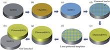
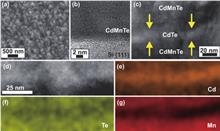
This work shows that despite a lattice mismatch of almost 20%, CdMnTe/CdTe/CdMnTe heterostructures grown directly on Si(111) have surprisingly good optical emission properties. The investigated structures were grown by molecular beam epitaxy and characterized by scanning transmission electron microscopy, macro- and micro-photoluminescence. Low temperature macro-photoluminescence experiments indicate three emission bands which depend on the CdTe layer thickness and have different confinement characteristics. Temperature measurements reveal that the lower energy emission band (at 1.48 eV) is associated to defects and bound exciton states, while the main emission at 1.61 eV has a weak 2D character and the higher energy one at 1.71 eV has a well-defined (zero-dimensional, 0D) 0D nature. Micro-photoluminescence measurements show the existence of sharp and strongly circularly polarized (up to 40%) emission lines which can be related to the presence of Mn in the heterostructure. This result opens the possibility of producing photon sources with the typical spin control of the diluted magnetic semiconductors using the low-cost silicon technology.
Oct. 11, 2024Vol. 45 Issue 9 092301 (2024)
Xiaoyong Jiang, Minrui Ye, Yunhai Li, Xiao Fu, Tangxin Li, Qixiao Zhao, Jinjin Wang, Tao Zhang, Jinshui Miao, and Zengguang Cheng
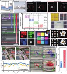
The utilization of processing capabilities within the detector holds significant promise in addressing energy consumption and latency challenges. Especially in the context of dynamic motion recognition tasks, where substantial data transfers are necessitated by the generation of extensive information and the need for frame-by-frame analysis. Herein, we present a novel approach for dynamic motion recognition, leveraging a spatial-temporal in-sensor computing system rooted in multiframe integration by employing photodetector. Our approach introduced a retinomorphic MoS2 photodetector device for motion detection and analysis. The device enables the generation of informative final states, nonlinearly embedding both past and present frames. Subsequent multiply-accumulate (MAC) calculations are efficiently performed as the classifier. When evaluating our devices for target detection and direction classification, we achieved an impressive recognition accuracy of 93.5%. By eliminating the need for frame-by-frame analysis, our system not only achieves high precision but also facilitates energy-efficient in-sensor computing.
Oct. 11, 2024Vol. 45 Issue 9 092401 (2024)
Jieru Song, Jialin Meng, Tianyu Wang, Changjin Wan, Hao Zhu, Qingqing Sun, David Wei Zhang, and Lin Chen
Photoelectric synaptic devices could emulate synaptic behaviors utilizing photoelectric effects and offer promising prospects with their high-speed operation and low crosstalk. In this study, we introduced a novel InGaZnO-based photoelectric memristor. Under both electrical and optical stimulation, the device successfully emulated synaptic characteristics including excitatory postsynaptic current (EPSC), paired-pulse facilitation (PPF), long-term potentiation (LTP), and long-term depression (LTD). Furthermore, we demonstrated the practical application of our synaptic devices through the recognition of handwritten digits. The devices have successfully shown their ability to modulate synaptic weights effectively through light pulse stimulation, resulting in a recognition accuracy of up to 93.4%. The results illustrated the potential of IGZO-based memristors in neuromorphic computing, particularly their ability to simulate synaptic functionalities and contribute to image recognition tasks.
Oct. 11, 2024Vol. 45 Issue 9 092402 (2024)

Yuanzhi Cui, Hongyue Hao, Shihao Zhang, Shuo Wang, Jing Zhang, Yifan Shan, Ruoyu Xie, Xiaoyu Wang, Chuang Wang, Mengchen Liu, Dongwei Jiang, Yingqiang Xu, Guowei Wang, Donghai Wu, Zhichuan Niu, and Derang Cao
This paper examines GaSb short-wavelength infrared detectors employing planar PN junctions. The fabrication was based on the Zn diffusion process and the diffusion temperature was optimized. Characterization revealed a 50% cut-off wavelength of 1.73 μm, a maximum detectivity of 8.73 × 1010 cm·Hz1/2/W, and a minimum dark current density of 1.02 × 10?5 A/cm2. Additionally, a maximum quantum efficiency of 60.3% was achieved. Subsequent optimization of fabrication enabled the realization of a 320 × 256 focal plane array that exhibited satisfactory imaging results. Remarkably, the GaSb planar detectors demonstrated potential in low-cost short wavelength infrared imaging, without requiring material epitaxy or deposition.
Oct. 11, 2024Vol. 45 Issue 9 092403 (2024)
Lu Wang, Xulei Qin, Li Zhang, Kun Xu, Feng Yang, Shaoqian Lu, Yifei Li, Bosen Liu, Guohao Yu, Zhongming Zeng, and Baoshun Zhang
In this work, AlN films were grown using gallium (Ga) as surfactant on 4° off-axis 4H-SiC substrates via microwave plasma chemical vapor deposition (MPCVD). We have found that AlN growth rate can be greatly improved due to the catalytic effect of trimethyl-gallium (TMGa), but AlN crystal structure and composition are not affected. When the proportion of TMGa in gas phase was low, crystal quality of AlN can be improved and three-dimensional growth mode of AlN was enhanced with the increase of Ga source. When the proportion of TMGa in gas phase was high, two-dimensional growth mode of AlN was presented, with the increase of Ga source results in the deterioration of AlN crystal quality. Finally, employing a two-step growth approach, involving the initial growth of Ga-free AlN nucleation layer followed by Ga-assisted AlN growth, high quality of AlN film with flat surface was obtained and the full width at half maximum (FWHM) values of 415 nm AlN (002) and (102) planes were 465 and 597 arcsec.
Oct. 11, 2024Vol. 45 Issue 9 092501 (2024)
Shijie Pan, Shiwei Feng, Xuan Li, Zixuan Feng, Xiaozhuang Lu, Kun Bai, and Yamin Zhang
In this study, the effects of 1 MeV electron radiation on the D-mode GaN-based high electron mobility transistors (HEMTs) were investigated after different radiation doses. The changes in electrical properties of the device were obtained, and the related physical mechanisms were analyzed. It indicated that under the radiation dose of 5 × 1014 cm?2, the channel current cannot be completely pinched off even if the negative gate voltage was lower than the threshold voltage, and the gate leakage current increased significantly. The emission microscopy and scanning electron microscopy were used to determine the damage location. Besides, the radiation dose was adjusted ranging from 5 × 10¹² to 1 × 1014 cm?2, and we noticed that the drain?source current increased and the threshold voltage presented slightly negative shift. By calculations, it suggested that the carrier density and electron mobility gradually increased. It provided a reference for the development of device radiation reinforcement technology.
Oct. 11, 2024Vol. 45 Issue 9 092503 (2024)
© Copyright 2018-2021 | Chinese Laser Press.
All Rights Reserved 沪ICP备15018463号-20